

VIA VT86C100A Datasheet

VIA Technologies, Inc. Preliminary VT86C100A
VT86C100A
PCI FAST ETHERNET CONTROLLER
DATA SHEET
(Preliminary)
DATE : Aug 31, 1997
VIA TECHNOLOGIES, INC.

VIA Technologies, Inc. Preliminary VT86C100A
PRELIMINARY RELEASE
Please contact Via Technologies for the latest documentation.
Copyright Notice:
Copyright © 1995, Via Technologies Incorporated. Printed in Taiwan. ALL RIGHTS RESERVED.
No part of this document may be reproduced, transmitted, transcribed, stored in a retrieval system,
or translated into any language, in any form or by any means, electronic, mechanical, magnetic,
optical, chemical, manual or otherwise without the prior written permission of Via Technologies
Incorporated.
The VT86C100A may only be used to identify products of Via Technologies.
All trademarks are the properties of their respective owners.
Disclaimer Notice:
No license is granted, implied or otherwise, under any patent or patent rights of Via Technologies.
Via Technologies makes no warranties, implied or otherwise, in regard to this document and to the
products described in this document. The information provided by this document is believed to be
accurate and reliable to the publication date of this document. However, Via Technologies
assumes no responsibility for any errors in this document. Furthermore, Via Technologies assumes
no responsibility for the use or misuse of the information in this document and for any patent
infringements that may arise from the use of this document. The information and product
specifications within this document are subject to change at any time, without notice and without
obligation to notify any person of such change.
Offices:
5020 Brandin Court 8th Floor, No. 533
Fremont, CA 94538 Chung-Cheng Rd., Hsin-Tien
USA Taipei, Taiwan ROC
Tel: (510) 683-3300 Tel: (886-2) 218-5452
Fax: (510) 683-3301 Fax: (886-2) 218-5453
Onlines Services:
BBS : 886-2-2186408
FTP : FTP.VIA.COM.TW
HTTP: WWW.VIA.COM.TW

VIA Technologies, Inc. Preliminary VT86C100A
VT86C100A PCI FAST ETHERNET CONTROLLER FEATURES
* Single chip Fast Ethernet controller for PCI bus interface
-- compliant to PCI v2.1 with optional delay transaction and sub-vendor, sub-system- ID
-- Provides a direct connection to PCI bus
-- Supports two network ports : 10/100 M MII interface
* High performance PCI mastering structure
-- VIA self-define 128 bytes memory I/O or register I/O based command and status register
-- Software oriented chain structure description to minimize hardware complexity
-- Include on chip bus master DMA with programmable burst length for low CPU utilization
-- Dynamic transmit packet auto queuing for back auto queuing for bac for back to back transmissin
-- Programmable activity polling intervals for description DMA
-- Programmable DMA arbitration priority to minimize overflow under flow condition
-- Support early receive and early transmit interrupt for software parallel processing
-- Interrupt controllable by receive/transmit descriptor list for saving interrupt service time
* Provides standard 100-M bits MII interface
-- Support 100Base-TX with CAT5 UTP, STP and fiber cables
-- Support 100Base-T4 with CAT3, CAT4, CAT 5 UTP, STP
* 10/100Mhz full duplex, half duplex operation
* Contains two deeper 2K bytes FIFO for receive and transmit controller both supports bursts of
up to full Ethernet length
-- Programmable receive and transmit FIFO threshold control for optimize PCI throughput
* Flexible dynamically load EEPROM algorithm.
-- Load after power-up
-- Dynamic auto reload
-- Embedded programming for configure modification
-- Dynamic direct programming for manufacturing
* Support physical, Broadcast, Multicast address filtering using hashing function
* Support Magic packet and wake on address filtering
* Support external Bootrom up to 64K bytes no external address latch
* Software controllable power down feature
* Single +5V supply, 0.5um standard CMOS technology
* 128 pin PQFP package
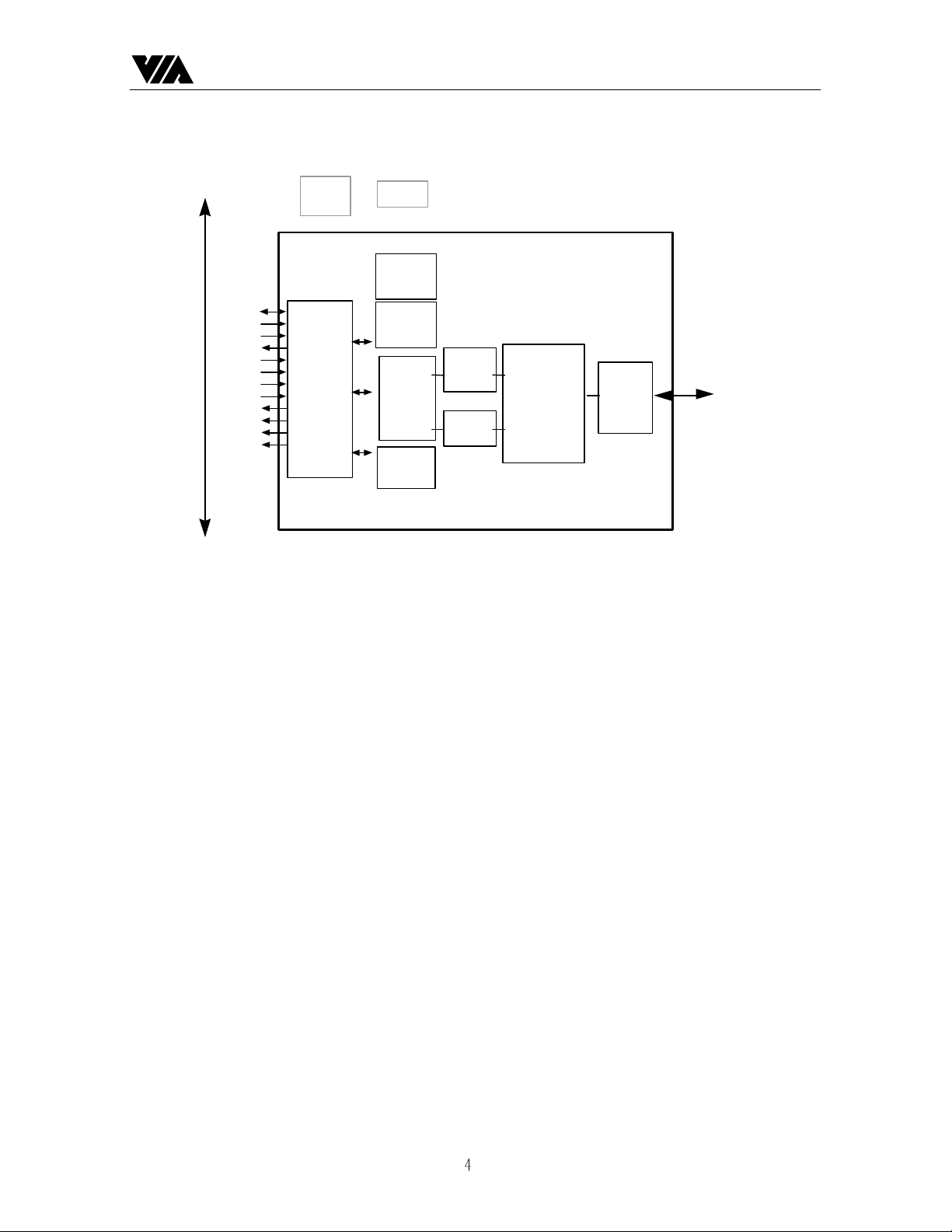
VIA Technologies, Inc. Preliminary VT86C100A
PCI v2.1
AD[31:0]
PCICLK
PCIRST#
INTA#
CBE#[3:0]
IDSEL
FRAME#
IRDY#
TRDY#
DEVSEL#
STOP#
PAR
Boot
ROM
_MSRD,
_MSWR,
EECS
PCI
Bus
Interface
Unit
Config.
EEPROM
Configuration
Registers &
EEPROM Control
Tally Counters
Master
Registers
Machine
Mgmt.
PCI CFG
RxFIFO
2K bytes
&State
&Buffer
TxFIFO
2K bytes
10/100M
MAC Tx/Rx
Protocol
State
Figure 1: Application Diagram
MII
TXD[3:0],
RXD[3:0],
TX_EN
TX_ER, RX_ER
TX_CLK, RX_CLK
RX_DV, CRS, COL
MDIO
VIA Technologies, Inc. Preliminary VT86C100A
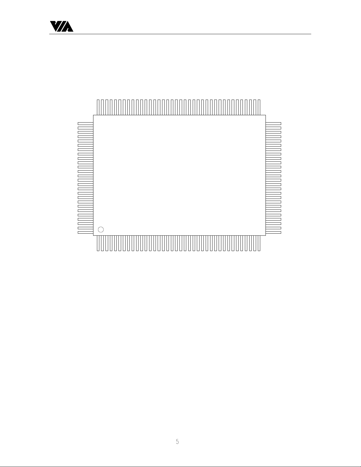
PIN DIAGRAM
MRXC
MRXDV
1
0
2
MTXC
MERR
1
0
0
VSS
VDD
MTXD0
MTXE
9
5
MTXD2
MTXD1
MCOL
MTXD3
TST
MCRS
9
0
VSS
VDD
NC2
MA11
MA12
MA13
MA14
MA15
GPIO1/AUXPME
8
5
8
0
MA9
MA10
VSS
RAMVSS
VDD
7
5
RAMVDD
MA7
MA8
MA6
MA5
7
0
MA4
MA3
MA2
VSS
VDD
6
5
MRXD0
MRXD1
MRXD2
MRXD3
VSS
VDD
MDC
MDIO
HDRST
M10TEN
INTA#
PCIRST#
PCICLK
VSS
VDD
GNT#
REQ#
PME#
AD31
AD30
AD29
AD28
VDD
VSS
AD27
AD26
103
105
110
115
120
125
128
1
AD25
AD24
CEB3#
5
AD23
IDSEL
VSS
AD22
AD21
1
0
VDD
AD20
VT86C100A
1
5
VSS
AD19
AD18
AD17
AD16
CBE2#
FRAME#
IRDY#
TRDY#
2
0
VDD
STOP#
DEVSEL#
VSS
PERR#
2
5
PAR
AD15
CBE1#
AD14
AD13
3
0
AD12
AD11
VSS
AD10
VDD
3
5
AD9
AD8
3
8
AD7
CBE0#
64
MA1
MA0
NC
NC
60
MD7
MD6
MD5
VSS
VDD
55
MD4
MD3
MD2
MD1
MD0
50
BPRD#
ECS
VSS
VDD
AD0
45
AD1
AD2
AD3
AD4
VSS
AD5
39
AD6

VIA Technologies, Inc. Preliminary VT86C100A
PIN DESCRIPTIONS
No. Name Type Description
PCI Bus Interface
121-
124,127-
128,1-
2,5,7-
9,1114,2732,35-
36,38,39-
40,42-46
115
113
114
3,16,26,37
4
17
18
19
20
21
AD31-0 I/O Address/Data are multiplexed on the same PCI pins. A bus transaction
consists of an address phase followed by one or more data phases. The
address phase is the clock cycle in which FRAME# is asserted. Write
data is stable and valid when IRDYB is asserted and read data is stable
and valid when TRDYB is asserted.
PCICLK I PCICLK provides timing for all transactions on PCI and is an input pin
to every PCI device.
INTA# OD INTA# is an asynchronous signal which is used to request an interrupt
PCIRST# I When PCIRST# is asserted low, the VT86C100A chip performs an
internal system hardware reset. PCIRST# may be asynchronous to CLK
when asserted or deasserted. It is recommended that the deassertion be
synchronous to guarantee clean and bounce free edge.
CBE#[3:0] I Bus Command/Byte Enables are multiplexed on the same PCI pins.
During the address phase of a transaction, CBE3-0B define the Bus
Command. Burring the data phase, CBE3-0B are used as Byte Enables.
The Byte Enables define which physical byte lanes carry meaningful
data. CBE0B applies to byte 0 and CBE3B applies to byte 3.
IDSEL I Used as a chip select during PCI configuration cycle.
FRAME# I/O Cycle Frame is driven by the current master to indicate the beginning
and duration of an access. FRAME# is asserted to indicate a bus
transaction is beginning. While FRAME# is asserted, data transfers
continue. When FRAME# is deasserted, the transaction is in the final
data phase.
IRDY# I/O Initiator Ready indicates the initiating agent's ability to complete the
current data phase of the transaction. IRDY# is used in conjunction with
TRDY#. A data phase is completed on any clock when both IRDY# and
TRDY# are asserted. During a write, IRDY# indicates that valid data is
present on AD31-0. During a read, it indicates the master is prepared to
accept data. Wait cycles are inserted until both IRDY# and TRDY# are
asserted simultaneously.
TRDY# I/O Target Ready indicates the target's agent's ability to complete the current
data phase of the transaction. TRDY# is used in conjunction with
IRDY#. A data phase is completed on any clock when both IRDY# and
TRDY# are asserted. During a read, TRDY# indicates that valid data is
present on AD31-0. During a write, it indicates the target is prepared to
accept data. Wait cycles are inserted until both IRDY# and TRDY# are
asserted simultaneously.
DEVSEL# I/O Device Select, when actively driven, indicates the driving device has
decoded its address as the target of the current access. As an input,
DEVSEL# indicates whether any device on the bus has been selected.
STOP# I/O VT86C100A drives STOP# to disconnect further traction.
VIA Technologies, Inc. Preliminary VT86C100A
25
PAR T/S Parity is even parity across AD31-0 and CBE3-0B. PAR is stable and
valid one clock after the address phase. For data phases PAR is stable
and valid one clock after either IRDY# is asserted on a write transaction
or TRDY# is asserted on a read transaction.
118
GNT# I Bus grant asserts to indicate to the VT86C100A that access to the bus is
granted.
119
REQ# O Bus request is asserted by the bus master indicate to the bus arbiter that
it wants to use the bus.
23
120
111
PERR# I/O Parity error asserts when a data parity error is detected
PME# O Power management event interrupt
HDRST O When PCIRST# is asserted low, the VT86C100A chip performs an
internal system hardware reset. Then HDRST is asserted high for
external device reset signal like PHY device.
Network Interface
91 MCOL I Collision detect when the external PHY device
90 MCRS I Carrier sense is asserted by the external PHY when the media is active
92-95 MTXD[3-0] O MII 4 parallel transmit data lines. This data be synchronized to assertion
by the MTXC signal
96 MTXEN O Transmit enable signals that the transmit is active in the MII port to an
external PHY device
99 MTXC I MII transmit clock supports the 25mhz or 2.5mhz transmit clock
supplied by the external PMD device. This clock should always be
active.
100 MERR I MII receive error asserts when a data decoding error is detected by
external PHY device.
101 MRXC I MII receive clock supports the 25mhz or 2.5mhz clock. This clock is
recovered by the PHY.
102 MRXDV I MII data valid
103-106 MRXD[0-3] I Four parallel receive data lines. This data be driven from external PHY
be synchronized with MRXC signal.
109 MDC O MII management data clock be soured by VT86C100A MDC bit
(MIIR:0) to the external PHY devices as timing reference for the
MDIO signal.
110 MDIO I/O MII management data input/output, read from MDI bit (MIIR:1) or
written from MDO bit (MIIR:2)
112 GPIO I/O GPIO
External Memory Support & General purpose I/O support
49 EECS O EEPROM Chip Select: Chip select signal for the external EEPROM
when a EEPROM is used to provide the configuration data and
Ethernet Address. A 100K pull-up resistor is connected.
50 BPRD# O Boot PROM Read: Read the Boot ROM on the memory support data
bus.
51 MD0/
EEDO
52 MD1/
EEDI
I/O Bootrom data 0
Serial ROM Data output
O/O Bootrom data 1
Serial ROM Data input
53 MD2/ EECLK O/O Bootrom data 2
Serial ROM Clock signal
54-55,58-
MD3-7 I/O Bootrom Data [3-7] :
60

VIA Technologies, Inc. Preliminary VT86C100A
63-64,67-
MA0-MA15 O Bootrom address line [0-15]
73,78-
84
85 GPIO1/AUXP
IO General purpose input and output 1 : usually as Magic key interrupt line
ME
112 GPIO2/LKC IO General purpose input and output 2, this pin usually as link change status
from external PHY device.
Power Supply & Ground
10,22,34,47,
56,65,76,
87,97,108
,117,125
6,15,24,33,
41,48,57
,66,75,7
7,88,98,
107,116,
126
VDD, VDDA P Positive 5V Supply: Supply power to Internal digital logic, Digital I/O
pads, and TD, TX pads. Double bonding may be required.
VSS, VSSA G Negative Supply: digital ground. Multiple bonding pads are
required to separate core and I/O pads ground.

VIA Technologies, Inc. Preliminary VT86C100A
FUNCTIONAL DESCRIPTIONS
1. GENERAL DESCRIPTION
The VT86C100A Rhine ACPI PCI bus master 100 M FAST Ethernet controller is CMOS VLSI designed for
easy implementation of CSMA/CD IEEE 802.3u 100M local area networks. Significant features include:
twisted-pair interface, PCI Plug&Play compatibility, 32 bit bus mastering, powerful buffer management and
Early Interrupt Receive/Transmit.
The VT86C100A integrates the entire bus interface of PCI systems. Setting hardware jumpers or software
configures the VT86C100A bus interface. The VT86C100A also complies with PCI specification v2.1.. The
VT86C100A supports the Media Independent Interface (MII) network interface.
1.1 FIFO AND CONTROL LOGIC
The VT86C100A incorporates two independent 2K bytes deeper FIFO for transmit or receive data from
system interface or to the network interface, providing temporary storage of data, free host system from the
real-time demands on network.
The VT86C100A enhanced the FIFO management logic to handle received data packets up to four packets
before transfer to system data buffer. This ability reduce the packets losing due to PCI bus mastering abrition
latency.
2. NETWORK INTERFACE
The VT86C100A Rhine ACPI support one MII interface
2.1 MII Interface
The MII interface is an IEEE 802.3 compliant interface that provides a simple and easy interconnection
between the MAC layer and PHY device. This interface has support the following characteristics :
• Support both 10M and 100M data rate.
• Contains data and synchronous clock
• 4-bit independent receive and transmit data.
• Uses TTL signal levels and compatibles with common CMOS processes.
VIA Technologies, Inc. Preliminary VT86C100A
3. EEPROM Interface and Programming
VT86C100A uses an 93C46 to store configuration data and Ethernet address.
3.1. EEPROM Contents
D15 D0
3FH
.
.
.
.
.
.
10H
0FH 73H 73H
0EH CFG_D CFG_C
0DH CFG_B CFG_A
0CH BCR1 BCR0
0BH MAX_LAT MIN_GNT
0AH Reserved Reserved
09H KEY5 KEY5
08H KEY3 KEY2
07H KEY1 KEY0
06H Reserved Reserved
05H SUBVID1 SUBVID0
04H SUBSID1 SUBSID0
03H Reserved Reserved
02H Ethernet Address 5 Ethernet Address 4
01H Ethernet Address 3 Ethernet Address 2
00H Ethernet Address 1 Ethernet Address 0
Note 1. The word on location 03H is optional to user's application requirement.
Note 2. Programming 73H into the upper address is required to protect the Ethernet address from being destroyed accidentally
Note 3. The word on location 04H, 05H is sub-System ID, sub-Vendor ID in PCI specification 2.1.
Reserved for 93C46
.
.
.
.
.
.
.
Reserved for 93C46
.
.
.
.
.
.
.
3.2. DIRECT PROGRAMMING OF EEPROM
The VT86C100A features a easy way to program external EEPROM in-situ. When the RESET is active and if
the upper byte of 0FH on EEPROM is not 73H, the EEPR bit will not be set to indicate that the current
EEPROM has not been programmed yet. This will allow the VT86C100A to enter Direct Programming mode
if EELOAD is also set. In this mode the user can directly control the EEPROM interface signals by writing to
the ECSR Port and the value on the EECS, ESK and EDI bits will be driven onto the EECS, SK(MD2), and
DI(MD1) outputs respectively. These outputs will be latched so the user can generate a clock on SK by
repetitively writing 1 then 0 to the appropriate bit. This can be used to generate the EEPROM signals as per
the 93C46 data sheet.
To read the EEPROM data, users have to generate EEPROM interface signals into EECS, DI and SK as
described above and in the mean time read the data from DO(MD0) input via pin SD0. Reading Data
Transfer Port during programming will not affect the latched data on EECS, SK, and DI outputs. When the
 Loading...