

Page 1

Data Sheet
VT8235M
Version CD
South Bridge
Revision 2.03
March 16, 2005
VIA TECHNOLOGIES, INC.
Page 2

Copyright Notice:
Copyright © 2002-2005 VIA Technologies Incorporated. All Rights Reserved. No part of this document may be reproduced, transmitted,
transcribed, stored in a retrieval system or translated into any language, in any form or by any means, electronic, mechanical, magnetic, optical,
chemical, manual or otherwise without the prior written permission of VIA Technologies Incorporated. The material in this document is for
information only and is subject to change without notice. VIA Technologies Incorporated reserves the right to make changes in the product design
without reservation and without notice to its users.
Trademark Notices:
VT8235M may only be used to identify products of VIA Technologies.
is a registered trademark of VIA Technologies.
AMD-K7™ and Athlon™ are registered trademarks of Advanced Micro Devices.
Celeron™, Pentium™, Pentium II™, Pentium III™, Pentium 4™, MMX™ and Intel™ are registered trademarks of Intel Corporation.
Windows XP™, Windows 2000™, Windows ME™, Windows 98™ and Plug and Play™ are registered trademarks of Microsoft Corporation.
PCI™ is a registered trademark of the PCI Special Interest Group.
PS/2™ is a registered trademark of International Business Machines Corporation.
All trademarks are the properties of their respective owners.
Disclaimer Notice:
No license is granted, implied or otherwise, under any patent or patent rights of VIA Technologies. VIA Technologies makes no warranties, implied
or otherwise, in regard to this document and to the products described in this document. The information provided by this document is believed to
be accurate and reliable as of the publication date of this document. However, VIA Technologies assumes no responsibility for any errors in this
document. Furthermore, VIA Technologies assumes no responsibility for the use or misuse of the information in this document and for any patent
infringements that may arise from the use of this document. The information and product specifications within this document are subject to change
at any time, without notice and without obligation to notify any person of such change.
Offices:
USA Office: Taipei Office:
940 Mission Court 1
Fremont, CA 94539 Chung-Cheng Road, Hsin-Tien
USA Taipei, Taiwan ROC
Tel: (510) 683-3300 Tel: (886-2) 2218-5452
Fax: (510) 683-3301 or (510) 687-4654 Fax: (886-2) 2218-5453
Web: http://www.viatech.com
Web: http://www.via.com.tw
st
Floor, No. 531
Page 3

VT8235M Version CD V-Link South Bridge
REVISION HISTORY
Document Release Date Revision Initials
1.21 9/27/02 Fixed pin names of PCREQA/B and PCGNTA/B in pin descriptions DH
1.22 10/24/02 Fixed register references in MSCK and MSDT pin descriptions
Fixed VLVREF voltage for V-Link 8x mode
Removed references to nonexistent ports 72-73
1.3 11/20/02 Updated LAN I/O Rx23-20[10], 27-24[15-11], 6F[2-0], 70[6-0], 74[4-0], 83, 84, 86 DH
1.31 12/11/02 Fixed IORDY signal name polarity in pin diagram; fixed minor typos in pin lists
Added strap description in VAD7 pin description; Fixed Func 0 Rx7C[3-0], 98[7,3]
Fixed VIA logo in page heading starting on page 6
1.4 12/17/02 Fixed first two feature bullets to indicate current north bridge products
Improved DPSLP# pin description; Fixed GPO22-23, 28-29 pin descriptions
Fixed note in VCC pin description; Improved bit description for D17 F0 RxE5[3]
1.41 1/3/03 Updated Port 61 (bits 7-6 and 3-2) and Port 92 (bits 7-6 and 3)
Device 16 Function 0-3 USB – added Rx83-80; renamed F3 Rx48-49
Device 17 Function 1 IDE – fixed Rx4E register name; removed RxFD
Fixed Rx3C[3-0] of Device 17 Function 1, 5, 6 and Device 18 Function 0
Fixed Rx2C-2F of Device 17 Function 5-6 and RxB of Function 6
1.42 1/3/03 Fixed Device Ids in table 5 function summary for USB 2.0 and LAN DH
1.43 2/5/03 Changed Device 17 Function 0 Rx50[0] to reserved DH
1.44 2/5/03 Updated feature bullets to indicated compatibility with ACPI 2.0 DH
1.5 2/25/03 Updated figure 1 block diagram; Updated defaults in GPI pin description table
Added strap on SDCS1# in ballout & pin lists and added to strap pin description table
Updated Device 16 Function 0-3 Rx83 default; Removed PMIO Rx5C[1]
Device 17 Function 0 – fixed Rx50[1] bit name, 95[2] bit description
1.51 3/3/03 Fixed EEDI and EEDO pin directions; added register cross references to GPIOC-E DH
1.52 3/18/03 Updated GPI/GPO pin default states
Fixed PMIO Rx30[1] cross-reference to Device 17 Function 0 Rx84
1.6 4/15/03 Fixed IDE Rx3D default, fixed D17 F0 Rx8C[7-4],8D[4]; updated PMIO Rx10[3-0]
Fixed incorrect JEDEC-spec reference in mechanical specification diagram
1.7 4/29/03 Added “Version CD” to product name to differentiate from “Version CE”
Fixed VT8233A Version CE / VT8235ML South Bridge part # references
1.71 6/9/03 Updated Dev 17 Func 0 Rx59[3-2], PMIO RxB-8[31-24], Dev 17 Func 1 Rx4C DH
1.72 6/30/03 Changed pins W22 and AD17 to NC DH
1.73 9/17/03 Removed power requirements table; Updated PMIO Rx5-4[12:10] AL
1.74 3/3/04 Moved straps to separate table; Updated IO Trap registers Rx5C[0]
Updated Dev18 Func 0 Rx06[7:5], 07[7:3], 08[0], 09[0], 0C[4], 0D[1:0], 23-20[7], 4340[11], 6E[5:3], 6F[5:3]
1.75 4/20/04 Updated top marking on Mechanical Specification section; Fixed Pin AD7, AE7 IO
Prosperity
1.76 5/10/04 Updated Device18 Function 0 Rx7B VL
1.77 7/9/04 Added lead-free package diagram to mechanical specification section VL
1.78 8/11/04 Updated lead-free diagram in mechanical specification VL
1.79 8/26/04 Updated APIC Fixed IRQ Routing Table in register descriptions
Fixed incorrect reference in Device17 Function 0 Rx81
2.0 9/3/04 Changed part to VT8235M Version CD VL
2.01 11/4/04 Updated Rx48 and Rx49 in Device 17 Function 5 and 6
Updated bit definition for D17F0 Rx80[5]; Added D17F0 RxEC-EF
2.02 11/23/04 Updated top marking on mechanical specification VL
2.03 3/16/05 Added USBREXT signal description and updated copyright notice DA
DH
DH
DH
DH
DH
DH
DH
DH
VL
VL
VL
JE
Revision 2.03, March 16, 2005 -iii- Revision History
Page 4

VT8235M Version CD V-Link South Bridge
TABLE OF CONTENTS
REVISION HISTORY ....................................................................................................................................................................III
TABLE OF CONTENTS.................................................................................................................................................................IV
LIST OF FIGURES ....................................................................................................................................................................... VII
LIST OF TABLES ......................................................................................................................................................................... VII
PRODUCT FEATURES.................................................................................................................................................................... 1
OVERVIEW....................................................................................................................................................................................... 4
PINOUTS............................................................................................................................................................................................ 6
PIN DESCRIPTIONS........................................................................................................................................................................ 9
V-LINK PIN DESCRIPTIONS ........................................................................................................................................................... 9
CPU, APIC AND CPU CONTROL PIN DESCRIPTIONS ............................................................................................................... 10
MII, SERIAL EEPROM, LPC AND DMA PIN DESCRIPTIONS .................................................................................................. 12
USB, SMB AND PROGRAMMABLE CHIP SELECT PIN DESCRIPTIONS ....................................................................................... 13
EIDE INTERFACE PIN DESCRIPTIONS ........................................................................................................................................ 14
SERIAL IRQ AND AC97 PIN DESCRIPTIONS............................................................................................................................... 15
INTERNAL KEYBOARD CONTROLLER AND SPEAKER PIN DESCRIPTIONS ................................................................................. 16
GENERAL PURPOSE INPUT PIN DESCRIPTIONS .......................................................................................................................... 17
GENERAL PURPOSE OUTPUT AND GPIO PIN DESCRIPTIONS .................................................................................................... 18
POWER MANAGEMENT AND EVENT DETECTION PIN DESCRIPTIONS ....................................................................................... 19
CLOCK, RESETS, POWER STATUS, POWER AND GROUND PIN DESCRIPTIONS ......................................................................... 20
STRAP PIN DESCRIPTIONS ........................................................................................................................................................... 21
REGISTERS..................................................................................................................................................................................... 22
REGISTER OVERVIEW ................................................................................................................................................................. 22
REGISTER DESCRIPTIONS ........................................................................................................................................................... 37
Legacy I/O Ports................................................................................................................................................................... 37
Keyboard Controller I/O Registers........................................................................................................................................................ 38
DMA Controller I/O Registers .............................................................................................................................................................. 40
Interrupt Controller I/O Registers.......................................................................................................................................................... 41
Timer / Counter Registers......................................................................................................................................................................41
CMOS / RTC I/O Registers................................................................................................................................................................... 42
Keyboard / Mouse Wakeup Index / Data Registers........................................................................................................... 43
Keyboard / Mouse Wakeup Registers................................................................................................................................. 43
Memory Mapped I/O APIC Registers ................................................................................................................................ 44
Indexed I/O APIC Registers ................................................................................................................................................ 44
Configuration Space I/O ...................................................................................................................................................... 46
Device 16 Function 0 Registers - USB 1.1 UHCI Ports 0-1 ............................................................................................... 47
PCI Configuration Space Header...........................................................................................................................................................47
USB-Specific Configuration Registers.................................................................................................................................................. 48
USB I/O Registers................................................................................................................................................................................. 50
Device 16 Function 1 Registers - USB 1.1 UHCI Ports 2-3 ............................................................................................... 51
PCI Configuration Space Header...........................................................................................................................................................51
USB-Specific Configuration Registers.................................................................................................................................................. 52
Revision 2.03, March 16, 2005 -iv- Table of Content
Page 5

VT8235M Version CD V-Link South Bridge
USB I/O Registers................................................................................................................................................................................. 54
Device 16 Function 2 Registers - USB 1.1 UHCI Ports 4-5 ............................................................................................... 55
PCI Configuration Space Header...........................................................................................................................................................55
USB-Specific Configuration Registers.................................................................................................................................................. 56
USB I/O Registers................................................................................................................................................................................. 58
Device 16 Function 3 Registers - USB 2.0 EHCI................................................................................................................ 59
PCI Configuration Space Header...........................................................................................................................................................59
USB-Specific Configuration Registers.................................................................................................................................................. 60
EHCI USB 2.0 I/O Registers................................................................................................................................................................. 61
Device 17 Function 0 Registers – Bus Control and Power Management......................................................................... 62
PCI Configuration Space Header...........................................................................................................................................................62
ISA Bus Control .................................................................................................................................................................................... 63
Miscellaneous Control........................................................................................................................................................................... 65
Function Control.................................................................................................................................................................................... 66
Serial IRQ, LPC, and PC/PCI DMA Control ........................................................................................................................................ 67
Plug and Play Control - PCI .................................................................................................................................................................. 67
GPIO and Miscellaneous Control.......................................................................................................................................................... 68
Programmable Chip Select Control....................................................................................................................................................... 70
ISA Decoding Control........................................................................................................................................................................... 71
Power Management-Specific Configuration Registers.......................................................................................................................... 73
System Management Bus-Specific Configuration Registers ................................................................................................................. 80
SMB GPIO Slave Command Codes...................................................................................................................................................... 80
General Purpose I/O Control Registers ................................................................................................................................................. 81
Watchdog Timer Registers .................................................................................................................................................................... 82
Power Management I/O-Space Registers .............................................................................................................................................. 83
System Management Bus I/O-Space Registers...................................................................................................................................... 92
Device 17 Function 1 Registers - Enhanced IDE Controller............................................................................................. 95
PCI Configuration Space Header...........................................................................................................................................................95
IDE-Controller-Specific Configuration Registers ................................................................................................................................. 97
IDE Power Management Registers...................................................................................................................................................... 101
IDE Back Door Registers .................................................................................................................................................................... 101
IDE I/O Registers................................................................................................................................................................................ 101
Device 17 Function 5 Registers - AC97 Audio Controller............................................................................................... 102
PCI Configuration Space Header.........................................................................................................................................................102
Audio-Specific PCI Configuration Registers....................................................................................................................................... 103
I/O Base 0 Regs – Audio Scatter / Gather DMA ................................................................................................................................. 105
Device 17 Function 6 Registers - AC97 Modem Controller............................................................................................ 114
PCI Configuration Space Header.........................................................................................................................................................114
Modem-Specific PCI Configuration Registers.................................................................................................................................... 115
I/O Base 0 Regs – Modem Scatter / Gather DMA............................................................................................................................... 117
Device 18 Function 0 Registers - LAN .............................................................................................................................. 120
PCI Configuration Space Header.........................................................................................................................................................120
LAN-Specific PCI Configuration Registers ........................................................................................................................................ 120
LAN I/O Registers............................................................................................................................................................................... 122
FUNCTIONAL DESCRIPTIONS................................................................................................................................................ 133
POWER MANAGEMENT.............................................................................................................................................................. 133
Power Management Subsystem Overview .......................................................................................................................................... 133
Processor Bus States............................................................................................................................................................................ 133
System Suspend States and Power Plane Control................................................................................................................................ 134
General Purpose I/O Ports................................................................................................................................................................... 134
Power Management Events ................................................................................................................................................................. 135
System and Processor Resume Events................................................................................................................................................. 135
Legacy Power Management Timers .................................................................................................................................................... 136
System Primary and Secondary Events ............................................................................................................................................... 136
Peripheral Events................................................................................................................................................................................. 136
ELECTRICAL SPECIFICATIONS ............................................................................................................................................ 137
ABSOLUTE MAXIMUM RATINGS ............................................................................................................................................... 137
DC CHARACTERISTICS.............................................................................................................................................................. 137
REGISTER BITS POWERED BY VBAT ....................................................................................................................................... 138
Revision 2.03, March 16, 2005 -v- Table of Content
Page 6

VT8235M Version CD V-Link South Bridge
REGISTER BITS POWERED BY VSUS25 .................................................................................................................................... 138
PACKAGE MECHANICAL SPECIFICATIONS...................................................................................................................... 139
Revision 2.03, March 16, 2005 -vi- Table of Content
Page 7

VT8235M Version CD V-Link South Bridge
LIST OF FIGURES
FIGURE 1. PC SYSTEM CONFIGURATION USING THE VT8235M VERSION CD........................................................... 5
FIGURE 2. BALL DIAGRAM (TOP VIEW)................................................................................................................................. 6
FIGURE 3. POWER MANAGEMENT SUBSYSTEM BLOCK DIAGRAM......................................................................... 133
FIGURE 4. SYSTEM BLOCK DIAGRAM USING THE P4X400 NORTH BRIDGE .......................................................... 135
FIGURE 5. MECHANICAL SPECIFICATIONS – 487 PIN BALL GRID ARRAY PACKAGE ........................................ 139
FIGURE 6. LEAD-FREE MECHANICAL SPECIFICATIONS – 487 PIN BALL GRID ARRAY PACKAGE ................ 140
LIST OF TABLES
TABLE 1. PIN LIST (NUMERICAL ORDER) ............................................................................................................................. 7
TABLE 2. PIN LIST (ALPHABETICAL ORDER) ...................................................................................................................... 8
TABLE 3. MEMORY MAPPED REGISTERS ........................................................................................................................... 22
TABLE 4. FUNCTION SUMMARY............................................................................................................................................. 22
TABLE 5. SYSTEM I/O MAP....................................................................................................................................................... 22
TABLE 6. REGISTERS ................................................................................................................................................................. 23
TABLE 7. KEYBOARD CONTROLLER COMMAND CODES .............................................................................................. 39
TABLE 8. CMOS REGISTER SUMMARY ................................................................................................................................ 42
TABLE 9. APIC FIXED IRQ ROUTING .................................................................................................................................... 65
TABLE 10. PNP IRQ ROUTING TABLE ................................................................................................................................... 67
Revision 2.03, March 16, 2005 -vii- Table of Content
Page 8

VT8235M Version CD V-Link South Bridge
VT8235M VERSION CD
LOW COST V-LINK CLIENT
IGHLY INTEGRATED SOUTH BRIDGE
H
HIGH BANDWIDTH V-LINK CLIENT CONTROLLER
NTEGRATED FAST ETHERNET,
I
I
NTEGRATED DIRECT SOUND AC97 AUDIO,
LTRADMA-133/100/66/33 MASTER MODE EIDE CONTROLLER,
U
S
IX PORT USB 2.0 CONTROLLER, KEYBOARD / MOUSE CONTROLLER,
RTC, LPC, SMB
US, SERIAL IRQ, PLUG AND PLAY, ACPI,
AND PC2001 COMPLIANT ENHANCED POWER MANAGEMENT
PRODUCT FEATURES
• Inter-operable with VIA Host-to-V-Link Host Controller
− Combine with KT400A North Bridge for a complete Athlon system
− Combine with CLE266 North Bridge for a complete VIA C3 / Pentium 3 system
− Combine with P4X400 North Bridge for a complete Pentium 4 system
• High Bandwidth 533 MB/s 8-bit V-Link Client Controller
− Supports 66 MHz V-Link Client interface with total bandwidth of 533 MB/sec
− V-Link operates in 2x, 4x, and 8x modes
− Full duplex commands with separate Strobe / Command
− Request / Data split transaction
− Configurable outstanding transaction queue for V-Link Client accesses
− Auto Client Retry to eliminate V-Link Host-Client Retry cycles
− Intelligent V-Link transaction protocol to eliminate data wait-state / throttle transfer latency; all V-Link transactions
for both Host and Client have a consistent view of transaction data depth and buffer size to avoid data overflow.
− Highly efficient V-Link arbitration with minimum overhead; all V-Link transactions have predictable cycle length
with known Command / Data duration
− Auto connect / reconnect capability and dynamic stop for minimum power consumption
− Parity checking to insure correct data transfers
• Integrated Peripheral Controllers
−
Integrated Fast Ethernet Controller with 1 / 10 / 100 Mbit capability
− Integrated USB 2.0 Controller with three root hubs and six function ports
− Dual channel UltraDMA-133 / 100 / 66 / 33 master mode EIDE controller
− AC-link interface for AC-97 audio codec and modem codec
− HSP modem support
− Integrated DirectSound compatible digital audio controller
− LPC interface for Low Pin Count interface to Super-I/O or ROM
• Integrated Legacy Functions
− Integrated Keyboard Controller with PS2 mouse support
− Integrated DS12885-style Real Time Clock with extended 256 byte CMOS RAM and Day/Month Alarm for ACPI
− Integrated DMA, timer, and interrupt controller
− Serial IRQ for docking and non-docking applications
− Fast reset and Gate A20 operation
Revision 2.03, March 16, 2005 -1- Product Feature
Page 9

VT8235M Version CD V-Link South Bridge
• Concurrent PCI Bus Controller
− 33 MHz operation
− Supports up to six PCI masters
− Peer concurrency
− Concurrent multiple PCI master transactions; i.e., allow PCI masters from both PCI buses active at the same time
− Zero wait state PCI master and slave burst transfer rate
− PCI to system memory data streaming up to 132Mbyte/sec (data sent to north bridge via high speed V-Link
Interface)
− PCI master snoop ahead and snoop filtering
− Eight DW of CPU to PCI posted write buffers
− Byte merging in the write buffers to reduce the number of PCI cycles and to create further PCI bursting possibilities
− Enhanced PCI command optimization (MRL, MRM, MWI, etc.)
− Four lines of post write buffers from PCI masters to DRAM
− Sixteen levels (double-words) of prefetch buffers from DRAM for access by PCI masters
− Delay transaction from PCI master accessing DRAM
− Transaction timer for fair arbitration between PCI masters (granularity of two PCI clocks)
− Symmetric arbitration between Host/PCI bus for optimized system performance
− Complete steerable PCI interrupts
− PCI-2.2 compliant, 32 bit 3.3V PCI interface with 5V tolerant inputs
• Fast Ethernet Controller
− High performance PCI master interface with scatter / gather and bursting capability
− Standard MII interface to external PHYceiver
− 1 / 10 / 100 MHz full and half duplex operation
− Independent 2K byte FIFOs for receive and transmit
− Flexible dynamically loadable EEPROM algorithm
− Physical, Broadcast, and Multicast address filtering using hashing function
− Magic packet and wake-on-address filtering
− Software controllable power down
• UltraDMA-133 / 100 / 66 / 33 Master Mode EIDE Controller
− Dual channel master mode hard disk controller supporting four Enhanced IDE devices
− Transfer rate up to 133MB/sec to cover PIO mode 4, multi-word DMA mode 2 drives, and UltraDMA-133 interface
− Increased reliability using UltraDMA-133/100/66 transfer protocols
− Thirty-two levels (doublewords) of prefetch and write buffers
− Dual DMA engine for concurrent dual channel operation
− Bus master programming interface for SFF-8038i rev.1.0 and Windows-95 compliant
− Full scatter gather capability
− Support ATAPI compliant devices including DVD devices
− Support PCI native and ATA compatibility modes
− Complete software driver support
• Direct Sound Ready AC97 Digital Audio Controller
− AC-Link access to 4 CODECs (AC97 + AMC97 + MC97)
− Multichannel Audio
− Bus Master Scatter / Gather DMA
− Dedicated read and write channels supporting simultaneous stereo playback and record
− Dedicated read and write channels supporting simultaneous modem receive and transmit
− 1 stereo DirectSound channel with source / volume control / mixer
− 1 shared FM / SPDIF PCM read channel
− 1 dedicated channel supporting multi-channel audio
− 32-byte line-bufers for each SGD channel
− Programmable 8bit / 16bit mono / stereo PCM data format support
− AC97 2.1 compliant
Revision 2.03, March 16, 2005 -2- Product Feature
Page 10

VT8235M Version CD V-Link South Bridge
• System Management Bus Interface
− Host interface for processor communications
− Slave interface for external SMBus masters
• Universal Serial Bus Controller
USB v2.0 and Enhanced Host Controller Interface (EHCI) v1.0 compatible
−
− USB v1.1 and Universal Host Controller Interface (UHCI) v1.1 compatible
− Eighteen level (doublewords) data FIFO with full scatter and gather capability
− Three root hubs and six function ports
− Integrated physical layer transceivers with optional over-current detection status on USB inputs
− Legacy keyboard and PS/2 mouse support
• Sophisticated PC2001-Compatible Mobile Power Management
− Supports both ACPI (Advanced Configuration and Power Interface) and legacy (APM) power management
− ACPI v2.0 Compliant
− APM v1.2 Compliant
− CPU clock throttling and clock stop control for complete ACPI C0 to C3 state support
− PCI bus clock run, Power Management Enable (PME) control, and PCI/CPU clock generator stop control
− Supports multiple system suspend types: power-on suspends with flexible CPU/PCI bus reset options,
suspend to DRAM, and suspend to disk (soft-off), all with hardware automatic wake-up
− Multiple suspend power plane controls and suspend status indicators
− One idle timer, one peripheral timer and one general purpose timer, plus 24/32-bit ACPI compliant timer
− Normal, doze, sleep, suspend and conserve modes
− Global and local device power control
− System event monitoring with two event classes
− Primary and secondary interrupt differentiation for individual channels
− Dedicated input pins for power and sleep buttons, external modem ring indicator, and notebook lid open/close for
system wake-up
− 32 general purpose input ports and 32 output ports
− Multiple internal and external SMI sources for flexible power management models
− Enhanced integrated real time clock (RTC) with date alarm, month alarm, and century field
− Thermal alarm on external temperature sensing circuit
− I/O pad leakage control
• Plug and Play Controller
− PCI interrupts steerable to any interrupt channel
− Steerable interrupts for integrated peripheral controllers: USB, floppy, serial, parallel, and audio
− Microsoft Windows XP
TM
, Windows NTTM, Windows 2000TM, Windows 98
TM
and plug and play BIOS compliant
• Built-in NAND-tree pin scan test capability
• 0.22um, 2.5V, low power CMOS process
• Single chip 27 x 27 mm, 1.0 mm ball pitch, 487 pin BGA
Revision 2.03, March 16, 2005 -3- Product Feature
Page 11

VT8235M Version CD V-Link South Bridge
OVERVIEW
The VT8235M Version CD South Bridge is a high integration, high performance, power-efficient, and high compatibility device
that supports Intel and non-Intel based processor to V-Link bus bridge functionality to make a complete Microsoft PC2001compliant PCI/LPC system. The VT8235M Version CD includes standard intelligent peripheral controllers:
a) IEEE 802.3 compliant 10 / 100 Mbps PCI bus master Ethernet MAC with standard MII interface to external PHYceiver.
b) Master mode enhanced IDE controller with dual channel DMA engine and interlaced dual channel commands. Dedicated
FIFO coupled with scatter and gather master mode operation allows high performance transfers between PCI and IDE
devices. In addition to standard PIO and DMA mode operation, the VT8235M Version CD also supports the UltraDMA133, 100, 66, and 33 standards to allow reliable data transfer at rates up to 133 MB/sec. The IDE controller is SFF-8038i
v1.0 and Microsoft Windows-family compliant.
c) Universal Serial Bus controller that is USB v2.0 / 1.1 and Universal HCI v2.0 / 1.1 compliant. The VT8235M Version CD
includes three root hubs with six function ports with integrated physical layer transceivers. The USB controller allows hot
plug and play and isochronous peripherals to be inserted into the system with universal driver support. The controller also
implements legacy keyboard and mouse support so that legacy software can run transparently in a non-USB-aware operating
system environment.
d) Keyboard controller with PS2 mouse support.
e) Real Time Clock with 256 byte extended CMOS. In addition to the standard ISA RTC functionality, the integrated RTC also
includes the date alarm, century field, and other enhancements for compatibility with the ACPI standard.
f) Notebook-class power management functionality compliant with ACPI and legacy APM requirements. Multiple sleep states
(power-on suspend, suspend-to-DRAM, and suspend-to-Disk) are supported with hardware automatic wake-up. Additional
functionality includes event monitoring, CPU clock throttling and stop (Intel processor protocol), PCI bus clock stop control,
modular power, clock and leakage control, hardware-based and software-based event handling, general purpose I/O, chip
select and external SMI.
g) Full System Management Bus (SMBus) interface.
h) Integrated bus-mastering dual full-duplex direct-sound AC97-link-compatible sound system.
i) Plug and Play controller that allows complete steerability of all PCI interrupts and internal interrupts / DMA channels to any
interrupt channel. One additional steerable interrupt channel is provided to allow plug and play and reconfigurability of onboard peripherals for Windows family compliance.
The VT8235M Version CD also enhances the functionality of the standard ISA peripherals. The integrated interrupt controller
supports both edge and level triggered interrupts channel by channel. The integrated DMA controller supports type F DMA in
addition to standard ISA DMA modes. Compliant with the PCI-2.2 specification, the VT8235M Version CD supports delayed
transactions and remote power management so that slower ISA peripherals do not block the traffic of the PCI bus. Special
circuitry is built in to allow concurrent operation without causing dead lock even in a PCI-to-PCI bridge environment. The chip
also includes eight levels (doublewords) of line buffers from the PCI bus to the ISA bus to further enhance overall system
performance.
Revision 2.03, March 16, 2005 -4- Overview
Page 12

VT8235M Version CD V-Link South Bridge
p
CPU / Cac h e
CA
North Bridge
CD
M A / Co mma n d
MD
Sys tem Memory
Sideband Signals
Init / A20M#
INTR / NMI
SMI / StopClk
Vl i n k
Interface
SMB
DIMM Module ID
Expansion
Ca rd s
FERR / IGNNE
Slee
Boo t ROM
LPC
VT8235M
487 BGA
IDE Primary and Secondary
PCI
USB 2.0 Ports 0-5
Onboard
LPC I/ O
Keyboard / Mouse
AC97 Link
APIC
RTC
Cry s t a l
Figure 1. PC System Configuration Using the VT8235M Version CD
GPIO, Power Control, Reset
MII Fast Ethernet Interface
Revision 2.03, March 16, 2005 -5- Overview
Page 13
VT8235M Version CD V-Link South Bridge
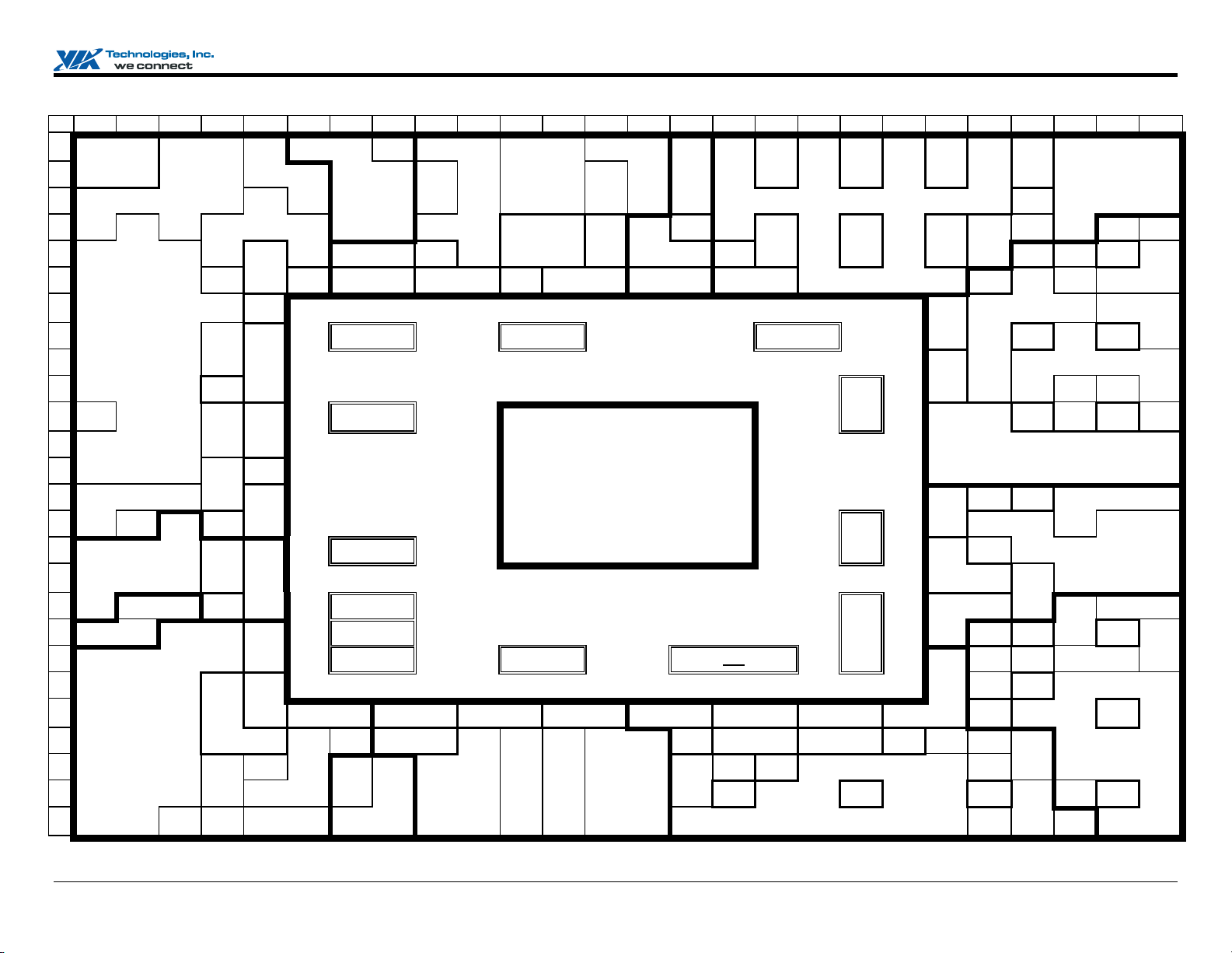
PINOUTS Figure 2. Ball Diagram (Top View)
Key 1 2 3 4 5 6 7 8 9 10 11 12 13 14 15 16 17 18 19 20 21 22 23 24 25 26
GPIO
GPIO
AGP
MRX
MRX
MTX
T
GND GND
A
GND GND
B
SERR# PERR# STOP#
C
CBE
D
E
F
G
H
J
K
L
M
N
P
R
T
U
V
W
Y
AA
AB
AC
AD
AE
AF
AD15 PAR
1#
AD11 AD13 AD14
AD10 AD9 AD12
AD7 AD6 AD4 AD8 GND
AD5 AD2 AD0
AD3 AD1 AD21
AD20 AD22 AD23 GND VCC
CBE
AD24 AD25
3#
AD27 AD26 AD28
AD29 AD31 AD30
INT
INT
A#
B#
INT
PCI
D#
RST#
AC
AC
SDO
AC
SDI3
MS
DT
CPU
MISS
EXT
SMI#
SUS
CLK
LID#
SMB
DT2
SMB
CK2
SUS
C#
AC
SDI0
AC
SDI2
KB
DT
MS
CK
RING#
SUS
A#
SMB
ALRT#
SMB
DT1
PWR
BTN#
PWR
OK#
SUS
B#
TRUD#
SYNC
CBE
RDY#
DEV
SEL#
RST#
BTCK
SDI1
PME#
SUS
GPO 0 VSUS
SMB
CK1
RTC
2#
FRM# AD16 AD19
RDY#
REQ
2#
GNT
2#
CBE
0#
REQ
3#
GNT
3#
REQ
4#
GNT
4#
REQ5#
GPI7
INT
GNT5#
C#
GPO7
AC
GND
AC
VSUS
25
AC
VSUS
25
KB
GND VCC
CK
BAT
LOW#
THRM#
ST#
33
VSUS
33
GPI 1 VSUS
33
IN
RTC
X1
GPI 0 V
BAT
PWR
X2
GD
AD17
I
REQ
1#
GNT
1#
VCC
33
VCC
33
VCC
VCC
VCC
33
VCC
33
GND
VCC
33
VCC
33
VCC
VCC
VCC
33
VCC
33
GND
GND
VSUS
33
RSM
RST#
GPIO A GPIO C L
PCK
RUN#
11
AD18
REQ
0#
GNT
0#
GND
12
BZ#
GPIO 9 GPIO
GPIO
GPIO
RAM
VCC
VCC
15
10
33
13
VGATE
GPIO8
GPIO
14
RAM
GND
VCC
33
D3
ERR
MD
MRX
IO
CLK
MD
MRX
CK
DV
MRX
MRX
D2
D1
MRX
GND
VCC VCC GND
D0
D1
MTX
D2
MTX
D3
MII
VCC
MII
VCC
MTX
CLK
MTX
ENA M CRS
MTX
VCC
VCC
VCC
G6 7 8 9 10 11 12 13 14 15 16 17 18 19 G20
H GPIO Pins LAN Pins USB Pins H
J J
K K11 12 13 14 15 K16 V-Link K
L PCI Pins L10 GND GND GND GND GND GND L17 Pins L
M M GND GND GND GND GND GND M M
N N GND GND GND GND GND GND N N
P P GND GND GND GND GND GND P P
R R GND GND GND GND GND GND R CPU R
T
AC97 Pins
U
U11 12 13 14 15 U16 U
T10 GND GND GND GND GND GND T17 Pins T
V KB/MS Pins Pri V
W PM Pins IDE W
Y LPC Pins X-Bus Pins Sec IDE Pins Pins Y
AA6 7 8 9 10 11 12 13 14 15 16 17 18 19 AA20
VCC
VCC
VCC
33
GPIO E CPU
GPIO D L
PCI
STP# L AD3 L AD0
VCC VCC
33
GND GND IOR#
STP#
REQ# L AD2
FRM# L AD1
IOW#
SPKR
strap
TEST
33
IO
RDY
SER
IRQ
MEM
W#
VCC
33
SA19
strap
SA18
strap
SA17
strap
SA16
strap
GND GND
OSC
SOE#
strap
MEM
ROMCS
#/strap
EE
CS#
D0 M COL
MII
MII
VCC25
MII
MII
VCC25
VCC
33
33
XD 1 XD 0 SD
XD 7 XD 4 SD
XD 6 XD 3 SD
R#
XD 5 XD 2 SDD0
EE
USB
DO
OC0#
EE
USB
DI
OC1#
EE
USB
CK
OC2#
USB
VSUS
OC4#
USB
USB
USB
OC5#
OC3#
VCC VCC
VCC
VCC
33
33
COMP
RDY
DRQ
SA00
USB
USB
USB
GND
P4+
USB
USB
GND
P4–
USB
USB
GND
GND
USB
USB
GND
P5–
USB
GND
P5+
VCC
VCC
33
33
VCC VCC GND GND
GND GND
SDD1
SA01
GND
SDD2
SA02
SD
VREF
SDD4
SA04
SDD3
SA03
GND
USB
GND
USB
GND
USB
GND
USB
GND
USB
GND
VCC
33
SDD5
SA05
SDD7
SA07
SDD6
SA06
USB
P2+
USB
P2–
USB
GND
USB
P3–
USB
P3+
USB
GND
VCC
33
SDD9
SA09
GND
SDD8
SA08
USB
GND
USB
GND
USB
GND
USB
GND
USB
GND
USB
GND
VCC
33
GND
SDD10
SA10
SDD12
SA12
SDD11
SA11
USB
USB
P0+
GND
USB
USB
P0–
GND
USB
USB
GND
GND
USB
VCC
P1–
UPLL
USB
GND
P1+
UPLL
USB
VCC
GND
GND
VCC
VCC
VCC
IOW#
SDD13
SA13
SDD15
SA15
SDD14
SA14
VK
VCC
VAD
VK
11
VCC
VAD
VK
12
VAD
VCC
VCC
VCC
VCC
VCC
VCC
VCC
VCC
VCC VCC
GND GND
VK
VK
VK
33
33
33
33
33
SD
14
VAD
15
VCC
VK
VCC
VK
VCC
VK
PLL
VCC
PCI
CLK
APIC
D0
PD
VREF
PD
DRQ
PD
D15
GND
SDA1
strap
SD
DAK#
GND
SD
IOR#
VCC
USB
UPLL
GND
UPLL
USB
REXT
USB
CLK
GND
VAD 9 VBE
VAD
10
GND
VL
VREF
VL
COMP
GND
VCC
VK
VCC
VK
PLL
GND
NMI GHI# INIT#
INTR SMI# A20M#
APIC
CLK
APIC
D1
PD
COMP
PD
A0
GND
PD
D12
SDCS1#
strap
SDCS3#
strap
SDA0
strap
SDA2
strap
USB
VCC
VCC
USB
USB
VCC
VCC
USB
USB
VCC
VCC
USB
VAD 8 V
VCC
VAD
GND
5
VAD 0 VAD
0#
VAD
DN
13
STB
UP
GND
STB
DN
VAD 3 VAD
CMD
VAD 6 UP
CMD
V
GND
CLK
VCC
VCC
VK
VK
VCC
VCC
VK
VK
VRD
VID
SLP
SEL
TPO SLP# FERR#
PD
PD
CS1#
CS3#
IOR#
PD
PD
PD
D0
PD
D2
PD
D4
PD
D9
IRQ
14
IRQ
15
A1
GND
PD
IOW#
PD
D1
GND
PD
D11
PD
D5
GND
PD
D7
USB
VCC
USB
VCC
USB
VCC
PAR
VAD
4
1
DN
STB#
UP
STB#
2
VAD
7
VBE
1#
VCC
VK
VCC
VK
DP
SLP#
STP
CLK#
IGN
NE#
PD
A2
PD
DAK#
PD
RDY
PD
D14
PD
D13
PD
D3
PD
D10
PD
D6
PD
D8
Revision 2.03, March 16, 2005 -6- Pin Diagram
Page 14
VT8235M Version CD V-Link South Bridge
Q
p
p
Q
Q
–
p
–
–
K
Q
Q
p
K
Q
p
Q
p
K
p
K
p
p
p
Q
K
Table 1. Pin List (Numerical Order)
Pin # Pin Name Pin # Pin Name Pin # Pin Name Pin # Pin Name Pin # Pin Name
A01 P GND
A02 P GND
A03 IO TRDY#
A04 IO CBE2# D01 IO CBE1#
A05 IO AD17 D02 IO AD15
A06 IO GPIO11 D03 IO PAR
A07 IO GPIO12 / INTE# / PCGNTA D04 I REQ2# H24 O UPSTB
A08 I AGPBZ# / GPI6 D05 O GNT1#
A09 I MRXD3 D06 I REQ0# H26 O UPSTB#
A10 I MRXERR D07 IO GPIO10
A11 O MTXD1 D08 IO GPIO14 / INTG#
A12 I MTXCLK D09 I MRXD2
A13 O EECS#
A14 I EEDO
A15 I USBOC0#
A16 P USBGND
A17 IO USBP4+ D14 I USBOC4# J25 IO VAD03 W22–NC AD20 IO SDD10 / SA10
A18 P USBGND D15 P VSUSUSB
A19 IO USBP2+
A20 P USBGND
A21 IO USBP0+
A22 P USBGND
A23 P VCCUPLL D20 P USBGND
A24 P USBVCC
A25 P USBVCC D22 P VCCUPLL
A26 P USBVCC
B01 P GND
B02 P GND
B03 IO DEVSEL#
B04 IO FRAME# E01 IO AD11 L03 IO AD25
B05 IO AD16 E02 IO AD13
B06 IO AD19 E03 IO AD14
B07 IO GPIO9 / PCREQB E04 O GNT2# L24 I VCL
B08 IO GPIO13 / INTF# / PCGNTB E06 O GNT0#
B09 IO MDIO
B10 I MRXCLK
B11 O MTXD2
B12 O MTXENA E10 I MRXD0
B13 I MCRS
B14 O EEDI
B15 I USBOC1# E13
B16 P USBGND
B17 IO USBP4– E15 I USBOC3# N04 I REQ5# / GPI7
B18 P USBGND
B19 IO USBP2– E17 IO USBP5+ P02 I INTB# AB23 IO PDD12
B20 P USBGND E18 P USBGND
B21 IO USBP0– E19 IO USBP3+ P04 O GNT5# / GPO7
B22 P USBGND E20 P USBGND P22 P PLLVCC
B23 P GNDUPLL
B24 P USBVCC E22 P GNDUPLL
B25 P USBVCC
B26 P USBVCC
C01 I SERR#
C02 IO PERR# E26 IO VAD04 R02 O PCIRST# AC06 IO GPIOE / GPIO31 AF05 IO PCKRUN#
C03 IO STOP#
C04 IO IRDY#
C05 I REQ1#
C06 IO AD18 F04 IO CBE0#
C07 IO GPIO15 / INTH#
C08 I VGATE / GPIO8 / PCREQA
C09 O MDCK
C10 I MRXDV
C11 O MTXD3 F23 IO VAD09
C12 O MTXD0 F24 IO VBE0#
C13 I MCOL F25 IO VAD00
C14 O EECK
C15 I USBOC2#
C16 P USBGND
C17 P USBGND
C18 P USBGND
C19 P USBGND
C20 P USBGND
C21 P USBGND
C22 P USBGND
C23 AI USBREXT
GND pins (28 pins): F6,11, G5, L11-16, M11-16, N5,11-16, P11-16, R11-16, T11-16, V21, W21, AA5, AB5,12-13,18-19
VCC pins (19 pins): F9-10,14-15, H5, J5,21, K5,21, T5,21, U5,21-22, V5, AB8-9,16-17
VCC33 pins (25 pins): F5,7-8,12-13,16-17, L5, M5, P5,21, R5,21, W5, Y5,21, AA21, AB6-7,10-11,14-15,20-21
VCCVK pins (17 pins): F22, G21, H21, L21-22, M21-26, N21-26
C24 P USBVCC
C25 P USBVCC
C26 P USBVCC
D10 I MRXD1 J04 O GNT3# W01 IO MSDT / IR
D11 P MIIVCC
D12 P MIIVCC J23 P VLVREF
D13
P MIIVCC25
D16 P USBGND
D17 IO USBP5
D18 P USBGND
D19 IO USBP3
D21 IO USBP1
D23 I USBCL
D24 P USBVCC
D25 IO VAD08
D26 IO VPAR
E07 P RAMVCC
E08 P RAMGND
E09 P GND
E11 P MIIVCC
E12 P MIIVCC
P MIIVCC25
E14 I USBOC5#
E16 P GND
E21 IO USBP1+
E23 P GND
E24 IO VAD05
E25 P GND
F01 IO AD10 R03 O ACRST# AC07 O CPUSTP# / GPO5
F02 IO AD09
F03 IO AD12
F18 P USBGND
F19 P USBGND
F20 P USBGND
F21 P USBGND
F26 IO VAD01
G01 IO AD07
G02 IO AD06
G03 IO AD04 T25 OD A20M#
G04 IO AD08
G22 IO VAD11
G23 IO VAD10
G24 IO VAD13
G25 I DNSTB
G26 I DNSTB# U23 I APICCL
K25 O UPCMD Y22 I PDDR
H01 IO AD05
H02 IO AD02
H03 IO AD00 U26 I FERR#
H04 I RE
H22 IO VAD12 V02 IO KBDT / KBRC AD08 IO LAD2
H23 P GND
H25 P GND V22 P GND
J01 IO AD03
J02 IO AD01
J03 IO AD21
J22 IO VAD14 W02 IO MSCK / IR
J24 I DNCMD W04 I BATLOW# / GPI5
J26 IO VAD02
K01 IO AD20
K02 IO AD22
K03 IO AD23
K04 P GND
K22 IO VAD15 Y02 I RING# / GPI3 AD26 IO PDD10
K23 I VLCOMP
K24 IO VAD06 Y04 I THRM# / GPI18 AE02 O PWROK#
K26 IO VAD07 Y23 O PDA0
L01 IO CBE3#
L02 IO AD24
L04 I RE
L23 P GND
L25 P GND
L26 IO VBE1# AA22 IO PDD15 AE12 IO MEMR#
M01 IO AD27
M02 IO AD26
M03 IO AD28
M04 O GNT4# AA26 IO PDD14
N01 IO AD29
N02 IO AD31
N03 IO AD30
P01 I INTA#
P03 I INTC# AB24 IO PDD02 AE23 O SDA0 / stra
P23 P PLLGND
P24 OD VRDPSLP / GPIO29 AC02 IO SMBDT1 AF01 O SUSC#
P25 OD VIDSEL / GPIO28 AC03 I GPI1 AF02 O SUSB# / GPO2
P26 OD DPSLP# / GPIO23
R01 I INTD#
R04 P GND
R22 I PCICL
R23 OD NMI AC10 IO IOR# AF09 I TEST
R24 OD GHI# / GPIO22
R25 OD INIT# AC12 I OSC AF11 IO SA16 / O16 / stra
R26 OD STPCLK# AC13 IO XD1 AF12 O ROMCS#/KBCS#/
T01 O ACSYNC
T02 I ACSDIN0
T03 I ACBITCL
T04 P VSUS25 AC17 P GND
T22 O APICD0
T23 OD INTR AC21 O SDIOW# AF18 IO SDD06 / SA06
T24 OD SMI# AC22 O SDA1 / stra
T26 OD IGNNE# AC24 IO PDD04 AF21 IO SDD14 / SA14
U01 O ACSDOUT
U02 I ACSDI2 /IO20/PCS0#
U03 I ACSDIN1
U04 P VSUS25
3#
4#
U24 O TPO AD04 I RTCX1
U25 OD SLP# AD05 I RSMRST#
V01 I ACSDI3 /IO21/PCS1# /SB#
V03 IO KBCK / A20G AD09 IO IOW#
V04 P GND
V23 O APICD1
V24 O PDCS1# AD13 IO XD7
V25 O PDA1 AD14 IO XD4
V26 O PDA2 AD15 I SDRDY
W03 I PME# AD18 IO SDD05 / SA05
W23 I PDCOMP
W24 O PDCS3# AD22 O SDDACK#
W25 P GND
W26 O PDDACK# AD24 IO PDD09
Y01 I CPUMISS / GPI17 AD25 IO PDD05
Y03 O SUSST1# / GPO3 AE01 IO SMBCK2 /
Y24 O PDIOR# AE05 IO GPIOA / GPIO24
Y25 O PDIOW# AE06 IO GPIOC / GPIO25
Y26 I PDRDY AE07 O LFRM#
AA01 IO EXTSMI# / GPI2
AA02 O SUSA# / GPO1 AE09 O SPKR / stra
AA03 OD GPO0 AE10 I SERIR
AA04 P VSUS33
AA23 P GND
AA24 IO PDD00 AE14 IO XD3
AA25 IO PDD01 AE15 I SDDR
AB01 O SUSCLK / GPO4 AE17 IO SDD04 / SA04
AB02 I SMBALRT# AE18 IO SDD07 / SA07
AB03 IO SMBCK1
AB04 P VSUS33
AB22 P GND
AB25 P GND
AB26 IO PDD13
AC01 I LID# / GPI4 AE26 IO PDD06
AC04 P VSUS33
AC05 P VSUS33
AC08 P GND
AC09 P GND
AC11 IO SA19 / O19 / strap AF10 IO MEMW#
AC14 IO XD0 AF13 IO XD5
AC15 I SDCOMP
AC16 P GND
AC20 P GND
AC23 O SDCS1# / stra
AC25 IO PDD11 AF22 O SDIOR#
AC26 IO PDD03 AF23 O SDA2 / stra
AD01 IO SMBDT2 / GPIO26 AF24 I IR
AD02 I PWRBTN# AF25 IO PDD07
AD03 I INTRUD# / GPI16 AF26 IO PDD08
12 AD16 IO SDD01 / SA01
1 AD17–NC
AF19 IO SDD08 / SA08
AF20 IO SDD11 / SA11
AD06 IO GPIOD / GPIO30
AD07 I LREQ#
AD10 I IORDY / GPI19
AD11 IO SA18 / O18 / stra
AD12 O SOE# / stra
AD19 IO SDD09 / SA09
AD21 IO SDD13 / SA13
AD23 O SDCS3# / stra
AE03 I GPI0
AE04 P VBAT
AE08 IO LAD1
AE11 IO SA17 / O17 / stra
AE13 IO XD6
AE16 P GND
AE19 P GND
AE20 IO SDD12 / SA12
AE21 IO SDD15 / SA15
AE22 P GND
AE24 I IRQ14
AE25 P GND
AF03 O RTCX2
AF04 I PWRGD
AF06 O PCISTP# / GPO6
AF07 IO LAD3
AF08 IO LAD0
AF14 IO XD2
AF15 IO SDD00 / SA00
AF16 IO SDD02 / SA02
AF17 IO SDD03 / SA03
15
Revision 2.03, March 16, 2005 -7- Pin Lists
Page 15
VT8235M Version CD V-Link South Bridge
K
p
p
p
p
Q
Q
–
K
–
–
–
–
–
–
–
K
Q
Q
Q
p
p
Q
Q
K
Q
Q
Q
Q
Q
Q
K
r
p
p
p
Table 2. Pin List (Alphabetical Order)
Pin # Pin Name Pin # Pin Name Pin # Pin Name Pin # Pin Name Pin # Pin Name
T25 OD A20M#
T03 I ACBITCLK
R03 O ACRST#
T02 I ACSDIN0
U03 I ACSDIN1
U02 I ACSDI2 /IO20/PCS0#
V01 I ACSDI3 /IO21/PCS1# /SLPB#
U01 O ACSDOUT
T01 O ACSYNC
H03 IO AD00
J02 IO AD01
H02 IO AD02
J01 IO AD03
G03 IO AD04
H01 IO AD05
G02 IO AD06
G01 IO AD07
G04 IO AD08
F02 IO AD09
F01 IO AD10
E01 IO AD11
F03 IO AD12
E02 IO AD13
E03 IO AD14
D02 IO AD15
B05 IO AD16
A05 IO AD17
C06 IO AD18
B06 IO AD19
K01 IO AD20
J03 IO AD21
K02 IO AD22
K03 IO AD23
L02 IO AD24
L03 IO AD25
M02 IO AD26
M01 IO AD27
M03 IO AD28
N01 IO AD29
N03 IO AD30
N02 IO AD31
A08 I AGPBZ# / GPI6 T26 OD IGNNE# AD26 IO PDD10 AA02 O SUSA# / GPO1 F23 IO VAD09
U23 I APICCLK
T22 O APICD0
V23 O APICD1
W04 I BATLOW# / GPI5
F04 IO CBE0#
D01 IO CBE1#
A04 IO CBE2#
L01 IO CBE3#
Y01 I CPUMISS / GPI17 AD10 I IORDY / GPI19 Y25 O PDIOW# K25 O UPCMD L26 IO VBE1#
AC07 O CPUSTP# / GPO5
B03 IO DEVSEL#
J24 I DNCMD
G25 I DNSTB
G26 I DNSTB#
P26 OD DPSLP# / GPIO23
C14 O EECK
A13 O EECS#
B14 O EEDI
A14 I EEDO
AA01 IO EXTSMI# / GPI2
U26 I FERR#
B04 IO FRAME#
R24 OD GHI# / GPIO22
A01 P GND
A02 P GND
B01 P GND
B02 P GND
E09 P GND
E16 P GND
E23 P GND
E25 P GND
H23 P GND
H25 P GND
GND pins (28 pins): F6,11, G5, L11-16, M11-16, N5,11-16, P11-16, R11-16, T11-16, V21, W21, AA5, AB5,12-13,18-19
VCC pins (19 pins): F9-10,14-15, H5, J5,21, K5,21, T5,21, U5,21-22, V5, AB8-9,16-17
VCC33 pins (25 pins): F5,7-8,12-13,16-17, L5, M5, P5,21, R5,21, W5, Y5,21, AA21, AB6-7,10-11,14-15,20-21
VCCVK pins (17 pins): F22, G21, H21, L21-22, M21-26, N21-26
K04 P GND
L23 P GND
L25 P GND
R04 P GND
V04 P GND
V22 P GND
W25 P GND
AA23 P GND
AB22 P GND
AB25 P GND
AC08 P GND
AC09 P GND
AC16 P GND
AC17 P GND
AC20 P GND
AE16 P GND
AE19 P GND
AE22 P GND
AE25 P GND
B23 P GNDUPLL
E22 P GNDUPLL
E06 O GNT0# AF05 IO PCKRUN# AF21 IO SDD14 / SA14 C23 AI USBREXT
D05 O GNT1# R22 I PCICL
E04 O GNT2# R02 O PCIRST# AD22 O SDDACK#
J04 O GNT3# AF06 O PCISTP# / GPO6 AE15 I SDDR
M04 O GNT4# Y23 O PDA0 AF22 O SDIOR#
P04 O GNT5# / GPO7 V25 O PDA1 AC21 O SDIOW#
AE03 I GPI0 V26 O PDA2 AD15 I SDRDY
AC03 I GPI1
B07 IO GPIO9 / PCRE
D07 IO GPIO10 W24 O PDCS3# U25 OD SLP#
A06 IO GPIO11 AA24 IO PDD00 AB02 I SMBALRT#
A07 IO GPIO12/INTE#/PCGA AA25 IO PDD01 AB03 IO SMBCK1 F25 IO VAD00
B08 IO GPIO13/INTF#/PCGB AB24 IO PDD02 AE01 IO SMBCK2 / GPIO27 F26 IO VAD01
D08 IO GPIO14 / INTG# AC26 IO PDD03 AC02 IO SMBDT1 J26 IO VAD02
C07 IO GPIO15 / INTH# AC24 IO PDD04 AD01 IO SMBDT2 / GPIO26 J25 IO VAD03
AE05 IO GPIOA / GPIO24 AD25 IO PDD05 T24 OD SMI# E26 IO VAD04
AE06 IO GPIOC / GPIO25 AE26 IO PDD06 AD12 O SOE# / stra
AD06 IO GPIOD / GPIO30 AF25 IO PDD07 AE09 O SPKR / stra
AC06 IO GPIOE / GPIO31 AF26 IO PDD08 C03 IO STOP# K26 IO VAD07
AA03 OD GPO0 AD24 IO PDD09 R26 OD STPCLK# D25 IO VAD08
R25 OD INIT# AC25 IO PDD11 AF02 O SUSB# / GPO2 G23 IO VAD10
P01 I INTA# AB23 IO PDD12 AF01 O SUSC# G22 IO VAD11
P02 I INTB# AB26 IO PDD13 AB01 O SUSCLK / GPO4 H22 IO VAD12
P03 I INTC# AA26 IO PDD14 Y03 O SUSST1# / GPO3 G24 IO VAD13
R01 I INTD# AA22 IO PDD15 AF09 I TEST J22 IO VAD14
T23 OD INTR W26 O PDDACK# Y04 I THRM# / GPI18 K22 IO VAD15
AD03 I INTRUD# / GPI16 Y22 I PDDR
AC10 IO IOR# Y24 O PDIOR# A03 IO TRDY# F24 IO VBE0#
AD09 IO IOW# Y26 I PDRDY H24 O UPSTB
C04 IO IRDY# C02 IO PERR# H26 O UPSTB#
AE24 I IR
AF24 I IR
V03 IO KBCK / A20G W03 I PME#
V02 IO KBDT / KBRC AD02 I PWRBTN#
AF08 IO LAD0 AF04 I PWRGD
AE08 IO LAD1 AE02 O PWROK#
AD08 IO LAD2
AF07 IO LAD3
AE07 O LFRM# D06 I RE
AC01 I LID# / GPI4 C05 I RE
AD07 I LRE
C13 I MCOL H04 I RE
B13 I MCRS L04 I RE
C09 O MDC
B09 IO MDIO Y02 I RING# / GPI3
AE12 IO MEMR# AF12 O ROMCS#/KBCS#/st
AF10 IO MEMW# AD05 I RSMRST#
D11 P MIIVCC
D12 P MIIVCC
E11 P MIIVCC
E12 P MIIVCC
D13
14
15
# D04 I REQ2#
N04 I REQ5# / GPI7
P MIIVCC25
E13
P MIIVCC25
B10 I MRXCL
E10 I MRXD0 AC22 O SDA1 / stra
D10 I MRXD1 AF23 O SDA2 / stra
D09 I MRXD2
A09 I MRXD3 AC23 O SDCS1# / stra
C10 I MRXDV AD23 O SDCS3# / stra
A10 I MRXERR AF15 IO SDD00 / SA00 D14 I USBOC4#
W02 IO MSCK / IR
W01 IO MSDT / IR
A12 I MTXCL
C12 O MTXD0 AE17 IO SDD04 / SA04 D21 IO USBP1
A11 O MTXD1 AD18 IO SDD05 / SA05 E21 IO USBP1+
B11 O MTXD2 AF18 IO SDD06 / SA06 B19 IO USBP2
C11 O MTXD3 AE18 IO SDD07 / SA07 A19 IO USBP2+
B12 O MTXENA AF19 IO SDD08 / SA08 D19 IO USBP3
W22
AD17
R23 OD NMI AF20 IO SDD11 / SA11 A17 IO USBP4+
AC12 I OSC AE20 IO SDD12 / SA12 D17 IO USBP5
D03 IO PAR AD21 IO SDD13 / SA13 E17 IO USBP5+
W23 I PDCOMP
B V24 O PDCS1# C01 I SERR#
P23 P PLLGND
P22 P PLLVCC A16 P USBGND
E08 P RAMGND B18 P USBGND
E07 P RAMVCC B20 P USBGND T04 P VSUS25
AD04 I RTCX1
AF03 O RTCX2
AF11 IO SA16 / O16 / stra
AE11 IO SA17 / O17 / stra
AD11 IO SA18 / O18 / stra
NC AD19 IO SDD09 / SA09 E19 IO USBP3+
NC AD20 IO SDD10 / SA10 B17 IO USBP4
0#
1#
3#
4#
AC11 IO SA19 / O19 / strap
AE23 O SDA0 / strap
AC15 I SDCOMP
1 AD16 IO SDD01 / SA01 E14 I USBOC5#
12 AF16 IO SDD02 / SA02 B21 IO USBP0
AF17 IO SDD03 / SA03 A21 IO USBP0+
AE21 IO SDD15 / SA15
AE10 I SERIR
U24 O TPO
D23 I USBCLK L24 I VCL
A18 P USBGND
A20 P USBGND K23 I VLCOMP
A22 P USBGND J23 P VLVREF
B16 P USBGND
B22 P USBGND U04 P VSUS25
C16 P USBGND AA04 P VSUS33
C17 P USBGND AB04 P VSUS33
C18 P USBGND AC04 P VSUS33
C19 P USBGND AC05 P VSUS33
C20 P USBGND D15 P VSUSUSB
C21 P USBGND
C22 P USBGND
D16 P USBGND
D18 P USBGND
D20 P USBGND
E18 P USBGND
E20 P USBGND
F18 P USBGND
F19 P USBGND
F20 P USBGND
F21 P USBGND
A15 I USBOC0#
B15 I USBOC1#
C15 I USBOC2#
E15 I USBOC3#
A24 P USBVCC
A25 P USBVCC
A26 P USBVCC
B24 P USBVCC
B25 P USBVCC
B26 P USBVCC
C24 P USBVCC
C25 P USBVCC
C26 P USBVCC
D24 P USBVCC
E24 IO VAD05
K24 IO VAD06
AE04 P VBAT
A23 P VCCUPLL
D22 P VCCUPLL
C08 I VGATE/GPIO8/PCRA
P25 OD VIDSEL / GIO28
D26 IO VPAR
P24 OD VRDPSLP/GPIO29
AC14 IO XD0
AC13 IO XD1
AF14 IO XD2
AE14 IO XD3
AD14 IO XD4
AF13 IO XD5
AE13 IO XD6
AD13 IO XD7
Revision 2.03, March 16, 2005 -8- Pin Lists
Page 16
VT8235M Version CD V-Link South Bridge
PIN DESCRIPTIONS
V-Link Pin Descriptions
V-Link Interface
Signal Name Pin # I/O Signal Description
VAD[15:0]
VPAR
VBE[1:0]#
VCLK
UPCMD
DNCMD
UPSTB
UPSTB#
DNSTB
DNSTB#
VLCOMP
K22, J22, G24, H22,
G22, G23, F23, D25,
K26, K24, E24, E26,
J25, J26, F26, F25
D26 IO Parity. If the VPAR function is implemented in a compatible manner on the
L26, F24 IO Byte Enables. VBE0# is used with VAD[7-0] and VBE1# is used with
L24 I
K25 O
J24 I
H24 O
H26 O
G25 I
G26 I
K23 AI
IO Address / Data Bus. Bits 0-7 are implemented and bits 8-15 are reserved for
future use. VAD[7:0] are used to send strap information to the chipset north
bridge. At power up VAD7 reflects the state of a strap on SDCS3#,
VAD[6:4] reflect the state of straps on pins SDA[2:0] and VAD[3:0] reflect
the state of straps on pins SA[19:16]. The specific interpretation of these
straps is north bridge chip design dependent.
north bridge, this pin should be connected to the north bridge VPAR pin
(P4X333, P4X400, P4X800, KT400). If VPAR is not implemented in the
north bridge chip or is incompatible with the 8235 (4x V-Link north bridges)
connect this pin to an 8.2K pullup to 2.5V (Pro266, Pro266T, KT266,
KT266A, KT333, P4X266, PN266, KN266, KM266, P4M266, P4N266). See
app note AN222 for details.
VAD[15-8] (VBE1# and VAD[15-8] are reserved for future use).
V-Link Clock.
Command from Client-to-Host.
Command from Host-to-Client.
Strobe from Client-to-Host.
Complement Strobe from Client-to-Host.
Strobe from Host-to-Client.
Complement Strobe from Host-to-Client.
V-Link Compensation.
Revision 2.03, March 16, 2005 -9- Pin Descriptions
Page 17
VT8235M Version CD V-Link South Bridge
CPU, APIC and CPU Control Pin Descriptions
CPU Interface
Signal Name Pin # I/O Signal Description
A20M#
FERR#
IGNNE#
INIT#
INTR
NMI
SLP#
SMI#
STPCLK#
Note: Connect each of the above signals to 150 Ω pullup resistors to VCC_CMOS (see Design Guide).
T25 OD A20 Mask. Connect to A20 mask input of the CPU to control address bit-20 generation.
Logical combination of the A20GATE input (from internal or external keyboard controller)
and Port 92 bit-1 (Fast_A20).
U26 I Numerical Coprocessor Error. This signal is tied to the coprocessor error signal on the
CPU. Internally generates interrupt 13 if active. Output voltage swing is programmable tot
1.5V or 2.5V by Device 17 Function 0 Rx67[2].
T26 OD Ignore Numeric Error. This pin is connected to the CPU “ignore error” pin.
R25 OD Initialization. The VT8235M Version CD asserts INIT# if it detects a shut-down special
cycle on the PCI bus or if a soft reset is initiated by the register
T23 OD CPU Interrupt. INTR is driven by the VT8235M Version CD to signal the CPU that an
interrupt request is pending and needs service.
R23 OD Non-Maskable Interrupt. NMI is used to force a non-maskable interrupt to the CPU. The
VT8235M Version CD generates an NMI when PCI bus SERR# is asserted.
U25 OD Sleep. Used to put the CPU to sleep.
T24 OD System Management Interrupt. SMI# is asserted by the VT8235M Version CD to the
CPU in response to different Power-Management events.
R26 OD Stop Clock. STPCLK# is asserted by the VT8235M Version CD to the CPU to throttle the
processor clock.
Advanced Programmable Interrupt Controller (APIC) Interface
Signal Name Pin # I/O Signal Description
APICD1
APICD0
APICCLK
V23 O Internal APIC Data 1. Function 0 Rx58[6] = 1
T22 O Internal APIC Data 0. Function 0 Rx58[6] = 1
U23 I
APIC Clock.
CPU Speed Control Interface
Signal Name Pin # I/O Signal Description
VGATE / GPI8
/ GPO8
/ PCREQA
VIDSEL / GPI2
/ GPO2
VRDSLP / GPI29
/ GPO29
GHI# / GPI22
/ GPO22
DPSLP# / GPI23
/ GPO23
CPUMISS / GPI17 Y1 I CPU Missing. Used to detect the physical presence of the CPU chip in its socket. High
AGPBZ# / GPI6 A8 I AGP Busy. Low indicates that an AGP master cycle is in progress (CPU speed transitions
C8 I Voltage Gate. Signal from the CPU voltage regulator. High indicates the voltage regulator
output is stable. This pin performs the VGATE function if Device 17 Function 0 Rx53[7] =
0, E5[4] = 1 and E4[3] = 0.
P25 OD Voltage Regulator ID Select. Connected to the CPU voltage regulator. Low selects the
voltage ID from the CPU; high selects a different fixed voltage ID (the lower voltage used
for CPU deep sleep mode). This pin performs the VIDSEL function if Func 0 RxE5[3] = 0.
P24 OD Voltage Regulator Deep Sleep. Connected to the CPU voltage regulator. High selects
the proper voltage for deep sleep mode. This pin performs the VRDPSLP function if
Function 0 RxE5[3] = 0.
R24 OD CPU Speed Select. Connected to the CPU voltage regulator, used to select high speed (L)
or low speed (H). This pin performs the GHI# function if Function 0 RxE5[3] = 0.
P26 OD CPU Deep Sleep. This pin performs the DPSLP# function if Device 17 Function 0
RxE5[3]=0.
indicates no CPU present. Connect to the CPUMISS pin of the CPU socket. The state of
this pin may be read in the SMBus 2 registers. This pin may be used as CPUMISS and
GPI17 at the same time.
will be postponed if this input is asserted low). Connected to the AGP Bus AGPBZ# pin.
Revision 2.03, March 16, 2005 -10- Pin Descriptions
Page 18
VT8235M Version CD V-Link South Bridge
PCI Bus Interface
Signal Name Pin # I/O Signal Description
AD[31:0]
CBE[3:0]#
DEVSEL#
FRAME#
IRDY#
TRDY#
STOP#
SERR#
PAR
INTA#
INTB#
INTC#
INTD#
INTE# / GPI12,
/ GPO12,
/ PCGNTA,
INTF# / GPI13,
/ GPO13,
/ PCGNTB,
INTG# / GPI14
/ GPO14,
INTH# / GPI15
/ GPO15
REQ5# / GPI7,
REQ4#,
REQ3#,
REQ2#,
REQ1#,
REQ0#
GNT5# / GPO7,
GNT4#,
GNT3#,
GNT2#,
GNT1#,
GNT0#
PCIRST#
PCICLK
PCKRUN#
(see pin
L1, A4,
D1, F4
,
,
list)
B3 IO Device Select. The VT8235M Version CD asserts this signal to claim PCI transactions
B4 IO Frame. Assertion indicates the address phase of a PCI transfer. Negation indicates that
C4 IO Initiator Ready. Asserted when the initiator is ready for data transfer.
A3 IO Target Ready. Asserted when the target is ready for data transfer.
C3 IO Stop. Asserted by the target to request the master to stop the current transaction.
C1 I System Error. SERR# can be pulsed active by any PCI device that detects a system error
D3 IO Parity. A single parity bit is provided over AD[31:0] and C/BE[3:0]#.
P1,
P2,
P3,
R1
A7,
B8,
D8,
C7
N4
L4
H4
D4
C5
D6
P4
M4
J4
E4
D5
E6
R2 O PCI Reset. This signal is used to reset devices attached to the PCI bus.
R22 I PCI Clock. This signal provides timing for all transactions on the PCI Bus.
AF5 IO PCI Bus Clock Run. This signal indicates whether the PCI clock is or will be stopped
IO Address / Data Bus. Multiplexed address and data. The address is driven with FRAME#
assertion and data is driven or received in following cycles.
IO Command / Byte Enable. The command is driven with FRAME# assertion. Byte
enables corresponding to supplied or requested data are driven on following clocks.
through positive or subtractive decoding. As an input, DEVSEL# indicates the response
to a VT8235M Version CD-initiated transaction and is also sampled when decoding
whether to subtractively decode the cycle.
one more data transfer is desired by the cycle initiator.
condition. Upon sampling SERR# active, the VT8235M Version CD can be programmed
to generate an NMI to the CPU.
I PCI Interrupt Request. The INTA# through INTD# pins are typically connected to the
PCI bus INTA#-INTD# pins per the table below. INTE-H# are enabled by setting Device
17, Function 0 Rx5B[1] = 1. BIOS settings must match the physical connection method.
INTA#
PCI Slot 1 INTA# INTB# INTC# INTD#
PCI Slot 2 INTB# INTC# INTD# INTE#
PCI Slot 3 INTC# INTD# INTE# INTF#
PCI Slot 4 INTD# INTE# INTF# INTG#
PCI Slot 5 INTE# INTF# INTG# INTH#
PCI Slot 6 INTF# INTG# INTH# INTA#
I PCI Request. These signals connect to the VT8235M Version CD from each PCI slot (or
each PCI master) to request the PCI bus. To use pin N4 as REQ5#, Function 0 RxE4 must
be set to 1 otherwise this pin will function as General Purpose Input 7.
O PCI Grant. These signals are driven by the VT8235M Version CD to grant PCI access to
a specific PCI master. To use pin P4 as GNT5#, Function 0 RxE4 must be set to 1
otherwise this pin will function as General Purpose Output 7.
(high) or running (low). The VT8235M Version CD drives this signal low when the PCI
clock is running (default on reset) and releases it when it stops the PCI clock. External
devices may assert this signal low to request that the PCI clock be restarted or prevent it
from stopping. Connect this pin to ground using a 100 Ω resistor if the function is not
used. Refer to the “PCI Mobile Design Guide” and an applicable VIA North Bridge
Design Guide (e.g., KT400, CLE266, or P4X400) for more details.
INTB# INTC# INTD#
Revision 2.03, March 16, 2005 -11- Pin Descriptions
Page 19
VT8235M Version CD V-Link South Bridge
MII, Serial EEPROM, LPC and DMA Pin Descriptions
LAN Controller - Media Independent Interface (MII)
Signal Name Pin # I/O PU Signal Description
MCOL
MCRS
MDCK
MDIO
MRXCLK
MRXD[3-0]
MRXDV
MRXERR
MTXCLK
MTXD[3-0]
MTXENA
MIIVCC
MIIVCC25
RAMVCC
RAMGND
C13 I
B13 I
C9 O
B9 IO
B10 I
A9, D9, D10, E10 I
C10 I
A10 I
A12 I
C11, B11, A11, C12 O
B12 O
D11, D12, E11, E12
D13, E13
E7
E8
Power
Power
Power
Power Ground For Internal LAN RAM.
MII Collision Detect. From the external PHY.
PD
MII Carrier Sense. Asserted by the external PHY when the media is
PD
active.
MII Management Data Clock. Sent to the external PHY as a timing
PD
reference for MDIO
MII Management Data I/O. Read from the MDI bit or written to the
PD
MDO bit.
MII Receive Clock. 2.5 or 25 MHz clock recovered by the PHY.
PD
MII Receive Data. Parallel receive data lines driven by the external
PD
PHY synchronous with MRXCLK.
PD MII Receive Data Valid.
MII Receive Error. Asserted by the PHY when it detects a data
PD
decoding error.
MII Transmit Clock. Always active 2.5 or 25 MHz clock supplied by
PD
the PHY.
MII Transmit Data. Parallel transmit data lines synchronized to
PD
MTXCLK.
MII Transmit Enable. Signals that transmit is active from the MII
PD
port to the PHY.
MII Interface Power. 3.3V ±5%.
MII Suspend Power. 2.5V ±5%.
Power For Internal LAN RAM. 2.5V ±5%.
Serial EEPROM Interface
Signal Name Pin # I/O PU Signal Description
EECS#
EECK
EEDO
EEDI
These pins are disabled if the SDCS1# pin is strapped low to enable serial EEPROM connection via the MII interface.
A13 O
C14 O
Serial EEPROM Chip Select.
Serial EEPROM Clock.
A14 I Serial EEPROM Data Output. Connect to EEPROM Data Out pin.
B14 O Serial EEPROM Data Input. Connect to EEPROM Data In pin.
Low Pin Count (LPC) Interface
Signal Name Pin # I/O PU Signal Description
LFRM#
LREQ#
LAD[3-0]
Note: Connect the LPC interface LPCRST# (LPC Reset) signal to PCIRST#
AF7, AD8, AE8, AF8 IO PU
AE7 O
AD7 I
LPC Frame.
LPC DMA / Bus Master Request.
LPC Address / Data.
PC / PCI DMA
Signal Name Pin # I/O PU Signal Description
PCREQA / GPI8 / GPO8
/ VGATE
PCREQB / GPI9 / GPO9 B7 I PC / PCI Request B. Device 17 Function 0 Rx53[7] = 1
PCGNTA / GPI12 / GPO12 A7 O PC / PCI Grant A. Device 17 Function 0 Rx53[7] = 1
PCGNTB / GPI13 / GPO13 B8 O PC / PCI Grant B. Device 17 Function 0 Rx53[7] = 1
C8 I PC / PCI Request A. Device 17 Function 0 Rx53[7] = 1
Revision 2.03, March 16, 2005 -12- Pin Descriptions
Page 20
VT8235M Version CD V-Link South Bridge
USB, SMB and Programmable Chip Select Pin Descriptions
Universal Serial Bus 2.0 Interface
Signal Name Pin # I/O Signal Description
USBP0+
USBP0–
USBP1+
USBP1–
USBP2+
USBP2–
USBP3+
USBP3–
USBP4+
USBP4–
USBP5+
USBP5–
USBCLK
USBREXT
USBOC0#
USBOC1#
USBOC2#
USBOC3#
USBOC4#
USBOC5#
USBVCC
USBGND
VSUSUSB
VCCUPLL
GNDUPLL
A21 IO
B21 IO
E21 IO
D21 IO
A19 IO
B19 IO
E19 IO
D19 IO
A17 IO
B17 IO
E17 IO
D17 IO
D23 I USB 2.0 Clock. 48MHz clock input for the USB interface
C23 AI
A15 I USB 2.0 Port 0 Over Current Detect. Port 0 is disabled if low.
B15 I USB 2.0 Port 1 Over Current Detect. Port 1 is disabled if low.
C15 I USB 2.0 Port 2 Over Current Detect. Port 2 is disabled if low.
E15 I USB 2.0 Port 3 Over Current Detect. Port 3 is disabled if low.
D14 I USB 2.0 Port 4 Over Current Detect. Port 4 is disabled if low.
E14 I USB 2.0 Port 5 Over Current Detect. Port 5 is disabled if low.
(see pin list)
(see pin list)
D15
A23, D22
B23, E22
Power
Power USB 2.0 Port Differential Output Interface Logic Ground.
Power
Power
Power USB 2.0 PLL Analog Ground.
USB 2.0 Port 0 Data +
USB 2.0 Port 0 Data –
USB 2.0 Port 1 Data +
USB 2.0 Port 1 Data –
USB 2.0 Port 2 Data +
USB 2.0 Port 2 Data –
USB 2.0 Port 3 Data +
USB 2.0 Port 3 Data –
USB 2.0 Port 4 Data +
USB 2.0 Port 4 Data –
USB 2.0 Port 5 Data +
USB 2.0 Port 5 Data –
USB External Resistor.
USB 2.0 Port Differential Output Interface Logic Voltage. 3.3V
USB 2.0 Suspend Power. 2.5V ±5%.
USB 2.0 PLL Analog Voltage. 2.5V ±5%.
System Management Bus (SMB) Interface (I2C Bus)
Signal Name Pin # I/O Signal Description
SMBCK1
SMBCK2 / GPI27 / GPO27 AE1 IO SMB / I2C Channel 2 Clock. Rx95[2] = 0
SMBDT1
SMBDT2 / GPI26 / GPO26 AD1 IO SMB / I2C Channel 2 Data. Rx95[2] = 0
SMBALRT#
AB3 IO
AC2 IO
AB2 I SMB Alert. (enabled by System Management Bus I/O space Rx08[3] =
SMB / I2C Channel 1 Clock.
SMB / I2C Channel 1 Data.
1) When the chip is enabled to allow it, assertion generates an IRQ or
SMI interrupt or a power management resume event. Connect to a 10K
ohm pullup to VSUS33 if not used.
Programmable Chip Selects
Signal Name Pin # I/O Signal Description
PCS0# / GPIO20 / ACSDIN2 U2 O Programmable Chip Select 0. RxE4[6]=1, E5[1]=1
PCS1# / GPIO21 / ACSDIN3 / SLPBTN# V1 O Programmable Chip Select 1. RxE4[6]=1, E5[2]=1
Revision 2.03, March 16, 2005 -13- Pin Descriptions
Page 21
VT8235M Version CD V-Link South Bridge
EIDE Interface Pin Descriptions
UltraDMA-133 / 100 / 66 / 33 Enhanced IDE Interface
Signal Name Pin # I/O Signal Description
PDRDY /
PDDMARDY /
PDSTROBE
SDRDY /
SDDMARDY /
SDSTROBE
PDIOR# /
PHDMARDY /
PHSTROBE
SDIOR# /
SHDMARDY /
SHSTROBE
PDIOW# /
PSTOP
SDIOW# /
SSTOP
PDDRQ
SDDRQ
PDDACK#
SDDACK#
IRQ14
IRQ15
Y26 I EIDE Mode: Primary I/O Channel Ready. Device ready indicator
UltraDMA Mode: Primary Device DMA Ready. Output flow control. The device may
assert DDMARDY to pause output transfers
Primary Device Strobe. Input data strobe (both edges). The device
may stop DSTROBE to pause input data transfers
AD15 I EIDE Mode: Secondary I/O Channel Ready. Device ready indicator
UltraDMA Mode: Secondary Device DMA Ready. O
may assert DDMARDY to pause output transfers
Secondary Device Strobe. Input data strobe (both edges). The device
may stop DSTROBE to pause input data transfers
Y24 O EIDE Mode: Primary Device I/O Read. Device read strobe
UltraDMA Mode: Primary Host DMA Ready. Primary
host may assert HDMARDY to pause input transfers
Primary Host Strobe. Output data strobe (both edges). The host may
stop HSTROBE to pause output data transfers
AF22 O EIDE Mode: Secondary Device I/O Read. Device read strobe
UltraDMA Mode: Secondary Host DMA Ready. Input flow control. The host may
assert HDMARDY to pause input transfers
Host Strobe B. Output strobe (both edges). The host may stop
HSTROBE to pause output data transfers
Y25 O EIDE Mode: Primary Device I/O Write. Device write strobe
UltraDMA Mode: Primary Stop. Stop transfer: Asserted by the host prior to initiation of
an UltraDMA burst; negated by the host before data is transferred in
an UltraDMA burst. Assertion of STOP by the host during or after data
transfer in UltraDMA mode signals the termination of the burst.
AC21 O EIDE Mode: Secondary Device I/O Write. Device write strobe
UltraDMA Mode: Secondary Stop. Stop transfer: Asserted by the host prior to initiation
of an UltraDMA burst; negated by the host before data is transferred in
an UltraDMA burst. Assertion of STOP by the host during or after data
transfer in UltraDMA mode signals the termination of the burst.
Y22 I Primary Device DMA Request. Primary
AE15 I Secondary Device DMA Request. Secondary
W26 O Primary Device DMA Acknowledge. Primary
AD22 O Secondary Device DMA Acknowledge. Secondary
AE24 I
AF24 I
Primary Channel Interrupt Request.
Secondary Channel Interrupt Request.
channel DMA request
channel DMA request
channel DMA acknowledge
utput flow control. The device
channel input flow control. The
channel DMA acknowledge
Revision 2.03, March 16, 2005 -14- Pin Descriptions
Page 22
VT8235M Version CD V-Link South Bridge
UltraDMA-133 / 100 / 66 / 33 Enhanced IDE Interface (continued)
Signal Name Pin # I/O Signal Description
PDCS1#
PDCS3#
SDCS1# / strap AC23 O Secondary Master Chip Select. This signal corresponds to CS17X#
SDCS3# / strap AD23 O Secondary Slave Chip Select. This signal corresponds to CS37X# on
PDA[2-0]
SDA[2-0] / strap AF23, AC22, AE23 O Secondary Disk Address. SDA[2:0] are used to indicate which byte in
PDD[15-0]
SDD[15-0] / SA[15-0] (see pin list) IO / IO
PDCOMP
SDCOMP
V24 O Primary Master Chip Select. This signal corresponds to CS1FX# on
the primary IDE connector.
W24 O Primary Slave Chip Select. This signal corresponds to CS3FX# on
the primary IDE connector.
on the secondary IDE connector. Strap low (resistor to ground) to
enable serial EEPROM interface via the MII bus (this disables the
EExx pins). This pin has an internal pullup to default to serial
EEPROM interface via the EExx pins.
the secondary IDE connector. Strap information is communicated to
the north bridge via VAD[7].
V26, V25, Y23 O Primary Disk Address. PDA[2:0] are used to indicate which byte in
either the ATA command block or control block is being accessed.
either the ATA command block or control block is being accessed.
Strap information is communicated to the north bridge via VAD[6:4].
(see pin list) IO
W23 I
AC15 I
Primary Disk Data.
Secondary Disk Data.
Primary Disk Compensation.
Secondary Disk Compensation.
Serial IRQ and AC97 Pin Descriptions
Serial IRQ
Signal Name Pin # I/O Signal Description
SERIRQ
AE10 I Serial IRQ. This pin has an internal pull-up resistor.
AC97 Audio / Modem Interface
Signal Name Pin # I/O Signal Description
ACRST#
ACBTCK
ACSYNC
ACSDO
ACSDIN0 (VSUS33)† T2 I
ACSDIN1 (VSUS33)† U3 I
ACSDIN2 / GPIO20 / PCS0# U2 I AC97 Serial Data In 2. RxE4[6]=0,E5[1]=0, PMIO Rx4C[20]=1
ACSDIN3 / GPIO21 / PCS1# / SLPBTN# V1 I AC97 Serial Data In 3. RxE4[6]=0,E5[2]=0, PMIO Rx4C[21]=1
†The supply voltage for ACSDIN0-1 is VSUS33 so these inputs can support wake-up on modem ring.
R3 O
T3 I
T1 O
U1 O
AC97 Reset.
AC97 Bit Clock.
AC97 Sync.
AC97 Serial Data Out.
AC97 Serial Data In 0.
AC97 Serial Data In 1.
Revision 2.03, March 16, 2005 -15- Pin Descriptions
Page 23
VT8235M Version CD V-Link South Bridge
Internal Keyboard Controller and Speaker Pin Descriptions
Internal Keyboard Controller
Signal Name Pin # I/O PU Signal Description
MSCK / IRQ1 W2 IO / I PU MultiFunction Pin (Internal mouse controller enabled by Rx51[1])
Rx51[2]=1 Mouse Clock. From internal mouse controller.
Rx51[2]=0 Interrupt Request 1. Interrupt input 1.
MSDT / IRQ12 W1 IO / I PU MultiFunction Pin (Internal mouse controller enabled by Rx51[1])
Rx51[2]=1 Mouse Data. From internal mouse controller.
Rx51[2]=0 Interrupt Request 12. Interrupt input 12.
KBCK / KA20G V3 IO / I PU MultiFunction Pin (Internal keyboard controller enabled by
Rx51[0])
Rx51[0]=1 Keyboard Clock. From internal keyboard controller
Rx51[0]=0 Gate A20. Input from external keyboard controller.
KBDT / KBRC V2 IO / I PU MultiFunction Pin (Internal keyboard controller enabled by
Rx51[0])
Rx51[0]=1 Keyboard Data. From internal keyboard controller.
Rx51[0]=0 Keyboard Reset. From external keyboard controller
(KBC) for CPURST# generation
KBCS# / ROMCS# / strap AF12 O / O Keyboard Chip Select (Rx51[0]=0). To external keyboard
controller chip. Strap high to enable LPC ROM:
Note: KBCK, KBDT, MSCK, and MSDT are powered by the VSUS33 suspend voltage plane.
ISA Subset / Parallel BIOS ROM Interface
Signal Name Pin # I/O PU Signal Description
ROMCS# / KBCS# /
strap
SPKR / strap AE9 O Speaker. Strap low to enable (high to disable) CPU frequency
MEMR#
MEMW#
IOR#
IOW#
IORDY / GPI19 AD10 I I/O Ready. Used to insert wait states in I/O or memory cycles.
SOE# / strap AD12 O XD Bus Tranceiver Output Enable. Strap low to enable auto
XD[7-0]
SA[19-16] / GPO[19-16]
/ straps
SA[15-0] / SDD[15-0] (see pin list) O
AF12 O ROM Chip Select (Rx51[0]=1). Chip Select to the BIOS ROM.
Strap high to enable LPC ROM.
strapping.
AE12 O
AF10 O
AC10 O
AD9 O
AD13, AE13,
AF13, AD14,
AE14, AF14,
AC13, AC14
AC11, AD11,
AE11, AF11
IO XD Bus. For input of BIOS ROM data or data from other on-board
O
Memory Read.
Memory Write.
I/O Read.
I/O Write.
RxE5[0] = 0
reboot.
I/O or memory devices.
System Address 19-16. Strap states are passed to North Bridge via
PD
VAD[3-0]. Functions as SA[19-16] if RxE4[5] = 0.
System Address 15-0.
Revision 2.03, March 16, 2005 -16- Pin Descriptions
Page 24
VT8235M Version CD V-Link South Bridge
General Purpose Input Pin Descriptions
General Purpose Inputs
Signal Name Pin # I/O Signal Description
GPI0 (VBAT)
GPI1 (VSUS33)
GPI2 / EXTSMI# (VSUS33) AA1 I General Purpose Input 2. Status on PMIO Rx20[4]
GPI3 / RING# (VSUS33) Y2 I General Purpose Input 3. Status on PMIO Rx20[8]
GPI4 / LID# (VSUS33) AC1 I General Purpose Input 4. Status on PMIO Rx20[11]
GPI5 / BATLOW# (VSUS33) W4 I General Purpose Input 5. Status on PMIO Rx20[12]
GPI6 / AGPBZ# A8 I General Purpose Input 6. Status on PMIO Rx20[5]
GPI7 / REQ5# N4 I General Purpose Input 7. RxE4[2] = 0
GPI8 / GPO8 / PCREQA / VGATE C8 I General Purpose Input 8. RxE4[3] = 0, E5[4]=0, 53[7] = 0
GPI9 / GPO9 / PCREQB B7 I General Purpose Input 9. RxE4[3] = 0, 53[7] = 0
GPI10 / GPO10 D7 I General Purpose Input 10. RxE4[3] = 0
GPI11 / GPO11 A6 I General Purpose Input 11. RxE4[3] = 0
GPI12 / GPO12 / INTE# / PCGNTA A7 I General Purpose Input 12. RxE4[4] = 0, 5B[1]=0, 53[7]=0
GPI13 / GPO13 / INTF# / PCGNTB B8 I General Purpose Input 13. RxE4[4] = 0, 5B[1]=0, 53[7]=0
GPI14 / GPO14 / INTG# D8 I General Purpose Input 14. RxE4[4] = 0, 5B[1]=0
GPI15 / GPO15 / INTH# C7 I General Purpose Input 15. RxE4[4] = 0, 5B[1]=0
GPI16 / INTRUDER# (VBAT) AD3 I General Purpose Input 16. Status on PMIO Rx20[6]
GPI17 / CPUMISS Y1 I General Purpose Input 17. Status on PMIO Rx20[5]
GPI18 / THRM# / AOLGPI Y4 I General Purpose Input 18. Rx8C[3] = 0
GPI19 / IORDY AD10 I General Purpose Input 19. RxE5[0] = 1
GPI20 / GPO20 / ACSDIN2 / PCS0# U2 I General Purpose Input 20. RxE4[6]=1, E5[1]=0,
GPI21 / GPO21 / ACSDIN3 / PCS1# / SLPBTN# V1 I General Purpose Input 21. RxE4[6]=1, E5[2]=0
GPI22 / GPO22 / GHI# R24 I General Purpose Input 22. RxE5[3] = 1, PMIO 4C[22] = 1
GPI23 / GPO23 / DPSLP# P26 I General Purpose Input 23. RxE5[3] = 1, PMIO 4C[23] = 1
GPI24 / GPO24 / GPIOA AE5 I General Purpose Input 24. RxE6[0] = 0
GPI25 / GPO25 / GPIOC AE6 I General Purpose Input 25. RxE6[1] = 0
GPI26 / GPO26 / SMBDT2 (VSUS33) AD1 I General Purpose Input 26. Rx95[2] = 1, 95[3] = 0
GPI27 / GPO27 / SMBCK2 (VSUS33) AE1 I General Purpose Input 27. Rx95[2] = 1, 95[3] = 0
GPI28 / GPO28 / VIDSEL P25 I General Purpose Input 28. RxE5[3] = 1, PMIO 4C[28] = 1
GPI29 / GPO29 / VRDSLP P24 I General Purpose Input 29. RxE5[3] = 1, PMIO 4C[29] = 1
GPI30 / GPO30 / GPIOD AD6 I General Purpose Input 30. RxE6[6] = 0
GPI31 / GPO31 / GPIOE AC6 I General Purpose Input 31. RxE6[7] = 0
Note: Default pin function is underlined in the signal name column above.
Note: Input pin status for the above GPI pins 31-0 is also available on PMIO Rx4B-48[31-0]
Note: See also Power Management I/O register Rx50 for input pin change status for GPI16-19 and 24-27
Note: See also Power Management I/O register Rx52 for SCI/SMI select for GPI16-19 and 24-27
Note: See also Power Management I/O register Rx4C. General purpose input pins 20-31 are shared with OD (open drain) general
purpose output functions, so to use one of these pins as an input pin, a one must be written to the corresponding bit of PMIO
Rx4C.
AE3 I General Purpose Input 0. Status on PMIO Rx20[0]
AC3 I General Purpose Input 1. Status on PMIO Rx20[1]
PMIO 4C[20] = 1
PMIO 4C[21] = 1
Revision 2.03, March 16, 2005 -17- Pin Descriptions
Page 25
VT8235M Version CD V-Link South Bridge
General Purpose Output and GPIO Pin Descriptions
General Purpose Outputs
Signal Name Pin # I/O Signal Description
GPO0 (VSUS33)
GPO1 / SUSA# (VSUS33) AA2 O General Purpose Output 1. Rx94[2] = 1
GPO2 / SUSB# (VSUS33) AF2 O General Purpose Output 2. Rx94[3] = 1
GPO3 / SUSST1# (VSUS33) Y3 O General Purpose Output 3. Rx94[4] = 1
GPO4 / SUSCLK (VSUS33) AB1 O General Purpose Output 4. Rx95[1] = 1
GPO5 / CPUSTP# AC7 O General Purpose Output 5. RxE4[0] = 1
GPO6 / PCISTP# AF6 O General Purpose Output 6. RxE4[1] = 1
GPO7 / GNT5# P4 O General Purpose Output 7. RxE4[2] = 0
GPO8 / GPI8 / PCREQA / VGATE C8 O General Purpose Output 8. RxE4[3]=1, E5[4]=0, 53[7]=0
GPO9 / GPI9 / PCREQB B7 O General Purpose Output 9. RxE4[3]=1, 53[7]=0
GPO10 / GPI10 D7 O General Purpose Output 10. RxE4[3]=1
GPO11 / GPI11 A6 O General Purpose Output 11. RxE4[3]=1
GPO12 / GPI12 / INTE# / PCGNTA A7 O General Purpose Output 12. RxE4[4]=1, 5B[1]=0, 53[7]=0
GPO13 / GPI13 / INTF# / PCGNTB B8 O General Purpose Output 13. RxE4[4]=1, 5B[1]=0, 53[7]=0
GPO14 / GPI14 / INTG# D8 O General Purpose Output 14. RxE4[4]=1, 5B[1]=0
GPO15 / GPI15 / INTH# C7 O General Purpose Output 15. RxE4[4]=1, 5B[1]=0
GPO16 / SA16 / strap AF11 O General Purpose Output 16. RxE4[5] = 1
GPO17 / SA17 / strap AE11 O General Purpose Output 17. RxE4[5] = 1
GPO18 / SA18 / strap AD11 O General Purpose Output 18. RxE4[5] = 1
GPO19 / SA19 / strap AC11 O General Purpose Output 19. RxE4[5] = 1
GPO20 / GPI20 / ACSDIN2 / PCS0# U2 OD General Purpose Output 20. RxE4[6]=1, E5[1]=0
GPO21 / GPI21 / ACSDIN3 / PCS1# /SLPBTN# V1 OD General Purpose Output 21. RxE4[6]=1, E5[2]=0
GPO22 / GPI22 / GHI# R24 OD General Purpose Output 22. RxE5[3]=1
GPO23 / GPI23 / DPSLP# P26 OD General Purpose Output 23. RxE5[3]=1
GPO24 / GPI24 / GPIOA AE5 O/OD General Purpose Output 24. RxE6[0] = 1
GPO25 / GPI25 / GPIOC AE6 O/OD General Purpose Output 25. RxE6[1] = 1
GPO26 / GPI26 / SMBDT2 (VSUS33†) AD1 OD General Purpose Output 26. Rx95[2] = 1, 95[3] = 1
GPO27 / GPI27 / SMBCK2 (VSUS33†) AE1 OD General Purpose Output 27. Rx95[2] = 1, 95[3] = 1
GPO28 / GPI28 / VIDSEL P25 OD General Purpose Output 28. RxE5[3] = 1
GPO29 / GPI29 / VRDSLP P24 OD General Purpose Output 29. RxE5[3] = 1
GPO30 / GPI30 / GPIOD AD6 O/OD General Purpose Output 30. RxE6[6] = 1
GPO31 / GPI31 / GPIOE AC6 O/OD General Purpose Output 31. RxE6[7] = 1
Note: The output state for each of the above general purpose outputs is selectable via Power Management I/O registers Rx4C-48
Note: The output types of GPO24-25 and 30-31 are selectable OD vs TTL (see Function 0 RxE7)
Note: Default pin functions are underlined in the table above.
† The suspend voltage is only used for maintaining the operation of the SMB function on thses pins (Device 17 Function 0
Rx95[3] = 0). If VCC power is lost, the GPIO function of these pins and the state of PMIO Rx4C[27:26} (which determines the
GPO output level) will be lost also.
AA3 O
General Purpose Output 0.
General Purpose I/O
Signal Name Pin # I/O Signal Description
GPIOA / GPI24 / GPO24 AE5 IO General Purpose I/O A / 24. RxE6[0] = 1
GPIOC / GPI25 / GPO25 AE6 IO General Purpose I/O C / 25. RxE6[1] = 1
GPIOD / GPI30 / GPO30 AD6 IO General Purpose I/O D / 30. RxE6[6] = 1
GPIOE / GPI31 / GPO31 AC6 IO General Purpose I/O E / 31. RxE6[7] = 1
The output type of the above pins may be selected as either OD or TTL (see Device 17 Function 0 RxE7)
Revision 2.03, March 16, 2005 -18- Pin Descriptions
Page 26
VT8235M Version CD V-Link South Bridge
Power Management and Event Detection Pin Descriptions
Power Management and Event Detection
Signal Name Pin # I/O Signal Description
PWRBTN#
SLPBTN# / GPIO21
/ ACSDIN3 / PCS1#
RSMRST#
EXTSMI# / GPI2 AA1 IOD External System Management Interrupt. When enabled to allow it, a falling edge on
PME#
SMBALRT#
LID# / GPI4 AC1 I Notebook Computer Display Lid Open / Closed Monitor. Used by the Power
INTRUDER# / GPI16 AD3 I Intrusion Indicator. The value of this bit may be read at PMIO Rx20[6]
THRM# / GPI18
/ AOLGPI
RING# / GPI3 Y2 I Ring Indicator. May be connected to external modem circuitry to allow the system to
BATLOW# / GPI5 W4 I Battery Low Indicator. (10K PU to VSUS33 if not used) (3.3V only)
CPUSTP# / GPO5 AC7 O CPU Clock Stop (RxE4[0] = 0). Signals the system clock generator to disable the
PCISTP# / GPO6 AF6 O PCI Clock Stop (RxE4[1] = 0). Signals the system clock generator to disable the PCI
SUSA# / GPO1 AA2 O Suspend Plane A Control (Rx94[2]=0). Asserted during power management POS,
SUSB# / GPO2 AF2 O Suspend Plane B Control (Rx94[3]=0). Asserted during power management STR and
SUSC#
SUSST1# / GPO3 Y3 O Suspend Status 1 (Rx94[4] = 0). Typically connected to the North Bridge to provide
SUSCLK
CPUMISS / GPI17 Y1 I CPU Missing. Used to detect the physical presence of the CPU chip in its socket.
AOLGPI / GPI18
/ THRM#
AD2 I Power Button. Used by the Power Management subsystem to monitor an external
system on/off button or switch. Internal logic powered by VSUS33.
V1 I Sleep Button. Used by the Power Management subsystem to monitor an external sleep
button or switch. RxE4[6] = 1, 80[6] = 1, E5[2] = 0 and PMIO Rx4C[21] = 1
AD5 I Resume Reset. Resets the internal logic connected to the VSUS33 power plane and
also resets portions of the internal RTC logic. Internal logic powered by VBAT.
this input causes an SMI# to be generated to the CPU to enter SMI mode. (10K PU to
VSUS33 if not used) (3.3V only)
W3 I Power Management Event. (10K PU to VSUS33 if not used)
AB2 I SMB Alert. When programmed to allow it (SMB I/O Rx8[3]=1), assertion generates
an IRQ, SMI, or power management event. (10K PU to VSUS33 if not used)
Management subsystem to monitor the opening and closing of the display lid of
notebook computers. Can be used to detect either low-to-high or high-to-low
transitions to generate an SMI#. (10K PU to VSUS33 if not used)
Y4 I Thermal Alarm Monitor. Rx8C[3] = 1. Rising or falling edges (selectable by PMIO
Rx2C[6]) may be detected to set status at PMIO Rx20[10]. Setting of this status bit
may then be used to generate an SCI or SMI. THRM# may also be used to enable duty
cycle control of stop-clock (STPCLK#) to automatically limit maximum temperature
(see Device 17 Function 0 Rx8C[7-3]).
be re-activated by a received phone call. (10K PU to VSUS33 if not used)
CPU clock outputs. Not connected if not used.
clock outputs. Not connected if not used.
STR, and STD suspend states. Used to control the primary power plane. (10K PU to
VSUS33 if not used)
STD suspend states. Used to control the secondary power plane. (10K PU to VSUS33
if not used)
AF1 O Suspend Plane C Control. Asserted during power management STD suspend state.
Used to control the tertiary power plane. Also connected to ATX power-on circuitry.
(10K PU to VSUS33 if not used)
information on host clock status. Asserted when the system may stop the host clock,
such as Stop Clock or during POS, STR, or STD suspend states. Connect 10K PU to
VSUS33.
AB1 O Suspend Clock. 32.768 KHz output clock for use by the North Bridge (e.g., KT400A,
CLE266 or P4X400) for DRAM refresh purposes. Stopped during Suspend-to-Disk
and Soft-Off modes. Connect 10K PU to VSUS33.
High indicates no CPU present. Connect to the CPUMISS pin of the CPU socket. The
state of this pin may be read in the SMBus 2 registers. This pin may be used as
CPUMISS and GPI17 at the same time.
Y4 I Alert On LAN. The state of this pin may be read in the SMBus 2 registers. This pin
may be used as AOLGPI, GPI18 and THRM# all at the same time.
Revision 2.03, March 16, 2005 -19- Pin Descriptions
Page 27
VT8235M Version CD V-Link South Bridge
Clock, Resets, Power Status, Power and Ground Pin Descriptions
Resets, Clocks, and Power Status
Signal Name Pin # I/O Signal Description
PWRGD
PWROK#
PCIRST#
OSC
RTCX1
RTCX2
TEST
TPO
NC
AF4 I Power Good. Connected to the Power Good signal on the Power Supply. Internal logic
powered by VBAT.
AE2 O Power OK. Internal logic powered by VSUS33.
R2 O PCI Reset. Active low reset signal for the PCI bus. The VT8235M Version CD will
assert this pin during power-up or from the control register.
AC12 I Oscillator. 14.31818 MHz clock signal used by the internal Timer.
AD4 I RTC Crystal Input: 32.768 KHz crystal or oscillator input. This input is used for the
internal RTC and power-well power management logic and is powered by VBAT.
AF3 O RTC Crystal Output: 32.768 KHz crystal output. Internal logic powered by VBAT.
AF9 I
U24 O Test Pin Output. Output pin for test mode.
W22, AD17 – No Connect. Reserved. Do not connect.
Test.
Power and Ground
Signal Name Pin # I/O Signal Description
VCC33
VCC
GND
VSUS33
VSUS25
VSUSUSB
VBAT
VLVREF
VCCVK
MIIVCC
MIIVCC25
RAMVCC
RAMGND
USBVCC
USBGND
VCCUPLL
GNDUPLL
PLLVCC
PLLGND
†Created by a resistive voltage divider of 1KΩ 1% to 3.3V and 383Ω 1% to ground (see Design Guide)
(see pin list) P
(see pin list) P
(see pin list) P Ground. Connect to primary motherboard ground plane.
AA4, AB4,
AC4, AC5
T4, U4 P Suspend Power. 2.5V ±5%.
D15 P USB Suspend Power. 2.5V ±5%.
AE4 P RTC Battery. Battery input for internal RTC (RTCX1, RTCX2)
J23 P V-Link Voltage Reference. 0.9V ±5% for 4x transfers and 0.625V ±5% for 8x transfers.
(see pin list) P
D11, D12,
E11, E12
D13, E13 P LAN MII Suspend Power. 2.5V ±5%.
E7 P LAN RAM Power. 2.5V ±5%. Power for LAN internal RAM. Connect to VCC
E8 P LAN RAM Ground. Connect to GND through a ferrite bead.
(see pin list) P USB 2.0 Differential Output Power. 3.3V ±5%. Power for USB differential outputs
(see pin list) P USB 2.0 Differential Output Ground. Connect to GND through a ferrite bead.
A23, D22 P USB 2.0 PLL Analog Voltage. 2.5V ±5%. Connect to VCC through a ferrite bead.
B23, E22 P USB 2.0 PLL Analog Ground. Connect to GND through a ferrite bead.
P22 P PLL Analog Power. 2.5V ±5%. Connect to VCC through a ferrite bead.
P23 P PLL Analog Ground. Connect to GND through a ferrite bead.
I/O Power. 3.3V ±5%
Core Power. 2.5V ±5%. This supply is turned on only when the mechanical switch on
the power supply is turned on and the PWRON signal is conditioned high. Note: The
VT8233A Version CE (VT8235ML) core voltage is 3.3V so board designs that are
intended to allow use of either VT8235M Version CD or VT8233A Version CE
(VT8235ML) should take this difference into account and allow the core voltage to be
selected as either 2.5V (for the VT8235M Version CD) or 3.3V (for the VT8233A
Version CE / VT8235ML).
P Suspend Power. 3.3V ±5%. Always available unless the mechanical switch of the
power supply is turned off. If the “soft-off” state is not implemented, then this pin can be
connected to VCC33. Signals powered by or referenced to this plane are: PWRGD,
RSMRST#, PWRBTN#, SMBCK1/2, SMBDT1/2, GPO0, SUSA# / GPO1, SUSB# /
GPO2, SUSC#, SUSST1# / GPO3, SUSCLK / GPO4, GPI1, GPI2 / EXTSMI#, GPI3 /
RING#, GPI4 / LID, GPI5 / BATLOW#, GPI6 / PME#, SMBALRT#
V-Link Compensation Circuit Voltage. 2.5V ±5%
P LAN MII Power. 3.3V ±5%.Power for LAN Media Independent Interface (interface to
external PHY). Connect to VCC33 through a ferrite bead.
through a ferrite bead.
(USBP0+, P0–, P1+, P1–, P2+, P2–, P3+, P3–, P4+, P4–, P5+, P5–). Connect to VSUS33
through a ferrite bead.
Revision 2.03, March 16, 2005 -20- Pin Descriptions
Page 28

VT8235M Version CD V-Link South Bridge
Strap Pin Descriptions
Strap Pins
Strap Pins for VT8235M Version CD Configuration
Signal Name Pin # Function Description Note
Strap_SOE# AD12 Auto Reboot L: Enable Auto Reboot
H: Disable Auto Reboot (Default)
SPKR AE9 CPU Frequency Strapping L: Enable CPU Frequency Strapping
H: Disable CPU Frequency Strapping (Default)
ROMCS# / KBCS# AF12 Internal Keyboard Controller L: Disable internal KBC
H: Enable internal KBC (Default)
SDCS1# AC23 Eliminate External LAN
EEPROM
Strap Pins for North Bridge Configuration
SDCS3# AD23 NB Configuration SDCS3# signal state is reflected on signal pin
SDA2 AF23 NB Configuration SDA2 signal state is reflected on signal pin
SDA1 AC22 NB Configuration SDA1 signal state is reflected on signal pin
SDA0 AE23 NB Configuration SDA0 signal states is reflected on signal pins
SA19 AC11 NB Configuration SA19 signal state is reflected on signal pin VD[3]
SA18 AD11 NB Configuration SA18 signal state is reflected on signal pin VD[2]
SA17 AE11 NB Configuration SA17 signal state is reflected on signal pin,
SA16 AF11 NB Configuration SA16 signal state is reflected on signal pin,
L: Enable. Use external EEPROM (Default)
H: Disable. Do not use external EEPROM
VD[7] during power up for North Bridge
configuration.
VD[6] during power up for North Bridge
configuration.
VD[5] during power up for North Bridge
configuration.
VD[4] during power up for North Bridge
configuration.
during power up for North Bridge configuration.
during power up for North Bridge configuration.
VD[1] during power up for North Bridge
configuration.
VD[0] during power up for North Bridge
configuration.
Check the North
Bridge DS for
details
Check the North
Bridge DS for
details
Check the North
Bridge DS for
details
Check the North
Bridge DS for
details
Check the North
Bridge DS for
details
Check the North
Bridge DS for
details
Check the North
Bridge DS for
details
Check the North
Bridge DS for
details
Summary of Internal Pull-Up / Pull-Down Resistor Implementation
Internal Pullups are present on pins KBCK, KBDT, MSCK, MSDT, SERIRQ, LAD[3:0], SDCS1#
Internal Pulldowns are present on pins SA[19-16] and all LAN pins
Revision 2.03, March 16, 2005 -21- Pin Descriptions
Page 29

VT8235M Version CD V-Link South Bridge
REGISTERS
Register Overview
The following tables summarize the configuration and I/O
registers of the VT8235M Version CD. These tables also
document the power-on default value (“Default”) and access
type (“Acc”) for each register. Access type definitions used
are RW (Read/Write), RO (Read/Only), “—” for reserved /
used (essentially the same as RO), and RWC (or just WC)
(Read / Write 1’s to Clear individual bits). Registers indicated
as RW may have some read/only bits that always read back a
fixed value (usually 0 if unused); registers designated as
RWC or WC may have some read-only or read write bits (see
individual register descriptions for details).
Detailed register descriptions are provided in the following
section of this document. All offset and default values are
shown in hexadecimal unless otherwise indicated
Table 3. Memory Mapped Registers
FEC00000 APIC Index (8-bit)
FEC00010 APIC Data (32-bit)
FEC00020 APIC IRQ Pin Assertion (8-bit)
FEC00040 APIC EOI (8-bit)
“APIC” = “Advanced Programmable Interrupt Controller”
Table 5. System I/O Map
Port Function Actual Port Decoding
00-1F Master DMA Controller 0000 0000 000x nnnn
20-3F Master Interrupt Controller 0000 0000 001x xxxn
40-5F Timer / Counter 0000 0000 010x xxnn
60-6F Keyboard Controller 0000 0000 0110 xnxn
(60h) KBC Data 0000 0000 0110 x0x0
(61h) Misc Functions & Spkr Ctrl 0000 0000 0110 xxx1
(64h) KBC Command / Status 0000 0000 0110 x1x0
70-77 RTC/CMOS/NMI-Disable 0000 0000 0111 0nnn
78-7F -available for system use- 0000 0000 0111 1xxx
80 -reserved- (debug port) 0000 0000 1000 0000
81-8F DMA Page Registers 0000 0000 1000 nnnn
90-91 -available for system use- 0000 0000 1001 000x
92 System Control 0000 0000 1001 0010
93-9F -available for system use- 0000 0000 1001 nnnn
A0-BF Slave Interrupt Controller 0000 0000 101x xxxn
C0-DF Slave DMA Controller 0000 0000 110n nnnx
E0-FF -available for system use- 0000 0000 111x xxxx
100-CF7 -available for system use*
CF8-CFB PCI Configuration Address 0000 1100 1111 10xx
CFC-CFF PCI Configuration Data 0000 1100 1111 11xx
D00-FFFF -available for system use-
Table 4. Function Summary
Bus Device Func Device ID Function
0 16 (10h) 0 3038h USB 1.1 UHCI Ports 0-1
0 16 (10h) 1 3038h USB 1.1 UHCI Ports 2-3
0 16 (10h) 2 3038h USB 1.1 UHCI Ports 4-5
0 16 (10h) 3 3104h USB 2.0 EHCI Ports 0-5
0 17 (11h) 0 3074h Bus Control & Power Mgmt
0 17 (11h) 1 0571h IDE Controller
0 17 (11h) 5 3059h AC97 Audio Codec Controller
0 17 (11h) 6 3068h MC97 Modem Codec Ctrlr
0 18 (12h) 0 3065h VIA LAN Controller
Revision 2.03, March 16, 2005 -22- Register Overview
Page 30
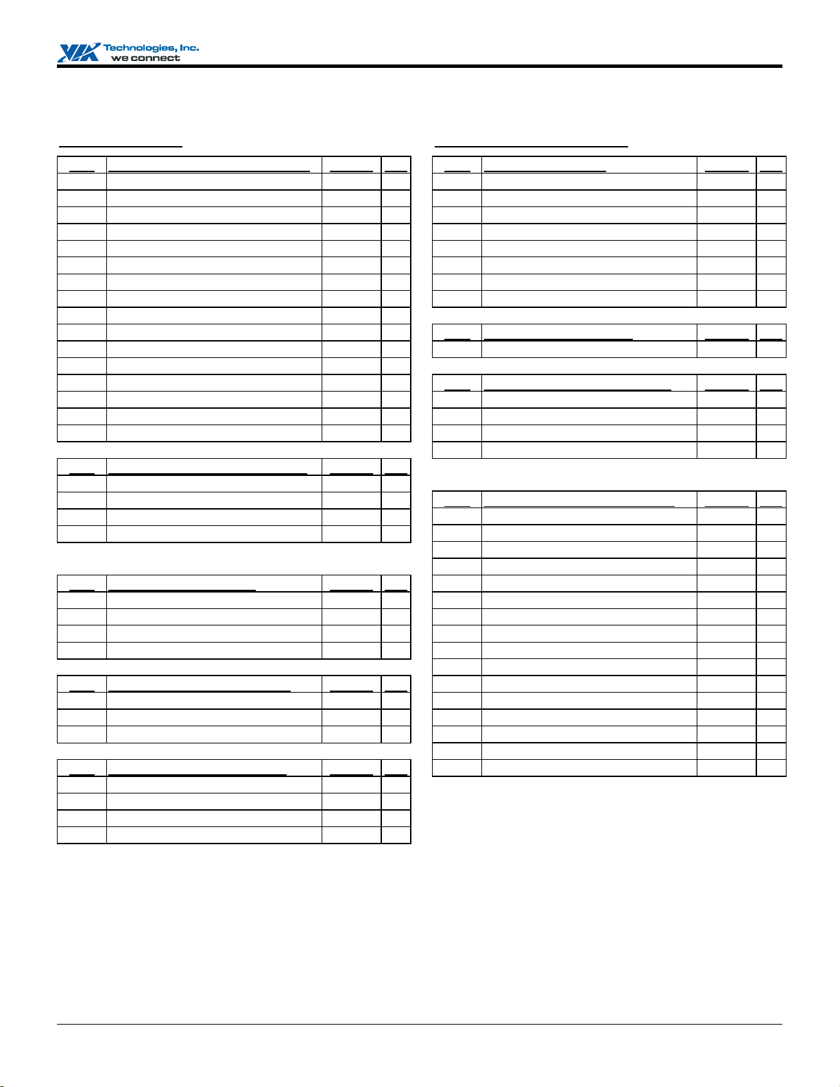
VT8235M Version CD V-Link South Bridge
Table 6. Registers
Legacy I/O Registers
Master DMA Controller Registers Default Acc
Port
00 Channel 0 Base & Current Address RW
01 Channel 0 Base & Current Count RW
02 Channel 1 Base & Current Address RW
03 Channel 1 Base & Current Count RW
04 Channel 2 Base & Current Address RW
05 Channel 2 Base & Current Count RW
06 Channel 3 Base & Current Address RW
07 Channel 3 Base & Current Count RW
08 Status / Command RW
09 Write Request
0A Write Single Mask
0B Write Mode
0C Clear Byte Pointer FF
0D Master Clear
0E Clear Mask
0F Read / Write Mask RW
Port
Master Interrupt Controller Regs Default Acc
20 Master Interrupt Control — *
21 Master Interrupt Mask — *
20 Master Interrupt Control Shadow —
21 Master Interrupt Mask Shadow —
* RW if shadow registers are disabled
Port
Timer/Counter Registers Default Acc
40 Timer / Counter 0 Count RW
41 Timer / Counter 1 Count RW
42 Timer / Counter 2 Count RW
43 Timer / Counter Control
Port
Keyboard Controller Registers Default Acc
60 Keyboard Controller Data RW
61 Misc Functions & Speaker Control RW
64 Keyboard Ctrlr Command / Status RW
Port
CMOS / RTC / NMI Registers Default Acc
70 CMOS Memory Address & NMI Disa
71 CMOS Memory Data (128 bytes) RW
74 CMOS Memory Address
75 CMOS Memory Data (256 bytes) RW
NMI Disable is port 70h (CMOS Memory Address) bit-7.
RTC control occurs via specific CMOS data locations (0-Dh).
Ports 74-75 may be used to access CMOS if the internal RTC
is disabled.
WO
WO
WO
WO
WO
WO
RW
RW
WO
WO
RW
Legacy I/O Registers (continued)
DMA Page Registers Default Acc
Port
87 DMA Page – DMA Channel 0 RW
83 DMA Page – DMA Channel 1 RW
81 DMA Page – DMA Channel 2 RW
82 DMA Page – DMA Channel 3 RW
8F DMA Page – DMA Channel 4 RW
8B DMA Page – DMA Channel 5 RW
89 DMA Page – DMA Channel 6 RW
8A DMA Page – DMA Channel 7 RW
Port
System Control Registers Default Acc
92 System Control RW
Port
Slave Interrupt Controller Regs Default Acc
A0 Slave Interrupt Control — *
A1 Slave Interrupt Mask — *
A0 Slave Interrupt Control Shadow —
A1 Slave Interrupt Mask Shadow —
* RW accessible if shadow registers are disabled
Port
Slave DMA Controller Registers Default Acc
C0 Channel 0 Base & Current Address RW
C2 Channel 0 Base & Current Count RW
C4 Channel 1 Base & Current Address RW
C6 Channel 1 Base & Current Count RW
C8 Channel 2 Base & Current Address RW
CA Channel 2 Base & Current Count RW
CC Channel 3 Base & Current Address RW
CE Channel 3 Base & Current Count RW
D0 Status / Command RW
D2 Write Request
D4 Write Single Mask
D6 Write Mode
D8 Clear Byte Pointer FF
DA Master Clear
DC Clear Mask
DE Read / Write Mask RW
WO
WO
WO
WO
WO
WO
RW
RW
Revision 2.03, March 16, 2005 -23- Register Overview
Page 31

VT8235M Version CD V-Link South Bridge
—
—
Keyyboard / Mouse Wakeup Registers (I/O Space)
KB / Mouse Wakeup Registers Default Acc
Port
002E Keyboard / Mouse Wakeup Index † 00 RW
002F Keyboard / Mouse Wakeup Data † 00 RW
† Keyboard / Mouse Wakeup registers (index values E0-EF
defined below) are accessible if Function 0 PCI
Configuration register Rx51[1] = 1.
Keyboard / Mouse Wakeup Registers (Indexed via Port
2E/2F)
Offset
Reserved Default Acc
00-DF -reserved-
Offset
KB / Mouse Wakeup (Rx51[1]=1) Default Acc
E0 Keyboard / Mouse Wakeup Enable
E1 Keyboard Wakeup Scan Code Set 0
E2 Keyboard Wakeup Scan Code Set 1 00
E3 Keyboard Wakeup Scan Code Set 2 00
E4 Keyboard Wakeup Scan Code Set 3 00
E5 Keyboard Wakeup Scan Code Set 4 00
E6 Keyboard Wakeup Scan Code Set 5 00
E7 Keyboard Wakeup Scan Code Set 6 00
E8 Keyboard Wakeup Scan Code Set 7 00
E9 Mouse Wakeup Scan Code Set 1
EA Mouse Wakeup Scan Code Set 2 00
EB Mouse Wakeup Scan Code Mask 00
EC-EF -reserved-
Game Port Registers (I/O Space)
Offset
Game Port (200-20F typical) Default Acc
0 -reserved- 00 —
1 Game Port Status
1 Start One-Shot
2-F -reserved- 00 —
08 RW
F0 RW
09 RW
RO
RW
RW
RW
RW
RW
RW
RW
RW
RW
RO
RO
WO
Memory Mapped Registers – IOAPIC
Address
FEC00000 APIC Register Index 00 RW
FEC00001-0F -reserved- 00 —
FEC00010-13 APIC Register Data 0000 0000 RW
FEC00014-1F -reserved- 00 —
FEC00020 APIC IRQ Pin Assertion xx
FEC00021-3F -reserved- 00 —
FEC00040 APIC EOI xx
FEC00041-FF -reserved- 00 —
Offset
0 APIC ID 0000 0000 RW
1 APIC Version 0017 8003
2 APIC Arbitration 0000 0000
3 Boot Configuration 0000 0000 RW
4-F -reserved- 0000 0000 —
11-10 I/O Redirection– AIRQ0 xxx1xxxx xxxxxxxx RW
13-12 I/O Redirection– AIRQ1 xxx1xxxx xxxxxxxx RW
15-14 I/O Redirection– AIRQ2 xxx1xxxx xxxxxxxx RW
17-16 I/O Redirection– AIRQ3 xxx1xxxx xxxxxxxx RW
19-18 I/O Redirection– AIRQ4 xxx1xxxx xxxxxxxx RW
1B-1A I/O Redirection– AIRQ5 xxx1xxxx xxxxxxxx RW
1D-1C I/O Redirection– AIRQ6 xxx1xxxx xxxxxxxx RW
1F-1E I/O Redirection– AIRQ7 xxx1xxxx xxxxxxxx RW
21-20 I/O Redirection– AIRQ8 xxx1xxxx xxxxxxxx RW
23-20 I/O Redirection– AIRQ9 xxx1xxxx xxxxxxxx RW
25-24 I/O Redirection– AIRQ10 xxx1xxxx xxxxxxxx RW
27-26 I/O Redirection– AIRQ11 xxx1xxxx xxxxxxxx RW
29-28 I/O Redirection– AIRQ12 xxx1xxxx xxxxxxxx RW
2B-2A I/O Redirection– AIRQ13 xxx1xxxx xxxxxxxx RW
2D-2C I/O Redirection– AIRQ14 xxx1xxxx xxxxxxxx RW
2F-2E I/O Redirection– AIRQ15 xxx1xxxx xxxxxxxx RW
31-30 I/O Redirection– AIRQ16 xxx1xxxx xxxxxxxx RW
33-32 I/O Redirection– AIRQ17 xxx1xxxx xxxxxxxx RW
35-34 I/O Redirection– AIRQ18 xxx1xxxx xxxxxxxx RW
37-36 I/O Redirection– AIRQ19 xxx1xxxx xxxxxxxx RW
39-38 I/O Redirection– AIRQ20 xxx1xxxx xxxxxxxx RW
3B-3A I/O Redirection– AIRQ21 xxx1xxxx xxxxxxxx RW
3D-3C I/O Redirection– AIRQ22 xxx1xxxx xxxxxxxx RW
3F-3E I/O Redirection– AIRQ23 xxx1xxxx xxxxxxxx RW
40-4F -reserved- 0000 0000 —
Note: The “I/O Redirection” registers are 64-bit registers, so
each uses two consecutive index locations, with the lower 32
bits at the even index and the upper 32 bits at the odd index.
APIC Index / Data Default Acc
WO
WO
APIC Registers Default Acc
RO
RO
Revision 2.03, March 16, 2005 -24- Register Overview
Page 32

VT8235M Version CD V-Link South Bridge
Device 16 Function 0 Registers – USB 1.1 UHCI Ports 0-1
Configuration Space USB Header Registers
Configuration Space Header Default Acc
Offset
1-0 Vendor ID
3-2 Device ID
5-4 Command 0000
7-6 Status
8 Revision ID
9 Programming Interface 00 RO
A Sub Class Code
B Base Class Code
C -reserved- 00 —
D Latency Timer
E-1F -reserved- 00 —
23-20 USB I/O Registers Base Port Address
24-2B -reserved- 00 —
2D-2C Sub Vendor ID
2F-2E Sub Device ID
30-33 -reserved- 00 —
34 Power Management Capabilities
35-3B -reserved- 00 —
3C Interrupt Line 00
3D Interrupt Pin
3E-3F -reserved- 00 —
† RW if Rx42[4] = 1.
1106
3038
0210 WC
nn
03
0C
16 RW
00000301 RW
1106
3038
80
01
RO
RO
RW
RO
RO
RO
RO†
RO†
RO
RW
RO
Configuration Space USB-Specific Registers
Offset
4B-5F -reserved- 00 —
85-BF -reserved- 00 —
C1-C0 USB Legacy Support
C2-FF -reserved- 00 —
Memory Mapped I/O Registers – USB Controller
Offset
USB Control Default Acc
40 USB Miscellaneous Control 1
41 USB Miscellaneous Control 2
42 USB Miscellaneous Control 3
43 USB Miscellaneous Control 4 00 RW
44-47 -reserved- (test, do not program) 00
48 USB Miscellaneous Control 5 00 RW
49 USB Miscellaneous Control 6 00 RW
4A USB Miscellaneous Control 7 00 RW
60 USB Serial Bus Release Number
61-7F -reserved- 00 —
83-80 PM Capability
84 PM Capability Status 00 RW
USB I/O Registers Default Acc
1-0 USB Command 0000 RW
3-2 USB Status 0000
5-4 USB Interrupt Enable 0000 RW
7-6 Frame Number 0000 RW
B-8 Frame List Base Address 00000000 RW
C Start Of Frame Modify
11-10 Port 0 Status / Control
13-12 Port 1 Status / Control
14-1F -reserved- 00 —
40
10
03
10 RO
FFC20001 RO
2000
40
0080 WC
0080 WC
RW
RW
RW
—
RW
WC
RW
Revision 2.03, March 16, 2005 -25- Register Overview
Page 33

VT8235M Version CD V-Link South Bridge
Device 16 Function 1 Registers – USB 1.1 UHCI Ports 2-3
Configuration Space USB Header Registers
Configuration Space Header Default Acc
Offset
1-0 Vendor ID
3-2 Device ID
5-4 Command 0000
7-6 Status
8 Revision ID
9 Programming Interface 00 RO
A Sub Class Code
B Base Class Code
C -reserved- 00 —
D Latency Timer
E-1F -reserved- 00 —
23-20 USB I/O Registers Base Port Address
24-2B -reserved- 00 —
2D-2C Sub Vendor ID
2F-2E Sub Device ID
30-33 -reserved- 00 —
34 Power Management Capabilities
35-3B -reserved- 00 —
3C Interrupt Line 00
3D Interrupt Pin
3E-3F -reserved- 00 —
† RW if Rx42[4] = 1.
1106
3038
0210 WC
nn
03
0C
16 RW
00000301 RW
1106
3038
80
02
RO
RO
RW
RO
RO
RO
RO†
RO†
RO
RW
RO
Configuration Space USB-Specific Registers
Offset
4B-5F -reserved- 00 —
85-BF -reserved- 00 —
C1-C0 USB Legacy Support
C2-FF -reserved- 00 —
Memory Mapped I/O Registers – USB Controller
Offset
USB Control Default Acc
40 USB Miscellaneous Control 1
41 USB Miscellaneous Control 2
42 USB Miscellaneous Control 3
43 USB Miscellaneous Control 4 00 RW
44-47 -reserved- (test, do not program) 00
48 USB Miscellaneous Control 5 00 RW
49 USB Miscellaneous Control 6 00 RW
4A USB Miscellaneous Control 7 00 RW
60 USB Serial Bus Release Number
61-7F -reserved- 00 —
83-80 PM Capability
84 PM Capability Status 00 RW
USB I/O Registers Default Acc
1-0 USB Command 0000 RW
3-2 USB Status 0000
5-4 USB Interrupt Enable 0000 RW
7-6 Frame Number 0000 RW
B-8 Frame List Base Address 00000000 RW
C Start Of Frame Modify
11-10 Port 0 Status / Control
13-12 Port 1 Status / Control
14-1F -reserved- 00 —
40
10
03
10 RO
FFC20001 RO
2000
40
0080 WC
0080 WC
RW
RW
RW
—
RW
WC
RW
Revision 2.03, March 16, 2005 -26- Register Overview
Page 34

VT8235M Version CD V-Link South Bridge
Device 16 Function 2 Registers – USB 1.1 UHCI Ports 4-5
Configuration Space USB Header Registers
Configuration Space Header Default Acc
Offset
1-0 Vendor ID
3-2 Device ID
5-4 Command 0000
7-6 Status
8 Revision ID
9 Programming Interface 00 RO
A Sub Class Code
B Base Class Code
C -reserved- 00 —
D Latency Timer
E-1F -reserved- 00 —
23-20 USB I/O Registers Base Port Address
24-2B -reserved- 00 —
2D-2C Sub Vendor ID
2F-2E Sub Device ID
30-33 -reserved- 00 —
34 Power Management Capabilities
35-3B -reserved- 00 —
3C Interrupt Line 00
3D Interrupt Pin
3E-3F -reserved- 00 —
† RW if Rx42[4] = 1.
1106
3038
0210 WC
nn
03
0C
16 RW
00000301 RW
1106
3038
80
03
RO
RO
RW
RO
RO
RO
RO†
RO†
RO
RW
RO
Configuration Space USB-Specific Registers
Offset
4B-5F -reserved- 00 —
85-BF -reserved- 00 —
C1-C0 USB Legacy Support
C2-FF -reserved- 00 —
Memory Mapped I/O Registers – USB Controller
Offset
USB Control Default Acc
40 USB Miscellaneous Control 1
41 USB Miscellaneous Control 2
42 USB Miscellaneous Control 3
43 USB Miscellaneous Control 4 00 RW
44-47 -reserved- (test, do not program) 00
48 USB Miscellaneous Control 5 00 RW
49 USB Miscellaneous Control 6 00 RW
4A USB Miscellaneous Control 7 00 RW
60 USB Serial Bus Release Number
61-7F -reserved- 00 —
83-80 PM Capability
84 PM Capability Status 00 RW
USB I/O Registers Default Acc
1-0 USB Command 0000 RW
3-2 USB Status 0000
5-4 USB Interrupt Enable 0000 RW
7-6 Frame Number 0000 RW
B-8 Frame List Base Address 00000000 RW
C Start Of Frame Modify
11-10 Port 0 Status / Control
13-12 Port 1 Status / Control
14-1F -reserved- 00 —
40
10
03
10 RO
FFC20001 RO
2000
40
0080 WC
0080 WC
RW
RW
RW
—
RW
WC
RW
Revision 2.03, March 16, 2005 -27- Register Overview
Page 35

VT8235M Version CD V-Link South Bridge
Device 16 Function 3 Registers – USB 2.0 EHCI Ports 0-5
Configuration Space USB Header Registers
Configuration Space Header Default Acc
Offset
1-0 Vendor ID
3-2 Device ID
5-4 Command 0000
7-6 Status
8 Revision ID
9 Programming Interface
A Sub Class Code
B Base Class Code
C Cache Line Size 00
D Latency Timer
1106
3104
0210 WC
nn
20
03
0C
16 RW
RO
RO
RW
RO
RO
RO
RO
RW
E-F -reserved- 00 —
13-10 EHCI Mem Mapped I/O Base Addr 0000 0000
RW
14-2B -reserved- 00 —
2D-2C Sub Vendor ID
2F-2E Sub Device ID
1106
3104
RO†
RO†
30-33 -reserved- 00 —
34 Power Management Capabilities
80
RO
35-3B -reserved- 00 —
3C Interrupt Line 00
3D Interrupt Pin
04
RW
RO
3E-3F -reserved- 00 —
† RW if Rx42[4] = 1.
Memory Mapped I/O Registers – USB EHCI
Offset
EHCI Capabilities Default Acc
00 Capability Register Length 00 RW
01 -reserved- 00 —
03-02 Interface Version Number
07-04 Structure Parameters
0B-08 Capability Parameters
0100
0000 3206
0000 6872
RO†
RO†
RO†
0C-0F -reserved- 00 —
† RW if Rx42[4] = 1.
Offset
Host Controller Operation Default Acc
13-10 USB Command 0000 0000 RW
17-14 USB Status 0000 0000 RW
1B-18 USB Interrupt Enable 0000 0000 RW
1F-1C USB Frame Index 0000 0000 RW
23-20 4G Segment Selector 0000 0000 RW
27-24 Frame List Base Address 0000 0000 RW
2B-28 Next Asynchronous List Address 0000 0000 RW
2C-4F -reserved- 00 —
53-50 Configured Flag Register 0000 0000 RW
57-54 Port 1 Status / Control 0000 0000 RW
5B-58 Port 2 Status / Control 0000 0000 RW
5C-FF -reserved- 00 —
Configuration Space USB-Specific Registers
USB Control Default Acc
Offset
40 USB Miscellaneous Control 1 00 RW
41-47 -reserved- (Do Not Program) 00 —
48 USB Miscellaneous Control 5
49 USB Miscellaneous Control 6
A0
20
RW
RW
4A-4B -reserved- (Do Not Program) 00 —
4C-4F -reserved- 00 —
50-57 -reserved- (test, do not program) 00
—
58-5D -reserved- (Do Not Program) 00 —
5E-5F -reserved- 00 —
60 USB Serial Bus Release Number
61 Frame Length Adjust
63-62 Port Wake Capability
20 RO
20
0001
RW
RW
64-67 -reserved- 00 —
6B-68 Legacy Support Extended Capability
0000 0001
RW
6F-6C Legacy Support Control / Status 0000 0000 RW
70-7F -reserved- 00 —
83-80 PM Capability
FFC20001 RO
84 PM Capability Status 00 RW
85-FF -reserved- 00 —
Revision 2.03, March 16, 2005 -28- Register Overview
Page 36

VT8235M Version CD V-Link South Bridge
Device 17 Function 0 Registers – Bus Control & Power
Management
Configuration Space Bus Control & PM Header Registers
Configuration Space Header Default Acc
Offset
1-0 Vendor ID
3-2 Device ID
5-4 Command
7-6 Status
8 Revision ID
9 Programming Interface 00 RO
A Sub Class Code
B Base Class Code
C -reserved- (cache line size) 00 —
D -reserved- (latency timer) 00 —
E Header Type
F Built In Self Test (BIST) 00 RO
10-27 -reserved- (base address registers) 00 —
28-2B -reserved- (unassigned) 00 —
2D-2C Sub Vendor ID 00 RO
2F-2E Sub Device ID 00 RO
30-33 -reserved- (expan. ROM base addr) 00 —
34-3B -reserved- (unassigned) 00 —
3C -reserved- (interrupt line) 00 —
3D -reserved- (interrupt pin) 00 —
3E -reserved- (min gnt) 00 —
3F -reserved- (max lat) 00 —
Configuration Space PCI-to-ISA Bridge-Specific Registers
ISA Bus Control Default Acc
Offset
40 ISA Bus Control 00 RW
41 BIOS ROM Decode Control 00 RW
42 Line Buffer Control 00 RW
43 Delay Transaction Control 00 RW
44-47 -reserved- 00 —
48 Read Pass Write Control 00 RW
49 CCA Control 00 RW
4A-4B -reserved- 00 —
Offset
Miscellaneous Control Default Acc
4C IDE Interrupt Routing 00 RW
4D -reserved- 00 —
4E Internal RTC Test Mode 00 RW
4F PCI Bus & CPU Interface Control 00 RW
1106
3177
0087 RW
0200 WC
nn
01
06
80
RO
RO
RO
RO
RO
RO
Offset
Offset
Offset
Offset
Offset
5D-5C PCS0# I/O Port Address 0000 RW
5F-5E PCS1# I/O Port Address 0000 RW
68-6B -reserved- 00 —
Offset
7D-7F -reserved- 00 —
Function Control Default Acc
50 Function Control 1
51 Function Control 2
Serial IRQ, LPC & PC/PCI Control Default Acc
52 Serial IRQ & LPC Control 00 RW
53 PC/PCI DMA Control 00 RW
Plug and Play Control Default Acc
54 PCI Interrupt Polarity 00 RW
55 PnP Routing for PCI INTA 00 RW
56 PnP Routing for PCI INTB-C 00 RW
57 PnP Routing for PCI INTD 00 RW
GPIO and Miscellaneous Control Default Acc
58 Miscellaneous Control 0
59 Miscellaneous Control 1 00 RW
5A DMA Bandwidth Control 00 RW
5B Miscellaneous Control 2 00 RW
Programmable Chip Select Control Default Acc
61-60 PCS2# I/O Port Address 0000 RW
63-62 PCS3# I/O Port Address 0000 RW
64 PCS[1-0]# I/O Port Address Mask 00 RW
65 PCS[3-2]# I/O Port Address Mask 00 RW
66 Programmable Chip Select Control 00 RW
67 Output Control
Miscellaneous Default Acc
6C ISA Positive Decoding Control 1 00 RW
6D ISA Positive Decoding Control 2 00 RW
6E ISA Positive Decoding Control 3 00 RW
6F ISA Positive Decoding Control 4 00 RW
71-70 Sub Vendor ID Backdoor 00 RW
73-72 Sub Device ID Backdoor 00 RW
70-78 -reserved- 00 —
79 PnP IRQ/DRQ Test (do not prog) 00 RW
7A IDE / USB Test (do not program) 00 RW
7B PLL Test (do not program) 00 RW
7C I/O Pad Control 00 RW
08
0D
40
04
RW
RW
RW
RW
Revision 2.03, March 16, 2005 -29- Register Overview
Page 37

VT8235M Version CD V-Link South Bridge
Configuration Space Power Management Registers
Power Management Default Acc
Offset
80 General Configuration 0 00 RW
81 General Configuration 1
82 ACPI Interrupt Select 00 RW
83 -reserved- 00
85-84 Primary Interrupt Channel 0000 RW
87-86 Secondary Interrupt Channel 0000 RW
8B-88 Power Mgmt I/O Base (256 Bytes)
8C Host Bus Power Mgmt Control 00 RW
8D Throttle / Clock Stop Control 00 RW
8E-8F -reserved- 00
93-90 GP Timer Control 0000 0000 RW
94 Power Well Control 00 RW
95 Miscellaneous Control 00 RW
96 Power On / Reset Control 00 RW
97 -reserved- 00
98 GP2 / GP3 Timer Control 00 RW
99 GP2 Timer 00 RW
9A GP3 Timer 00 RW
9B-A0 -reserved- 00
A1 Write value for Offset 9 (Prog Intfc) 00
A2 Write value for Offset A (Sub Class) 00
A3 Write value for Offset B (Base Class) 00
A4-BF -reserved- 00
C3-C0 Power Management Capability
C7-C4 Power Management Capability CSR
C8-CF -reserved- 00
04
0000 0001
0002 0001 RO
0000 0000
RW
RW
WO
WO
WO
RW
—
—
—
—
—
—
Configuration Space SMBus Registers
Offset
D1-D0 SMBus I/O Base (16 Bytes)
D7-DF -reserved- 00
Configuration Space General Purpose I/O Registers
Offset
E2-E3 -reserved- 00
Configuration Space Watchdog Timer Registers
Offset
EB-E8 Watchdog Timer Memory Base 00 RW
ED-FF -reserved- 00
System Management Bus Default Acc
0001
D2 SMBus Host Configuration 00 RW
D3 SMBus Host Slave Command 00 RW
D4 SMBus Slave Address Shadow Port 1 00 RW
D5 SMBus Slave Address Shadow Port 2 00 RW
D6 SMBus Revision ID
General Purpose I/O Default Acc
E0 GPI Inversion Control 00 RW
E1 GPI SCI / SMI Select 00 RW
E4 GPO Pin Select 00 RW
E5 GPIO I/O Select 1 00 RW
E6 GPIO I/O Select 2 00 RW
E7 GPO Output Type 00 RW
Watchdog Timer Default Acc
EC Watchdog Timer Control 00 RW
nn RO
RW
—
—
—
Revision 2.03, March 16, 2005 -30- Register Overview
Page 38

VT8235M Version CD V-Link South Bridge
I/O Space Power Management Registers
Basic Control / Status Registers Default Acc
Offset
1-0 Power Management Status 0000
WC
3-2 Power Management Enable 0000 RW
5-4 Power Management Control 0000 RW
6-7 -reserved- 00
—
B-8 Power Management Timer 0000 0000 RW
C-F -reserved- 00
—
Offset
Processor Registers Default Acc
13-10 Processor and PCI Bus Control 0000 0000 RW
14 Processor LVL2 00
15 Processor LVL3 00
16-1F -reserved- 00
RO
RO
—
Offset
General Purpose Registers Default Acc
21-20 General Purpose Status 0000
WC
23-22 General Purpose SCI Enable 0000 RW
25-24 General Purpose SMI Enable 0000 RW
26-27 -reserved- 00
—
Offset
Generic Registers Default Acc
29-28 Global Status 0000
WC
2B-2A Global Enable 0000 RW
2D-2C Global Control
0010
2E -reserved- 00
RW
—
2F SMI Command 00 RW
33-30 Primary Activity Detect Status 0000 0000
WC
37-34 Primary Activity Detect Enable 0000 0000 RW
3B-38 GP Timer Reload Enable 0000 0000 RW
3C-3F -reserved- 00
—
Offset
General Purpose I/O Registers Default Acc
40 Extended I/O Trap Status 00
41 -reserved- 00
WC
—
42 Extended I/O Trap Enable 00 RW
43-44 -reserved- 00
45 SMI / IRQ / Resume Status 00
46-47 -reserved- 00
4B-48 GPI Port Input Value
4F-4C GPO Port Output Value
50 GPI Pin Change Status
input RO
FFFFCFFF
00
51 -reserved- 00
—
RO
—
RW
RW
—
52 GPI Pin Change SCI/SMI Select 00 RW
53-57 -reserved- 00
59-58 I/O Trap PCI I/O Address 0000
5A I/O Trap PCI Command / Byte Ena 00
5B -reserved- 00
—
RO
RO
—
5C CPU Performance Control 00 RW
5D-FF -reserved- 00
—
I/O Space System Management Bus Registers
Offset
System Management Bus Default Acc
0 SMBus Host Status 00
1 SMBus Slave Status 00 RW
2 SMBus Host Control 00 RW
3 SMBus Host Command 00 RW
4 SMBus Host Address 00 RW
5 SMBus Host Data 0 00 RW
6 SMBus Host Data 1 00 RW
7 SMBus Block Data 00 RW
8 SMBus Slave Control 00 RW
9 SMBus Shadow Command 00
A-B SMBus Slave Event 0000 RW
C-D SMBus Slave Data 0000
E -reserved- 00
F SMBus GPIO Slave Address 00 RW
System Management Bus Command Codes
System Management Bus Default Acc
Code
00 SMBus GPIO Slave Input Data
— RO
01 SMBus GPIO Slave Output Data 00 RW
02 SMBus GPIO Slave Polarity Inversion
03 SMBus GPIO Slave I/O Configuration
F0
FF
WC
RO
RO
—
RW
RW
Revision 2.03, March 16, 2005 -31- Register Overview
Page 39

VT8235M Version CD V-Link South Bridge
Device 17 Function 1 Registers – IDE Controller
Configuration Space IDE Header Registers
Configuration Space Header Default Acc
Offset
1-0 Vendor ID
3-2 Device ID
5-4 Command
7-6 Status
8 Revision ID
9 Programming Interface
A Sub Class Code
B Base Class Code
C-F -reserved- 00 —
13-10 Base Address – Pri Data / Command
17-14 Base Address – Pri Control / Status
1B-18 Base Address – Sec Data / Command
1F-1C Base Address – Sec Control / Status
23-20 Base Address – Bus Master Control
24-2B -reserved- (unassigned) 00 —
2D-2C Sub Vendor ID 0000 RO
2F-2E Sub Device ID 0000 RO
30-33 -reserved- (expan ROM base addr) 00 —
34 Capability Pointer
35-3B -reserved- (unassigned) 00 —
3C Interrupt Line
3D Interrupt Pin
3E Minimum Grant 00 RO
3F Maximum Latency 00 RO
Configuration Space IDE-Specific Registers
Configuration Space IDE Registers Default Acc
Offset
40 IDE Chip Enable 00 RW
41 IDE Configuration I 00 RW
42 IDE Configuration II 00 RW
43 IDE FIFO Configuration
44 IDE Miscellaneous Control 1
45 IDE Miscellaneous Control 2
46 IDE Miscellaneous Control 3
4B-48 IDE Drive Timing Control
4C IDE Address Setup Time
4D -reserved- (do not program) 00 RW
4E Sec Non-170 Port Access Timing
4F Pri Non-1F0 Port Access Timing
1106
0571
0080
0290 RW
nn
85 RW
01
01
000001F1 RW
000003F5 RW
00000171 RW
00000375 RW
0000CC01 RW
C0
0E
01
0A
08
10
C0
A8A8A8A8
FF
B6
B6
RO
RO
RO
RO
RO
RO
RO
RO
RO
RW
RW
RW
RW
RW
RW
RW
RW
Configuration Space IDE-Specific Registers (continued)
Offset
7A-7F -reserved- 00 —
8B-88 IDE Secondary S/G Descriptor Addr 0000 0000 RW
8C-BF -reserved- 00 —
C3-C0 Power Management Capabilities
C7-C4 Power State 0000 0000 RW
C8-CF -reserved- 00 —
Offset
D3-D2 Back Door – Device ID
D5-D4 Back Door – Sub Vender ID 0000 RW
D7-D6 Back Door – Sub Device ID 0000 RW
D8-FF -reserved- 00 —
I/O Registers – IDE Controller (SFF 8038 v1.0 Compliant
Offset
Configuration Space IDE Registers Default Acc
53-50 UltraDMA Extended Timing Control
54 UltraDMA FIFO Control
55 IDE Clock Gating 00 RW
56-5F -reserved- 00 —
61-60 IDE Primary Sector Size
62-67 -reserved- 00 —
69-68 IDE Secondary Sector Size
69-6F -reserved- 00 —
70 IDE Primary Status 00 RW
71 IDE Primary Interrupt Control
72-77 -reserved- 00 —
78 IDE Secondary Status 00 RW
79 IDE Secondary Interrupt Control
83-80 IDE Primary S/G Descriptor Address 0000 0000 RW
84-87 -reserved- 00 —
IDE Back Door Registers Default Acc
D0 Back Door – Revision ID
D1 -reserved- 00 —
IDE I/O Registers Default Acc
0 Primary Channel Command 00 RW
1 -reserved- 00 —
2 Primary Channel Status 00
3 -reserved- 00 —
4-7 Primary Channel PRD Table Addr 00 RW
8 Secondary Channel Command 00 RW
9 -reserved- 00 —
A Secondary Channel Status 00
B -reserved- 00 —
C-F Secondary Channel PRD Table Addr 00 RW
07070707
04
0200
0200
01
01
0002 0001 RO
06
0571
RW
RW
RW
RW
RW
RW
RW
RW
WC
WC
Revision 2.03, March 16, 2005 -32- Register Overview
Page 40

VT8235M Version CD V-Link South Bridge
f
Device 17 Function 5 & 6 Registers – AC/MC97 Codecs
Function 5 Configuration Space AC97 Header Registers
fset Configuration Space Header Default Acc
O
1-0 Vendor ID
3-2 Device ID
5-4 Command 0000
7-6 Status
8 Revision ID
9 Programming Interface 00 RO
A Sub Class Code
B Base Class Code
C-F -reserved- 00 —
13-10 Base Address 0 - SGD Control/Status
17-14 Base Address 1 (reserved) 0000 0000 —
1B-18 Base Address 2 (reserved) 0000 0000 —
1F-1C Base Address 3 (reserved) 0000 0000 —
23-20 Base Address 4 (reserved) 0000 0000 —
27-24 Base Address 5 (reserved) 0000 0000 —
28-29 -reserved- 00 —
2F-2C Subsystem ID / SubVendor ID 0000 0000
33-30 Expansion ROM (reserved) 0000 0000 —
34 Capture Pointer
35-3B -reserved- 00 —
3C Interrupt Line 00
3D Interrupt Pin
3E Minimum Grant 00 RO
3F Maximum Latency 00 RO
1106
3059
0210
50
01
04
0000 0001 RW
C0 RW
03
RO
RO
RW
RO
RO
RO
RO
RW
RW
RO
Function 6 Configuration Space MC97 Header Registers
Offset
1B-18 Base Address 2 (reserved) 0000 0000 —
1F-1C Base Address 3 (reserved) 0000 0000 —
2F-2C Subsystem ID / SubVendor ID 0000 0000
35-3B -reserved- 00 —
Configuration Space Header Default Acc
1-0 Vendor ID
3-2 Device ID
5-4 Command 0000
7-6 Status
8 Revision ID
9 Programming Interface 00 RO
A Sub Class Code
B Base Class Code
C-F -reserved- 00 —
13-10 Base Address 0 - SGD Control/Status
17-14 Base Address 1 (reserved) 0000 0000 —
23-20 Base Address 4 (reserved) 0000 0000 —
27-24 Base Address 5 (reserved) 0000 0000 —
28-29 -reserved- 00 —
33-30 Expansion ROM (reserved) 0000 0000 —
34 Capture Pointer
3C Interrupt Line 00
3D Interrupt Pin
3E Minimum Grant 00 RO
3F Maximum Latency 00 RO
1106
3068
0200
70
80
07
0000 0001 RW
D0 RW
03
RO
RO
RW
RO
RO
RO
RO
RW
RW
RO
Configuration Space Audio Codec-Specific Registers
Audio Codec Link Control Default Acc
Offset
40 AC-Link Interface Status 00
41 AC-Link Interface Control 00 RW
42 Function Enable 00 RW
43 -reserved- 00 —
44 MC97 Interface Control 00
45-47 -reserved- 00 —
4B-48 Test Mode (reserved) 00 —
4C-BF -reserved- 00 —
C3-C0 Power Management Capability
C7-C4 Power State 0000 0000 RW
C8-FF -reserved- 00 —
0002 0001 RO
RO
RO
Configuration Space Modem Codec-Specific Registers
Offset
4B-48 Test Mode (reserved) 00 —
4C-CF -reserved- 00 —
D3-D0 Power Management Capability
D7-D4 Power State 0000 0000 RW
D8-FF -reserved- 00 —
Modem Codec Link Control Default Acc
40 AC-Link Interface Status 00
41 AC-Link Interface Control 00 RW
42 Function Enable 00
43 -reserved- 00 —
44 MC97 Interface Control 00 RW
45-47 -reserved- 00 —
0002 0001 RO
RO
RO
Revision 2.03, March 16, 2005 -33- Register Overview
Page 41

VT8235M Version CD V-Link South Bridge
Function 5 I/O Base 0 Registers – AC97 Audio S/G DMA
AC97 SGD I/O Registers Default Acc
Offset
x0 SGD Channel x Status 00
WC
x1 SGD Channel x Control 00 RW
x2 SGD Channel x Left Volume
x3 SGD Channel x Right Volume
x7-x4 SGD Channel x Table Pointer Base
3F
3F
0000 0000 WR
SGD Channel x Current Address
xB-x8 Stop Index / Data Type / Sample Rate
FF0F FFFF
xF-xC SGD Channel x Current Count 0000 0000
40 SGD 3D Channel Status 00
RW
RW
RD
RW
RO
WC
41 SGD 3D Channel Control 00 RW
42 SGD 3D Channel Format 00 RW
43 SGD 3D Channel Scratch 00 RW
47-44 SGD 3D Channel Table Pointer Base
SGD 3D Channel Current Address
4B-48 SGD 3D Channel Slot Select
4F-4C SGD 3D Channel Current Count 0000 0000
0000 0000 WR
RD
FF00 0000
RW
RO
50-5F -reserved- 00 —
60 SGD Write Channel 0 Status 00
WC
61 SGD Write Channel 0 Control 00 RW
62 SGD Write Channel 0 Format 00 RW
63 SGD Write Channel 0 Select 00 RW
67-64 SGD Write Channel 0 Table Ptr Base
SGD Write Channel 0 Current Addr
6B-68 SGD Write Channel 0 Stop Index
6F-6C SGD Write Channel 0 Current Count 0000 0000
70 SGD Write Channel 1 Status 00
0000 0000 WR
RD
FF00 0000
RW
RO
WC
71 SGD Write Channel 1 Control 00 RW
72 SGD Write Channel 1 Format 00 RW
73 SGD Write Channel 1 Select 00 RW
77-74 SGD Write Channel 1 Table Ptr Base
SGD Write Channel 1 Current Addr
7B-78 SGD Write Channel 1 Stop Index
7F-7C SGD Write Channel 1 Current Count 0000 0000
0000 0000 WR
RD
FF00 0000
RW
RO
AC97 / Audio Codec I/O Registers Default Acc
Offset
83-80 AC97 Controller Command / Status 0000 0000 RW
87-84 SGD Global IRQ Shadow 0000 0000
8B-88 Modem Codec GPI Intr Status / GPIO 0000 0000
8F-8C Modem Codec GPI Interrupt Enable 0000 0000
90-9F Shadow PCI Config Registers 40-4F n/a
RO
RO
RO
RO
A0-FF -reserved- 00 —
Function 6 I/O Base 0 Registers – MC97 Modem S/G DMA
Offset
MC97 SGD I/O Registers Default Acc
0-7 -reserved- 00 —
8-F -reserved- 00 —
10-17 -reserved- 00 —
18-1F -reserved- 00 —
20-27 -reserved- 00 —
28-2F -reserved- 00 —
30-37 -reserved- 00 —
38-3F -reserved- 00 —
40 SGD Read Channel Status 00
WC
41 SGD Read Channel Control 00 RW
42 SGD Read Channel Type 00 RW
43 -reserved- 00 —
47-44 SGD Read Chan Table Pointer Base
SGD Read Channel Current Address
4B-48 -reserved- (Test) 0000 0000
4F-4C SGD Read Channel Current Count 0000 0000
50 SGD Write Channel Status 00
0000 0000 WR
RD
RO
RO
WC
51 SGD Write Channel Control 00 RW
52 SGD Write Channel Type 00 RW
53 -reserved- 00 —
57-54 SGD Write Channel Table Ptr Base
SGD Write Channel Current Address
5B-58 Reserved (Test) 0000 0000
5F-5C SGD Write Channel Current Count 0000 0000
0000 0000 WR
RD
RO
RO
60-7F -reserved- 00 —
Offset AC97 / Modem Codec I/O Registers Default Acc
83-80 AC97 Controller Command / Status 0000 0000 RW
87-84 SGD Global IRQ Shadow 0000 0000
8B-88 Modem Codec GPI Intr Status / GPIO 0000 0000
RO
WC
8F-8C Modem Codec GPI Interrupt Enable 0000 0000 RW
90-9F Shadow PCI Config Registers 40-4F n/a
RO
A0-FF -reserved- 00 —
Revision 2.03, March 16, 2005 -34- Register Overview
Page 42

VT8235M Version CD V-Link South Bridge
Device 18 Function 0 Registers - LAN
Configuration Space LAN Header Registers
Configuration Space Header Default Acc
Offset
1-0 Vendor ID
3-2 Device ID
5-4 Command 0000 RO
7-6 Status
8 Revision ID
9 Programming Interface 00 RO
A Sub Class Code 00 RO
B Base Class Code 00 RO
C Cache Line Size 00
D Latency Timer 00
E Header Type 00 RO
F BIST 00 RO
13-10 I/O Base Address 0000 0000 RW
17-14 Memory Base Address 0000 0000 RW
18-27 -reserved- 00 —
2B-28 Card Bus CIS Pointer 0000 0000 RW
2C-2F -reserved- 00 —
33-30 Expansion ROM Base Address 0000 0000 RW
34 Capabilities Offset
35-3C -reserved- 00 —
3D Interrupt Pin
3E-3F -reserved- 00 —
1106
3065
0470 WC
40
40 RO
01 RO
RO
RO
RO
RW
RW
Configuration Space LAN Device Specific Registers
Offset
Power Management Default Acc
40 Capability ID
41 Next Item Pointer 00
43-42 Power Management Configuration
47-44 Power Management Control / Status 0000 0000
48-FF -reserved- 00
01 RO
RO
0002 RO
WC
—
Revision 2.03, March 16, 2005 -35- Register Overview
Page 43

VT8235M Version CD V-Link South Bridge
I/O Space LAN Registers
Offset
Power Management Default Acc
5-0 Ethernet Address RW
6 Receive Control 00 RW
7 Transmit Control
8 Command 0 00 RW
9 Command 1 00 RW
A-B -reserved- 00
C Interrupt Status 0 00 RW
D Interrupt Status 1 00 RW
E Interrupt Mask 0 00 RW
F Interrupt Mask 1 00 RW
17-10 Multicast Address RW
1B-18 Receive Address RW
1F-1C Transmit Address RW
23-20 Receive Status
27-24 Receive Data Buffer Control 0000 0000
2B-28 Receive Data Buffer Start Address
2F-2C Receive Data Buffer Branch Address
30-3F -reserved- 00
43-40 Transmit Status 0000 0000 RW
47-44 Transmit Data Buffer Control 0000 0000
4B-48 Transmit Data Buffer Start Address
4F-4C Transmit Data Buffer Branch Addr
50-6B -reserved- 00
6C PHY Address
6D MII Status
6E Buffer Control 0 00 RW
6F Buffer Control 1 00 RW
70 MII Management Port Command 00 RW
71 MII Management Port Address
73-72 MII Management Port Data 0000 RW
74 EEPROM Command / Status 00 RW
75-77 -reserved- 00
78 EEPROM Control 00 RW
08
0000 0400
01
13
81
RW
—
RW
RO
RO
RO
—
RO
RO
RO
—
RW
RW
RW
—
I/O Space LAN Registers (continued)
Offset
7C-7F -reserved- 00
87-8B -reserved- 00
8D-8C Flash Address 0000 RW
9D-9C Soft Timer 0 0000 RW
9F-9E Soft Timer 1 0000 RW
A0/A4 Wake On LAN Control Set / Clear 00 / 00 RW
A1/A5 Power Configuration Set / Clear 00 / 00 RW
A2/A6 -reserved- (do not program) 00 / 00
A3/A7 Wake On LAN Config Set / Clear 00 / 00 RW
A8-AF -reserved- 00
B3-B0 Pattern CRC 0 0000 0000 RW
B7-B4 Pattern CRC 1 0000 0000 RW
BB-B8 Pattern CRC 2 0000 0000 RW
BF-BC Pattern CRC 3 0000 0000 RW
CF-C0 Byte Mask 0 0000 0000 RW
DF-D0 Byte Mask 1 0000 0000 RW
EF-E0 Byte Mask 2 0000 0000 RW
FF-F0 Byte Mask 3 0000 0000 RW
Power Management Default Acc
79 Configuration 1 00 RW
7A Configuration 2 00 RW
7B Configuration 3 00 RW
—
80 Miscellaneous 1 00 RW
81 Miscellaneous 2 00 RW
82 -reserved- 00
83 Sticky Hardware Control 00 RW
84 MII Interrupt Status 00
85 -reserved- 00
86 MII Interrupt Mask 00 RW
8E -reserved- 00
8F Flash Write Data Output 00 RW
90 Flash Read / Write Command 00 RW
91 Flash Write Data Input 00
92 -reserved- 00
93 Flash Checksum 00 RW
95-94 Suspend Mode MII Address 0000 RW
96 Suspend Mode PHY Address 00 RW
97 -reserved- 00
99-98 Pause Timer 0000 RW
9A Pause Status 00 RW
9B -reserved- 00
—
WC
—
—
—
RO
—
—
—
—
—
Revision 2.03, March 16, 2005 -36- Register Overview
Page 44

VT8235M Version CD V-Link South Bridge
Register Descriptions
Legacy I/O Ports
This group of registers includes the DMA Controllers,
Interrupt Controllers, and Timer/Counters as well as a number
of miscellaneous ports originally implemented using discrete
logic on original PC/AT motherboards. All of the registers
listed are integrated on-chip. These registers are implemented
in a precise manner for backwards compatibility with previous
generations of PC hardware. These registers are listed for
information purposes only. Detailed descriptions of the
actions and programming of these registers are included in
numerous industry publications (duplication of that
information here is beyond the scope of this document). All
of these registers reside in I/O space.
Port 61 - Misc Functions & Speaker Control................. RW
7 SERR# Status .......................................................RO
0 SERR# has not been asserted ................ default
1 SERR# was asserted by a PCI agent
Note: This bit is set when the PCI bus SERR# signal
is asserted. Once set, this bit may be cleared
by setting bit-2 of this register. Bit-2 should
be cleared to enable recording of the next
SERR# (i.e., bit-2 must be set to 0 to enable
this bit to be set).
6 IOCHK# Status ....................................................RO
0 IOCHK# has not been asserted.............. default
1 IOCHK # was asserted by an ISA agent
Note: This bit is set when the ISA bus IOCHCK#
signal is asserted. Once set, this bit may be
cleared by setting bit-3 of this register. Bit-3
should be cleared to enable recording of the
next IOCHCK# (i.e., bit-3 must be set to 0 to
enable this bit to be set). IOCHCK# generates
NMI to the CPU if NMI is enabled.
5 Timer/Counter 2 Output .....................................RO
This bit reflects the output of Timer/Counter 2
without any synchronization.
4 Refresh Detected...................................................RO
This bit toggles on every rising edge of the ISA bus
REFRESH# signal.
3 IOCHK# Enable
0 Enable (see bit-6 above) ........................ default
1 Disable (force IOCHCK# inactive and clear
any “IOCHCK# Active” condition in bit-6)
2 SERR# Enable
0 Enable (see bit-7 above) ........................ default
1 Disable (force SERR# inactive and clear any
“SERR# Active” condition in bit-7)
1 Speaker Enable
0 Disable................................................... default
1 Enable Timer/Ctr 2 output to drive SPKR pin
0 Timer/Counter 2 Enable
0 Disable................................................... default
1 Enable Timer/Counter 2
Port 92h - System Control................................................ RW
7-2 Reserved ........................................always reads 0
1 A20 Address Line Enable
0 A20 disabled / forced 0 (real mode) ...... default
1 A20 address line enabled
0 High Speed Reset
0 Normal
1 Briefly pulse system reset to switch from
protected mode to real mode
Revision 2.03, March 16, 2005 -37- Legacy I/O Registers
Page 45

VT8235M Version CD V-Link South Bridge
Keyboard Controller I/O Registers
The keyboard controller handles the keyboard and mouse
interfaces. Two ports are used: port 60 and port 64. Reads
from port 64 return a status byte. Writes to port 64h are
command codes (see command code list following the register
descriptions). Input and output data is transferred via port 60.
A “Control” register is also available. It is accessable by
writing commands 20h / 60h to the command port (port 64h);
The control byte is written by first sending 60h to the
command port, then sending the control byte value. The
control register may be read by sending a command of 20h to
port 64h, waiting for “Output Buffer Full” status = 1, then
reading the control byte value from port 60h.
Traditional (non-integrated) keyboard controllers have an
“Input Port” and an “Output Port” that control pins dedicated
to specific functions. In the integrated version, connections
are hard wired as listed below. Outputs are “open-collector”
so to allow input on one of these pins, the output value for that
pin would be set high (non-driving) and the desired input
value read on the input port. These ports are defined as
follows:
Bit
Input Port
0 Keyboard Data In
1 Mouse Data In
Bit
Output Port
0 System Reset (1 = Execute Reset)
1 Gaste A20 (1 = A20 Enabled)
2 Mouse Data Out
3 Mouse Clock Out
6 Keyboard Clock Out
7 Keyboard Data Out
Bit
Test Port
0 Keyboard Clock In
1 Mouse Clock In
Hardwired Internal Connections
Keyboard Data Out (Open Collector) <=> Keyboard Data In
Keyboard Clock Out (Open Collector) <=> Keyboard Clk In
Mouse Data Out (Open Collector) <=> Mouse Data In
Mouse Clock Out (Open Collector) <=> Mouse Clock In
Keyboard OBF Interrupt => IRQ1
Mouse OBF Interrupt => IRQ12
Input / Output / Test Port Command Codes
C0h transfers input port data to the output buffer.
D0h copies output port values to the output buffer.
E0h transfers test input port data to the output buffer.
The above definitions are provided for reference only as actual
keyboard and mouse control is no longer performed bit-by bit
using the above ports but controlled directly by keyboard /
mouse controller internal logic. Data is sent and received
using the command codes listed on the following page.
Port 60 - Keyboard Controller Input Buffer.................. WO
Only write to port 60h if port 64h bit-1 = 0 (1=full).
Port 60 - Keyboard Controller Output Buffer................ RO
Only read from port 60h if port 64h bit-0 = 1 (0=empty).
Port 64 - Keyboard / Mouse Status .................................. RO
7 Parity Error
0 No parity error (odd parity received)..... default
1 Even parity occurred on last byte received
from keyboard / mouse
6 General Receive / Transmit Timeout
0 No error ................................................. default
1 Error
5 Mouse Output Buffer Full
0 Mouse output buffer empty ................... default
1 Mouse output buffer holds mouse data
4 Keylock Status
0 Locked
1 Free
3 Command / Data
0 Last write was data write ....................... default
1 Last write was command write
2 System Flag
0 Power-On Default.................................. default
1 Self Test Successful
1 Input Buffer Full
0 Input Buffer Empty ............................... default
1 Input Buffer Full
0 Keyboard Output Buffer Full
0 Keyboard Output Buffer Empty ............ default
1 Keyboard Output Buffer Full
KBC Control Register..........(R/W via Commands 20h/60h)
7 Reserved ........................................always reads 0
6 PC Compatibility
0 Disable scan conversion
1 Convert scan codes to PC format; convert 2-
byte break sequences to 1-byte PC-compatible
break codes............................................ default
5 Mouse Interface
0 Enable.................................................... default
1 Disable
4 Keyboard Interface
0 Enable.................................................... default
1 Disable
3 Reserved ........................................ always reads 0
2 System Flag ................................................ default=0
This bit may be read back as status register bit-2
1 Mouse Interrupts
0 Disable................................................... default
1 Enable - Generate interrupt on IRQ12 when
mouse data comes into output buffer
0 Keyboard Interrupts
0 Disable................................................... default
1 Enable - Generate interrupt on IRQ1 when
output buffer has been written.
Revision 2.03, March 16, 2005 -38- Legacy I/O Registers
Page 46

VT8235M Version CD V-Link South Bridge
Port 64 - Keyboard / Mouse Command ..........................WO
This port is used to send commands to the keyboard / mouse
controller. The command codes recognized by the VT8235M
Version CD are listed in the table below.
Table 7. Keyboard Controller Command Codes
Code Keyboard Command Code Description
20h Read Control Byte (next byte is Control Byte)
21-3Fh Read SRAM Data (next byte is Data Byte)
60h Write Control Byte (next byte is Control Byte)
61-7Fh Write SRAM Data (next byte is Data Byte)
A1h Output Keyboard Controller Version #
A4h Test if Password is installed
(always returns F1h to indicate not installed)
A7h Disable Mouse Interface
A8h Enable Mouse Interface
A9h Mouse Interface Test (puts test results in port 60h)
(value: 0=OK, 1=clk stuck low, 2=clk stuck high,
3=data stuck lo, 4=data stuck hi, FF=general error)
AAh KBC self test (returns 55h if OK, FCh if not)
ABh Keyboard Interface Test (see A9h Mouse Test)
ADh Disable Keyboard Interface
AEh Enable Keyboard Interface
AFh Return Version #
C0h Read Input Port (read input data to output buffer)
C1h Poll Input Port (read Mouse Data In
continuously to status bit 5
C8h Unblock Mouse Output (use before D1 to change
active mode)
C9h Reblock Mouse Output (protection mechanism
for D1)
CAh Read Mode (output KBC mode info to port 60
output buffer: bit-0=0 if ISA, 1 if PS/2)
D0h Read Output Port (copy output port values
to port 60)
D1h Write Output Port (data byte following is written to
keyboard output port as if it came from keyboard)
D2h Write Keyboard Output Buffer & clear status bit-5
(write following byte to keyboard)
D3h Write Mouse Output Buffer & set status bit-5 (write
following byte to mouse; put value in mouse input
buffer so it appears to have come from the mouse)
D4h Write Mouse (write following byte to mouse)
E0h Read Keyboard Clock In and Mouse Clock In
(return in bits 0-1 respectively of response byte)
Exh Set Mouse Clock Out per command bit 3
Set Mouse Data Out per command bit 2
Set Gate A20 per command bit 1
Fxh Pulse Mouse Clock Out low for 6usec per cmd bit 3
Pulse Mouse Data Out low for 6usec per cmd bit 2
Pulse Gate A20 low for 6usec per command bit 1
Pulse System Reset low for 6usec per cmd bit 0
All other codes not listed are undefined.
Revision 2.03, March 16, 2005 -39- Legacy I/O Registers
Page 47

VT8235M Version CD V-Link South Bridge
DMA Controller I/O Registers
Ports 00-0F - Master DMA Controller
Channels 0-3 of the Master DMA Controller control System
DMA Channels 0-3. There are 16 Master DMA Controller
registers:
I/O Address Bits 15-0
Register Name
0000 0000 000x 0000 Ch 0 Base / Current Address RW
0000 0000 000x 0001 Ch 0 Base / Current Count RW
0000 0000 000x 0010 Ch 1 Base / Current Address RW
0000 0000 000x 0011 Ch 1 Base / Current Count RW
0000 0000 000x 0100 Ch 2 Base / Current Address RW
0000 0000 000x 0101 Ch 2 Base / Current Count RW
0000 0000 000x 0110 Ch 3 Base / Current Address RW
0000 0000 000x 0111 Ch 3 Base / Current Count RW
0000 0000 000x 1000 Status / Command RW
0000 0000 000x 1001 Write Request WO
0000 0000 000x 1010 Write Single Mask WO
0000 0000 000x 1011 Write Mode WO
0000 0000 000x 1100 Clear Byte Pointer F/F WO
0000 0000 000x 1101 Master Clear WO
0000 0000 000x 1110 Clear Mask WO
0000 0000 000x 1111 R/W All Mask Bits RW
Ports C0-DF - Slave DMA Controller
Channels 0-3 of the Slave DMA Controller control System
DMA Channels 4-7. There are 16 Slave DMA Controller
registers:
I/O Address Bits 15-0
Register Name
0000 0000 1100 000x Ch 4 Base / Current Address RW
0000 0000 1100 001x Ch 4 Base / Current Count RW
0000 0000 1100 010x Ch 5 Base / Current Address RW
0000 0000 1100 011x Ch 5 Base / Current Count RW
0000 0000 1100 100x Ch 6 Base / Current Address RW
0000 0000 1100 101x Ch 6 Base / Current Count RW
0000 0000 1100 110x Ch 7 Base / Current Address RW
0000 0000 1100 111x Ch 7 Base / Current Count RW
0000 0000 1101 000x Status / Command RW
0000 0000 1101 001x Write Request WO
0000 0000 1101 010x Write Single Mask WO
0000 0000 1101 011x Write Mode WO
0000 0000 1101 100x Clear Byte Pointer F/F WO
0000 0000 1101 101x Master Clear WO
0000 0000 1101 110x Clear Mask WO
0000 0000 1101 111x Read/Write All Mask Bits WO
Note that not all bits of the address are decoded.
The Master and Slave DMA Controllers are compatible with
the Intel 8237 DMA Controller chip. Detailed description of
8237 DMA controller operation can be obtained from the Intel
Peripheral Components Data Book and numerous other
industry publications.
Ports 80-8F - DMA Page Registers
There are eight DMA Page Registers, one for each DMA
channel. These registers provide bits 16-23 of the 24-bit
address for each DMA channel (bits 0-15 are stored in
registers in the Master and Slave DMA Controllers). They are
located at the following I/O Port addresses:
I/O Address Bits 15-0
Register Name
0000 0000 1000 0111 Channel 0 DMA Page (M-0) .........RW
0000 0000 1000 0011 Channel 1 DMA Page (M-1) .........RW
0000 0000 1000 0001 Channel 2 DMA Page (M-2) .........RW
0000 0000 1000 0010 Channel 3 DMA Page (M-3) .........RW
0000 0000 1000 1111 Channel 4 DMA Page (S-0)...........RW
0000 0000 1000 1011 Channel 5 DMA Page (S-1)...........RW
0000 0000 1000 1001 Channel 6 DMA Page (S-2)...........RW
0000 0000 1000 1010 Channel 7 DMA Page (S-3) ..........RW
DMA Controller Shadow Registers
The DMA Controller shadow registers are enabled by setting
function 0 Rx77 bit 0. If the shadow registers are enabled,
they are read back at the indicated I/O port instead of the
standard DMA controller registers (writes are unchanged).
Port 0 –Channel 0 Base Address ...................................... RO
Port 1 –Channel 0 Byte Count.......................................... RO
Port 2 –Channel 1 Base Address ...................................... RO
Port 3 –Channel 1 Byte Count.......................................... RO
Port 4 –Channel 2 Base Address ...................................... RO
Port 5 –Channel 2 Byte Count.......................................... RO
Port 6 –Channel 3 Base Address ...................................... RO
Port 7 –Channel 3 Byte Count.......................................... RO
Port 8 –1
Port 8 –2
Port 8 –3
Port 8 –4
Port 8 –5
Port 8 –6
st
Read Channel 0-3 Command Register .......... RO
nd
Read Channel 0-3 Request Register ............. RO
rd
Read Channel 0 Mode Register..................... RO
th
Read Channel 1 Mode Register ..................... RO
th
Read Channel 2 Mode Register ..................... RO
th
Read Channel 3 Mode Register ..................... RO
Port F –Channel 0-3 Read All Mask................................ RO
Port C4 –Channel 5 Base Address ................................... RO
Port C6 –Channel 5 Byte Count....................................... RO
Port C8 –Channel 6 Base Address ................................... RO
Port CA –Channel 6 Byte Count...................................... RO
Port CC –Channel 7 Base Address .................................. RO
Port CE –Channel 7 Byte Count ...................................... RO
Port D0 –1
Port D0 –2
Port D0 –3
Port D0 –4
Port D0 –5
Port D0 –6
st
Read Channel 4-7 Command Register ....... RO
nd
Read Channel 4-7 Request Register .......... RO
rd
Read Channel 4 Mode Register.................. RO
th
Read Channel 5 Mode Register .................. RO
th
Read Channel 6 Mode Register .................. RO
th
Read Channel 7 Mode Register .................. RO
Port DE –Channel 4-7 Read All Mask............................. RO
Revision 2.03, March 16, 2005 -40- Legacy I/O Registers
Page 48

VT8235M Version CD V-Link South Bridge
Interrupt Controller I/O Registers
Ports 20-21 - Master Interrupt Controller
The Master Interrupt Controller controls system interrupt
channels 0-7. Two registers control the Master Interrupt
Controller. They are:
I/O Address Bits 15-0
Register Name
0000 0000 001x xxx0 Master Interrupt Control RW
0000 0000 001x xxx1 Master Interrupt Mask RW
Note that not all bits of the address are decoded.
The Master Interrupt Controller is compatible with the Intel
8259 Interrupt Controller chip. Detailed descriptions of 8259
Interrupt Controller operation can be obtained from the Intel
Peripheral Components Data Book and numerous other
industry publications.
Ports A0-A1 - Slave Interrupt Controller
The Slave Interrupt Controller controls system interrupt
channels 8-15. The slave system interrupt controller also
occupies two register locations:
I/O Address Bits 15-0
Register Name
0000 0000 101x xxx0 Slave Interrupt Control RW
0000 0000 101x xxx1 Slave Interrupt Mask RW
Note that not all address bits are decoded.
The Slave Interrupt Controller is compatible with the Intel
8259 Interrupt Controller chip. Detailed descriptions of 8259
Interrupt Controller operation can be obtained from the Intel
Peripheral Components Data Book and numerous other
industry publications.
Interrupt Controller Shadow Registers
The following shadow registers are enabled by setting
function 0 Rx47[4]. If the shadow registers are enabled, they
are read back at the indicated I/O port instead of the standard
interrupt controller registers (writes are unchanged).
Port 20 - Master Interrupt Control Shadow ................... RO
Port A0 - Slave Interrupt Control Shadow ..................... RO
7 Reserved ........................................always reads 0
6 OCW3 bit 2 (POLL)
5 OCW3 bit 0 (RIS)
4 OCW3 bit 5 (SMM)
3 OCW2 bit 7 (R)
2 ICW4 bit 4 (SFNM)
1 ICW4 bit 1 (AEOI)
0 ICW1 bit 3 (LTIM)
Port 21 - Master Interrupt Mask Shadow....................... RO
Port A1 - Slave Interrupt Mask Shadow ........................ RO
7-5 Reserved ........................................always reads 0
4-0 T7-T3 of Interrupt Vector Address
Timer / Counter Registers
Ports 40-43 - Timer / Counter I/O Registers
There are 4 Timer / Counter registers:
I/O Address Bits 15-0
Register Name
0000 0000 010x xx00 Timer / Counter 0 Count RW
0000 0000 010x xx01 Timer / Counter 1 Count RW
0000 0000 010x xx10 Timer / Counter 2 Count RW
0000 0000 010x xx11 Timer / Counter Cmd Mode WO
Note that not all bits of the address are decoded.
The Timer / Counters are compatible with the Intel 8254
Timer / Counter chip. Detailed descriptions of 8254 Timer /
Counter operation can be obtained from the Intel Peripheral
Components Data Book and numerous other industry
publications.
Timer / Counter Shadow Registers
The following shadow registers are enabled for readback by
setting function 0 Rx47[4]. If the shadow registers are
enabled, they are read back at the indicated I/O port instead of
the standard timer / counter registers (writes are unchanged).
Port 40 – Counter 0 Base Count Value (LSB 1
Port 41 – Counter 1 Base Count Value (LSB 1
Port 42 – Counter 2 Base Count Value (LSB 1
st
MSB 2nd)RO
st
MSB 2nd)RO
st
MSB 2nd)RO
Revision 2.03, March 16, 2005 -41- Legacy I/O Registers
Page 49

VT8235M Version CD V-Link South Bridge
CMOS / RTC I/O Registers
Port 70 - CMOS Address.................................................. RW
7 NMI Disable ........................................................ RW
0 Enable NMI Generation. NMI is asserted on
encountering SERR# on the PCI bus.
1 Disable NMI Generation ........................default
6-0 CMOS Address (lower 128 bytes) ...................... RW
Port 71 - CMOS Data........................................................RW
7-0 CMOS Data (128 bytes)
Note: Ports 70-71 may be accessed if Device 17 Function 0
Rx51 bit-3 is set to one to select the internal RTC. If
Rx51 bit-3 is set to zero, accesses to ports 70-71 will
be directed to an external RTC.
Port 74 - CMOS Address.................................................. RW
7-0 CMOS Address (256 bytes) ................................ RW
Port 75 - CMOS Data........................................................RW
7-0 CMOS Data (256 bytes)
Note: Ports 74-75 may be accessed only if Rx4E bit-3 (Port
74/75 Access Enable) is set to one to enable port
74/75 access.
Note: Ports 70-71 are compatible with PC industry-
standards and may be used to access the lower 128
bytes of the 256-byte on-chip CMOS RAM. Ports 7475 may be used to access the full on-chip extended
256-byte space in cases where the on-chip RTC is
disabled.
Note: The system Real Time Clock (RTC) is part of the
“CMOS” block. The RTC control registers are
located at specific offsets in the CMOS data area (00Dh and 7D-7Fh). Detailed descriptions of CMOS /
RTC operation and programming can be obtained
from the VIA VT82887 Data Book or numerous
other industry publications. For reference, the
definition of the RTC register locations and bits are
summarized in the following table:
Offset
00 Seconds 00-3Bh 00-59h
01 Seconds Alarm 00-3Bh 00-59h
02 Minutes 00-3Bh 00-59h
03 Minutes Alarm 00-3Bh 00-59h
04 Hours am 12hr: 01-1Ch 01-12h
pm 12hr: 81-8Ch 81-92h
24hr: 00-17h 00-23h
05 Hours Alarm am 12hr: 01-1Ch 01-12h
pm 12hr: 81-8Ch 81-92h
24hr: 00-17h 00-23h
06 Day of the Week Sun=1: 01-07h 01-07h
07 Day of the Month 01-1Fh 01-31h
08 Month 01-0Ch 01-12h
09 Year 00-63h 00-99h
0A Register A
7 UIP Update In Progress
6-4 DV2-0 Divide (010=ena osc & keep time)
3-0 RS3-0 Rate Select for Periodic Interrupt
0B Register B
7 SET Inhibit Update Transfers
6 PIE Periodic Interrupt Enable
5 AIE Alarm Interrupt Enable
4 UIE Update Ended Interrupt Enable
3 SQWE No function (read/write bit)
2 DM Data Mode (0=BCD, 1=binary)
1 24/12 Hours Byte Format (0=12, 1=24)
0 DSE Daylight Savings Enable
0C Register C
7 IRQF Interrupt Request Flag
6 PF Periodic Interrupt Flag
5 AF Alarm Interrupt Flag
4 UF Update Ended Flag
3-0 0 Unused (always read 0)
0D Register D
7 VRT Reads 1 if VBAT voltage is OK
6-0 0 Unused (always read 0)
0E-7C Software-Defined Storage Registers (111 Bytes)
Offset
7D Date Alarm 01-1Fh 01-31h
7E Month Alarm 01-0Ch 01-12h
7F Century Field 13-14h 19-20h
80-FF Software-Defined Storage Registers (128 Bytes)
Description Binary Range BCD Range
Extended Functions Binary Range BCD Range
Table 8. CMOS Register Summary
Revision 2.03, March 16, 2005 -42- Legacy I/O Registers
Page 50

VT8235M Version CD V-Link South Bridge
Keyboard / Mouse Wakeup Index / Data Registers
The Keyboard / Mouse Wakeup registers are accessed by
performing I/O operations to / from an index / data pair of
registers in system I/O space at port addresses 2Eh and 2Fh.
The registers accessed using this mechanism are used to
initialize Keyboard / Mouse Wakeup functions at index values
in the range of E0-EF.
Keyboard / Mouse Wakeup initialization is accomplished in
three steps:
1) Enter initialization mode (set Function 0 Rx51[1] = 1)
2) Initialize the chip
a) Write index to port 2Eh
b) Read / write data from / to port 2Fh
c) Repeat a and b for all desired registers
3) Exit initialization mode (set Function 0 Rx51[1] = 0)
Port 2Eh – Keyboard Wakeup Index ..............................RW
7-0 Index Value
Function 0 PCI configuration space register Rx51[1] must be
set to 1 to enable access to the configuration registers.
Port 2Fh – Keyboard Wakeup Data................................ RW
7-0 Data Value
Keyboard / Mouse Wakeup Registers
These registers are accessed via the port 2E / 2F index / data
register pair with Function 0 Rx51[1] = 1 using the indicated
index values below
Index E1 – Keyboard Wakeup Scan Code Set 0 (F0h).. RW
7-0 Keyboard Wakeup First Scan Code .........def = F0h
Index E2 – Keyboard Wakeup Scan Code Set 1 (00h) .. RW
7-0 Keyboard Wakeup Second Scan Code ..... def = 00h
Index E3 – Keyboard Wakeup Scan Code Set 2 (00h) .. RW
7-0 Keyboard Wakeup Third Scan Code .......def = 00h
Index E4 – Keyboard Wakeup Scan Code Set 3 (00h) .. RW
7-0 Keyboard Wakeup Fourth Scan Code ..... def = 00h
Index E5 – Keyboard Wakeup Scan Code Set 4 (00h) .. RW
7-0 Keyboard Wakeup Fifth Scan Code......... def = 00h
Index E6 – Keyboard Wakeup Scan Code Set 5 (00h) .. RW
7-0 Keyboard Wakeup Sixth Scan Code ........def = 00h
Index E7 – Keyboard Wakeup Scan Code Set 6 (00h) .. RW
7-0 Keyboard Wakeup Seventh Scan Code.... def = 00h
Index E8 – Keyboard Wakeup Scan Code Set 7 (00h) .. RW
7-0 Keyboard Wakeup Eighth Scan Code...... def = 00h
Index E9 –Mouse Wakeup Scan Code Set 1 (09h)......... RW
7-0 Mouse Wakeup Scan Code Set 1............... def = 09h
Index EA –Mouse Wakeup Scan Code Set 2(00h) ......... RW
7-0 Mouse Wakeup Scan Code Set 2............... def = 00h
Index EB –Mouse Wakeup Scan Code Mask (00h) ....... RW
7-0 Mouse Wakeup Scan Code Mask..............def = 00h
Index E0 – Keyboard / Mouse Wakeup Enable (08h).... RW
7-5 Reserved ........................................ always reads 0
4 Reserved (Do Not Program).................... default = 0
3 Win98 Keyboard Power Key Wake-up
0 Disable
1 Enable...................................................default
2 Password Wake-up
0 Disable ...................................................default
1 Enable
1 PS/2 Mouse Wake-up
0 Disable ...................................................default
1 Enable
0 Keyboard Wake-up
0 Disable ...................................................default
1 Enable
Revision 2.03, March 16, 2005 -43- KBC Configuration Registers
Page 51

VT8235M Version CD V-Link South Bridge
Memory Mapped I/O APIC Registers
Memory Address FEC00000 – APIC Index....................RW
7-0 APIC Index .......................................... default = 00h
8-bit pointer to APIC registers.
Memory Address FEC00013-10 – APIC Data................RW
31-0 APIC Data ............................. default = 0000 0000h
Data for the APIC register pointed to by the APIC
index
Memory Address FEC00020 – APIC IRQ Pin AssertionWO
7-5 Reserved ........................................ always reads 0
4-0 APIC IRQ Number ........................default undefined
IRQ # for this interrupt. Valid values are 0-23 only.
Memory Address FEC00040 – APIC EOI ......................WO
7-0 Redirection Entry Clear................default undefined
When a write is issued to this register, the APIC will
check this field and compare it with the vector field
for each entry in the I/O redirection table. When a
match is found, the “Remote_IRR” bit for that I/O
Redirection Entry will be cleared.
Indexed I/O APIC Registers
Offset 0 – APIC Identification (0000 0000h) .................. RW
31-28 Reserved ........................................always reads 0
27-24 APIC Identification.................................. default = 0
Software must program this value before using the
23-0 Reserved ........................................ always reads 0
Offset 1 – APIC Version (00178003) ................................ RO
31-24 Reserved ....................................always reads 00h
23-16 Maximum Redirection ...................always reads 17h
Equal to the number of APIC interrupt pins minus
15 PCI IRQ
Always reads 1 to indicate that the IRQ assertion
14-8 Reserved ........................................ always reads 0
7-0 APIC Version.................................. always reads 03h
The implementation version for this APIC is 03h.
Offset 2 – APIC Arbitration (0000 0000h) ...................... RO
31-28 Reserved ....................................always reads 00h
27-24 APIC Arbitration ID...................... always reads 00h
23-0 Reserved .................................... always reads 00h
APIC.
one. For this APIC, this value is 17h (23 decimal).
register is implemented and that PCI devices are
allowed to write to it to cause interrupts.
Offset 3 – Boot Configuration (0000 0000h)................... RW
31-1 Reserved .................................... always reads 00h
0 Interrupt Delivery Mechanism
0 APIC Serial Bus .................................... default
1 Front Side Bus Message
Revision 2.03, March 16, 2005 -44- Memory Mapped I/O APIC Registers
Page 52

VT8235M Version CD V-Link South Bridge
Offset 3F-10 – I/O Redirection Table
This table contains 24 registers, with one dedicated table entry
for each of the 24 APIC interrupt signals. Each 64-bit register
consists of two 32-bit values at consecutive index locations,
with the low 32 bits at the even index and the upper 32 bits at
the odd index. The default value for all registers is xxx1 xxxx
xxxx xxxxh.
Offset 11-10 – I/O Redirection – APIC IRQ0 .................RW
Offset 13-12 – I/O Redirection – APIC IRQ1 .................RW
Offset 15-14 – I/O Redirection – APIC IRQ2 .................RW
Offset 17-16 – I/O Redirection – APIC IRQ3 .................RW
Offset 19-18 – I/O Redirection – APIC IRQ4 .................RW
Offset 1B-1A – I/O Redirection – APIC IRQ5................RW
Offset 1D-1C – I/O Redirection – APIC IRQ6 ...............RW
Offset 1F-1E – I/O Redirection – APIC IRQ7................RW
Offset 21-20 – I/O Redirection – APIC IRQ8 .................RW
Offset 23-22 – I/O Redirection – APIC IRQ9 .................RW
Offset 25-24 – I/O Redirection – APIC IRQ10 ...............RW
Offset 27-26 – I/O Redirection – APIC IRQ11 ...............RW
Offset 29-28 – I/O Redirection – APIC IRQ12 ...............RW
Offset 2B-2A – I/O Redirection – APIC IRQ13..............RW
Offset 2D-2C – I/O Redirection – APIC IRQ14 .............RW
Offset 2F-2E – I/O Redirection – APIC IRQ15..............RW
Offset 31-30 – I/O Redirection – APIC IRQ16 ...............RW
Offset 33-32 – I/O Redirection – APIC IRQ17 ...............RW
Offset 35-34 – I/O Redirection – APIC IRQ18 ...............RW
Offset 37-36 – I/O Redirection – APIC IRQ19 ...............RW
Offset 39-38 – I/O Redirection – APIC IRQ20 ...............RW
Offset 3B-3A – I/O Redirection – APIC IRQ21..............RW
Offset 3D-3C – I/O Redirection – APIC IRQ22 .............RW
Offset 3F-3E – I/O Redirection – APIC IRQ23..............RW
Format for Each I/O Redirection Table Entry:
Physical Mode (bit-11=0)
63-60 Reserved ........................................always reads 0
59-56 APIC ID ................................ default = undefined
Logical Mode (bit-11=1)
63-56 Destination ................................ default = undefined
55-17 Reserved ........................................always reads 0
16 Interrupt Masked
0 Not masked............................................ default
1 Masked
15 Trigger Mode
0 Edge Sensitive ....................................... default
1 Level Sensitive
14 Remote IRR (Level Sensitive Interrupts Only) RO
0 EOI message with a matching interrupt vector
1 Level sensitive interrupt sent by IOAPIC
13 Interrupt Input Pin Polarity
0 Active High ........................................... default
1 Active Low
12 Delivery Status..................................................... RO
Contains the current status of the delivery of this
0 Idle (no activity)
1 Send Pending (the interrupt has been injected
11 Destination Mode
Determines the interpretation of bits 56-63.
0 Physical Mode ....................................... default
1 Logical Mode
10-8 Delivery Mode
Specifies how the APICs listed in the destination
000 Fixed .................................................... default
001 Lowest Priority
010 SMI
011 -reserved 100 NMI
101 INIT
110 -reserved 111 External INT
7-0 Interrupt Vector
Contains the interrupt vector for this interrupt.
received from a local APIC
accepted by local APIC(s)
interrupt.
but its delivery is temporarily delayed either
because the APIC bus is busy or because the
receiving APIC unit cannot currently accept
the interrupt)
field should act upon reception of this signal
Vector values range from 10h to FEh.
Revision 2.03, March 16, 2005 -45- Memory Mapped I/O APIC Registers
Page 53

VT8235M Version CD V-Link South Bridge
Configuration Space I/O
Configuration space accesses for all functions use PCI
configuration mechanism 1 (see PCI specification revision 2.2
for more details). The ports respond only to double-word
accesses. Byte or word accesses will be passed on unchanged.
Port CFB-CF8 - Configuration Address ......................... RW
31 Configuration Space Enable
0 Disabled .................................................default
1 Convert configuration data port writes to
configuration cycles on the PCI bus
30-24 Reserved ........................................ always reads 0
23-16 PCI Bus Number
Used to choose a specific PCI bus in the system
15-11 Device Number
Used to choose a specific device in the system
10-8 Function Number
Used to choose a specific function if the selected
device supports multiple functions
7-2 Register Number
Used to select a specific doubleword in the device’s
configuration space
1-0 Fixed ........................................ always reads 0
Port CFF-CFC - Configuration Data ..............................RW
There are 8 “functions” implemented in the VT8235M
Version CD (see Table 5 on page 22). The following sections
describe the registers and register bits of these functions.
Revision 2.03, March 16, 2005 -46- PCI Configuration Space I/O Registers
Page 54

VT8235M Version CD V-Link South Bridge
Device 16 Function 0 Registers - USB 1.1 UHCI Ports 0-1
This Universal Serial Bus host controller interface is fully
compatible with UHCI specification v1.1. There are two sets
of software accessible registers: PCI configuration registers
and USB I/O registers. The PCI configuration registers are
located in the Device 16 Function 0 PCI configuration space
of the VT8235M Version CD. The USB I/O registers are
defined in UHCI specification v1.1. The registers in this
function control USB ports 0-1 (see function 1 for ports 2-3
and function 2 for ports 4-5).
PCI Configuration Space Header
Offset 1-0 - Vendor ID (1106h) .........................................RO
15-0 Vendor ID ................. (1106h = VIA Technologies)
Offset 3-2 - Device ID (3038h)...........................................RO
15-0 Device ID (3038h = VT8235M-CD USB Controller)
Offset 5-4 - Command (0000h).........................................RW
15-8 Reserved ........................................ always reads 0
7 Reserved (address stepping) ........................fixed at 0
6 Reserved (parity error response)..................fixed at 0
5 Reserved (VGA palette snoop) ....................fixed at 0
4 Memory Write and Invalidate . default=0 (disabled)
3 Reserved (special cycle monitoring)............fixed at 0
2 Bus Master ............................... default=0 (disabled)
1 Memory Space........................... default=0 (disabled)
0 I/O Space ............................... default=0 (disabled)
Offset 7-6 - Status (0210h) ............................................. RWC
15 Reserved (detected parity error).......... always reads 0
14 Signalled System Error ............................. default=0
13 Received Master Abort.............................. default=0
12 Received Target Abort .............................. default=0
11 Signalled Target Abort.............................. default=0
10-9 DEVSEL# Timing
00 Fast
01 Medium......................................default (fixed)
10 Slow
11 Reserved
8-0 Reserved ...............................fixed 10h (PCI PMI)
Offset 8 - Revision ID (nnh).............................................. RO
7-0 Silicon Revision Code (0 indicates first silicon)
Offset 9 - Programming Interface (00h).......................... RO
Offset A - Sub Class Code (03h=USB Controller) .......... RO
Offset B - Base Class Code (0Ch=Serial Bus Controller)RO
Offset D - Latency Timer (16h) ....................................... RW
Offset 23-20 - USB I/O Register Base Address............... RW
31-16 Reserved ........................................ always reads 0
15-5 USB I/O Register Base Address. Port Address for
the base of the 32-byte USB I/O Register block,
corresponding to AD[15:5]
4-0 00001b
Offset 2D-2C - Sub Vendor ID (1106h).......................... RO†
Offset 2F-2E - Sub Device ID (3038h)............................ RO†
† RW if Rx42[4] = 1.
Offset 34 - Power Management Capabilities (80h) ........ RW
Offset 3C - Interrupt Line (00h)...................................... RW
7-4 Reserved ........................................always reads 0
3-0 USB Interrupt Routing
0000 Disabled................................................. default
0001 IRQ1
0010 Reserved
0011 IRQ3
0100 IRQ4
0101 IRQ5
0110 IRQ6
0111 IRQ7
1000 IRQ8
1001 IRQ9
1010 IRQ10
1011 IRQ11
1100 IRQ12
1101 IRQ13
1110 IRQ14
1111 Disabled
Offset 3D - Interrupt Pin (01h)......................................... RO
7-0 Interrupt Pin..........................default = 01h (INTA#)
Revision 2.03, March 16, 2005 -47- Device 16 Function 0 USB 1.1 UHCI Registers for Ports 0-1
Page 55

VT8235M Version CD V-Link South Bridge
USB-Specific Configuration Registers
Offset 40 - Miscellaneous Control 1 (40h).......................RW
7 Reserved ........................................ always reads 0
6 Babble Option
This bit controls whether the port is disabled when
EOF (End-Of-Frame) babble occurs. Babble is
unexpected bus activity that persists into the EOF
interval. When this bit is 0, the port with the EOF
babble is disabled. When it is 1, it is not disabled
0 Automatically disable babbled port when EOF
babble occurs
1 Don’t disable babbled port ....................default
5 PCI Parity Check
0 Disable ...................................................default
1 Enable
4 Frame Interval Select
0 1 msec frame time..................................default
1 0.1 msec frame time
3 USB Data Length Option
0 Support TD length up to 1280................default
1 Support TD length up to 1023
(TD = Transfer Descriptor)
2 Improve FIFO Latency
0 Improve latency if packet size < 64 bytes....def
1 Disable improvement
1 DMA Option
0 Enhanced performance (8 DW burst access
with better FIFO latency).......................default
1 Normal performance (16 DW burst access
with normal FIFO latency)
0 Reserved ........................................ always reads 0
Offset 41 - Miscellaneous Control 2 (10h) ...................... RW
7 USB 1.1 Improvement for EOP
This bit controls whether USB Specification 1.1 or
1.0 is followed when a stuffing error occurs before an
EOP (End-Of-Packet). A stuffing error results when
the receiver sees seven consecutive ones in a packet.
Under USB specification 1.1, when this occurs in the
interval just before an EOP, the receiver will accept
the packet. Under USB specification 1.0, the packet
is ignored.
0 USB Spec 1.1 Compliant (packet accepted) def
1 USB Spec 1.0 Compliant (packet ignored)
6-3 Reserved (Do Not Program).................... default = 0
2 Trap Option
Under the UHCI spec, port 60 / 64 is trapped only
when its corresponding enable bits are set. When this
bit is set, trap can be set without checking the enable
bits.
0 Set trap 60/64 status bits only when trap 60/64
enable bits are set .................................. default
1 Set trap 60/64 status bits without checking
enable bits
1 A20Gate Pass Through Option
This bit controls whether the A20Gate pass-through
sequence (as defined in UHCI) is followed. The
A20Gate sequence consists of 4 commands. When
this bit is 0, the 4-command sequence is followed.
When this bit is 1, the last command (write FFh to
port 64) is skipped.
0 A20GATE Pass-through command sequence
as defined in UHCI................................ default
1 Last command skipped
0 Reserved (Do Not Program) .................... default = 0
Revision 2.03, March 16, 2005 -48- Device 16 Function 0 USB 1.1 UHCI Registers for Ports 0-1
Page 56

VT8235M Version CD V-Link South Bridge
Offset 42 - Miscellaneous Control 3 (03h).......................RW
7 Reserved (Do Not Program).................... default = 0
6-5 Reserved ........................................ always reads 0
4 SubVendor ID / SubDevice ID Backdoor
0 Rx2C-2F RO ..........................................default
1 Rx2C-2F RW
3-2 Reserved (Do Not Program).................... default = 0
1-0 Reserved ...................................always reads 11b
Offset 43 - Miscellaneous Control 4 (00h).......................RW
7-5 Reserved ........................................ always reads 0
4 Reserved (Do Not Program).................... default = 0
3 Continue Transmission of Erroneous Data on
FIFO Underrun
0 Enable ....................................................default
1 Disable
2 Issue CRC Error Instead of Stuffing Error on
FIFO Underrun
0 Enable ....................................................default
1 Disable
1-0 Reserved ........................................ always reads 0
Offset 48 - Miscellaneous Control 5................................. RW
7-5 Reserved ........................................ always reads 0
4-3 Reserved (Do Not Program).................... default = 0
2 Issue Bad CRC5 in SOF After FIFO Underrun
0 Enable ....................................................default
1 Disable
1 Lengthen PreSOF Time
The preSOF time point determines whether there is
enough timein the remaining frame period to perform
a 64-byte transaction. It prevents a packet that may
not fit in the remaining frame period from being
initiated. This bit controls whether the preSOF time
point is moved back so that the preSOF time is
lengthened.
0 Disable ...................................................default
1 Enable (PreSOF time lengthened)
0 Issue Nonzero Bad CRC Code on FIFO Underrun
A FIFO underrun occurs when there is no data in the
FIFO to supply data transmission. When this occurs,
the south bridge invalidates the data by sending an
incorrect CRC code to the device. This bit controls
the type of incorrect CRC sent.
0 Non zero CRC (recommended)..............default
1 All zero CRC
This option isn’t really needed any more as non-zero
CRC always works.
Offset 49 - Miscellaneous Control 6 (03h) ...................... RW
7-6 Reserved ........................................always reads 0
5-4 Reserved (Do Not Program).................... default = 0
3-2 Reserved ........................................always reads 0
1 EHCI Supports PME Assertion in D3 Cold State
0 Not Supported
1 Supported ............................................. default
0 UHCI Supports PME Assertion in D3 Cold State
0 Not Supported
1 Supported ............................................. default
Offset 4A - Miscellaneous Control 7 (00h) ..................... RW
7-3 Reserved ........................................always reads 0
2 Reserved (Do Not Program) .................... default = 0
1 Reserved ........................................always reads 0
0 Use External 60 MHz Clock
0 Disable................................................... default
1 Enable
Offset 60 - Serial Bus Release Number............................ RO
7-0 Release Number.............................. always reads 10h
Offset 83-80 – PM Capability ........................................... RO
31-0 PM Capability .................. always reads FFC2 0001h
Offset 84 – PM Capability Status.................................... RW
7-0 PM Capability Status
00 D0 .................................................... default
01 -reserved 10 -reserved 11 D3 Hot
Offset C1-C0 - Legacy Support ........................................ RO
15-0 UHCI v1.1 Compliant ................always reads 2000h
Revision 2.03, March 16, 2005 -49- Device 16 Function 0 USB 1.1 UHCI Registers for Ports 0-1
Page 57

VT8235M Version CD V-Link South Bridge
USB I/O Registers
These registers are compliant with the UHCI v1.1 standard.
Refer to the UHCI v1.1 specification for further details.
I/O Offset 1-0 - USB Command
I/O Offset 3-2 - USB Status
I/O Offset 5-4 - USB Interrupt Enable
I/O Offset 7-6 - Frame Number
I/O Offset B-8 - Frame List Base Address
I/O Offset 0C - Start Of Frame Modify
I/O Offset 11-10 - Port 0 Status / Control
I/O Offset 13-12 - Port 1 Status / Control
Revision 2.03, March 16, 2005 -50- Device 16 Function 0 USB 1.1 UHCI Registers for Ports 0-1
Page 58

VT8235M Version CD V-Link South Bridge
Device 16 Function 1 Registers - USB 1.1 UHCI Ports 2-3
This Universal Serial Bus host controller interface is fully
compatible with UHCI specification v1.1. There are two sets
of software accessible registers: PCI configuration registers
and USB I/O registers. The PCI configuration registers are
located in the Device 16 Function 1 PCI configuration space
of the VT8235M Version CD. The USB I/O registers are
defined in UHCI specification v1.1. The registers in this
function control USB ports 2-3 (see function 0 for ports 0-1
and function 2 for ports 4-5).
PCI Configuration Space Header
Offset 1-0 - Vendor ID (1106h) .........................................RO
15-0 Vendor ID ................. (1106h = VIA Technologies)
Offset 3-2 - Device ID (3038h)...........................................RO
15-0 Device ID (3038h = VT8235M-CD USB Controller)
Offset 5-4 - Command (0000h).........................................RW
15-8 Reserved ........................................ always reads 0
7 Reserved (address stepping) ........................fixed at 0
6 Reserved (parity error response)..................fixed at 0
5 Reserved (VGA palette snoop) ....................fixed at 0
4 Memory Write and Invalidate . default=0 (disabled)
3 Reserved (special cycle monitoring)............fixed at 0
2 Bus Master ............................... default=0 (disabled)
1 Memory Space........................... default=0 (disabled)
0 I/O Space ............................... default=0 (disabled)
Offset 7-6 - Status (0210h) ............................................. RWC
15 Reserved (detected parity error).......... always reads 0
14 Signalled System Error ............................. default=0
13 Received Master Abort.............................. default=0
12 Received Target Abort .............................. default=0
11 Signalled Target Abort.............................. default=0
10-9 DEVSEL# Timing
00 Fast
01 Medium......................................default (fixed)
10 Slow
11 Reserved
8-0 Reserved ...............................fixed 10h (PCI PMI)
Offset 8 - Revision ID (nnh).............................................. RO
7-0 Silicon Revision Code (0 indicates first silicon)
Offset 9 - Programming Interface (00h).......................... RO
Offset A - Sub Class Code (03h=USB Controller) .......... RO
Offset B - Base Class Code (0Ch=Serial Bus Controller)RO
Offset D - Latency Timer (16h) ....................................... RW
Offset 23-20 - USB I/O Register Base Address............... RW
31-16 Reserved ........................................ always reads 0
15-5 USB I/O Register Base Address. Port Address for
the base of the 32-byte USB I/O Register block,
corresponding to AD[15:5]
4-0 00001b
Offset 2D-2C - Sub Vendor ID (1106h).......................... RO†
Offset 2F-2E - Sub Device ID (3038h)............................ RO†
† RW if Rx42[4] = 1.
Offset 34 - Power Management Capabilities (80h) ........ RW
Offset 3C - Interrupt Line (00h)...................................... RW
7-4 Reserved ........................................always reads 0
3-0 USB Interrupt Routing
0000 Disabled................................................. default
0001 IRQ1
0010 Reserved
0011 IRQ3
0100 IRQ4
0101 IRQ5
0110 IRQ6
0111 IRQ7
1000 IRQ8
1001 IRQ9
1010 IRQ10
1011 IRQ11
1100 IRQ12
1101 IRQ13
1110 IRQ14
1111 Disabled
Offset 3D - Interrupt Pin (02h)......................................... RO
7-0 Interrupt Pin.......................... default = 02h (INTB#)
Revision 2.03, March 16, 2005 -51- Device 16 Function 2 USB 1.1 UHCI Registers for Ports 2-3
Page 59

VT8235M Version CD V-Link South Bridge
USB-Specific Configuration Registers
Offset 40 - Miscellaneous Control 1 (40h).......................RW
7 Reserved ........................................ always reads 0
6 Babble Option
This bit controls whether the port is disabled when
EOF (End-Of-Frame) babble occurs. Babble is
unexpected bus activity that persists into the EOF
interval. When this bit is 0, the port with the EOF
babble is disabled. When it is 1, it is not disabled
0 Automatically disable babbled port when EOF
babble occurs
1 Don’t disable babbled port ....................default
5 PCI Parity Check
0 Disable ...................................................default
1 Enable
4 Frame Interval Select
0 1 msec frame time..................................default
1 0.1 msec frame time
3 USB Data Length Option
0 Support TD length up to 1280................default
1 Support TD length up to 1023
(TD = Transfer Descriptor)
2 Improve FIFO Latency
0 Improve latency if packet size < 64 bytes....def
1 Disable improvement
1 DMA Option
0 Enhanced performance (8 DW burst access
with better FIFO latency).......................default
1 Normal performance (16 DW burst access
with normal FIFO latency)
0 Reserved ........................................ always reads 0
Offset 41 - Miscellaneous Control 2 (10h) ...................... RW
7 USB 1.1 Improvement for EOP
This bit controls whether USB Specification 1.1 or
1.0 is followed when a stuffing error occurs before an
EOP (End-Of-Packet). A stuffing error results when
the receiver sees seven consecutive ones in a packet.
Under USB specification 1.1, when this occurs in the
interval just before an EOP, the receiver will accept
the packet. Under USB specification 1.0, the packet
is ignored.
0 USB Spec 1.1 Compliant (packet accepted) def
1 USB Spec 1.0 Compliant (packet ignored)
6-3 Reserved (Do Not Program).................... default = 0
2 Trap Option
Under the UHCI spec, port 60 / 64 is trapped only
when its corresponding enable bits are set. When this
bit is set, trap can be set without checking the enable
bits.
0 Set trap 60/64 status bits only when trap 60/64
enable bits are set .................................. default
1 Set trap 60/64 status bits without checking
enable bits
1 A20Gate Pass Through Option
This bit controls whether the A20Gate pass-through
sequence (as defined in UHCI) is followed. The
A20Gate sequence consists of 4 commands. When
this bit is 0, the 4-command sequence is followed.
When this bit is 1, the last command (write FFh to
port 64) is skipped.
0 A20GATE Pass-through command sequence
as defined in UHCI................................ default
1 Last command skipped
0 Reserved (Do Not Program) .................... default = 0
Revision 2.03, March 16, 2005 -52- Device 16 Function 2 USB 1.1 UHCI Registers for Ports 2-3
Page 60

VT8235M Version CD V-Link South Bridge
Offset 42 - Miscellaneous Control 3 (03h).......................RW
7 Reserved (Do Not Program).................... default = 0
6-5 Reserved ........................................ always reads 0
4 SubVendor ID / SubDevice ID Backdoor
0 Rx2C-2F RO ..........................................default
1 Rx2C-2F RW
3-2 Reserved (Do Not Program).................... default = 0
1-0 Reserved ...................................always reads 11b
Offset 43 - Miscellaneous Control 4 (00h).......................RW
7-5 Reserved ........................................ always reads 0
4 Reserved (Do Not Program).................... default = 0
3 Continue Transmission of Erroneous Data on
FIFO Underrun
0 Enable ....................................................default
1 Disable
2 Issue CRC Error Instead of Stuffing Error on
FIFO Underrun
0 Enable ....................................................default
1 Disable
1-0 Reserved ........................................ always reads 0
Offset 48 - Miscellaneous Control 5................................. RW
7-5 Reserved ........................................ always reads 0
4-3 Reserved (Do Not Program).................... default = 0
2 Issue Bad CRC5 in SOF After FIFO Underrun
0 Enable ....................................................default
1 Disable
1 Lengthen PreSOF Time
The preSOF time point determines whether there is
enough timein the remaining frame period to perform
a 64-byte transaction. It prevents a packet that may
not fit in the remaining frame period from being
initiated. This bit controls whether the preSOF time
point is moved back so that the preSOF time is
lengthened.
0 Disable ...................................................default
1 Enable (PreSOF time lengthened)
0 Issue Nonzero Bad CRC Code on FIFO Underrun
A FIFO underrun occurs when there is no data in the
FIFO to supply data transmission. When this occurs,
the south bridge invalidates the data by sending an
incorrect CRC code to the device. This bit controls
the type of incorrect CRC sent.
0 Non zero CRC (recommended)..............default
1 All zero CRC
This option isn’t really needed any more as non-zero
CRC always works.
Offset 49 - Miscellaneous Control 6 (03h) ...................... RW
7-6 Reserved ........................................always reads 0
5-4 Reserved (Do Not Program).................... default = 0
3-2 Reserved ........................................always reads 0
1 EHCI Supports PME Assertion in D3 Cold State
0 Not Supported
1 Supported ............................................. default
0 UHCI Supports PME Assertion in D3 Cold State
0 Not Supported
1 Supported ............................................. default
Offset 4A - Miscellaneous Control 7 (00h) ..................... RW
7-3 Reserved ........................................always reads 0
2 Reserved (Do Not Program) .................... default = 0
1 Reserved ........................................always reads 0
0 Use External 60 MHz Clock
0 Disable................................................... default
1 Enable
Offset 60 - Serial Bus Release Number............................ RO
7-0 Release Number.............................. always reads 10h
Offset 83-80 – PM Capability ........................................... RO
31-0 PM Capability .................. always reads FFC2 0001h
Offset 84 – PM Capability Status.................................... RW
7-0 PM Capability Status
00 D0 .................................................... default
01 -reserved 10 -reserved 11 D3 Hot
Offset C1-C0 - Legacy Support ........................................ RO
15-0 UHCI v1.1 Compliant ................always reads 2000h
Revision 2.03, March 16, 2005 -53- Device 16 Function 2 USB 1.1 UHCI Registers for Ports 2-3
Page 61

VT8235M Version CD V-Link South Bridge
USB I/O Registers
These registers are compliant with the UHCI v1.1 standard.
Refer to the UHCI v1.1 specification for further details.
I/O Offset 1-0 - USB Command
I/O Offset 3-2 - USB Status
I/O Offset 5-4 - USB Interrupt Enable
I/O Offset 7-6 - Frame Number
I/O Offset B-8 - Frame List Base Address
I/O Offset 0C - Start Of Frame Modify
I/O Offset 11-10 - Port 0 Status / Control
I/O Offset 13-12 - Port 1 Status / Control
Revision 2.03, March 16, 2005 -54- Device 16 Function 2 USB 1.1 UHCI Registers for Ports 2-3
Page 62

VT8235M Version CD V-Link South Bridge
Device 16 Function 2 Registers - USB 1.1 UHCI Ports 4-5
This Universal Serial Bus host controller interface is fully
compatible with UHCI specification v1.1. There are two sets
of software accessible registers: PCI configuration registers
and USB I/O registers. The PCI configuration registers are
located in the Device 16 Function 0 PCI configuration space
of the VT8235M Version CD. The USB I/O registers are
defined in UHCI specification v1.1. The registers in this
function control USB ports 4-5 (see function 0 for ports 0-1
and function 1 for ports 2-3).
PCI Configuration Space Header
Offset 1-0 - Vendor ID (1106h) .........................................RO
15-0 Vendor ID ................. (1106h = VIA Technologies)
Offset 3-2 - Device ID (3038h)...........................................RO
15-0 Device ID (3038h = VT8235M-CD USB Controller)
Offset 5-4 - Command (0000h).........................................RW
15-8 Reserved ........................................ always reads 0
7 Reserved (address stepping) ........................fixed at 0
6 Reserved (parity error response)..................fixed at 0
5 Reserved (VGA palette snoop) ....................fixed at 0
4 Memory Write and Invalidate . default=0 (disabled)
3 Reserved (special cycle monitoring)............fixed at 0
2 Bus Master ............................... default=0 (disabled)
1 Memory Space........................... default=0 (disabled)
0 I/O Space ............................... default=0 (disabled)
Offset 7-6 - Status (0210h) ............................................. RWC
15 Reserved (detected parity error).......... always reads 0
14 Signalled System Error ............................. default=0
13 Received Master Abort.............................. default=0
12 Received Target Abort .............................. default=0
11 Signalled Target Abort.............................. default=0
10-9 DEVSEL# Timing
00 Fast
01 Medium......................................default (fixed)
10 Slow
11 Reserved
8-0 Reserved ...............................fixed 10h (PCI PMI)
Offset 8 - Revision ID (nnh).............................................. RO
7-0 Silicon Revision Code (0 indicates first silicon)
Offset 9 - Programming Interface (00h).......................... RO
Offset A - Sub Class Code (03h=USB Controller) .......... RO
Offset B - Base Class Code (0Ch=Serial Bus Controller)RO
Offset D - Latency Timer (16h) ....................................... RW
Offset 23-20 - USB I/O Register Base Address............... RW
31-16 Reserved ........................................ always reads 0
15-5 USB I/O Register Base Address. Port Address for
the base of the 32-byte USB I/O Register block,
corresponding to AD[15:5]
4-0 00001b
Offset 2D-2C - Sub Vendor ID (1106h).......................... RO†
Offset 2F-2E - Sub Device ID (3038h)............................ RO†
† RW if Rx42[4] = 1.
Offset 34 - Power Management Capabilities (80h) ........ RW
Offset 3C - Interrupt Line (00h)...................................... RW
7-4 Reserved ........................................always reads 0
3-0 USB Interrupt Routing
0000 Disabled................................................. default
0001 IRQ1
0010 Reserved
0011 IRQ3
0100 IRQ4
0101 IRQ5
0110 IRQ6
0111 IRQ7
1000 IRQ8
1001 IRQ9
1010 IRQ10
1011 IRQ11
1100 IRQ12
1101 IRQ13
1110 IRQ14
1111 Disabled
Offset 3D - Interrupt Pin (03h)......................................... RO
7-0 Interrupt Pin.......................... default = 03h (INTC#)
Revision 2.03, March 16, 2005 -55- Device 16 Function 2 USB 1.1 UHCI Port 4-5
Page 63

VT8235M Version CD V-Link South Bridge
USB-Specific Configuration Registers
Offset 40 - Miscellaneous Control 1 (40h).......................RW
7 Reserved ........................................ always reads 0
6 Babble Option
This bit controls whether the port is disabled when
EOF (End-Of-Frame) babble occurs. Babble is
unexpected bus activity that persists into the EOF
interval. When this bit is 0, the port with the EOF
babble is disabled. When it is 1, it is not disabled
0 Automatically disable babbled port when EOF
babble occurs
1 Don’t disable babbled port ....................default
5 PCI Parity Check
0 Disable ...................................................default
1 Enable
4 Frame Interval Select
0 1 msec frame time..................................default
1 0.1 msec frame time
3 USB Data Length Option
0 Support TD length up to 1280................default
1 Support TD length up to 1023
(TD = Transfer Descriptor)
2 Improve FIFO Latency
0 Improve latency if packet size < 64 bytes....def
1 Disable improvement
1 DMA Option
0 Enhanced performance (8 DW burst access
with better FIFO latency).......................default
1 Normal performance (16 DW burst access
with normal FIFO latency)
0 Reserved ........................................ always reads 0
Offset 41 - Miscellaneous Control 2 (10h) ...................... RW
7 USB 1.1 Improvement for EOP
This bit controls whether USB Specification 1.1 or
1.0 is followed when a stuffing error occurs before an
EOP (End-Of-Packet). A stuffing error results when
the receiver sees seven consecutive ones in a packet.
Under USB specification 1.1, when this occurs in the
interval just before an EOP, the receiver will accept
the packet. Under USB specification 1.0, the packet
is ignored.
0 USB Spec 1.1 Compliant (packet accepted) def
1 USB Spec 1.0 Compliant (packet ignored)
6-3 Reserved (Do Not Program).................... default = 0
2 Trap Option
Under the UHCI spec, port 60 / 64 is trapped only
when its corresponding enable bits are set. When this
bit is set, trap can be set without checking the enable
bits.
0 Set trap 60/64 status bits only when trap 60/64
enable bits are set .................................. default
1 Set trap 60/64 status bits without checking
enable bits
1 A20Gate Pass Through Option
This bit controls whether the A20Gate pass-through
sequence (as defined in UHCI) is followed. The
A20Gate sequence consists of 4 commands. When
this bit is 0, the 4-command sequence is followed.
When this bit is 1, the last command (write FFh to
port 64) is skipped.
0 A20GATE Pass-through command sequence
as defined in UHCI................................ default
1 Last command skipped
0 Reserved (Do Not Program) .................... default = 0
Revision 2.03, March 16, 2005 -56- Device 16 Function 2 USB 1.1 UHCI Port 4-5
Page 64

VT8235M Version CD V-Link South Bridge
Offset 42 - Miscellaneous Control 3 (03h).......................RW
7 Reserved (Do Not Program).................... default = 0
6-5 Reserved ........................................ always reads 0
4 SubVendor ID / SubDevice ID Backdoor
0 Rx2C-2F RO ..........................................default
1 Rx2C-2F RW
3-2 Reserved (Do Not Program).................... default = 0
1-0 Reserved ...................................always reads 11b
Offset 43 - Miscellaneous Control 4 (00h).......................RW
7-5 Reserved ........................................ always reads 0
4 Reserved (Do Not Program).................... default = 0
3 Continue Transmission of Erroneous Data on
FIFO Underrun
0 Enable ....................................................default
1 Disable
2 Issue CRC Error Instead of Stuffing Error on
FIFO Underrun
0 Enable ....................................................default
1 Disable
1-0 Reserved ........................................ always reads 0
Offset 48 - Miscellaneous Control 5................................. RW
7-5 Reserved ........................................ always reads 0
4-3 Reserved (Do Not Program).................... default = 0
2 Issue Bad CRC5 in SOF After FIFO Underrun
0 Enable ....................................................default
1 Disable
1 Lengthen PreSOF Time
The preSOF time point determines whether there is
enough timein the remaining frame period to perform
a 64-byte transaction. It prevents a packet that may
not fit in the remaining frame period from being
initiated. This bit controls whether the preSOF time
point is moved back so that the preSOF time is
lengthened.
0 Disable ...................................................default
1 Enable (PreSOF time lengthened)
0 Issue Nonzero Bad CRC Code on FIFO Underrun
A FIFO underrun occurs when there is no data in the
FIFO to supply data transmission. When this occurs,
the south bridge invalidates the data by sending an
incorrect CRC code to the device. This bit controls
the type of incorrect CRC sent.
0 Non zero CRC (recommended)..............default
1 All zero CRC
This option isn’t really needed any more as non-zero
CRC always works.
Offset 49 - Miscellaneous Control 6 (03h) ...................... RW
7-6 Reserved ........................................always reads 0
5-4 Reserved (Do Not Program).................... default = 0
3-2 Reserved ........................................always reads 0
1 EHCI Supports PME Assertion in D3 Cold State
0 Not Supported
1 Supported ............................................. default
0 UHCI Supports PME Assertion in D3 Cold State
0 Not Supported
1 Supported ............................................. default
Offset 4A - Miscellaneous Control 7 (00h) ..................... RW
7-3 Reserved ........................................always reads 0
2 Reserved (Do Not Program) .................... default = 0
1 Reserved ........................................always reads 0
0 Use External 60 MHz Clock
0 Disable................................................... default
1 Enable
Offset 60 - Serial Bus Release Number............................ RO
7-0 Release Number.............................. always reads 10h
Offset 83-80 – PM Capability ........................................... RO
31-0 PM Capability .................. always reads FFC2 0001h
Offset 84 – PM Capability Status.................................... RW
7-0 PM Capability Status
00 D0 .................................................... default
01 -reserved 10 -reserved 11 D3 Hot
Offset C1-C0 - Legacy Support ........................................ RO
15-0 UHCI v1.1 Compliant ................always reads 2000h
Revision 2.03, March 16, 2005 -57- Device 16 Function 2 USB 1.1 UHCI Port 4-5
Page 65

VT8235M Version CD V-Link South Bridge
USB I/O Registers
These registers are compliant with the UHCI v1.1 standard.
Refer to the UHCI v1.1 specification for further details.
I/O Offset 1-0 - USB Command
I/O Offset 3-2 - USB Status
I/O Offset 5-4 - USB Interrupt Enable
I/O Offset 7-6 - Frame Number
I/O Offset B-8 - Frame List Base Address
I/O Offset 0C - Start Of Frame Modify
I/O Offset 11-10 - Port 0 Status / Control
I/O Offset 13-12 - Port 1 Status / Control
Revision 2.03, March 16, 2005 -58- Device 16 Function 2 USB 1.1 UHCI Port 4-5
Page 66

VT8235M Version CD V-Link South Bridge
Device 16 Function 3 Registers - USB 2.0 EHCI
This Enhanced Serial Bus host controller interface is fully
compatible with EHCI specification v1.0. There are two sets
of software accessible registers: PCI configuration registers
and USB I/O registers. The PCI configuration registers are
located in the Device 16 Function 3 PCI configuration space
of the VT8235M Version CD. The USB I/O registers are
defined in EHCI specification v1.0. The registers in this
function control USB 2.0 functions (see functions 0-2 for USB
1.1 UHCI control).
PCI Configuration Space Header
Offset 1-0 - Vendor ID (1106h) .........................................RO
15-0 Vendor ID ................. (1106h = VIA Technologies)
Offset 3-2 - Device ID (3104h)...........................................RO
15-0 Device ID (3104h = VT8235M Version CD USB
2.0 EHCI Controller)
Offset 5-4 - Command (0000h).........................................RW
15-8 Reserved ........................................ always reads 0
7 Address Stepping ...................... default=0 (disabled)
6 Reserved (parity error response)..................fixed at 0
5 Reserved (VGA palette snoop) ....................fixed at 0
4 Memory Write and Invalidate . default=0 (disabled)
3 Reserved (special cycle monitoring)............fixed at 0
2 Bus Master ............................... default=0 (disabled)
1 Memory Space........................... default=0 (disabled)
0 I/O Space ............................... default=0 (disabled)
Offset 7-6 - Status (0210h) ............................................. RWC
15 Reserved (detected parity error).......... always reads 0
14 Signaled System Error............................... default=0
13 Received Master Abort.............................. default=0
12 Received Target Abort .............................. default=0
11 Signaled Target Abort ............................... default=0
10-9 DEVSEL# Timing
00 Fast
01 Medium......................................default (fixed)
10 Slow
11 Reserved
8-0 Reserved ...............................fixed 10h (PCI PMI)
Offset 8 - Revision ID (nnh)...............................................RO
7-0 Silicon Revision Code
Offset 9 - Programming Interface (20h).......................... RO
Offset A - Sub Class Code (03h=USB Controller) .......... RO
Offset B - Base Class Code (0Ch=Serial Bus Controller)RO
Offset C – Cache Line Size (10h)..................................... RW
Offset D - Latency Timer (16h) ....................................... RW
Offset 13-10 – EHCI Memory Mapped I/O Base Addr. RW
31-8 EHCI Memory Mapped I/O Registers Base
Address. Memory Address for the base of the USB
2.0 EHCI I/O Register block, corresponding to
AD[31:8]
7-3 Reserved ........................................always reads 0
2-1 Memory Mapping.....reads 00b for 32-bit addressing
0 Reserved ........................................ always reads 0
Offset 2D-2C - Sub Vendor ID (1106h).......................... RO†
Offset 2F-2E - Sub Device ID (3104h)............................ RO†
† RW if Rx42[4] = 1.
Offset 34 - Power Management Capabilities (80h) ........ RW
Offset 3C - Interrupt Line (00h)...................................... RW
7-4 Reserved ........................................always reads 0
3-0 USB Interrupt Routing
0000 Disabled................................................. default
0001 IRQ1
0010 Reserved
0011 IRQ3
0100 IRQ4
0101 IRQ5
0110 IRQ6
0111 IRQ7
1000 IRQ8
1001 IRQ9
1010 IRQ10
1011 IRQ11
1100 IRQ12
1101 IRQ13
1110 IRQ14
1111 Disabled
Offset 3D - Interrupt Pin (04h)......................................... RO
7-0 Interrupt Pin..........................default = 04h (INTD#)
Revision 2.03, March 16, 2005 -59- Device 16 Function 3 USB2.0 EHCI Registers
Page 67

VT8235M Version CD V-Link South Bridge
USB-Specific Configuration Registers
Offset 40 - Miscellaneous Control 1 (40h).......................RW
7 Reserved ........................................ always reads 0
6 Babble Option
This bit controls whether the port is disabled when
EOF (End-Of-Frame) babble occurs. Babble is
unexpected bus activity that persists into the EOF
interval. When this bit is 0, the port with the EOF
babble is disabled. When it is 1, it is not disabled
0 Automatically disable babbled port when EOF
babble occurs
1 Don’t disable babbled port ....................default
5 PCI Parity Check
0 Disable ...................................................default
1 Enable
4 Reserved (Do Not Program).................... default = 0
3-2 Reserved ........................................ always reads 0
1 DMA Options
0 16 DW burst access................................default
1 8 DW burst access
0 Reserved ........................................ always reads 0
Offset 48 - Miscellaneous Control 5 (A0h)...................... RW
7-6 Reserved (Do Not Program).................... default = 0
5 CCA Burst Access
0 Burst enable
1 Burst disable..........................................default
4-1 Reserved ........................................ always reads 0
0 Reserved (Do Not Program).................... default = 0
Offset 60 - Serial Bus Release Number (20h) .................. RO
7-0 Release Number......... always reads 20h for USB 2.0
Offset 61 - Frame Length Adjust (20h)............................ RO
Offset 63-62 – Port Wake Capability (0001h) ................. RO
Offset 6B-68 - Legacy Support Extended Capability ..... RO
31-0 Capabilities .......................always reads 0000 0001h
Offset 6F-6C - Legacy Support Control / Status............ RW
31-0 Control / Status..................always reads 0000 0000h
Offset 83-80 – PM Capability ........................................... RO
31-0 PM Capability .................. always reads FFC2 0001h
Offset 84 – PM Capability Status.................................... RW
7-0 PM Capability Status
00 D0 .................................................... default
01 -reserved 10 -reserved 11 D3 Hot
Offset 49 - Miscellaneous Control 6 (20h).......................RW
7-6 Reserved (Do Not Program).................... default = 0
5 Clock Auto Stop
0 Disable, no stop
1 Enable, auto stop ...................................default
4 Auto Power Down Receiver Squelch Detector
0 Auto Power Down..................................default
1 Always Powered Up
3-0 Reserved ........................................ always reads 0
Revision 2.03, March 16, 2005 -60- Device 16 Function 3 USB2.0 EHCI Registers
Page 68

VT8235M Version CD V-Link South Bridge
EHCI USB 2.0 I/O Registers
These registers are compliant with the EHCI v1.0 standard.
Refer to the EHCI v1.0 specification for further details.
EHCI Capabilities
I/O Offset 0 - Capability Register Length (10h)
I/O Offset 3-2 - Interface Version Number (0100h) ...... RO†
I/O Offset 7-4 – Structure Parameters (0000 3206h) ...RO†
I/O Offset B-8 – Capability Parameters (0000 6872h) .RO†
† RW if Rx42[4] = 1.
Host Controller Operations
I/O Offset 13-10 - USB Command
I/O Offset 17-14 - USB Status
I/O Offset 1B-18 - USB Interrupt Enable
I/O Offset 1F-1C - USB Frame Index
I/O Offset 23-20 - 4G Segment Selector
I/O Offset 27-24 - Frame List Base Address
I/O Offset 2B-28 - Next Asynchronous List Address
I/O Offset 53-50 - Configured Flags
I/O Offset 57-54 - Port 0 Status / Control
I/O Offset 5B-58 - Port 1 Status / Control
Revision 2.03, March 16, 2005 -61- Device 16 Function 3 USB2.0 EHCI Registers
Page 69

VT8235M Version CD V-Link South Bridge
Device 17 Function 0 Registers – Bus Control and Power
Management
All registers are located in the device 17 function 0
configuration space of the VT8235M Version CD. These
registers are accessed through PCI configuration mechanism
#1 via I/O address 0CF8h / 0CFCh.
PCI Configuration Space Header
Offset 1-0 - Vendor ID (1106h) .........................................RO
Offset 3-2 - Device ID (3177h)...........................................RO
Offset 5-4 - Command.......................................................RW
15-8 Reserved ........................................ always reads 0
7 Address / Data Stepping
0 Disable
1 Enable ...................................................default
6-4 Reserved ........................................ always reads 0
3 Special Cycle Enable .......................RW, default = 0
2 Bus Master ........................................ always reads 1
1 Memory Space.................................... RO, reads as 1
0 I/O Space ........................................ RO, reads as 1
Offset 7-6 - Status........................................................... RWC
15 Detected Parity Error ....................write one to clear
14 Signalled System Error ..................... always reads 0
13 Signalled Master Abort ................. write one to clear
12 Received Target Abort ..................write one to clear
11 Signalled Target Abort.................. write one to clear
10-9 DEVSEL# Timing.................... fixed at 01 (medium)
8 Data Parity Detected
Reads 1 if PERR# is asserted (driven or observed) or
a bus master data parity error occurred.
7 Fast Back-to-Back Capable............... always reads 0
6-0 Reserved ........................................ always reads 0
Offset 8 - Revision ID (nnh).............................................. RO
7-0 Revision ID
Offset 9 - Program Interface (00h)................................... RO
Offset A - Sub Class Code (01h)....................................... RO
Offset B - Class Code (06h)............................................... RO
Offset E - Header Type (80h)............................................ RO
7-0 Header Type Code......... 80h (Multifunction Device)
Offset F - BIST (00h)......................................................... RO
Offset 2F-2C - Subsystem ID............................................ RO
Use offset 70-73 to change the value returned.
Revision 2.03, March 16, 2005 -62- Device 17 Function 0 Bus Control Registers
Page 70

VT8235M Version CD V-Link South Bridge
ISA Bus Control
Offset 40 - ISA Bus Control (00h)....................................RW
7 ISA Command Delay
0 Normal ...................................................default
1 Extra
6 I/O Recovery Time
The number of clocks between 2 I/O commands
0 Disable ...................................................default
1 Enable (Rx4C[7:6] determines the # of clocks)
5 ROM Wait States
0 1 Wait State............................................default
1 0 Wait States
4 ROM Write
0 Disable (ROM writes are ignored).........default
1 Enable (ROM can be written)
3 Double DMA Clock
0 DMA clock runs at 4 MHz.....................default
1 DMA clock runs at 8 MHz
2 4D0 / 4D1 Port Configuration
Controls whether ports 4D0 / 4D1 can be configured.
Ports 4D0 / 4D1 determine whether IRQ requests are
edge or level triggerred (4D0[7-0] for IRQ7-0,
4D1[7-0] for IRQ15-8) (0 = level, 1 = edge).
0 Disable ...................................................default
1 Enable
1 DMA / Interrupt / Timer Shadow Register Read
0 Disable ...................................................default
1 Enable (shadow register values can be read)
0 Double ISA Bus Clock
0 Bus clock runs at PCLK / 4 (8 MHz).....default
1 Bus clock runs at PCLK / 2 (16 MHz)
Offset 41 – BIOS ROM Decode Control (00h)................RW
Setting these bits to 1 enables the indicated address range to be
included in the ROMCS# decode:
7 000E0000h-000EFFFFh.............. default=0 (disable)
6 FFF00000h-FFF7FFFFh ............ default=0 (disable)
5 FFE80000h-FFEFFFFFh ........... default=0 (disable)
4 FFE00000h-FFE7FFFFh............ default=0 (disable)
3 FFD80000h-FFDFFFFFh .......... default=0 (disable)
2 FFD00000h-FFD7FFFFh .......... default=0 (disable)
1 FFC80000h-FFCFFFFFh .......... default=0 (disable)
0 FFC00000h-FFC7FFFFh ........... default=0 (disable)
Note: ROMCS# is always active when ISA addresses
FFF80000-FFFFFFFF and 000F0000-000FFFFF are decoded.
Offset 42 – Line Buffer Control (00h)............................. RW
7 ISA Master DMA Line Buffer
Controls whether the DMA line buffer is used.
0 Disable................................................... default
1 Enable. Master DMA waits until the line
buffer is full (8 DWords) before transmitting
data (bit-6 must also be enabled to insure that
there are no coherency issues).
6 Gate Interrupt Until Line Buffer Flush Complete
This bit should be enabled if bit-7 is enabled.
0 Disable................................................... default
1 Enable. IRQs are gated until the line buffer is
flushed to insure that there are no coherency
issues.
5 Flush Line Buffer for Interrupt
This bit controls whether the line bufer is flushed
when an interrupt request is generated. This bit
should be enabled if bit-7 is enabled.
0 Disable................................................... default
1 Enable
4 Uninterruptable Burst Read
0 Disable................................................... default
1 Enable. The PCI bus is not granted to DMA
until burst read transactions from the north
bridge are completed.
3 Gate IRQ Until Line Bufer Flush Completed
0 Disable................................................... default
1 Enable
2-0 Reserved ........................................always reads 0
Offset 43 – Delay Transaction Control (00h) ................. RW
7-4 Reserved (Do Not Program).................... default = 0
3 Delayed Transactions (PCI Spec Rev 2.1)
This bit controls whether delayed transactions
(delayed read / write and posted write) are enabled.
0 Disable................................................... default
1 Enable
2 Only Posted Write
This bit controls whether posted write is enabled, as
opposed to bit-3 which controls whether delayed read
/ write as well as posted write are enabled.
0 Disable................................................... default
1 Enable
1 Write Delay Transaction Timeout Timer
When enabled, if a delayed transaction (write cycle
only) is not retried after 2
12
PCI clocks, the
transaction is terminated.
0 Disable................................................... default
1 Enable
0 Read Delay Transaction Timeout Timer
When enabled, if a delayed transaction (read cycle
only) is not retried after 2
12
PCI clocks, the
transaction is terminated.
0 Disable................................................... default
1 Enable
Revision 2.03, March 16, 2005 -63- Device 17 Function 0 Bus Control Registers
Page 71

VT8235M Version CD V-Link South Bridge
Offset 48 – Read Pass Write Control...............................RW
7 APIC FSB Fixed at Low DW
0 Disable (Address Bit-2 not masked) ......default
1 Enable (force A2 from APIC FSB to low)
Address bit A2 controls whether data is in the lower
(0) or upper (1) doubleword of a quadword sent to
the CPU. When this bit is enabled, A2 is masked
which means it is always 0 to select the lower
doubleword.
6-4 Reserved ........................................ always reads 0
3 AC97 / LPC Read Pass Write
0 Disable (a read cannot be performed before a
preceeding write has been completed) ...default
1 Enable (internal AC97 and LPC devices are
allowed to perform a read before a preceeding
write)
2 IDE Read Pass Write
0 Disable (a read cannot be performed before a
preceeding write has been completed) ...default
1 Enable (the internal IDE controller is allowed
to perform a read before a preceeding write)
1 USB Read Pass Write
0 Disable (a read cannot be performed before a
preceeding write has been completed) ...default
1 Enable (the internal USB controllers are
allowed to perform a read before a preceeding
write)
0 NIC Read Pass Write
0 Disable (a read cannot be performed before a
preceeding write has been completed) ...default
1 Enable (the internal LAN controller is allowed
to perform a read before a preceeding write)
Offset 49 – CCA Control.................................................. RW
7 Reserved ........................................ always reads 0
6 South Bridge Internal Master Devices Priority
Higher Than External PCI Master
0 Disable................................................... default
1 Enable
The “CCA” is an internal arbiter that controls the
priority of external PCI masters vs. internal master
devices. Normally priority is the same for internal
and external PCI master devices, but when this bit is
enabled, internal master devices are given higher
priority than external PCI masters (3/4 : 1/4).
5 CCA Clean to Mask Off IRQ
Controls whether interrupt requests are gated until
data is written to memory.
0 Disable................................................... default
1 Enable
4-3 Reserved (Do Not Program).................... default = 0
2 WSC Mask Off INTR
Controls whether INTR is masked until write snoop
is complete.
0 Disable................................................... default
1 Enable
1-0 Reserved (Do Not Program).................... default = 0
Revision 2.03, March 16, 2005 -64- Device 17 Function 0 Bus Control Registers
Page 72

VT8235M Version CD V-Link South Bridge
Miscellaneous Control
Offset 4C - IDE Interrupt Routing (04h) ........................ RW
7-6 I/O Recovery Time Select
When Rx40[6] is enabled, this field determines the
I/O recovery time.
00 1 Bus Clock............................................default
01 2 Bus Clock
10 4 Bus Clock
11 8 Bus Clock
5-4 Reserved (do not program)..................... default = 0
3-2 IDE Secondary Channel IRQ Routing
00 IRQ14
01 IRQ15.....................................................default
10 IRQ10
11 IRQ11
1-0 IDE Primary Channel IRQ Routing
00 IRQ14.....................................................default
01 IRQ15
10 IRQ10
11 IRQ11
Note: IRQ Routing to the APIC is fixed as follows:
INTA# => IRQ16
INTB# => IRQ17
INTC# => IRQ18
INTD# => IRQ19
IDE (Native Mode) => IRQ20
USB IRQ (All four functions) and INTF => IRQ21
AC97 / MC97 IRQ and INTG=> IRQ22
LAN IRQ and INTH=> IRQ23
Offset 4E - Internal RTC Test Mode .............................. RW
7-5 Reserved ........................................always reads 0
4 Last Port 70/74 Written Status
0 Last write was to port 70 ....................... default
1 Last write was to port 74
3 Extra RTC Port 74/75
The RTC is normally accessed though ports 70/74.
This bit controls whether two extra ports (74 / 75)
can be used to access the RTC.
0 Disable................................................... default
1 Enable
2-0 Reserved (Do Not Program).................... default = 0
Offset 4F – PCI Bus and CPU Interface Control........... RW
7-4 Reserved ........................................always reads 0
3 CPU Reset Source
This bit determines whether CPU Reset (generated
through port 92 or the keyboard) uses INIT or
CPURST.
0 Do not use CPURST as CPU Reset....... default
1 Use INIT as CPU Reset
2 Reserved (Do Not Program) .................... default = 0
1 Reserved ........................................ always reads 0
0 Software PCI Reset ...... write 1 to generate PCI reset
Table 9. APIC Fixed IRQ Routing
Revision 2.03, March 16, 2005 -65- Device 17 Function 0 Bus Control Registers
Page 73

VT8235M Version CD V-Link South Bridge
Function Control
Offset 50 – Function Control 1 (08h)............................... RW
7 Device 17 Function 6 MC97
0 Enable ....................................................default
1 Disable
6 Device 17 Function 5 AC97
0 Enable ....................................................default
1 Disable
5 Device 16 Function 1 USB 1.1 UHCI Ports 2-3
0 Enable ....................................................default
1 Disable
4 Device 16 Function 0 USB 1.1 UHCI Ports 0-1
0 Enable ....................................................default
1 Disable
3 Device 17 Function 1 IDE
0 Enable
1 Disable ..................................................default
2 Device 16 Function 2 USB 1.1 UHCI Ports 4-5
0 Enable ....................................................default
1 Disable
1 Device 16 Function 3 USB 2.0 EHCI
0 Enable ....................................................default
1 Disable
0 Reserved ........................................ always reads 0
Offset 51 – Function Control 2 (0Dh) ............................. RW
7-6 Reserved ........................................always reads 0
5 Internal LAN Controller Clock Gating
When bit-4 of this register is disabled, the LAN
function is disabled but the LAN controller clock is
not gated automatically. This bit controls whether
the clock is actually gated.
0 Disable................................................... default
1 Enable
4 Internal LAN Controller
0 Disable................................................... default
1 Enable
3 Internal RTC
0 Disable
1 Enable................................................... default
2 Internal PS2 Mouse
0 Disable
1 Enable................................................... default
1 Internal KBC Configuration
0 Disable ports 2E / 2F offsets E0-EF ...... default
1 Enable ports 2E / 2F offsets E0-EF
0 Internal KBC
0 Disable
1 Enable................................................... default
0 / Disable 1 / Enable
Pin
AF12 KBCS# ROMCS#
V2 KBRC KBDT
V3 KA20G KBCK
W1 IRQ12 MSDT
W2 IRQ1 MSCK
(External KBC) (Internal KBC)
Revision 2.03, March 16, 2005 -66- Device 17 Function 0 Bus Control Registers
Page 74

VT8235M Version CD V-Link South Bridge
Serial IRQ, LPC, and PC/PCI DMA Control
Offset 52 – Serial IRQ & LPC Control (00h) .................RW
7 Reserved ........................................ always reads 0
6 LPC Short Wait Abort
0 Disable ...................................................default
1 Enable. During a short wait, the cycle is
aborted after 8Ts.
5 LPC Frame Wait State Time
0 Frame Wait State is 1T...........................default
1 Frame Wait State is 2T
4 LPC Stop to Start Frame Wait State
0 Enable. One idle state is inserted between
Stop and Start.........................................default
1 Disable. Stop is followed immediately by
Start.
3 Serial IRQ
0 Disable ...................................................default
1 Enable (IRQ asserted via SerialIRQ pin AE10)
2 Serial IRQ Quiet Mode
0 Continuous Mode...................................default
1 Quiet Mode
1-0 Serial IRQ Start-Frame Width
00 4 PCI Clocks ..........................................default
01 6 PCI Clocks
10 8 PCI Clocks
11 10 PCI Clocks
Plug and Play Control - PCI
Offset 54 - PCI Interrupt Polarity................................... RW
7-4 Reserved ........................................always reads 0
The following bits all default to “level” triggered (0)
3 PCI INTA# Invert (edge) / Non-invert (level). (1/0)
2 PCI INTB# Invert (edge) / Non-invert (level) . (1/0)
1 PCI INTC# Invert (edge) / Non-invert (level). (1/0)
0 PCI INTD# Invert (edge) / Non-invert (level). (1/0)
Note: PCI INTA-D# normally connect to PCI interrupt pins
INTA-D# (see pin definitions for more information).
Offset 55 – PCI PNP Interrupt Routing 1 ...................... RW
7-4 PCI INTA# Routing (see PnP IRQ routing table)
3-0 Reserved ........................................always reads 0
Offset 56 – PCI PNP Interrupt Routing 2 ...................... RW
7-4 PCI INTC# Routing (see PnP IRQ routing table)
3-0 PCI INTB# Routing (see PnP IRQ routing table)
Offset 57 – PCI PNP Interrupt Routing 3 ...................... RW
7-4 PCI INTD# Routing (see PnP IRQ routing table)
3-0 Reserved ........................................ always reads 0
Offset 53 – PC/PCI DMA Control ................................... RW
7 PCI DMA Pair A and Pair B
0 Disable ...................................................default
1 Enable
6 PCI DMA Channel 7
0 Disable ...................................................default
1 Enable
5 PCI DMA Channel 6
0 Disable ...................................................default
1 Enable
4 PCI DMA Channel 5
0 Disable ...................................................default
1 Enable
3 PCI DMA Channel 3
0 Disable ...................................................default
1 Enable
2 PCI DMA Channel 2
0 Disable ...................................................default
1 Enable
1 PCI DMA Channel 1
0 Disable ...................................................default
1 Enable
0 PCI DMA Channel 0
0 Disable ...................................................default
1 Enable
Table 10. PnP IRQ Routing Table
0000 Disabled................................................. default
0001 IRQ1
0010 Reserved
0011 IRQ3
0100 IRQ4
0101 IRQ5
0110 IRQ6
0111 IRQ7
1000 Reserved
1001 IRQ9
1010 IRQ10
1011 IRQ11
1100 IRQ12
1101 Reserved
1110 IRQ14
1111 IRQ15
Revision 2.03, March 16, 2005 -67- Device 17 Function 0 Bus Control Registers
Page 75

VT8235M Version CD V-Link South Bridge
GPIO and Miscellaneous Control
Offset 58 – Miscellaneous Control 0 (40h) ......................RW
7 Reserved ........................................ always reads 0
6 Internal APIC
0 Disable
1 Enable...................................................default
5 South Bridge Interrupt Cycles Run at 33 MHz
0 Disable ...................................................default
1 Enable
4 Address Decode
0 Subtractive .............................................default
1 Positive
3 RTC High Bank Access
0 Disable access to upper 128 bytes..........default
1 Enable access to upper 128 bytes
2 RTC Rx32 Write Protect
0 Disable (not protected)...........................default
1 Enable (write protected)
1 RTC Rx0D Write Protect
0 Disable (not protected)...........................default
1 Enable (write protected)
0 RTC Rx32 Map to Century Byte
Controls whether RTC Rx32 is mapped to the
century byte.
0 Disable ...................................................default
1 Enable
Offset 59 – Miscellaneous Control 1 (00h)...................... RW
7-6 Reserved ........................................always reads 0
5 LPC RTC
0 Disable................................................... default
1 Enable
4 LPC Keyboard
0 Disable (ISA Keyboard) ........................ default
1 Enable (LPC Keyboard)
3 LPC MicroController Chip Select (MCCS)
Controls whether the MicroController Chip Select
function is through LPC or ISA when Port 62/66h
decode is enabled (see below bit-2 of this register).
0 ISA MCCS# Pin Active for Port 62/66h ..... def
1 LPC MCCS (Port 62/66h directed to LPC)
2 Port 62h / 66h (MCCS#) Decoding
0 Disable................................................... default
1 Enable
1 A20M# Active
0 Disable (A20M# signal not asserted) .... default
1 Enable (A20M# signal asserted)
0 NMI on PCI Parity Error
0 Disable................................................... default
1 Enable (to generate NMI, Port 61[3] and Port
70[7] must also be set)
Revision 2.03, March 16, 2005 -68- Device 17 Function 0 Bus Control Registers
Page 76

VT8235M Version CD V-Link South Bridge
Offset 5A – DMA Bandwidth Control (00h)...................RW
7 DMA Channel 7 Bandwidth
0 Normal ...................................................default
1 Improved
6 DMA Channel 6 Bandwidth
0 Normal ...................................................default
1 Improved
5 DMA Channel 5 Bandwidth
0 Normal ...................................................default
1 Improved
4 DMA Single Transfer Mode Bandwidth
0 Normal ...................................................default
1 Improved
3 DMA Channel 3 Bandwidth
0 Normal ...................................................default
1 Improved
2 DMA Channel 2 Bandwidth
0 Normal ...................................................default
1 Improved
1 DMA Channel 1 Bandwidth
0 Normal ...................................................default
1 Improved
0 DMA Channel 0 Bandwidth
0 Normal ...................................................default
1 Improved
Offset 5B – Miscellaneous Control 2 (01h)..................... RW
7-4 Reserved ........................................always reads 0
3 Bypass APIC De-Assert Message
0 Disable................................................... default
1 Enable
2 APIC HyperTransport Mode
0 Disable................................................... default
1 Enable
1 INTE#, INTF#, INTG#, INTH# (pins GPIO12-15)
0 Disable................................................... default
1 Enable
0 Dynamic Clock Stop
0 Disable
1 Enable................................................... default
The above bits determine if DMA bandwidth is improved for
the specified channel. If enabled, bandwidth improvement is
accomplished by reducing the transaction latency between the
DMA Controller and the LPC Bus Controller.
Revision 2.03, March 16, 2005 -69- Device 17 Function 0 Bus Control Registers
Page 77

VT8235M Version CD V-Link South Bridge
Programmable Chip Select Control
Offset 5D-5C – PCS 0 I/O Port Address (0000h)............RW
15-0 PCS 0 I/O Port Address........................... default = 0
Offset 5F-5E – PCS 1 I/O Port Address (0000h) ............RW
15-0 PCS 1 I/O Port Address........................... default = 0
Offset 61-60 – PCS 2 I/O Port Address (0000h) .............RW
15-0 PCS 2 I/O Port Address........................... default = 0
Offset 63-62 – PCS 3 I/O Port Address (0000h) .............RW
15-0 PCS 3 I/O Port Address........................... default = 0
Offset 65-64 – PCS I/O Port Address Mask (0000h)......RW
15-12 PCS 3 I/O Port Address Mask 3-0
0000 Decode range is 1 byte ...........................default
0001 Decode range is 2 bytes
0011 Decode range is 4 bytes
0111 Decode range is 8 bytes
1111 Decode range is 16 bytes
11-8 PCS 2 I/O Port Address Mask 3-0
0000 Decode range is 1 byte ...........................default
0001 Decode range is 2 bytes
0011 Decode range is 4 bytes
0111 Decode range is 8 bytes
1111 Decode range is 16 bytes
7-4 PCS 1 I/O Port Address Mask 3-0
0000 Decode range is 1 byte ...........................default
0001 Decode range is 2 bytes
0011 Decode range is 4 bytes
0111 Decode range is 8 bytes
1111 Decode range is 16 bytes
3-0 PCS 0 I/O Port Address Mask 3-0
0000 Decode range is 1 byte ...........................default
0001 Decode range is 2 bytes
0011 Decode range is 4 bytes
0111 Decode range is 8 bytes
1111 Decode range is 16 bytes
Offset 66 – PCS Control (00h)......................................... RW
7 PCS 3 Internal I/O
0 Disable (External).................................. default
1 Enable (Internal)
6 PCS 2 Internal I/O
0 Disable (External).................................. default
1 Enable (Internal)
5 PCS 1 Internal I/O
0 Disable (External).................................. default
1 Enable (Internal)
4 PCS 0 Internal I/O
0 Disable (External).................................. default
1 Enable (Internal)
The above 4 bits determine whether Programmable Chip
Selects 0-3 are treated as internal I/O
3 PCS 3
0 Disable................................................... default
1 Enable
2 PCS 2
0 Disable................................................... default
1 Enable
1 PCS 1
0 Disable................................................... default
1 Enable
0 PCS 0
0 Disable................................................... default
1 Enable
Offset 67 – Output Control (04h) .................................... RW
7-3 Reserved ........................................always reads 0
2 FERR Voltage
0 2.5V
1 1.5V ................................................... default
1-0 Reserved ........................................always reads 0
Revision 2.03, March 16, 2005 -70- Device 17 Function 0 Bus Control Registers
Page 78

VT8235M Version CD V-Link South Bridge
ISA Decoding Control
Offset 6C – ISA Positive Decoding Control 1 .................RW
7 On-Board I/O (Ports 00-FFh) Positive Decoding
0 Disable ...................................................default
1 Enable
6 Microsoft-Sound System I/O Port Positive
Decoding
0 Disable ...................................................default
1 Enable (bits 5-4 determine the decode range)
5-4 Microsoft Sound System I/O Decode Range
00 0530h-0537h ..........................................default
01 0604h-060Bh
10 0E80-0E87h
11 0F40h-0F47h
3 Internal APIC Positive Decoding
0 Disable ...................................................default
1 Enable
2 BIOS ROM Positive Decoding
0 Disable ...................................................default
1 Enable
1 Internal PCS1# Positive Decoding
0 Disable ...................................................default
1 Enable
0 Internal PCS0# Positive Decoding
0 Disable ...................................................default
1 Enable
Offset 6E – ISA Positive Decoding Control 3................. RW
7 COM Port B Positive Decoding
0 Disable................................................... default
1 Enable
6-4 COM-Port B Decode Range
000 3F8h-3FFh (COM1)............................ default
001 2F8h-2FFh (COM2)
010 220h-227h
011 228h-22Fh
100 238h-23Fh
101 2E8h-2EFh (COM4)
110 338h-33Fh
111 3E8h-3EFh (COM3)
3 COM Port A Positive Decoding
0 Disable................................................... default
1 Enable
2-0 COM-Port A Decode Range
000 3F8h-3FFh (COM1)............................ default
001 2F8h-2FFh (COM2)
010 220h-227h
011 228h-22Fh
100 238h-23Fh
101 2E8h-2EFh (COM4)
110 338h-33Fh
111 3E8h-3EFh (COM3)
Offset 6D – ISA Positive Decoding Control 2 .................RW
7 FDC Positive Decoding
0 Disable ...................................................default
1 Enable
6 LPT Positive Decoding
0 Disable ...................................................default
1 Enable
5-4 LPT Decode Range
00 3BCh-3BFh, 7BCh-7BEh ......................default
01 378h-37Fh, 778h-77Ah
10 278h-27Fh, 678h-67Ah
11 -reserved-
3 Game Port Positive Decoding
0 Disable ...................................................default
1 Enable
2 MIDI Positive Decoding
0 Disable ...................................................default
1 Enable
1-0 MIDI Decode Range
00 300-303h ................................................default
01 310-313h
10 320-323h
11 330-333h
Offset 6F – ISA Positive Decoding Control 4 ................. RW
7-6 Reserved ........................................always reads 0
5 PCS2# and PCS3# Positive Decoding
0 Disable................................................... default
1 Enable
4 I/O Port 0CF9h Positive Decoding
0 Disable................................................... default
1 Enable
3 FDC Decoding Range
0 Primary .................................................. default
1 Secondary
2 Sound Blaster Positive Decoding
0 Disable................................................... default
1 Enable
1-0 Sound Blaster Decode Range
00 220-233h................................................ default
01 240-253h
10 260-273h
11 280-293h
Revision 2.03, March 16, 2005 -71- Device 17 Function 0 Bus Control Registers
Page 79

VT8235M Version CD V-Link South Bridge
I/O Pad Control
Offset 7C – I/O Pad Control (00h)................................... RW
7-6 Reserved ........................................ always reads 0
5-4 IDE Interface Output Drive Strength
00 Lowest....................................................default
… …
11 Highest
3-0 Reserved ........................................ always reads 0
Revision 2.03, March 16, 2005 -72- Device 17 Function 0 Bus Control Registers
Page 80

VT8235M Version CD V-Link South Bridge
Power Management-Specific Configuration Registers
Offset 80 – General Configuration 0 (00h)......................RW
7 Reserved ........................................ always reads 0
6 Sleep Button
0 Disable ...................................................default
1 Sleep Button is on GPI21 / ACSDIN3 pin (V1)
5 Debounce LID and PWRBTN# Inputs for 16ms
This bit controls whether the debounce circuit for the
LID# and PWRBTN# inputs is enabled to reduce
possible noise.
0 Disable ...................................................default
1 Enable
4 Reserved (Do Not Program).................... default = 0
3 Microsoft Sound Monitor in Audio Access
This bit controls whether an I/O access to the sound
port sets I/O Rx33-30[10] (Audio Access Status) = 1.
0 Disable ...................................................default
1 Enable
2 Game Port Monitor in Audio Access
This bit controls whether an I/O access to the game
port sets I/O Rx33-30[10] (Audio Access Status) = 1.
0 Disable ...................................................default
1 Enable
1 Sound Blaster Monitor in Audio Access
This bit controls whether an I/O access to the sound
blaster port sets I/O Rx33-30[10] (Audio Access
Status) = 1.
0 Disable ...................................................default
1 Enable
0 MIDI Monitor in Audio Access
This bit controls whether an I/O access to the MIDI
port sets I/O Rx33-30[10] (Audio Access Status) = 1.
0 Disable ...................................................default
1 Enable
Offset 81 - General Configuration 1 (04h)...................... RW
7 I/O Enable for ACPI I/O Base
0 Disable access to ACPI I/O block .........default
1 Allow access to Power Management I/O
Register Block (see offset 8B-88 to set the
base address for this register block). The
definitions of the registers in the Power
Management I/O Register Block are included
later in this document, following the Power
Management Subsystem overview.
6-4 Reserved ........................................always reads 0
3 ACPI Timer Count Select
0 24-bit Timer........................................... default
1 32-bit Timer
2 RTC Enable Signal Gated with PSON (SUSC#) in
Soft-Off Mode
This bit controls whether RTC control signals are
gated during system suspend state. This is to prevent
CMOS and Power-Well register data from being
corrupted during system on/off when the control
signals (PWRGD) may not be stable.
0 Disable
1 Enable................................................... default
1 Clock Throttling Clock Select (STPCLK#)
This bit controls the timer tick base for the throttle
timer.
0 30 usec (480 usec cycle time when using a 4-
bit timer)................................................ default
1 1 msec (16 msec cycle time when using a 4-bit
timer)
The timer tick base can be further lowered to 7.5 usec
(120 usec cycle time when using a 4-bit timer) by
setting Rx8D[4] = 1. When Rx8D[4] = 1, the setting
of this bit is ignored.
0 Reserved (Do Not Program) .................... default = 0
Revision 2.03, March 16, 2005 -73- I/O Space Power Management Registers
Page 81

VT8235M Version CD V-Link South Bridge
Offset 82 - ACPI Interrupt Select .................................... RW
7 ATX / AT Power Indicator .................................RO
0 ATX
1 AT
6 PSON (SUSC#) Gating ........................................RO
During system on/off, this status bit reports whether
PSON gating state has been completed, 0 meaning
that gating is active now and 1 meaning that gating is
complete. Software should not access any CMOS or
Power-Well registers until this bit becomes 1 if
Rx81[2] = 1 (see register description on previous
page).
0 PSON Gating Active
1 PSON Gating Complete
5 Reserved ........................................ always reads 0
4 SUSC# AC-Power-On Default Value .................RO
This bit is written at RTC Index 0D bit-7. If this bit
is 0, the system is configured to “default on” when
power is connected.
3-0 SCI Interrupt Assignment
This field determines the routing of the ACPI IRQ.
0000 Disabled .................................................default
0001 IRQ1
0010 Reserved
0011 IRQ3
0100 IRQ4
0101 IRQ5
0110 IRQ6
0111 IRQ7
1000 IRQ8
1001 IRQ9
1010 IRQ10
1011 IRQ11
1100 IRQ12
1101 IRQ13
1110 IRQ14
1111 IRQ15
Revision 2.03, March 16, 2005 -74- I/O Space Power Management Registers
Page 82

VT8235M Version CD V-Link South Bridge
Offset 85-84 - Primary Interrupt Channel (0000h)........ RW
If a device IRQ is enabled as a Primary IRQ, that device’s
IRQ can be used to generate wake events. The bits in this
register are used in conjunction with:
■ PMIO Rx28[7] – Primary Resume Status
■ PMIO Rx2A[7] – Primary Resume Enable
If a device on one of the IRQ’s is set to enable the Primary
Interrupt, once the device generates an IRQ, the PMIO
Rx28[7] status bit will become 1 to report the occurrence of
the Primary IRQ. If PMIO Rx2A[7] is set to 1 to enable
Resume-on-Primary-IRQ, the IRQ then becomes a wake
event.
15 1/0 = Ena/Disa IRQ15 as Primary Intrpt Channel
14 1/0 = Ena/Disa IRQ14 as Primary Intrpt Channel
13 1/0 = Ena/Disa IRQ13 as Primary Intrpt Channel
12 1/0 = Ena/Disa IRQ12 as Primary Intrpt Channel
11 1/0 = Ena/Disa IRQ11 as Primary Intrpt Channel
10 1/0 = Ena/Disa IRQ10 as Primary Intrpt Channel
9 1/0 = Ena/Disa IRQ9 as Primary Intrpt Channel
8 1/0 = Ena/Disa IRQ8 as Primary Intrpt Channel
7 1/0 = Ena/Disa IRQ7 as Primary Intrpt Channel
6 1/0 = Ena/Disa IRQ6 as Primary Intrpt Channel
5 1/0 = Ena/Disa IRQ5 as Primary Intrpt Channel
4 1/0 = Ena/Disa IRQ4 as Primary Intrpt Channel
3 1/0 = Ena/Disa IRQ3 as Primary Intrpt Channel
2 Reserved ........................................ always reads 0
1 1/0 = Ena/Disa IRQ1 as Primary Intrpt Channel
0 1/0 = Ena/Disa IRQ0 as Primary Intrpt Channel
Offset 87-86 - Secondary Interrupt Channel (0000h).... RW
For legacy PMU, the bits in this register are used in
conjunction with:
■ PMIO Rx28[1] – Secondary Event Timer Timeout Status
■ PMIO Rx2A[7] – SMI on Secondary Event Timer Timeout
Secondary IRQ’s are different from Primary IRQ’s in that
systems that resume due to a Secondary IRQ can return
directly to suspend state after the secondary event timer times
out. For this to work, PMIO Rx2A[1] needs to be set to one to
enable SMI-on-Secondary-Event-Timer-Timeout (when PMIO
Rx28[1] = 1). The timer’s count value can be set via Rx9390[27-26].
15 1/0 = Ena/Disa IRQ15 as Secondary Intr Channel
14 1/0 = Ena/Disa IRQ14 as Secondary Intr Channel
13 1/0 = Ena/Disa IRQ13 as Secondary Intr Channel
12 1/0 = Ena/Disa IRQ12 as Secondary Intr Channel
11 1/0 = Ena/Disa IRQ11 as Secondary Intr Channel
10 1/0 = Ena/Disa IRQ10 as Secondary Intr Channel
9 1/0 = Ena/Disa IRQ9 as Secondary Intr Channel
8 1/0 = Ena/Disa IRQ8 as Secondary Intr Channel
7 1/0 = Ena/Disa IRQ7 as Secondary Intr Channel
6 1/0 = Ena/Disa IRQ6 as Secondary Intr Channel
5 1/0 = Ena/Disa IRQ5 as Secondary Intr Channel
4 1/0 = Ena/Disa IRQ4 as Secondary Intr Channel
3 1/0 = Ena/Disa IRQ3 as Secondary Intr Channel
2 Reserved ........................................always reads 0
1 1/0 = Ena/Disa IRQ1 as Secondary Intr Channel
0 1/0 = Ena/Disa IRQ0 as Secondary Intr Channel
Revision 2.03, March 16, 2005 -75- I/O Space Power Management Registers
Page 83

VT8235M Version CD V-Link South Bridge
Offset 8B-88 – Power Management I/O Base .................RW
31-16 Reserved ........................................ always reads 0
15-7 Power Management I/O Register Base Address
Port Address for the base of the 128-byte Power
Management I/O Register block, corresponding to
AD[15:7]. See “Power Management I/O Space
Registers” in this document for definitions of the
registers in the Power Management I/O Register
Block
6-0 0000001b
Offset 8C – Host Bus Power Management Control........RW
7-4 Thermal Duty Cycle
This field determines the duty cycle of STPCLK#
when the THRM# pin is asserted. The STPCLK#
duty cycle when THRM# is NOT asserted is
controlled by PMIO Rx10[3:0]. The duty cycle
indicates the percentage of performance (the lower
the percentage, the lower the performance and the
higher the power savings). If the Throttling Timer
Width (Function 0 Rx8D[6-5]) is set to 3-bit width,
bit-0 of this field should be set to 0 (and the
performance increment will be 12.5%). If the
Throttling Timer Width is set to 2-bit width, bits 1-0
of this field should be set to 0 (and the performance
increment will be 25%).
Throttling Timer Width
4-Bit
0000 -reserved- -reserved- -reserved 0001 6.25% -reserved- -reserved 0010 12.50% 12.50% -reserved 0011 18.75% -reserved- -reserved 0100 25.00% 25.00% 25.00%
0101 31.25% -reserved- -reserved 0110 37.50% 37.50% -reserved 0111 43.75% -reserved- -reserved 1000 50.00% 50.00% 50.00%
1001 56.25% -reserved- -reserved 1010 62.50% 62.50% -reserved 1011 68.75% -reserved- -reserved 1100 75.00% 75.00% 75.00%
1101 81.25% -reserved- -reserved 1110 87.50% 87.50% -reserved 1111 93.75% -reserved- -reserved-
3 THRM Enable
0 Disable ...................................................default
1 Enable
2 Processor Break Event
0 Disable ...................................................default
1 Enable
1-0 Reserved ........................................ always reads 0
3-Bit 2-Bit
Offset 8D – Throttle / Clock Stop Control...................... RW
7 Throttle Timer Reset...................................... def = 0
6-5 Throttle Timer
This field determines the number of bits used for the
throttle timer, which in conjunction with the throttle
timer tick determines the cycle time of STPCLK#.
For example, if a 2-bit timer and a 7.5 usec timer tick
are selected, the STPCLK# cycle time would be 30
usec (2**2 x 7.5). If a 4-bit timer and a 7.5 usec
timer tick is selected, the cycle time would be 120
usec (2**4 x 7.5).
0x 4-Bit .................................................... default
10 3-Bit
11 2-Bit
(see also Rx8C[7-4] and PMIO Rx10[3-0])
4 Fast Clock (7.5us) as Throttle Timer Tick
This bit controls whether the throttle timer tick uses
7.5 usec as its time base (120 usec cycle time when
using a 4-bit timer).
0 Timer Tick is selected by Rx81[1] ........ default
1 Timer Tick is 7.5 usec (Rx81[1] is ignored)
3 SMI Level Output (Low)
0 Disable................................................... default
1 Enable (during an SMI event, SMI# is held
low until SMI event status is cleared)
2 Internal Clock Stop for PCI Idle
This bit controls whether the internal PCI clock is
stopped when PCKRUN# is high.
0 PCI clock is not stopped ........................ default
1 PCI clock is stopped
1 Internal Clock Stop During C3
This bit controls whether the internal PCI clock is
stopped during C3 state.
0 PCI clock is not stopped ........................ default
1 PCI clock is stopped
0 Internal Clock Stop During Suspend
This bit controls whether the internal PCI clock is
stopped during Suspend state.
0 PCI clock is not stopped ........................ default
1 PCI clock is stopped
Revision 2.03, March 16, 2005 -76- I/O Space Power Management Registers
Page 84

VT8235M Version CD V-Link South Bridge
Offset 93-90 - GP Timer Control (0000 0000h) ..............RW
31-30 Conserve Mode Timer Count Value
00 1/16 second ............................................default
01 1/8 second
10 1 second
11 1 minute
29 Conserve Mode Status
This bit reads 1 when in Conserve Mode
28 Conserve Mode
This bit controls whether conserve mode (throttling)
is enabled. When this bit is set, the system can enter
conserve mode when primary activity is not detected
within a given time period (determined by bits 31-30
of this register). Primary activity is defined in PMIO
Rx33-30.
0 Disable ...................................................default
1 Enable
27-26 Secondary Event Timer Count Value
00 2 milliseconds ........................................default
01 64 milliseconds
10 ½ second
11 by EOI + 0.25 milliseconds
25 Secondary Event Occurred Status
This bit reads 1 to indicate that a secondary event has
occurred (to resume the system from suspend) and
the secondary event timer is counting down.
24 Secondary Event Timer Enable
0 Disable ...................................................default
1 Enable
23-16 GP1 Timer Count Value (base defined by bits 5-4)
Write to load count value; Read to get current count
15-8 GP0 Timer Count Value (base defined by bits 1-0)
Write to load count value; Read to get current count
7 GP1 Timer Start
On setting this bit to 1, the GP1 timer loads the value
defined by bits 23-16 of this register and starts
counting down. The GP1 timer is reloaded at the
occurrence of certain peripheral events enabled in the
GP Timer Reload Enable Register (Power
Management I/O Space Offset 38h). If no such event
occurs and the GP1 timer counts down to zero, then
the GP1 Timer Timeout Status bit is set to one (bit-3
of the Global Status register at Power Management
Register I/O Space Offset 28h). Additionally, if the
GP1 Timer Timeout Enable bit is set (bit-3 of the
Global Enable register at Power Management
Register I/O Space Offset 2Ah), then an SMI is
generated.
6 GP1 Timer Automatic Reload
0 GP1 Timer stops at 0 ............................ default
1 Reload GP1 timer automatically after counting
down to 0
5-4 GP1 Timer Base
00 Disable................................................... default
01 1/16 second
10 1 second
11 1 minute
3 GP0 Timer Start
On setting this bit to 1, the GP0 timer loads the value
defined by bits 15-8 of this register and starts
counting down. The GP0 timer is reloaded at the
occurrence of certain peripheral events enabled in the
GP Timer Reload Enable Register (Power
Management I/O Space Offset 38h). If no such event
occurs and the GP0 timer counts down to zero, then
the GP0 Timer Timeout Status bit is set to one (bit-2
of the Global Status register at Power Management
Register I/O Space Offset 28h). Additionally, if the
GP0 Timer Timeout Enable bit is set (bit-2 of the
Global Enable register at Power Management
Register I/O Space Offset 2Ah), then an SMI is
generated.
2 GP0 Timer Automatic Reload
0 GP0 Timer stops at 0 ............................ default
1 Reload GP0 timer automatically after counting
down to 0
1-0 GP0 Timer Base
00 Disable................................................... default
01 1/16 second
10 1 second
11 1 minute
Revision 2.03, March 16, 2005 -77- I/O Space Power Management Registers
Page 85

VT8235M Version CD V-Link South Bridge
Offset 94 – Power Well Control .......................................WO
7 SMBus Clock Select
0 SMBus Clock from 14.31818 MHz Divider
1 SMBus Clock from RTC 32.768 KHz ... defult
6 Reserved ........................................ always reads 0
5 Internal PLL Reset During Suspend
0 Enable ....................................................default
1 Disable
4 SUSST1# / GPO3 Select (Pin Y3)
0 SUSST1# ...............................................default
1 GPO3
3 GPO2 / SUSB# Select (Pin AF2)
0 SUSB# ...................................................default
1 GPO2
2 GPO1 / SUSA# Select (Pin AA2)
0 SUSA# ...................................................default
1 GPO1
1-0 GPO0 Output Select (Pin AA3)
This field controls the GPO0 output signal for Pulse
Width Modulation.
00 GPO0 Fixed Output Level (defined by PMIO
Rx4C[0]) ................................................default
01 GPO0 output is 1 Hz “SLOWCLK”
10 GPO0 output is 4 Hz “SLOWCLK”
11 GPO0 output is 16 Hz “SLOWCLK”
Offset 95 – Miscellaneous Power Well Control.............. RW
7 CPUSTP# to SUSST# Delay Select
This bit controls the delay between the deassertion of
CPUSTP# and the deassertion of SUSST# during a
resume.
0 1 msec minimum ................................... default
1 125 usec minimum
6 SUSST# Deasserted Before PWRGD for STD
0 Disable................................................... default
1 Enable (SUST# is deasserted before PWRGD
when resuming from STD)
5 Keyboard / Mouse Port Swap
This bit determines whether the keyboard and mouse
ports can be swapped.
0 Disable................................................... default
1 Enable
4 Reserved ........................................ always reads 0
3 SMB2 / GPO Select
0 SMBDT2 / SMBCK2 ............................ default
1 GPO26 / GPO27
2 AOL 2 SMB Slave
This bit controls whether external SMB masters can
access internal SMB registers (for Alert-On-LAN).
0 Enable (external SMB masters may reset /
resume the system or detect GPI status) default
1 Disable
1 SUSCLK / GPO4 Select
0 SUSCLK................................................ default
1 GPO4
0 USB Wakeup for STR / STD / SoftOff
This bit controls whether USB Wakeup is enabled
when PMIO Rx21-20[14] (USB Wakeup Status) = 1.
This allows wakeup from STR, STD, Soft Off, and
POS.
0 Disable................................................... default
1 Enable
Offset 96 – Power On / Reset Control............................. RW
7-4 Reserved ........................................always reads 0
3-0 CPU Frequency Strapping Value Output to NMI,
INTR, IGNNE#, and A20M# during RESET#
The value written to this field is strapped through
NMI, INTR, IGNNE#, and A20M# during RESET#
to determine the multiplier for setting the CPU’s
internal frequency. If the CPU hangs due to
inappropriate settings written here, the GP3 timer
(second timeout) can be used to initiate a system
reboot (PMIO Rx42[2] = 1). Refer to the BIOS
Porting Guide for additional details.
Revision 2.03, March 16, 2005 -78- I/O Space Power Management Registers
Page 86

VT8235M Version CD V-Link South Bridge
Offset 98 – GP2 / GP3 Timer Control .............................RW
7 GP3 Timer Start
On setting this bit to 1, the GP3 timer loads the value
defined by Rx9A and starts counting down. The GP3
timer is reloaded at the occurrence of certain events
enabled in the GP Timer Reload Enable Register
(Power Management I/O Space Offset 38h). If no
such event occurs and the GP3 timer counts down to
zero, then the GP3 Timer Timeout Status bit is set to
one (bit-13 of the Global Status register at Power
Management Register I/O Space Offset 28h).
Additionally, if the GP3 Timer Timeout Enable bit is
set (bit-13 of the Global Enable register at Power
Management Register I/O Space Offset 2Ah), then an
SMI is generated.
6 GP3 Timer Automatic Reload
0 GP3 Timer stops at 0 .............................default
1 Reload GP3 timer automatically after counting
down to 0
5-4 GP3 Timer Tick Select
00 Disable ...................................................default
01 1/16 second
10 1 second
11 1 minute
3 GP2 Timer Start
On setting this bit to 1, the GP2 timer loads the value
defined by Rx99 and starts counting down. The GP2
timer is reloaded at the occurrence of certain events
enabled in the GP Timer Reload Enable Register
(Power Management I/O Space Offset 38h). If no
such event occurs and the GP2 timer counts down to
zero, then the GP2 Timer Timeout Status bit is set to
one (bit-12 of the Global Status register at Power
Management Register I/O Space Offset 28h).
Additionally, if the GP2 Timer Timeout Enable bit is
set (bit-12 of the Global Enable register at Power
Management Register I/O Space Offset 2Ah), then an
SMI is generated.
2 GP2 Timer Automatic Reload
0 GP2 Timer stops at 0 .............................default
1 Reload GP2 timer automatically after counting
down to 0
1-0 GP2 Timer Tick Select
00 Disable ...................................................default
01 1/16 second
10 1 second
11 1 minute
Offset 99 – GP2 Timer ..................................................... RW
7 Write: GP2 Timer Load Value .............. default = 0
Read: GP2 Timer Current Count
Offset 9A – GP3 Timer..................................................... RW
7 Write: GP3 Timer Load Value .............. default = 0
Read: GP3 Timer Current Count
Offset C3-C0 – Power Management Capability.............. RO
31-16 Power Management Capability.always reads 0002h
15-8 Next Pointer....................................always reads 00h
7-0 Capability ID ..................................always reads 01h
Offset C7-C4 – Power Mgmt Capability CSR................ RW
31-24 Power Management Data ..............always reads 00h
23-16 PM CSR P2P Support Extensions always reads 00h
15-0 PM Control / Status (D0/D3 Only)..default = 0000h
Revision 2.03, March 16, 2005 -79- I/O Space Power Management Registers
Page 87

VT8235M Version CD V-Link South Bridge
System Management Bus-Specific Configuration Registers
Offset D1-D0 – SMBus I/O Base......................................RW
15-4 I/O Base (16-byte I/O space) ............... default = 00h
3-0 Fixed ................................ always reads 0001b
Offset D2 – SMBus Host Configuration.......................... RW
7-4 Reserved ........................................ always reads 0
3 SMBus Interrupt Type
0 SMI .....................................................default
1 SCI
2 Reserved ........................................ always reads 0
1 SMBus Interrupt Enable
0 Disable SCI / SMI ..................................default
1 Enable SCI / SMI
0 SMBus Host Controller Enable
0 Disable SMB controller functions..........default
1 Enable SMB controller functions
Offset D3 – SMBus Host Slave Command......................RW
7-0 SMBus Host Slave Command Code......... default=0
Offset D4 – SMBus Slave Address for Port 1 .................RW
7-1 SMBus Slave Address for Port 1 .............. default=0
0 Read / Write for Shadow Port 1
Offset D5 – SMBus Slave Address for Port 2 .................RW
7-1 SMBus Slave Address for Port 2 .............. default=0
0 Read / Write for Shadow Port 2
SMB GPIO Slave Command Codes
SMBus Command Code 0 – GPIO Slave Input Port...... RO
7-0 Input Data ...................................... default per pins
Reflects the incoming logic levels of the pins,
regardless of whether the pin is defined as an input or
an output. Writes to this register have no effect.
SMBus Command Code 1 – GPIO Slave Output Port.. RW
7-0 Output Data .............................................. default = 0
Controls the levels of the GPIO output pins defined
as outputs. Bit values in this register have no effect
on pins defined as inputs. Reads from this register
reflect the saved value last written, not the actual pin
value.
SMBus Cmd Code 2 – GPIO Slave Polarity Inversion . RW
7-0 Polarity Inversion.................................default = 0Fh
This register enables polarity inversion of pins
defined as inputs by Command Code 3.
0 Corresponding pin’s polarity unchanged
1 Corresponding pin’s polarity inverted
SMBus Cmd Code 3 – GPIO Slave I/O Configuration . RW
7-0 Input / Output Configuration............default = 0FFh
This register configures the directions of the I/O pins.
0 Corresponding pin is an output
1 Corresponding pin is an input............... default
Offset D6 – SMBus Revision ID........................................RO
7-0 SMBus Revision Code
Revision 2.03, March 16, 2005 -80- I/O Space Power Management Registers
Page 88

VT8235M Version CD V-Link South Bridge
General Purpose I/O Control Registers
Offset E0 – GPI Inversion Control .................................. RW
7-0 GPI[27-24, 19-16] Input Inversion
0 Non-inverted input .................................default
1 Inverted input
Offset E1 – GPI SCI / SMI Select ....................................RW
7-0 GPI[27-24, 19-16] SCI / SMI Select
When GPI[27-24,19-16] are set to enable SCI / SMI
generation (PMIO Rx52), this field determines
whether an SCI or SMI is generated.
0 SCI .....................................................default
1 SMI
Offset E4 – GPO Pin Select ..............................................RW
7 Reserved ........................................ always reads 0
6 ACSDIN2,3 / GPIO20,21 Select (Pins U2, V1)
This bit is ignored if any of RxE5 bits 1, 2, 4, or 5 = 1
0 U2 = ACSDIN2, V1 = ACSDIN3..........default
1 U2 = GPIO20, V1 = GPIO21
5 SA[19:16] / GPO[19:16] Select (AC11, AD11,
AE11, AF11)
0 SA[19:16]...............................................default
1 GPO[19:16]
4 GPIO[15:12] Direction
0 Input (pins are GPI[15:12])....................default
1 Output (pins are GPO[15:12])
3 GPIO[11:8] Direction
0 Input (pins are GPI[11:8])......................default
1 Output (pins are GPO[11:8])
2 GNT5# / GPO7 Select (Pin P4)
REQ5# / GPI7 Select (Pin N4)
0 P4 = GPO7, N4 = GPI7..........................default
1 P4 = GNT5#, N4 = REQ5#
1 PCISTP# / GPO6 Select (Pin AF6)
0 V6 = PCISTP# .......................................default
1 V6 = GPO6
0 CPUSTP# / GPO5 Select (Pin AC7)
0 Y5 = CPUSTP#......................................default
1 Y5 = GPO5
Offset E5 – GPIO I/O Select 1......................................... RW
7 Voltage Regulator Change Timer Select
0 100 usec................................................. default
1 200 usec
6 AGPBZ# Source of Bus Master Status
0 Disable................................................... default
1 Enable
5 Reserved ........................................ always reads 0
4 VGATE on GPIO8 (Pin C8)
0 U2 = GPIO8 .......................................... default
1 U2 = VGATE (bit 1 and RxE4[6] are ignored)
3 CPU Frequency Change
0 Enable: Pin P25 = VIDSEL ................ default
Pin P24 = VRDSLP
Pin R24 = GHI#
Pin P26 = DPSLP#
1 Disable: Pin P25 = GPIO28, P24 = GPIO29,
Pin R24 = GPIO22. P26 = GPIO23
2 PCS1# on ACSDIN3 (Pin V1)
0 V1 = ACSDIN3 / GPIO21 / SLPBTN#. default
1 V1 = PCS1# (RxE4[6] ignored)
1 PCS0# on ACSDIN2 (Pin U2)
0 U2 = ACSDIN2 / GPIO20..................... default
1 U2 = PCS0# (RxE4[6] ignored)
0 IORDY / GPI19 Select (Pin AD10)
0 AD10 = IORDY .................................... default
1 AD10 = GPI19
Offset E6 – GPIO I/O Select 2......................................... RW
7 GPI31 / GPO31 (GPIOE) Select (Pin AC6)
0 AC6 = GPI31......................................... default
1 AC6 = GPO31 / GPIOE
6 GPI30 / GPO30 (GPIOD) Select (Pin AD6)
0 AD6 = GPI30......................................... default
1 AD6 = GPO30 / GPIOD
5-2 Reserved ........................................always reads 0
1 GPI25 / GPO25 (GPIOC) Select (Pin AE6)
0 AE6 = GPI25 ......................................... default
1 AE6 = GPO25 / GPIOC
0 GPI24 / GPO24 (GPIOA) Select (Pin AE5)
0 AE5 = GPI24 ......................................... default
1 AE5 = GPO24 / GPIOA
Offset E7 – GPO Output Type ........................................ RW
These bits determine whether the indicated GPO pin is open
drain or TTL when the corresponding bit of RxE6 = 1.
7 GPO31 OD/TTL Select (Pin AC6)
6 GPO30 OD/TTL Select (Pin AD6)
5-2 Reserved ........................................always reads 0
1 GPO25 OD/TTL Select (Pin AE6)
0 GPO24 OD/TTL Select (Pin AE5)
For all defined bits above:
0 OD .................................................... default
1 TTL
Revision 2.03, March 16, 2005 -81- I/O Space Power Management Registers
Page 89

VT8235M Version CD V-Link South Bridge
Watchdog Timer Registers
Offset EB-E8 – Watchdog Timer Memory Base ............RW
31-8 Watchdog Timer Memory Base [31:8]
7-0 Reserved ........................................ always reads 0
Offset EC – Watchdog Timer Control (00h)...................RW
7-3 Reserved ........................................ always reads 0
2 C3 VID / FID Latency Reduce to 5us
1 Watchdog Timer
0 Disable ...................................................default
1 Enable (after being set to 1, this bit can only
be set to 0 by PCI reset)
0 Watchdog Timer Memory
0 Disable ...................................................default
1 Enable
Revision 2.03, March 16, 2005 -82- I/O Space Power Management Registers
Page 90

VT8235M Version CD V-Link South Bridge
Power Management I/O-Space Registers
Basic Power Management Control and Status
I/O Offset 1-0 - Power Management Status................. RWC
The bits in this register are set only by hardware and can be
reset by software by writing a one to the desired bit position.
15 Wakeup Status ......................................... default = 0
This bit is set when the system is in the suspend state
and an enabled resume event occurs. Upon setting
this bit, the system automatically transitions from the
suspend state to the normal working state (from C3 to
C0 for the processor).
14-12 Reserved ........................................ always reads 0
11 Abnormal Power-Off Status ................... default = 0
10 RTC Alarm Status ................................... default = 0
This bit is set when the RTC generates an alarm (on
assertion of the RTC IRQ signal).
9 Sleep Button Status.................................. default = 0
This bit is set when the sleep button is pressed
(SLPBTN# signal asserted low).
8 Power Button Status ................................ default = 0
This bit is set when the PWRBTN# signal is asserted
low. If the PWRBTN# signal is held low for more
than four seconds, this bit is cleared, the Power
Button Status bit is set, and the system will transition
into the soft off state.
7-6 Reserved ........................................ always reads 0
5 Global Status............................................ default = 0
This bit is set by hardware when the BIOS Release
bit is set (typically by an SMI routine to release
control of the SCI / SMI lock). When this bit is
cleared by software (by writing a one to this bit
position) the BIOS Release bit is also cleared at the
same time by hardware.
4 Bus Master Status .................................... default = 0
This bit is set when a system bus master requests the
system bus. All PCI master, ISA master and ISA
DMA devices are included.
3-1 Reserved ........................................ always reads 0
0 ACPI Timer Carry Status ....................... default = 0
The bit is set when the 23
rd
(31st) bit of the 24 (32)
bit ACPI power management timer changes.
I/O Offset 3-2 - Power Management Enable .................. RW
The bits in this register correspond to the bits in the Power
Management Status Register at offset 1-0.
15 Reserved ........................................always reads 0
14-12 Reserved ........................................always reads 0
11 Reserved ........................................always reads 0
10 RTC Alarm Enable .................................. default = 0
This bit may be set to trigger either an SCI or an SMI
(depending on the setting of the SCI Enable bit) to be
generated when the RTC Status bit is set.
9 Sleep Button Enable................................. default = 0
This bit may be set to trigger either an SCI or SMI
when the Sleep Button Status bit is set.
8 Power Button Enable ............................... default = 0
This bit may be set to trigger either an SCI or an SMI
(depending on the setting of the SCI Enable bit) to be
generated when the Power Button Status bit is set.
7-6 Reserved ........................................always reads 0
5 Global Enable ........................................... default = 0
This bit may be set to trigger either an SCI or an SMI
(depending on the setting of the SCI Enable bit) to be
generated when the Global Status bit is set.
4 Reserved ........................................always reads 0
3-1 Reserved ........................................always reads 0
0 ACPI Timer Enable ................................. default = 0
This bit may be set to trigger either an SCI or an SMI
(depending on the setting of the SCI Enable bit) to be
generated when the Timer Status bit is set.
Revision 2.03, March 16, 2005 -83- I/O Space System Management Bus Registers
Page 91

VT8235M Version CD V-Link South Bridge
I/O Offset 5-4 - Power Management Control .................RW
15 Soft Resume
This bit is used to allow a system using an AT power
supply to operate as if an ATX power supply were
being used. Refer to the BIOS Porting Guide for
implementation details.
0 Disable ...................................................default
1 Enable
14 Reserved ........................................ always reads 0
13 Sleep Enable ................................. Write 1 to activate
This is a write-only bit; reads from this bit always
return zero. Writing a one to this bit causes the
system to sequence into the sleep (suspend) state
defined by the Sleep Type field.
12-10 Sleep Type
000 Normal On
001 Suspend to RAM (STR)
010 Suspend to Disk (STD) (also called Soft Off).
The VCC power plane is turned off while the
VSUS33 and VBAT planes remain on.
011 Reserved
100 Power On Suspend without Reset
101 Power On Suspend with CPU/PCI Reset
11x Reserved
In any sleep state, there is minimal interface between
powered and non-powered planes so that the effort
for hardware design may be well managed.
9 Reserved ........................................ always reads 0
8 STD Command Generates System Reset Only
0 Disable ...................................................default
1 Enable (STD command generates a system
reset and not STD)
7-3 Reserved ........................................ always reads 0
2 Global Release................................. WO, default = 0
This bit is set by ACPI software to indicate the
release of the SCI / SMI lock. Upon setting of this
bit, the hardware automatically sets the BIOS Status
bit. The bit is cleared by hardware when the BIOS
Status bit is cleared by software. Note that the setting
of this bit will cause an SMI to be generated if the
BIOS Enable bit is set (bit-5 of the Global Enable
register at offset 2Ah).
1 Bus Master Reload
This bit controls whether bus master requests (PMIO
Rx00[4] = 1) transition the processor from C3 to C0
state.
0 Bus master requests are ignored by power
management logic ..................................default
1 Bus master requests transition the processor
from the C3 state to the C0 state
0 SCI / SMI Select
This bit controls whether SCI or SMI is generated for
power management events triggered by the Power
Button, Sleep Button, and RTC (when PMIO Rx1-0
bits 8, 9, or 10 equal one).
0 Generate SMI ........................................ default
1 Generate SCI
Note that certain power management events can be
programmed individually to generate an SCI or SMI
independent of the setting of this bit (refer to the
General Purpose SCI Enable and General Purpose
SMI Enable registers at offsets 22 and 24). Also,
Timer Status & Global Status always generate SCI
and BIOS Status always generates SMI.
I/O Offset 0B-08 - Power Management Timer............... RW
31-24 Extended Timer Value
This field reads back 0 if the 24-bit timer option is
selected (Rx81 bit-3).
23-0 Timer Value
This read-only field returns the running count of the
power management timer. This is a 24/32-bit counter
that runs off a 3.579545 MHz clock, and counts while
in the S0 (working) system state. The timer is reset
to an initial value of zero during a reset, and then
continues counting until the 14.31818 MHz input to
the chip is stopped. If the clock is restarted without a
reset, then the counter will continue counting from
where it stopped.
Revision 2.03, March 16, 2005 -84- I/O Space System Management Bus Registers
Page 92

VT8235M Version CD V-Link South Bridge
Processor Power Management Registers
I/O Offset 13-10 - Processor & PCI Bus Control ...........RW
31-12 Reserved ........................................ always reads 0
11 Disable PCISTP# When PCKRUN# is Deasserted
0 Enable ....................................................default
1 Disable
10 PCI Bus Clock Run Without Stop
0 PCKRUN# is always asserted ................default
1 PCKRUN# will be de-activated after the PCI
bus is idle for 26 clocks
9 Host Clock Stop
This bit controls whether CPUSTP# is asserted in C3
and S1 states. Normally CPUSTP# is not asserted in
C3 and S1 states, only STPCLK# is asserted.
0 CPUSTP# will not
be asserted in C3 and S1
states (only STPCLK# is asserted).........default
1 CPUSTP# will
be asserted in C3 and S1 states
8 Assert SLP# for Processor Level 3 Read
This bit controls whether SLP# is asserted in C3
state.
0 SLP# is not asserted in C3 state .............default
1 SLP# is asserted in C3 state
Used with Intel CPUs only.
7 Lower CPU Voltage During C3 / S1
This bit controls whether the CPU voltage
is lowered
when in C3/S1 state. The voltage is lowered using
the VRDSLP signal to the voltage regulator. PMIO
RxE5[3] must be 0 to enable the voltage change
function. Bits 8 and 9 of this register must also be set
to 1.
0 Disable (normal voltage during C3/S1) .......def
1 Enable (lower voltage during C3/S1)
6-5 Reserved ........................................ always reads 0
4 Throttling Enable
Setting this bit starts clock throttling (modulating the
STPCLK# signal) regardless of the CPU state. The
throttling duty cycle is determined by bits 3-0 of this
register.
3-0 Throttling Duty Cycle
This field determines the duty cycle of the STPCLK#
signal when the system is in throttling mode
("Throttling Enable" bit of this register set to one).
The duty cycle indicates the percentage of
performance (the lower the percentage, the lower the
performance and the higher the power savings). If
the Throttling Timer Width (Function 0 Rx8D[6-5])
is set to 3-bit width, bit-0 of this field should be set to
0 (and the performance increment will be 12.5%). If
the Throttling Timer Width is set to 2-bit width, bits
1-0 of this field should be set to 0 (and the
performance increment will be 25%).
Throttling Timer Width
4-Bit
3-Bit 2-Bit
0000 -reserved- -reserved- -reserved 0001 6.25% -reserved- -reserved 0010 12.50% 12.50% -reserved 0011 18.75% -reserved- -reserved 0100 25.00% 25.00% 25.00%
0101 31.25% -reserved- -reserved 0110 37.50% 37.50% -reserved 0111 43.75% -reserved- -reserved 1000 50.00% 50.00% 50.00%
1001 56.25% -reserved- -reserved 1010 62.50% 62.50% -reserved 1011 68.75% -reserved- -reserved 1100 75.00% 75.00% 75.00%
1101 81.25% -reserved- -reserved 1110 87.50% 87.50% -reserved 1111 93.75% -reserved- -reserved-
I/O Offset 14 - Processor Level 2...................................... RO
7-0 Level 2 ........................................ always reads 0
Reads from this register put the processor into the
Stop Grant state (the VT8235M Version CD asserts
STPCLK# to suspend the processor). Wake up from
Stop Grant state is by interrupt (INTR, SMI, and
SCI).
Reads from this register return all zeros; writes to this register
have no effect.
I/O Offset 15 - Processor Level 3...................................... RO
7-0 Level 3 ........................................ always reads 0
Reads from this register put the processor in the C3
clock state with the STPCLK# signal asserted. If
Rx10[9] = 1 then the CPU clock is also stopped by
asserting CPUSTP#. Wakeup from the C3 state is by
interrupt (INTR, SMI, and SCI).
Reads from this register return all zeros; writes to this register
have no effect.
Revision 2.03, March 16, 2005 -85- I/O Space System Management Bus Registers
Page 93

VT8235M Version CD V-Link South Bridge
General Purpose Power Management Registers
I/O Offset 21-20 - General Purpose Status...................RWC
15 North Bridge SERR# Status
14 USB Wake-Up Status
For STR / STD / Soff
13 AC97 Wake-Up Status
Can be set only in suspend mode
12 Battery Low Status
Set when the BATLOW# input is asserted low.
11 Notebook Lid Status
Set when the LID input detects the edge selected by
Rx2C bit-7 (0=rising, 1=falling).
10 Thermal Detect Status
Set when the THRM# input detects the edge selected
by Rx2C bit-6 (0=rising, 1=falling).
9 Reserved ........................................ always reads 0
8 Ring Status
Set when the RING# input is asserted low.
7 Reserved ........................................ always reads 0
6 INTRUDER# Status
Set when the INTRUDER# pin is asserted low.
5 PME# Status
Set when the PME# pin is asserted low.
4 EXTSMI# Status
Set when the EXTSMI# pin is asserted low.
3 Internal LAN PME Status
Set when the internal LAN PME signal is asserted.
2 Internal KBC PME Status
Set when the internal KBC PME signal is asserted.
1 GPI1 Status
Set when the GPI1 pin is asserted low.
0 GPI0 Status
Set when the GPI0 pin is asserted low.
Note that the above bits correspond one for one with the bits
of the General Purpose SCI Enable and General Purpose SMI
Enable registers at offsets 22 and 24: an SCI or SMI is
generated if the corresponding bit of the General Purpose SCI
or SMI Enable registers, respectively, is set to one.
The above bits are set by hardware only and can only be
cleared by writing a one to the desired bit.
I/O Offset 23-22 - General Purpose SCI Enable............ RW
15 Enable SCI on setting of Rx21-20[15].............def=0
14 Enable SCI on setting of Rx21-20[14].............def=0
13 Enable SCI on setting of Rx21-20[13].............def=0
12 Enable SCI on setting of Rx21-20[12].............def=0
11 Enable SCI on setting of Rx21-20[11].............def=0
10 Enable SCI on setting of Rx21-20[10].............def=0
9 Reserved ........................................always reads 0
8 Enable SCI on setting of Rx21-20[8]...............def=0
7 Reserved ........................................always reads 0
6 Enable SCI on setting of Rx21-20[6]...............def=0
5 Enable SCI on setting of Rx21-20[5]...............def=0
4 Enable SCI on setting of Rx21-20[4]...............def=0
3 Enable SCI on setting of Rx21-20[3]...............def=0
2 Enable SCI on setting of Rx21-20[2]...............def=0
1 Enable SCI on setting of Rx21-20[1]...............def=0
0 Enable SCI on setting of Rx21-20[0]...............def=0
These bits allow generation of an SCI using a separate set of
conditions from those used for generating an SMI.
I/O Offset 25-24 - General Purpose SMI Enable ........... RW
15 Enable SMI on setting of Rx21-20[15]............def=0
14 Enable SMI on setting of Rx21-20[14]............def=0
13 Enable SMI on setting of Rx21-20[13]............def=0
12 Enable SMI on setting of Rx21-20[12]............def=0
11 Enable SMI on setting of Rx21-20[11]............def=0
10 Enable SMI on setting of Rx21-20[10]............def=0
9 Reserved ........................................always reads 0
8 Enable SMI on setting of Rx21-20[8].............. def=0
7 Reserved ........................................always reads 0
6 Enable SMI on setting of Rx21-20[6].............. def=0
5 Enable SMI on setting of Rx21-20[5].............. def=0
4 Enable SMI on setting of Rx21-20[4].............. def=0
3 Enable SMI on setting of Rx21-20[3].............. def=0
2 Enable SMI on setting of Rx21-20[2].............. def=0
1 Enable SMI on setting of Rx21-20[1].............. def=0
0 Enable SMI on setting of Rx21-20[0].............. def=0
These bits allow generation of an SMI using a separate set of
conditions from those used for generating an SCI.
Revision 2.03, March 16, 2005 -86- I/O Space System Management Bus Registers
Page 94

VT8235M Version CD V-Link South Bridge
Generic Power Management Registers
I/O Offset 29-28 - Global Status.................................... RWC
15 GPIO Range 1 Access Status .................. default = 0
14 GPIO Range 0 Access Status .................. default = 0
13 GP3 Timer Timeout Status ..................... default = 0
12 GP2 Timer Timeout Status ..................... default = 0
11 SERIRQ SMI Status................................ default = 0
10 Rx5[5] Write SMI Status......................... default = 0
This bit reports whether Rx5[5] is written. If
Rx2B[3] is set to enable SMI, an SMI in generated
when this bit = 1.
9 Reserved ........................................ always reads 0
8 PCKRUN# Resume Status ...................... default = 0
This bit is set when PCI bus peripherals wake up the
system by asserting PCKRUN#
7 Primary IRQ/INIT/NMI/SMI Resume Statusdef=0
This bit is set at the occurrence of primary IRQs as
defined in Rx85-84 of PCI configuration space
6 Software SMI Status................................ default = 0
This bit is set when the SMI Command port (Rx2F)
is written.
5 BIOS Status .............................................. default = 0
This bit is set when the Global Release bit is set to
one (typically by the ACPI software to release
control of the SCI/SMI lock). When this bit is reset
(by writing a one to this bit position) the Global
Release bit is reset at the same time by hardware.
4 Legacy USB Status................................... default = 0
This bit is set when a legacy USB event occurs. This
is normally used for USB keyboards.
3 GP1 Timer Time Out Status ................... default = 0
This bit is set when the GP1 timer times out.
2 GP0 Timer Time Out Status ................... default = 0
This bit is set when the GP0 timer times out.
1 Secondary Event Timer Time Out Status...... def=0
This bit is set when the secondary event timer times
out.
0 Primary Activity Status........................... default = 0
This bit is set at the occurrence of any enabled
primary system activity (see the Primary Activity
Detect Status register at offset 30h and the Primary
Activity Detect Enable register at offset 34h). After
checking this bit, software can check the status bits in
the Primary Activity Detect Status register at offset
30h to identify the specific source of the primary
event. Note that setting this bit can be enabled to
reload the GP0 timer (see bit-0 of the GP Timer
Reload Enable register at offset 38).
Note that SMI can be generated based on the setting of any of
the above bits (see the Rx2A Global Enable register bit
descriptions in the right hand column of this page).
The bits in this register are set by hardware only and can only
be cleared by writing a one to the desired bit position.
The bits in this register are for SMI’s only while the bits in
Rx21-20 are for SMI’s and SCI’s
I/O Offset 2B-2A - Global Enable ................................... RW
15 GPIO Range 1 SMI Enable ..................... default = 0
14 GPIO Range 0 SMI Enable ..................... default = 0
13 GP3 Timer Timeout SMI Enable............ default = 0
12 GP2 Timer Timeout SMI Enable............ default = 0
11 SERIRQ SMI Enable ............................... default = 0
10 SMI on Sleep Enable Write..................... default = 0
9 Reserved ........................................always reads 0
8 PCKRUN# Resume Enable ..................... default = 0
This bit may be set to trigger an SMI to be generated
when the PCKRUN# Resume Status bit is set.
7 Primary IRQ/INIT/NMI/SMI Resume Enable In
Post State ..............................................default = 0
This bit may be set to trigger an SMI to be generated
when the Primary IRQ / INIT / NMI / SMI Resume
Status bit is set.
6 SMI on Software SMI ..............................default = 0
This bit may be set to trigger an SMI to be generated
when the Software SMI Status bit is set.
5 SMI on BIOS Status................................. default = 0
This bit may be set to trigger an SMI to be generated
when the BIOS Status bit is set.
4 SMI on Legacy USB ................................. default = 0
This bit may be set to trigger an SMI to be generated
when the Legacy USB Status bit is set.
3 SMI on GP1 Timer Time Out .................default = 0
This bit may be set to trigger an SMI to be generated
when the GP1 Timer Timeout Status bit is set.
2 SMI on GP0 Timer Time Out .................default = 0
This bit may be set to trigger an SMI to be generated
when the GP0 Timer Timeout Status bit is set.
1 SMI on Secondary Event Timer Time Out ....def=0
This bit may be set to trigger an SMI to be generated
when the Secondary Event Timer Timeout Status bit
is set.
0 SMI on Primary Activity ......................... default = 0
This bit may be set to trigger an SMI to be generated
when the Primary Activity Status bit is set.
Revision 2.03, March 16, 2005 -87- I/O Space System Management Bus Registers
Page 95

VT8235M Version CD V-Link South Bridge
I/O Offset 2D-2C - Global Control ..................................RW
15-12 Reserved ........................................ always reads 0
11 IDE Secondary Bus Power-Off
0 Disable ...................................................default
1 Enable
10 IDE Primary Bus Power-Off
0 Disable ...................................................default
1 Enable
9 Reserved ........................................ always reads 0
8 SMI Active
0 SMI Inactive...........................................default
1 SMI Active. If the SMI Lock bit is set, this bit
needs to be written with a 1 to clear it before
the next SMI can be generated.
7 LID Triggering Polarity
0 Rising Edge ............................................default
1 Falling Edge
6 THRM# Triggering Polarity
0 Rising Edge ............................................default
1 Falling Edge
5 Battery Low Resume Disable
0 Enable resume ........................................default
1 Disable resume from suspend when
BATLOW# is asserted
4-3 Reserved ........................................ always reads 0
2 Power Button Triggering Select
0 SCI/SMI generated by PWRBTN# rising edge
.....................................................default
1 SCI/SMI generated by PWRBTN# falling
edge
Set to zero to avoid the situation where the Power
Button Status bit is set to wake up the system then
reset again by PBOR Status to switch the system into
the soft-off state.
1 BIOS Release
This bit is set by legacy software to indicate release
of the SCI/SMI lock. Upon setting of this bit,
hardware automatically sets the Global Status bit.
This bit is cleared by hardware when the Global
Status bit cleared by software.
Note that if the Global Enable bit is set (Power
Management Enable register Rx2[5]), then setting
this bit causes an SCI to be generated (because
setting this bit causes the Global Status bit to be set).
0 SMI Enable
0 Disable all SMI generation ....................default
1 Enable SMI generation
I/O Offset 2F - SMI Command........................................ RW
7-0 SMI Command
Writing to this port sets the Software SMI Status bit.
Note that if the Software SMI Enable bit is set (see
Global Enable register Rx2A[6]), then an SMI is
generated.
Revision 2.03, March 16, 2005 -88- I/O Space System Management Bus Registers
Page 96

VT8235M Version CD V-Link South Bridge
I/O Offset 33-30 - Primary Activity Detect Status....... RWC
These bits correspond to the Primary Activity Detect Enable
bits in Rx37-34. If the corresponding bit is set in that register,
setting of a bit below will cause the Primary Activity Status
(PACT_STS) bit to be set (Global Status register Rx28[0]).
All bits in this register default to 0, are set by hardware only,
and may only be cleared by writing 1s to the desired bit.
31-11 Reserved ..........................................always read 0
10 Audio Access Status .............................. (AUD_STS)
Set if Audio is accessed.
9 Keyboard Controller Access Status .... (KBC_STS)
Set if the KBC is accessed via I/O port 60h.
8 VGA Access Status ............................... (VGA_STS)
Set if the VGA port is accessed via I/O ports 3B0-
3DFh or memory space A0000-BFFFFh.
7 Parallel Port Access Status.................... (LPT_STS)
Set if the parallel port is accessed via I/O ports 278-
27Fh or 378-37Fh (LPT2 or LPT1).
6 Serial Port B Access Status ...............(COMB_STS)
Set if the serial port is accessed via I/O ports 2F8-
2FFh or 2E8-2Efh (COM2 and COM4 respectively).
5 Serial Port A Access Status .............. (COMA_STS)
Set if the serial port is accessed via I/O ports 3F8-
3FFh or 3E8-3EFh (COM1 and COM3, respectively).
4 Floppy Access Status .............................(FDC_STS)
Set if the floppy controller is accessed via I/O ports
3F0-3F5h or 3F7h.
3 Secondary IDE Access Status ..............(SIDE_STS)
Set if the IDE controller is accessed via I/O ports
170-177h or 376h.
2 Primary IDE Access Status ................. (PIDE_STS)
Set if the IDE controller is accessed via I/O ports
1F0-1F7h or 3F6h.
1 Primary Interrupt Activity Status...... (PIRQ_STS)
Set on the occurrence of a primary interrupt (enabled
via the "Primary Interrupt Channel" register at
Device 17 Function 0 PCI configuration register
offset 84h).
0 PCI Master Access Status ....................(DRQ_STS)
Set on the occurrence of PCI master activity.
I/O Offset 37-34 - Primary Activity Detect Enable........ RW
These bits correspond to the Primary Activity Detect Status
bits in Rx33-30. Setting of any of these bits also sets the
Primary Activity Status (PACT_STS) bit (Rx28[0]) which
causes the GP0 timer to be reloaded (if the Primary Activity
GP0 Enable bit is set) or generates an SMI (if Primary
Activity Enable is set).
31-11 Reserved ......................................... always read 0
10 SMI on Audio Status.............................. (AUD_EN)
0 Don't set PACT_STS if AUD_STS is set.... def
1 Set PACT_STS if AUD_STS is set
9 SMI on Keyboard Controller Status .... (KBC_EN)
0 Don't set PACT_STS if KBC_STS is set ....def
1 Set PACT_STS if KBC_STS is set
8 SMI on VGA Status ............................... (VGA_EN)
0 Don't set PACT_STS if VGA_STS is set.... def
1 Set PACT_STS if VGA_STS is set
7 SMI on Parallel Port Status.................... (LPT_EN)
0 Don't set PACT_STS if LPT_STS is set ..... def
1 Set PACT_STS if LPT_STS is set
6 SMI on Serial Port B Status ...............(COMB_EN)
0 Don't set PACT_STS if COMB_STS is set. def
1 Set PACT_STS if COMB_STS is set
5 SMI on Serial Port A Status .............. (COMA_EN)
0 Don't set PACT_STS if COMA_STS is set. def
1 Set PACT_STS if COMA_STS is set
4 SMI on Floppy Status .............................(FDC_EN)
0 Don't set PACT_STS if FDC_STS is set..... def
1 Set PACT_STS if FDC_STS is set
3 SMI on Secondary IDE Status ..............(SIDE_EN)
0 Don't set PACT_STS if SIDE_STS is set.... def
1 Set PACT_STS if SIDE_STS is set
2 SMI on PrimaryIDE Status...................(PIDE_EN)
0 Don't set PACT_STS if PIDE_STS is set.... def
1 Set PACT_STS if PIDE_STS is set
1 SMI on Primary IRQ Status ................ (PIRQ_EN)
0 Don't set PACT_STS if PIRQ_STS is set ... def
1 Set PACT_STS if PIRQ_STS is set
0 SMI on PCI Master Status .................... (DRQ_EN)
0 Don't set PACT_STS if DRQ_STS is set .... def
1 Set PACT_STS if DRQ_STS is set
Note: Setting of Primary Activity Status (PACT_STS) may be
done to enable a "Primary Activity Event": an SMI will be
generated if the Primary Activity Enable bit is set (Global
Enable register Rx2A[0]) and/or the GP0 timer will be
reloaded if the "GP0 Timer Reload on Primary Activity" bit is
set (GP Timer Reload Enable register Rx38[0]).
Note: Bits 2-9 above also correspond to bits of GP Timer
Reload Enable register Rx38: If bits are set in that register,
setting a corresponding bit in this register will cause the GP1
timer to be reloaded.
Revision 2.03, March 16, 2005 -89- I/O Space System Management Bus Registers
Page 97

VT8235M Version CD V-Link South Bridge
I/O Offset 3B-38 - GP Timer Reload Enable .................. RW
All bits in this register default to 0 on power up.
31-8 Reserved ........................................ always reads 0
7 GP1
0 Normal GP1 Timer Operation................default
1 Setting of KBC_STS causes the GP1 timer to
6 GP1
0 Normal GP1 Timer Operation ...............default
1 Setting of COMA_STS or COMB_STS causes
5 Reserved ........................................ always reads 0
4 GP1
0 Normal GP1 Timer Operation ...............default
1 Setting of VGA_STS causes the GP1 timer to
3 GP1
0 Normal GP1 Timer Operation ...............default
1 Setting of FDC_STS, SIDE_STS, or
2 GP3
0 Normal GP3 Timer Operation ...............default
1 Setting of GR1_STS causes the GP3 timer to
1 GP2
0 Normal GP2 Timer Operation ...............default
1 Setting of GR0_STS causes the GP2 timer to
0 GP0
0 Normal GP0 Timer Operation ...............default
1 Setting of PACT_STS causes the GP0 timer to
Timer Reload on KBC Access
reload.
Timer Reload on Serial Port Access
the GP1 timer to reload.
Timer Reload on VGA Access
reload.
Timer Reload on IDE/Floppy Access
PIDE_STS causes the GP1 timer to reload.
Timer Reload on GPIO Range 1 Access
reload.
Timer Reload on GPIO Range 0 Access
reload.
Timer Reload on Primary Activity
reload. Primary activities are enabled via the
Primary Activity Detect Enable register (offset
37-34) with status recorded in the Primary
Activity Detect Status register (offset 33-30).
I/O Offset 40 – Extended I/O Trap Status................... RWC
7-5 Reserved ........................................always reads 0
4 BIOS Write Access Status
3 GP3 Timer Second Timeout With No Cycles
0 Disable................................................... default
1 Enable (GP3 timer timed out twice with no
cycles in between)
2 GP3 Timer Second Timeout Status
1 GPIO Range 3 Access Status
0 GPIO Range 2 Access Status
I/O Offset 42 – Extended I/O Trap Enable .................... RW
7-5 Reserved ........................................always reads 0
4 SMI on BIOS Write Access
This bit controls whether SMI is generated when
BIOS Write Access Status Rx40[4] = 1.
0 Disable................................................... default
1 Enable (can be reset only by OCI_Reset)
3 Reserved ........................................always reads 0
2 GP3 Timer Second Timeout Reboot
This bit controls whether the system is rebooted
when the GP3 timer times out twice (Rx40[2] = 1).
0 Disable................................................... default
1 Enable
1 SMI on GPIO Range 3 Access
This bit controls whether SMI is generated when
GPIO range 3 is accessed (Rx40[1] = 1)
0 Disable................................................... default
1 Enable
0 SMI on GPIO Range 2 Access
This bit controls whether SMI is generated when
GPIO range 2 is accessed (Rx40[0] = 1)
0 Disable................................................... default
1 Enable
Revision 2.03, March 16, 2005 -90- I/O Space System Management Bus Registers
Page 98

VT8235M Version CD V-Link South Bridge
General Purpose I/O Registers
I/O Offset 45 – SMI / IRQ / Resume Status.....................RO
7-5 Reserved ........................................ always reads 0
4 Latest PCSn Status
0 Latest PCSn was an I/O Read
1 Latest PCSn was an I/O Write
3 Serial SMI Status
This bit is used to report a Serial-IRQ-generated SMI.
2 Reserved ........................................ always reads 0
1 SMBus IRQ Status
This bit is used to report an SMBus SMI.
0 SMBus Resume Status
This bit is used to report an SMBus Resume Event.
I/O Offset 4B-48 - GPI Port Input Value (GPIVAL)......RO
31-0 GPI[31-0] Input Value..............................Read Only
I/O Offset 4F-4C - GPO Port Output Value (GPOVAL)RW
Reads from this register return the last value written (held on
chip). Some GPIO pins can be used as both input and output
(GPIO pins 8-15 and 20-31). The output type of these pins is
OD (open drain) so to use one of these pins as an input pin, a
one must be written to the corresponding bit of this register.
See also Function 0 RxE4[4-3] for I/O control of GPIO pins 8-
15.
31-0 GPO[31-0] Output Value .............def = FFFFFFFFh
I/O Trap Registers
I/O Offset 57-54 – I/O Trap PCI Data ............................. RO
31-0 PCI Data During I/O Trap SMI
I/O Offset 59-58 – I/O Trap PCI I/O Address................. RO
15-0 PCI Address During I/O Trap SMI
I/O Offset 5A – I/O Trap PCI Command / Byte Enable RO
7-4 PCI Command Type During I/O Trap SMI
3-0 PCI Byte Enable During I/O Trap SMI
I/O Offset 5C – CPU Performance Control.................... RW
7-1 Reserved ........................................always reads 0
0 Lower CPU Frequency During C3 / S1
This bit controls the CPU frequency in C3/S1 state.
The frequency is lowered using the GHI# signal
(Device 17 Function 0 RxE5[3] must be 0 to enable
0 Enable (lower voltage / frequency during C3/S1)def
1 Disable (normal voltage / frequency during
the frequency change function).
C3/S1)
I/O Offset 50 – GPI Pin Change Status ........................... RW
7 GPI27 Pin Change Status........................ default = 0
6 GPI26 Pin Change Status........................ default = 0
5 GPI25 Pin Change Status........................ default = 0
4 GPI24 Pin Change Status........................ default = 0
3 GPI19 Pin Change Status........................ default = 0
2 GPI18 Pin Change Status........................ default = 0
1 GPI17 Pin Change Status........................ default = 0
0 GPI16 Pin Change Status........................ default = 0
I/O Offset 52 – GPI Pin Change SCI/SMI Select ...........RW
7 GPI27 Pin SCI / SMI Select
6 GPI26 Pin SCI / SMI Select
5 GPI25 Pin SCI / SMI Select
4 GPI24 Pin SCI / SMI Select
3 GPI19 Pin SCI / SMI Select
2 GPI18 Pin SCI / SMI Select
1 GPI17 Pin SCI / SMI Select
0 GPI16 Pin SCI / SMI Select
0 SCI on pin input change.........................default
1 SMI on pin input change
Revision 2.03, March 16, 2005 -91- I/O Space System Management Bus Registers
Page 99

VT8235M Version CD V-Link South Bridge
System Management Bus I/O-Space Registers
The base address for these registers is defined in RxD1-D0 of
the Device 17 Function 0 PCI configuration registers. The
System Management Bus I/O space is enabled for access by
the system if Device 17 Function 0 RxD2[0] = 1.
I/O Offset 00 – SMBus Host Status...............................RWC
7 Reserved ........................................ always reads 0
6 SMB Semaphore .............................................. RWC
This bit is used as a semaphore among various
independent software threads that may need to use
the Host SMBus logic and has no effect on hardware.
After reset, this bit reads 0. Writing 1 to this bit
causes the next read to return 0, then all reads after
that return 1. Writing 0 to this bit has no effect.
Software can therefore write 1 to request control and
if readback is 0 then it will own usage of the host
controller.
5 Reserved ........................................ always reads 0
4 Failed Bus Transaction.................................... RWC
0 SMBus interrupt not caused by failed bus
transaction..............................................default
1 SMBus interrupt caused by failed bus
transaction. This bit may be set when the
KILL bit (I/O Rx02[1]) is set and can be
cleared by writing a 1 to this bit position.
3 Bus Collision..................................................... RWC
0 SMBus interrupt not caused by transaction
collision..................................................default
1 SMBus interrupt caused by transaction
collision. This bit is only set by hardware and
can be cleared by writing a 1 to this bit
position.
2 Device Error..................................................... RWC
0 SMBus interrupt not caused by generation of
an SMBus transaction error....................default
1 SMBus interrupt caused by generation of an
SMBus transaction error (illegal command
field, unclaimed host-initiated cycle, or host
device timeout). This bit is only set by
hardware and can be cleared by writing a 1 to
this bit position.
1 SMBus Interrupt..............................................RWC
0 SMBus interrupt not caused by host command
completion..............................................default
1 SMBus interrupt caused by host command
completion. This bit is only set by hardware
and can be cleared by writing a 1 to this bit
position.
0 Host Busy ..........................................................RO
0 SMBus controller host interface is not
processing a command...........................default
1 SMBus host controller is busy processing a
command. None of the other SMBus registers
should be accessed if this bit is set.
I/O Offset 01h – SMBus Slave Status........................... RWC
7-6 Reserved ........................................always reads 0
5 Alert Status ..................................................... RWC
0 SMBus interrupt not caused by SMBALERT#
signal .................................................... default
1 SMBus interrupt caused by SMBALERT#
signal. This bit will be set only if the Alert
Enable bit is set in the SMBus Slave Control
Register at I/O Offset R08[3]. This bit is only
set by hardware and can be cleared by writing
a 1 to this bit position.
4 Shadow 2 Status............................................... RWC
0 SMBus interrupt not caused by address match
to SMBus Shadow Address Port 2 ........ default
1 SMBus interrupt or resume event caused by
slave cycle address match to SMBus Shadow
Address Port 2. This bit is only set by
hardware and can be cleared by writing a 1 to
this bit position.
3 Shadow 1 Status............................................... RWC
0 SMBus interrupt not caused by address match
to SMBus Shadow Address Port 1 ........ default
1 SMBus interrupt or resume event caused by
slave cycle address match to SMBus Shadow
Address Port 1. This bit is only set by
hardware and can be cleared by writing a 1 to
this bit position.
2 Slave Status ..................................................... RWC
0 SMBus interrupt not caused by slave event
match .................................................... default
1 SMBus interrupt or resume event caused by
slave cycle event match of the SMBus Slave
Command Register at PCI Function 4
Configuration Offset D3h (command match)
and the SMBus Slave Event Register at
SMBus Base + Offset 0Ah (data event match).
This bit is only set by hardware and can be
cleared by writing a 1 to this bit position.
1 Reserved ........................................always reads 0
0 Slave Busy ......................................................... RO
0 SMBus controller slave interface is not
processing data ...................................... default
1 SMBus controller slave interface is busy
receiving data. None of the other SMBus
registers should be accessed if this bit is set.
Revision 2.03, March 16, 2005 -92- I/O Space System Management Bus Registers
Page 100

VT8235M Version CD V-Link South Bridge
I/O Offset 02h – SMBus Host Control.............................RW
7 Reserved ........................................ always reads 0
6 Start ........................................ always reads 0
0 Writing 0 has no effect...........................default
1 Start Execution of Command
Writing a 1 to this bit causes the SMBus
controller host interface to initiate execution of
the command programmed in the SMBus
Command Protocol field (bits 4-2). All
necessary registers should be programmed
prior to writing a 1 to this bit. The Host Busy
bit (SMBus Host Status Register bit-0) can be
used to identify when the SMBus controller
has completed command execution.
5-2 SMBus Command Protocol
Selects the type of command the SMBus host
controller will execute. Reads or Writes are
determined by Rx04[0].
0000 Quick default
0001 Byte
0010 Byte Data
0011 Word Data
0100 Process Call
0101 Block
0110 I2C with 10-bit Address
0111 -reserved 10xx -reserved 1100 I2C Process Call
1101 I2C Block
1110 I2C with 7-bit Address
1111 Universal
1 Kill Transaction in Progress
0 Normal host controller operation ...........default
1 Stop host transaction currently in progress.
Setting this bit also sets the FAILED status bit
(Host Status bit-4) and asserts the interrupt
selected by the SMB Interrupt Select bit
(Function 4 SMBus Host Configuration
Register RxD2[3]).
0 Interrupt Enable
0 Disable interrupt generation...................default
1 Enable generation of interrupts on completion
of the current host transaction.
I/O Offset 03h – SMBus Host Command ....................... RW
7-0 SMBUS Host Command .......................... default = 0
This field contains the data transmitted in the
command field of the SMBus host transaction.
I/O Offset 04h – SMBus Host Address ........................... RW
The contents of this register are transmitted in the address
field of the SMBus host transaction.
7-1 SMBUS Address .......................................default = 0
This field contains the 7-bit address of the targeted
slave device.
0 SMBUS Read or Write
0 Execute a WRITE command ................. default
1 Execute a READ command
I/O Offset 05h – SMBus Host Data 0.............................. RW
The contents of this register are transmitted in the Data 0 field
of SMBus host transaction writes. On reads, Data 0 bytes are
stored here.
7-0 SMBUS Data 0.......................................... default = 0
For Block Write commands, this field is programmed
with the block transfer count (a value between 1 and
32). Counts of 0 or greater than 32 are undefined.
For Block Read commands, the count received from
the SMBus device is stored here.
I/O Offset 06h – SMBus Host Data 1.............................. RW
The contents of this register are transmitted in the Data 1 field
of SMBus host transaction writes. On reads, Data 1 bytes are
stored here.
7-0 SMBUS Data 1.......................................... default = 0
I/O Offset 07h – SMBus Block Data ............................... RW
Reads and writes to this register are used to access the 32-byte
block data storage array. An internal index pointer is used to
address the array. It is reset to 0 by reads of the SMBus Host
Control register (I/O Offset 2) and incremented automatically
by each access to this register. The transfer of block data into
(read) or out of (write) this storage array during an SMBus
transaction always starts at index address 0.
7-0 SMBUS Block Data.................................. default = 0
Revision 2.03, March 16, 2005 -93- I/O Space System Management Bus Registers
 Loading...