

Page 1

Data Sheet
VT8231
South Bridge
Revision 2.32
May 10, 2004
VIA TECHNOLOGIES, INC.
Page 2

Copyright Notice:
Copyright © 1999- 2004 VIA Technologies Incorporated. Printed in the United States. ALL RIGHTS RESERVED.
No part of this document may be reproduced, transmitted, transcribed, stored in a retrieval system, or translated into
any language, in any form or by any means, electronic, mechanical, magnetic, optical, chemical, manual or otherwise
without the prior written permission of VIA Technologies Incorporated.
VT8231 may only be used to identify products of VIA Technologies, Inc.
is a registered trademark of VIA Technologies, Incorporated.
TM
PS/2
Pentium
Windows 95
PCI
All trademarks are the properties of their respective owners.
is a registered trademark of International Business Machines Corp.
TM
, Pentium-ProTM, Pentium-IITM, Pentium-IIITM, CeleronTM,and GTL+TM are registered trademarks of Intel Corp.
TM
TM
is a registered trademark of the PCI Special Interest Group.
, Windows 98TM, Windows NTTM, and Plug and PlayTM are registered trademarks of Microsoft Corp.
Disclaimer Notice:
No license is granted, implied or otherwise, under any patent or patent rights of VIA Technologies. VIA Technologies
makes no warranties, implied or otherwise, in regard to this document and to the products described in this document.
The information provided by this document is believed to be accurate and reliable as of the publication date of this
document. However, VIA Technologies assumes no responsibility for any errors in this document. Furthermore, VIA
Technologies assumes no responsibility for the use or misuse of the information in this document and for any patent
infringements that may arise from the use of this document. The information and product specifications within this
document are subject to change at any time, without notice and without obligation to notify any person of such change.
Offices:
USA Office: Taipei Office:
940 Mission Court 8th Floor, No. 533
Fremont, CA 94539 Chung-Cheng Road, Hsin-Tien
USA Taipei, Taiwan ROC
Tel: (510) 683-3300 Tel: (886-2) 218-5452
Fax: (510) 683-3301 or 687-4654 Fax: (886-2) 218-5453
Web: http://www.viatech.com
Web: http://www.via.com.tw
Page 3

VT8231 South Bridge
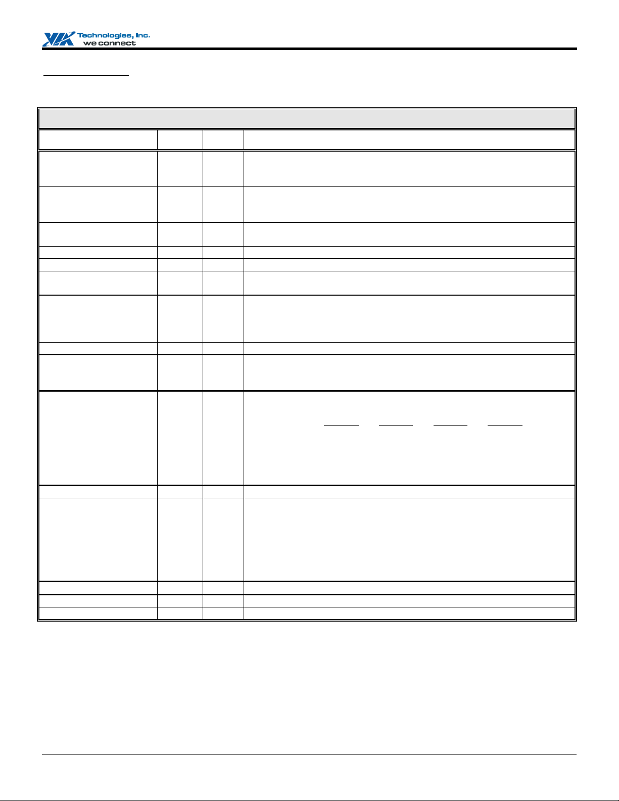
REVISION HISTORY
Document Release Date Revision Initials
1.0 5/31/00 Initial public release – removed “NDA Required” watermark
Fixed USBOC2# pin description, F0 Rx40[0], E4[6], PMIO Rx1-0[9], 45[4-0]
1.1 8/1/00 Updated feature bullets, fixed VREF pin direction, updated registers & elec/mech specs DH
1.11 8/22/00 Fixed IDE registers Rx40-45 descriptions and defaults (added Rx42) DH
1.2 11/13/00 Added note to ROMCS# pin description; Updated registers DH
1.3 12/6/00 Removed cover page watermark; Updated pin descriptions, fixed typos DH
1.31 12/11/00 Fixed definition of VCCH and GNDH pins. DH
1.4 1/19/01 Updated copyright notice & table of contents; Fixed pin descriptions and registers DH
1.5 2/1/01 Removed ACSDIN2 & fixed pin descriptions and registers DH
1.6 3/1/01 Removed ATEST and DTEST functions (reserved for internal test purposes)
Fixed GPI10-13 & GPO10-13 pin descriptions and Device 0 F4 RxE5[3-2]
Fixed note under General Purpose Inputs pin description table
Fixed STPCLK# errors in F4 Rx4C[0], PMIO Rx10[9], Rx2C[3]
Changed F5/6 Rx1C-1F to reserved and removed I/O Base 3 registers
1.7 3/19/01 Fixed heading in pin descriptions for UDMA pins
Fixed pin descriptions for JAB1, JBB1, GPI10-13, GPI28-29, GPO8-11
Fixed Device 0 Function 0 Rx40[2], Device 0 Function 4 RxE5[3-2]
1.8 4/30/01 Updated north bridge compatibility list in feature bullets
Added IRQ8# function to GPI1 pin; Added IOCHRDY to LREQ2#/GPI13 pin
Added function summary at beginning of Registers section
Added F0 Rx67[3-2] and added related notes in pin descriptions section
Removed SMB I/O register E;; Removed Temp Reading 3 from HWM I/O registers
Fixed definitions of F1 Rx43[3-0]; 50[28,20,12,4], F4 Rx55[7-6]
1.81 7/2/01 Updated company addresses; Updated Func 0 Rx4C[3:0]
Changed INIT pin to INIT# and added note to pin description
1.82 11/19/01 Fixed LAN Device ID, Elec specs FERR# input voltage; Updated marking specs DH
1.83 2/4/02 Updated logos and legal page formatting; Fixed THRM pin polarity in descriptions
Fixed figure 1 (# of serial ports); Fixed IRRX/IRTX pin descriptions
Fixed register descriptions: Port 71, Func 4 RxE5[5], PMIO Rx4[0]
1.84 2/12/02 Fixed Figure 7 PM Block Diagram to fix pdf print problem; removed “Preliminary” DH
1.85 3/11/02 Updated legal page formatting; Updated JBB1/2 and GPI17 pin descriptions DH
1.9 9/11/02 Removed incorrect register reference from PME# pin description
Fixed Device 0 Func 4 Rx42[4] description; Updated VBAT voltage specs
Added estimated power supply current / power dissipation specs based on test report data
1.91 11/4/02 Updated VIA logos on cover page and page headings to use new VIA corporate logo
Updated LAN Rx74 & added Rx78; fixed typo in electrical specs input voltage table
1.92 11/4/02 Fixed formatting problem in PDF mechanical spec page DH
2.0 11/20/02 Added ACSDIN2-3 functions & removed PCS1#; Updated GPI15, GPIO19 descriptions
Fixed typos in F2-6 Rx0-3; Updated F4 RxE4[5] and E5[7]; Updated LAN registers
2.01 12/19/02 Updated Port 61 (bits 7-6 and 3-2) and Port 92 (bits 7-6 and 3) DH
2.02 2/6/03 Fixed page 51 intro to “Super-I/O/KBC Config Index/Data Regs” step 1 Rx50[2] setting DH
2.1 4/7/03 Fixed EEDI/EEDO pin direction; fixed JEDEC spec reference in mech spec DH
2.2 4/15/03 Updated IDE Rx3C, fixed IDE Rx3D default; fixed IRTX drive DH
2.21 5/22/03 Updated Device 0 Func0 Rx59[3-2], Func4 Rx41[1-0],4C[7-4],4D[6-4], PMIO Rx10[3-0]
Updated electrical specs output pin drive table; Fixed marking specs
2.22 10/2/03 Removed IO Port Port 61 bit 6 and bit 3 VL
2.23 1/6/04 Updated Device 0 Func0 Rx54[3:0] default value VL
2.3 3/16/04 Updated D1F0 Rx6[7:5], 7[7:5], 8[0], 9[0], 0C[4], 0D[1:0], 23-20[7], 43-40[11], 6E[5:3]
and 6F[5:3]
Updated pin name for G13 and G15 in pin diagram and pin descriptons
2.31 5/10/04 Updated Device1 Function 0 Rx8B VL
2.32 9/1/04 Added a lead-free package in Mechanical Specification VL
DH
DH
DH
DH
DH
DH
DH
DH
DH
DH
VL
Revision 2.32, September 1, 2004 -i- Revision History
Page 4

VT8231 South Bridge
TABLE OF CONTENTS
REVISION HISTORY .......................................................................................................................................................................I
TABLE OF CONTENTS.................................................................................................................................................................. II
LIST OF FIGURES .........................................................................................................................................................................IV
LIST OF TABLES ...........................................................................................................................................................................IV
PRODUCT FEATURES.................................................................................................................................................................... 1
OVERVIEW....................................................................................................................................................................................... 5
PINOUTS............................................................................................................................................................................................ 7
PIN DIAGRAM ................................................................................................................................................................................ 7
PIN LISTS ....................................................................................................................................................................................... 8
PIN DESCRIPTIONS....................................................................................................................................................................... 10
REGISTERS..................................................................................................................................................................................... 31
REGISTER OVERVIEW ................................................................................................................................................................. 31
REGISTER DESCRIPTIONS ........................................................................................................................................................... 45
Legacy I/O Ports................................................................................................................................................................... 45
Keyboard Controller I/O Registers........................................................................................................................................................ 46
DMA Controller I/O Registers .............................................................................................................................................................. 48
Interrupt Controller I/O Registers.......................................................................................................................................................... 49
Timer / Counter Registers......................................................................................................................................................................49
CMOS / RTC I/O Registers................................................................................................................................................................... 50
Super-IO / KBC Configuration Index / Data Registers..................................................................................................... 51
Keyboard / Mouse Controller Configuration Registers.................................................................................................... 51
Super-I/O Configuration Registers..................................................................................................................................... 52
Super-I/O I/O Ports.............................................................................................................................................................. 55
Floppy Disk Controller Registers.......................................................................................................................................................... 55
Parallel Port Registers ........................................................................................................................................................................... 56
Serial Port 1 Registers ........................................................................................................................................................................... 57
SoundBlaster Pro Port Registers......................................................................................................................................... 58
FM Registers ......................................................................................................................................................................................... 58
Mixer Registers .....................................................................................................................................................................................58
Sound Processor Registers..................................................................................................................................................................... 58
Game Port Registers............................................................................................................................................................. 59
Fast IR Registers................................................................................................................................................................... 60
PCI Configuration Space I/O .............................................................................................................................................. 67
Device 0 Function 0 Registers - PCI to ISA Bridge ........................................................................................................... 68
PCI Configuration Space Header...........................................................................................................................................................68
ISA Bus Control .................................................................................................................................................................................... 68
PCI Master Arbitration Control............................................................................................................................................................. 70
Miscellaneous Control........................................................................................................................................................................... 71
Function Control.................................................................................................................................................................................... 72
Serial IRQ and PC/PCI DMA Control...................................................................................................................................................72
Plug and Play Control - PCI .................................................................................................................................................................. 73
Miscellaneous Control........................................................................................................................................................................... 74
Programmable Chip Select Control....................................................................................................................................................... 75
Fast IR Control...................................................................................................................................................................................... 75
ISA Decoding Control........................................................................................................................................................................... 76
Device 0 Function 1 Registers - Enhanced IDE Controller............................................................................................... 78
PCI Configuration Space Header...........................................................................................................................................................78
IDE-Controller-Specific Confiiguration Registers ................................................................................................................................ 80
Revision 2.32, September 1, 2004 -ii- Table of Contents
Page 5

VT8231 South Bridge
IDE I/O Registers.................................................................................................................................................................................. 84
Device 0 Function 2 Registers - USB Controller Ports 0-1................................................................................................ 85
PCI Configuration Space Header...........................................................................................................................................................85
USB-Specific Configuration Registers.................................................................................................................................................. 86
USB I/O Registers................................................................................................................................................................................. 87
Device 0 Function 3 Registers - USB Controller Ports 2-3................................................................................................ 88
PCI Configuration Space Header...........................................................................................................................................................88
USB-Specific Configuration Registers.................................................................................................................................................. 89
USB I/O Registers................................................................................................................................................................................. 90
Device 0 Function 4 Regs - Power Management, SMBus and HWM............................................................................... 91
PCI Configuration Space Header...........................................................................................................................................................91
Power Management-Specific PCI Configuration Registers................................................................................................................... 92
Hardware-Monitor-Specific Configuration Registers............................................................................................................................ 99
System Management Bus-Specific Configuration Registers ................................................................................................................. 99
General Purpose I/O Control Registers ............................................................................................................................................... 100
Power Management I/O-Space Registers ............................................................................................................................................ 101
System Management Bus I/O-Space Registers.................................................................................................................................... 110
Hardware Monitor I/O Space Registers............................................................................................................................................... 113
Device 0 Function 5 & 6 Registers - AC97 Audio & Modem Codecs............................................................................. 119
PCI Configuration Space Header – Function 5 Audio......................................................................................................................... 119
PCI Configuration Space Header – Function 6 Modem ......................................................................................................................120
Function 5 & 6 Codec-Specific Configuration Registers ....................................................................................................................121
I/O Base 0 Registers –Audio/Modem Scatter/Gather DMA................................................................................................................ 123
I/O Base 1 Registers – Audio FM NMI Status Registers..................................................................................................................... 127
I/O Base 2 Registers – MIDI / Game Port ........................................................................................................................................... 127
Memory Mapped I/O APIC Registers................................................................................................................................................. 128
Device 1 Function 0 Registers - LAN ................................................................................................................................ 130
PCI Configuration Space Header.........................................................................................................................................................130
LAN-Specific PCI Configuration Registers ........................................................................................................................................ 130
LAN I/O Registers............................................................................................................................................................................... 132
FUNCTIONAL DESCRIPTIONS................................................................................................................................................ 141
POWER MANAGEMENT.............................................................................................................................................................. 141
Power Management Subsystem Overview.......................................................................................................................................... 141
Processor Bus States............................................................................................................................................................................ 141
System Suspend States and Power Plane Control................................................................................................................................ 142
General Purpose I/O Ports................................................................................................................................................................... 142
Power Management Events ................................................................................................................................................................. 143
System and Processor Resume Events................................................................................................................................................. 143
Legacy Power Management Timers .................................................................................................................................................... 144
System Primary and Secondary Events ...............................................................................................................................................144
Peripheral Events................................................................................................................................................................................. 144
ELECTRICAL SPECIFICATIONS ............................................................................................................................................ 145
ABSOLUTE MAXIMUM RATINGS ............................................................................................................................................... 145
DC CHARACTERISTICS ............................................................................................................................................................. 146
POWER CHARACTERISTICS ....................................................................................................................................................... 146
OUTPUT DRIVE .......................................................................................................................................................................... 147
INPUT VOLTAGE ........................................................................................................................................................................ 147
PACKAGE MECHANICAL SPECIFICATIONS...................................................................................................................... 148
Revision 2.32, September 1, 2004 -iii- Table of Contents
Page 6

VT8231 South Bridge
LIST OF FIGURES
FIGURE 1. PC SYSTEM CONFIGURATION USING THE VT8231 ........................................................................................ 6
FIGURE 2. VT8231 BALL DIAGRAM (TOP VIEW).................................................................................................................. 7
FIGURE 3. VT8231 PIN LIST (NUMERICAL ORDER)............................................................................................................. 8
FIGURE 4. VT8231 PIN LIST (ALPHABETICAL ORDER)...................................................................................................... 9
FIGURE 5. PCI REQUEST / GRANT CONNECTIONS USING THE VT8231...................................................................... 11
FIGURE 6. STRAP OPTION CIRCUIT...................................................................................................................................... 13
FIGURE 7. POWER MANAGEMENT SUBSYSTEM BLOCK DIAGRAM......................................................................... 141
FIGURE 9. MECHANICAL SPECIFICATIONS – 376 PIN BALL GRID ARRAY PACKAGE ........................................ 148
LIST OF TABLES
TABLE 1. PIN DESCRIPTIONS .................................................................................................................................................. 10
TABLE 2. MEMORY MAPPED REGISTERS ........................................................................................................................... 31
TABLE 3. FUNCTION SUMMARY............................................................................................................................................. 31
TABLE 4. SYSTEM I/O MAP....................................................................................................................................................... 31
TABLE 5. REGISTERS ................................................................................................................................................................. 32
TABLE 6. KEYBOARD CONTROLLER COMMAND CODES .............................................................................................. 47
TABLE 7. CMOS REGISTER SUMMARY ................................................................................................................................ 50
TABLE 8 - PNP IRQ ROUTING TABLE..................................................................................................................................... 69
TABLE 9 - PNP IRQ ROUTING TABLE..................................................................................................................................... 73
Revision 2.32, September 1, 2004 -iv- Table of Contents
Page 7

VT8231 South Bridge
VT8231
SOUTH BRIDGE
PC99 COMPLIANT
NTEGRATED SUPER-I/O (FDC, LPT, COM, FIR, AND GAME PORT),
I
I
NTEGRATED FAST ETHERNET, LPC, ISA / LPC BIOS ROM,
D
IRECT SOUND AC97 AUDIO AND MC97 MODEM INTERFACE,
NTEGRATED SOUNDBLASTER PRO
I
U
LTRADMA-100/66/33 MASTER MODE EIDE CONTROLLER,
4 P
ORT USB CONTROLLER, KEYBOARD CONTROLLER, RTC,
ERIAL IRQ, SMBUS,
S
P
LUG AND PLAY, ACPI, ENHANCED POWER MANAGEMENT,
T
EMPERATURE, VOLTAGE, AND FAN-SPEED MONITORING
PRODUCT FEATURES
• Inter-operable with VIA and other Host-to-PCI Bridges
− Combine with VT8363A (Apollo KT133A) for a complete Athlon AGP 4x desktop system with 200/266 MHz FSB
− Combine with VT8361 (Apollo KLE133) or VT8365A (Apollo KM133A) for a complete Athlon system with
integrated 2D / 3D graphics
− Combine with VT82C694X (Apollo Pro133A) for a complete 66 / 100 / 133 MHz Socket370 / Slot1 AGP 4x system
− Combine with VT8601A (Apollo PLE133) or VT8605 (Apollo PM133) for a complete Socket370 / Slot1 system
with integrated 2D / 3D graphics
− Combine with VT82C598 (Apollo MVP3) for a complete Super-7 (66 / 75 / 83 / 100 MHz) AGP 2x system
− Combine with VT8501 (Apollo MVP4) for a complete Super-7 system with integrated 2D / 3D graphics
− Inter-operable with Intel or other Host-to-PCI bridges for a complete PC99 compliant PCI / AGP / LPC system
• Integrated Peripheral Controllers
− Integrated Fast Ethernet Controller with 1 / 10 / 100 Mbit capability
− Integrated USB Controller with two root hub and four function ports
− Dual channel UltraDMA-33 / 66 /100 master mode EIDE controller
− AC-link interface for AC-97 audio codec and modem codec
− HSP modem support
− Integrated SoundBlasterPro / DirectSound compatible digital audio controller
− LPC interface for Low Pin Count interface to Super-I/O or ROM
• Integrated Legacy Functions
−
Integrated Keyboard Controller with PS2 mouse support
− Integrated DS12885-style Real Time Clock with extended 256 byte CMOS RAM and Day/Month Alarm for ACPI
− Integrated Bus Controller including DMA, timer, and interrupt controller
− Serial IRQ for docking and non-docking applications
− Flash EPROM, 32Mbit (4Mbyte) EPROM and combined BIOS support
− Fast reset and Gate A20 operation
Revision 2.32, September 1, 2004 -1- Product Features
Page 8

VT8231 South Bridge
• Fast Ethernet Controller
High performance PCI master interface with scatter / gather and bursting capability
−
− Standard MII interface to Ethernet or HomePNA PHYceiver
− 1 / 10 / 100 MHz full and half duplex operation
− Transmit data buffer byte alignment for low CPU utilization
− Separate 2K byte FIFOs for receive and transmit of full Ethernet packets
− Flexible dynamically loadable EEPROM algorithm
− Physical, Broadcast, and Multicast address filtering using hashing function
− Flexible wakeup events: link status change, magic packet, unicast physical address match, predefined pattern match
− Software controllable power down
• UltraDMA-100 / 66 / 33 Master Mode PCI EIDE Controller
− Dual channel master mode PCI supporting four Enhanced IDE devices
− Transfer rate up to 100 MB/sec to cover up to PIO mode 4, multi-word DMA mode 2, and UltraDMA mode 5
− Thirty-two levels (doublewords) of prefetch and write buffers per channel
− Dual DMA engine for concurrent dual channel operation
− Bus master programming interface for SFF-8038i rev.1.0 and Windows-95 / 98 / 2000 compliant
− Full scatter gather capability
− Support ATAPI compliant devices including DVD devices
− Support PCI native and ATA compatibility modes
− Complete software driver support
• Integrated Super IO Controller
− Supports serial port, IR port, parallel port, and floppy disk controller functions
− Serial Port
− Programmable character lengths (5,6,7,8)
− Even, odd, stick or no parity bit generation and detection
− Programmable baud rate generator
− Independent transmit/receiver FIFOs
− Modem Control
− Plug and play with 96 base IO address and 12 IRQ options
− Fast IR (FIR) port
− IrDA 1.0 SIR and IrDA 1.1 FIR compliant
− IR function through the second serial port
− Infrared-IrDA (HPSIR) and ASK (Amplitude Shift Keyed) IR
− Multi-mode parallel port
− Standard mode, ECP and EPP support
− Dynamic and static switch between parallel port pinout and FDC pinout
− Plug and play with 192 base IO address, 12 IRQ and 4 DMA options
− Floppy Disk Controller
− 16 bytes of FIFO
− Data rates up to 1Mbps
− Perpendicular recording driver support
− Two FDDs with drive swap support
− Plug and play with 48 base IO address, 12 IRQ and 4 DMA options
• Low Pin Count (LPC) Bus Interface
Provides connection to external LPC I/O controllers and LPC BIOS ROMs
−
− Enables removal of legacy ISA bus and related pins
− Low pin count interface: two control pins and four address / data pins
Revision 2.32, September 1, 2004 -2- Product Features
Page 9

VT8231 South Bridge
• SoundBlaster Pro Hardware and Direct Sound Ready AC97 Digital Audio Controller
Dual full-duplex Direct Sound channels between system memory and AC97 link
−
− PCI master interface with scatter / gather and bursting capability
− 32 byte FIFO of each direct sound channel
− Host based sample rate converter and mixer
− Standard v1.0 or v2.0 AC97 Codec interface for single or cascaded AC97 Codec’s from multiple vendors
− Loopback capability for re-directing mixed audio streams into USB and 1394 speakers
− Hardware SoundBlaster Pro for Windows DOS box and real-mode DOS legacy compatibility
− Plug and play with 4 IRQ, 4 DMA, and 4 I/O space options for SoundBlaster Pro and MIDI hardware
− Hardware assisted FM synthesis for legacy compatibility
− Direct two game ports and one MIDI port interface
− Complete software driver support for Windows-95/98/2000 and Windows-NT
• MC97 HSP Modem Controller
− PCI bus master interface with scatter / gather and burst capability
− Standard AC97 codec interface for MC or AMC codec
− Wake on ring in APM or ACPI mode through AC97 link
− Supported by most HSP modem vendors
• Universal Serial Bus Controller
− USB v.1.1 and Intel Universal HCI v.1.1 compatible
− Eighteen level (doublewords) data FIFO with full scatter and gather capability
− Root hub and four function ports
− Integrated physical layer transceivers with optional over-current detection status on USB inputs
− Legacy keyboard and PS/2 mouse support
• System Management Bus Interface
− One master / slave SMBus and one slave-only SMBus
− Host interface for processor communications
− Slave interface for external SMBus masters
Revision 2.32, September 1, 2004 -3- Product Features
Page 10

VT8231 South Bridge
• Voltage, Temperature, Fan Speed Monitor and Controller
Five universal input channels for voltage or temperature sensing
−
− Two fan-speed monitoring channels
− Input channel for thermal diode in Intel™ high speed Pentium II™ / Pentium III™ CPUs
− Programmable control, status, monitor and alarm for flexible desktop management
− External thermister or internal bandgap temperature sensing
− Automatic clock throttling with integrated temperature sensing
− Internal core VCC voltage sensing
− Flexible external voltage sensing arrangement (any positive supply and battery)
• Sophisticated PC99-Compatible Mobile Power Management
− Supports both ACPI (Advanced Configuration and Power Interface) and legacy (APM) power management
− ACPI v1.0 Compliant
− APM v1.2 Compliant
− CPU clock throttling and clock stop control for complete ACPI C0 to C3 state support
− PCI bus clock run, Power Management Enable (PME) control, and PCI/CPU clock generator stop control
− Supports multiple system suspend types: power-on suspends with flexible CPU/PCI bus reset options,
suspend to DRAM, and suspend to disk (soft-off), all with hardware automatic wake-up
− Multiple suspend power plane controls and suspend status indicators
− One idle timer, one peripheral timer and one general purpose timer, plus 24/32-bit ACPI compliant timer
− Normal, doze, sleep, suspend and conserve modes
− Global and local device power control
− System event monitoring with two event classes
− Primary and secondary interrupt differentiation for individual channels
− Dedicated input pins for power and sleep buttons, external modem ring indicator, and notebook lid open/close for
system wake-up
− Multiple internal and external SMI sources for flexible power management models
− One programmable chip select and one microcontroller chip select
− Enhanced integrated real time clock (RTC) with date alarm, month alarm, and century field
− Thermal alarm on either external or any combination of three internal temperature sensing circuits
− Hot docking support
− I/O pad leakage control
• Plug and Play Controller
− PCI interrupts steerable to any interrupt channel
− Steerable interrupts for integrated peripheral controllers: USB, floppy, serial, parallel, audio, soundblaster, MIDI
− Steerable DMA channels for integrated floppy, parallel, and soundblaster pro controllers
− One additional steerable interrupt channel for on-board plug and play devices
− Microsoft Windows 2000
BIOS compliant
TM
, Windows 98SETM, Windows 98TM, Windows NTTM, Windows 95
• Built-in NAND-tree pin scan test capability
• 0.30um, 3.3V, low power CMOS process
• Single chip 27x27 mm, 376 pin BGA
TM
and plug and play
Revision 2.32, September 1, 2004 -4- Product Features
Page 11

VT8231 South Bridge
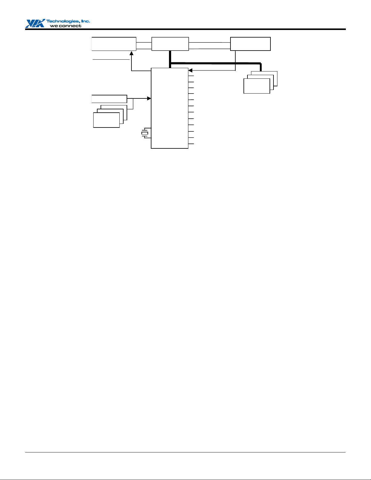
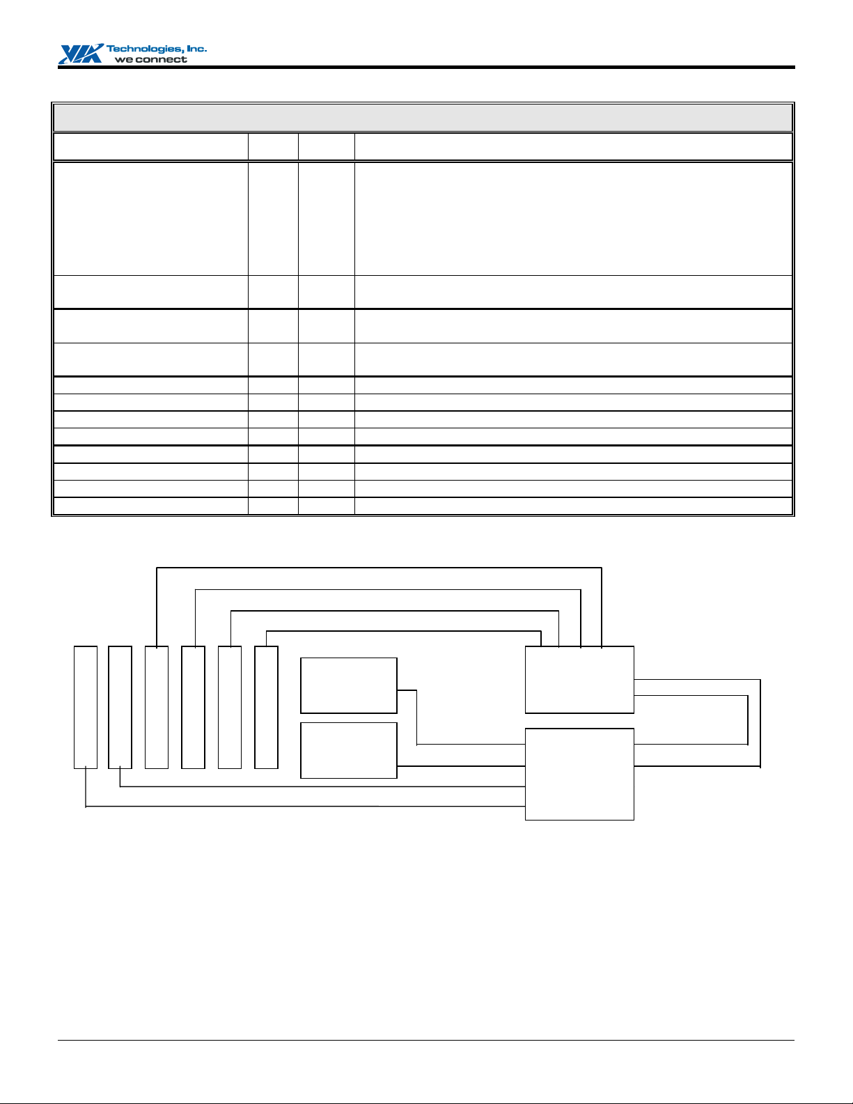
OVERVIEW
The VT8231 South Bridge is a high integration, high performance, power-efficient, and high compatibility device that supports
Intel, AMD, and VIA / Cyrix based processor to PCI bus bridge functionality to make a complete Microsoft PC99-compliant PCI /
LPC system. The VT8231 includes standard intelligent peripheral controllers:
a) Master mode enhanced IDE controller with dual channel DMA engine and interlaced dual channel commands. Dedicated
FIFO coupled with scatter and gather master mode operation allows high performance transfers between PCI and IDE
devices. In addition to standard PIO and DMA mode operation, the VT8231 also supports the UltraDMA-33, 66, and 100
standards to allow reliable data transfer rates up to 100 MB/sec throughput. The IDE controller is SFF-8038i v1.0 and
Microsoft Windows-family compliant.
b) Integrated LAN Fast Ethernet controller (MAC) with Media Independent Interface (MII) to external Ethernet PHY or
HomePNA PHY. The LAN controller operates at 1 / 10 / 100 Mbit/sec transfer rates using either full and half duplex
operation and has separate 2Kbyte FIFOs for receive and transmit of full ethernet packets. The internal high-performance
PCI interface has scatter / gather and bursting capability and can align bytes in the transmit data buffer to reduce CPU
utilization. The LAN interface can perform address filtering on physical, broadcast, and multicast packets. The interface can
also be configured for system wake up on link status change, receipt of magic packet, unicast physical address match on
incoming packets, and predefined pattern match in the incoming data.
c) LPC (Low Pin Count) interface for BIOS ROM plus optional conventional BIOS ROM support
d) Universal Serial Bus controller that is USB v1.1 and Universal HCI v1.1 compliant. The VT8231 includes the root hub with
four function ports with integrated physical layer transceivers. The USB controller allows hot plug and play and isochronous
peripherals to be inserted into the system with universal driver support. The controller also implements legacy keyboard and
mouse support so that legacy software can run transparently in a non-USB-aware operating system environment.
e) Keyboard controller with PS2 mouse support
f) Real Time Clock with 256 byte extended CMOS. In addition to standard RTC functionality, the integrated RTC also
includes the date alarm, century field, and other enhancements for compatibility with the ACPI standard.
g) Notebook-class power management functionality compliant with ACPI and legacy APM requirements. Multiple sleep states
(power-on suspend, suspend-to-DRAM, and suspend-to-Disk) are supported with hardware automatic wake-up. Additional
functionality includes event monitoring, CPU clock throttling and stop (Intel processor protocol), PCI bus clock stop control,
modular power, clock and leakage control, hardware-based and software-based event handling, general purpose I/O, chip
select and external SMI.
h) Hardware monitoring subsystem for managing system / motherboard voltage levels, temperatures, and fan speeds
i) Full System Management Bus (SMBus) interface with one master / slave port and one slave-only port
j) 16550-compatible serial I/O port with “Fast-IR” infrared communications port option.
k) Integrated PCI-mastering dual full-duplex direct-sound AC97-link-compatible sound system. Hardware soundblaster-pro
and hardware-assisted FM blocks are included for Windows DOS box and real-mode DOS compatibility. Loopback
capability is also implemented for directing mixed audio streams into USB and 1394 speakers for high quality digital audio.
l) Game port and MIDI port
m) Standard floppy disk drive interface
n) ECP/EPP-capable parallel port with floppy disk controller pinout option
o) Serial IRQ for docking and non-docking applications
p) Plug and Play controller that allows complete steerability of all PCI interrupts and internal interrupts to any interrupt channel.
One additional steerable interrupt channel is provided to allow plug and play and reconfigurability of on-board peripherals
for Windows family compliance.
Revision 2.32, September 1, 2004 -5- Overview
Page 12
VT8231 South Bridge
CPU / Cache
Sideband Signals:
Init / CPUreset
IRQ / NMI
SMI / StopClk
FERR / IGNNE
SLP# (Slot-1)
Boot ROM
Onboard
LPC I/O
CA
CD
LPC
RTC
Crystal
North Bridge
VT8231
376 BGA
MA/Command
MD
PCI
SMB
USB Ports 0-3
Keyboard / Mouse
MIDI / Game Ports
Parallel Port
Serial Port
Infrared Comm Port
IDE Primary and Secondary
Floppy Disk Interface
AC97 Link
Hardware Monitor Inputs
GPIO, Power Control, Reset
Fast Ethernet Interface
System Memory
DIMM Module ID
Expansion
Cards
Figure 1. PC System Configuration Using the VT8231
Revision 2.32, September 1, 2004 -6- Overview
Page 13
VT8231 South Bridge
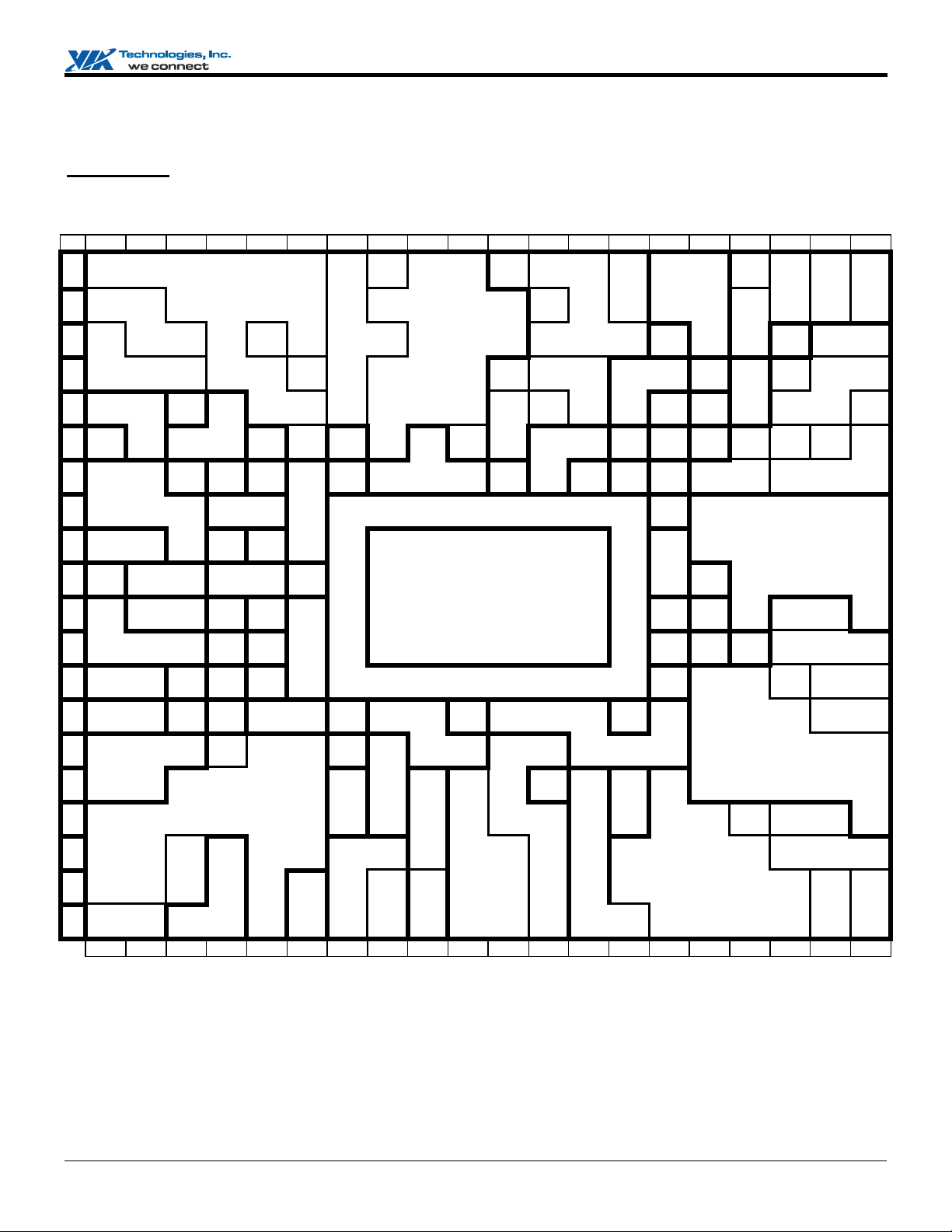
PINOUTS
Pin Diagram
Figure 2. VT8231 Ball Diagram (Top View)
Key 1 2 3 4 5 6 7 8 9 10 11 12 13 14 15 16 17 18 19 20
AD
AD
AD
AD
AD
AD
DEV
CBE
A
30
31
26
24
21
16
SEL#
PINT
PINT
AD
AD
AD
B
B#
A#
28
25
PREQ
PINT
PINT
C
H#
D#
PGNT
PREQ
D
L#
V
E
BAT
JB
F
B1
AC
G
SYNC
AC
H
SDIN0
JA X JB Y AC
J
VREF
K
UIC 5 DTD + DTD - UIC
L
UIC 1 UIC 3 UIC 2 KB
M
KB
N
DT
SUSA
P
#/strap
SMB
R
CK2
SMB
T
DT1
PME#
U
CPU
V
MISS
EXT
W
SMI#
GPIO D GPIO A APIC
Y
1 2 3 4 5 6 7 8 9 10 11 12 13 14 15 16 17 18 19 20
Note: Some of the pins above have alternate functions and alternate names. The table above contains only one name (usually the most often used function), but the
pin lists and pin descriptions contain all names.
PGNT
L#
PWR
GD
RSM
RST#
AC
RST#
AC
SDIN1
BCLK
FAN 1 FAN2
SLPB#
MS
CK
SUS
B#
SMB
DT2
SMB
ALRT#
LOW#
PWR
BTN#
LID
IRQ8#
SUS
CLK
AD
C#
27
AD
H#
29
RTC
PCI
X1
RST#
INTR
GPI 0 RTC
UDR#
JA
MSI
B1
AC
SUS
C#
AOL
GPI
CK1
BAT
CLK
JB
B2
MSO
JA Y JB
4
CK
MS
DT
CPU
STP#
GPO 0 PCK
PCI
STP#
RST
WSC#
D0
APIC
D1
SDO
SMB
RING # CPU
GPI1
GPIO E APIC
PCS1#
SDIN2
HWM
HWM
RUN#
FERR
AD
23
18 T RDY#
CBE
AD
3#
19 I RDY#
AD
CBE
20
AD
22
X2
JA
B2
GPIO
C
X
GND
VCC
SUS
ST#
VCC
SUS
NMI
#
INIT # STP
A20
M#
SMI#
STOP # AD
2#
AD
SERR # AD
17
FRM#
VCC
GND VCC VCC VCC GND VCC
VCC
VCC
VCC J GND GND GND GND GND GND J VCC
GND K GND GND GND GND GND GND K VCC
VCC L GND GND GND GND GND GND L GND
VCC M GND GND GND GND GND GND M VCC
VCC N7 8 9 10 11 12 13 N14 GND
VCC
SUS
INTR
IGN
NE#
SLP#
CLK# L AD3 L AD0
MCCS
#/strap L AD2 L FRM#
PCS0#
/strap L AD1 L DRQ#
H7 8 9 10 11 12 13 H14 GND
GND VCC VCC GND VCC VCC VCC GND VCC
VCC
IO
W#
IO
R#
AD 9 AD
1#
AD
AD
15
PAR
14
13
AD
11
IR
TX
IR
RX2
IR
RX
AD 4 AD 1 P
10
AD
AD 6 AD 0 PD 1 PD 4 PD 7 USB
12
AD 7 AD 2 PD 0 SLCT
AD 8 AD 3 AUTO
CBE
VCC
VCC VCC
ROM
SPKR
MEM
MEM
CS#
SER
IRQ
R#
W#
0#
HG2#
GPO9
LR1#
GPI12
LG2#
GPO11
LR2#
RDY
LG1#
GPO10
5
ERR#
HR2#
GPI11
HG1#
GPO8
HR1#
STR#
INIT#
FD#
SD 6 SD
SD
7
SD
5
PD 2 PD
6
PD
5
PE DSR# DCD#
IN#
PD
SLCT RXD
3
VCC VCC
GND
LAN
VCC VCC VCC
0
SA17
OSC
/strap
SD
SA
4
18
SA
SD
19
1
LA
SD
20
2
SD
LA
3
21
BUSY RTS# DTR#
ACK# TXD CTS#
RI#
CLK
USB
OC1#
EE
VCC
CK
USB
GND
USB
GND
IRQ
14
IRQ
15
SA5
SDD5
SA9
SDD9
SA16
/strap
VCC
VCC
LAN
SA8
SDD8
SA7
SDD7
SA11
SDD11
SA4
SDD4
SA10
SDD10
VCC
MII
M
CRS M COL
TRK
00#
MTR
1#
VCC
MII
VCC
PLL
GND
PLL
PD
D10
PD
D4
PD
D1
PD
D0
SA6
SDD6
SA2
SDD2
SA12
SDD12
SA3
SDD3
USB
OC0#
USB
P3-
USB
P3+
EE
DO
EE
DI
MTX
CLK
WRT
PRT#
DS
0#
DRV
DEN1
DRV
DEN0
PCI
CLK
PD
D5
PD
D11
PD
D14
PD
D15
SD
DRQ
SA14
SDD14
SA1
SDD1
SA13
SDD13
USB
P0-
USB
P0+
EE
CS#
MD
IO
MRX
D1
MRX
ERR
MTX
D1
DSK
CHG#
STEP#
MTR
0#
PDCS
1#
PD
A1
PD
IOR#
PD
D8
PD
D7
PD
D13
SDCS
1#
SD
A1
SA15
SDD15
SA0
SDD0
USB
USB
P1-
P2-
USB
USB
P1+
P2+
MRX
MD
CLK
CK
MRX
MRX
D3
D2
MRX
MRX
D0
DV
MTX
MTX
ENA
D0
MTX
MTX
D2
D3
HD
R
DATA#
SEL#
W
DATA#W GATE#
DS
DIR#
1#
PDCS
RDY
DRQ
SDCS
IOR#
IOW#
3#
PD
A0
PD
PD
PD
D9
PD
D3
3#
SD
A0
SD
SD
IN
DEX#
PD
A2
PD
DACK#
PD
IOW#
PD
D6
PD
D12
PD
D2
SD
A2
SD
DACK#
SD
RDY
Revision 2.32, September 1, 2004 -7- Pin Diagrams
Page 14
VT8231 South Bridge
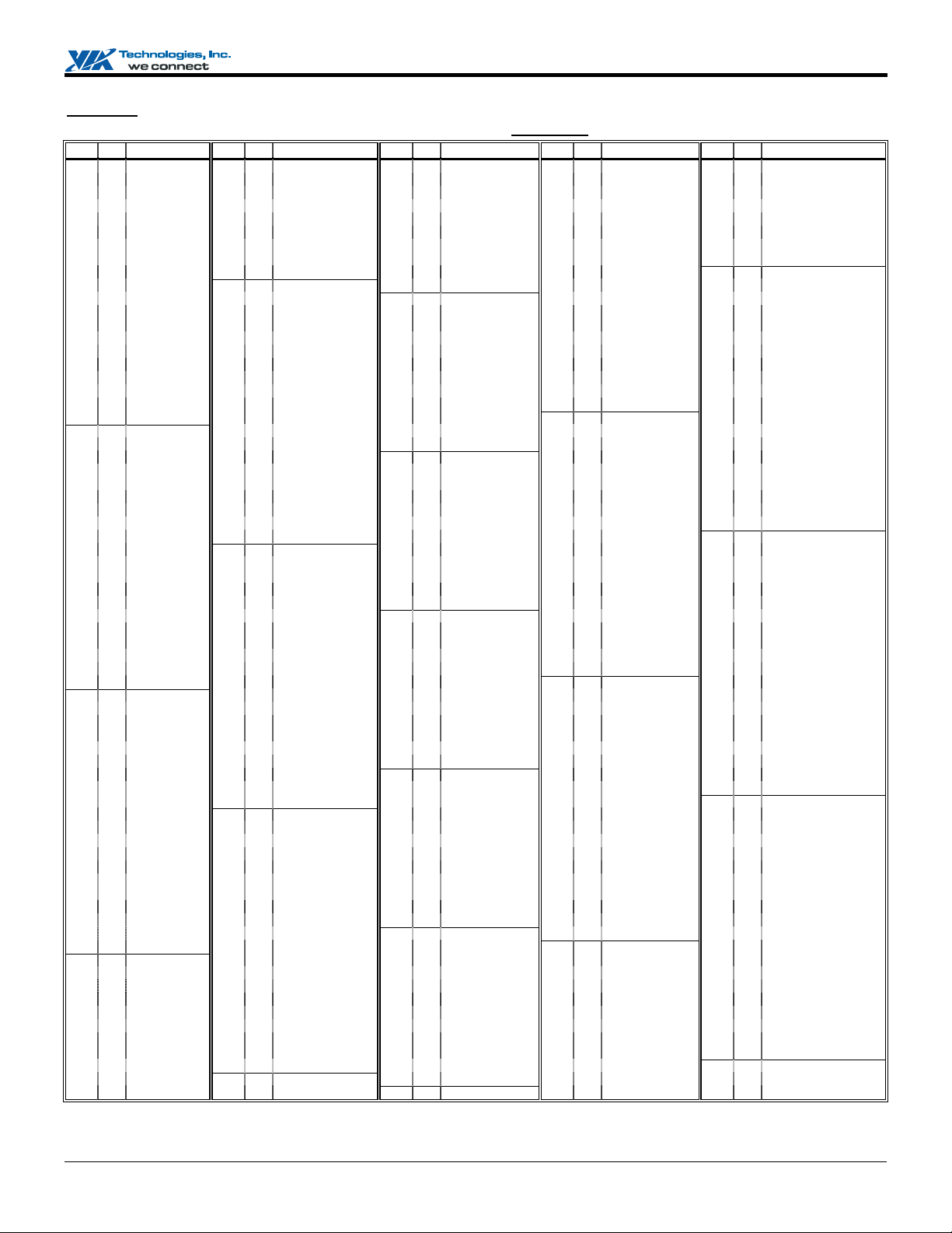
Pin Lists
Figure 3. VT8231 Pin List (Numerical Order)
Pin Pin Name Pin Pin Name Pin Pin Name Pin Pin Name Pin Pin Name
A01 IO AD30 D12 IO SLCTIN#/STEP# H03 O ACSDOUT P02 O SUSB# / GPIO2 U13 IO SA18
A02 IO AD31 D13 I PE / WDATA# H04 I JBB2 / GPO13 P03 I AOLGPI/THRM/I17 U14 I IRQ15
A03 IO AD26 D14 I DSR# H05 I JAB2 / GPO12 P04 O CPUSTP# / GPO5 U15 IO SA07 / SDD07
A04 IO AD24 D15 I DCD#
A05 IO AD21 D16 I USBOC1#
A06 IO AD16 D17 I EEDO H16 I TRK00#
A07 IO DEVSEL# D18 IO MDIO H17 I WRTPRT#
A08 IO CBE1# D19 I MRXD3 H18 I DSKCHG#
A09 IO AD09 D20 I MRXD2 H19 O HDSEL#
A10 IO AD05
A11 IO STROBE# E02 I PWRGD J01 I JAX
A12 IO PD2 / WRTPRT# E03 I RTCX1 J02 I JBY
A13 IO PD6 E04 O PCIRST# J03 I ACBITCLK
A14 I BUSY / MTR1# E05 IO AD22 J04 O MSO
A15 O RTS# E06 IO AD17 J05 IO GPIOC/IO25/CHSIO P16 IO PDD04 V07 IO LAD3
A16 O DTR# E07 I SERR#
A17 I USBOC0# E08 IO AD13
A18 IO USBP0- E09 IO AD08 J16 O MTR1# P19 I PDDRQ V10 O LGNT2# / GPO11
A19 IO USBP1- E10 IO AD03 J17 O DS0# P20 O PDIOW# V11 I HREQ2# / GPI11
A20 IO USBP2- E11 IO AUTOFD#/DRV0 J18 O STEP# R01 IO SMBCK2 / GPIO27 V12 IO SD01
B01 I PINTB# E12 IO PD3 / RDATA# J19 O WDATA# R02 IO SMBDT2 / GPIO26 V13 IO SA19
B02 I PINTA# E13 I SLCT/WGATE# J20 O WGATE# R03 IO SMBCK1 V14 IO SA05 / SDD05
B03 IO AD28 E14 I RXD
B04 IO AD25
B05 IO AD23 E16 O EECK K03 I FAN2/SLPB#/IO18 R06 OD INTR V17 IO SA14 / SDD14
B06 IO AD18 E17 O EEDI K04 I JAY
B07 IO TRDY# E18 I MRXD1 K05 I JBX R08 O IRTX / GPO14 V19 O SDA0
B08 IO AD15 E19 I MRXD0
B09 IO AD10 E20 I MRXDV
B10 IO AD04 F01 I JBB1 / GPI29
B11 IO AD01 F02 I RSMRST# K17 O DRVDEN1 R12 IO SD00 W03 IO GPIOE / GPIO31
B12 IO PINIT# / DIR# F03 I INTRUDER#/GPI8 K18 O MTR0#
B13 IO PD5 F04 I GPI0 K19 O DS1#
B14 I ACK# / DS1# F05 O RTCX2 K20 O DIR#
B15 O TXD F06 IO FRAME# L01 AI UIC5 R16 IO PDD01 W07 IO LAD2
B16 I CTS#
B17 IO USBP3- F08 IO AD11 L03 AI DTD- R18 IO PDD07 W09 IO MEMR#
B18 IO USBP0+
B19 IO USBP1+ F10 IO CBE0#
B20 IO USBP2+ F11 I ERROR#/HDSEL#
C01 O PREQH#
C02 I PINTD#
C03 I PINTC#
C04 IO AD27
C05 IO CBE3#
C06 IO AD19 F17 I MTXCLK L20 I INDEX# T07 IO IOW# / GPIO23 W18 IO SA15 / SDD15
C07 IO IRDY# F18 I MRXERR M01 AI UIC1 T08 I IRRX2 / GPIOB W19 O SDIOR#
C08 IO PAR F19 O MTXENA M02 AI UIC3 T09 O ROMCS# / KBCS# W20 O SDDACK#
C09 IO AD12 F20 O MTXD0 M03 AI UIC2 T10 O HGNT2# / GPO9 Y01 IO GPIOD / GPIO30
C10 IO AD06 G01 O ACSYNC M04 IO KBCK / A20G T11 IO SD07 Y02 IO GPIOA / GPIO24
C11 IO AD00 G02 O ACRST#
C12 IO PD1 / TRK00# G03 I JAB1 / GPI28
C13 IO PD4 / DSKCHG# G04 I MSI
C14 IO PD7 G05 O ACSDIN2 / GPIO19
C15 I USBCLK
C16 I RI#
C17 IO USBP3+
C18 O EECS#
C19 I MRXCLK
C20 O MDCK
D01 I PGNTL#
D02 O PREQL#
D03 I PGNTH#
D04 IO AD29
D05 IO AD20 G16 I MCRS
D06 IO CBE2# G17 I MCOL N16 IO PDD10 U07 IO IOR# / GPIO22 Y18 IO SA00 / SDD00
D07 IO STOP# G18 O MTXD1 N17 IO PDD05 U08 I IRRX / GPO15 Y19 O SDIOW#
D08 IO AD14 G19 O MTXD2 N18 O PDIOR# U09 O SPKR Y20 I SDRDY
D09 IO AD07 G20 O MTXD3 N19 I PDRDY U10 I LREQ1# / GPI12
D10 IO AD02 H01 I ACSDIN0 N20 O PDDACK# U11 IO SD05
D11 IO PD0 / INDEX# H02 I ACSDIN1 P01 O SUSA#/GPO1/strapU12 IO SD04
E01 P VBAT
E15 P VCCUSB
F07 P VCC
F09 P VCC
F12 P VCC L15 P GND
F13 P VCC L16 P VCCPLL
F14 P GNDUSB
F15 P VCC
F16 P VCCMII
G06 P VCC
G07 P GND
G08 P VCC
G09 P VCC
G10 P VCC
G11 P GND
G12 P VCC
G13 P GNDLAN
G14 P GND
G15 P VCCLAN N06 P VCC
H06 P VCC P05 P VCCSUS
H15 P GND P06 P VCCSUS
H20 I RDATA#
J06 P VCC
J15 P VCC
K01 O VREF
K02 I FAN1 R05 IO PCKRUN# V16 IO SA02 / SDD02
K06 P GND R09 P VCC
K15 P VCC R10 P VCC
K16 P VCCMII
L02 AI DTD+ R17 IO PDD14 W08 O LFRAME#
L04 AI UIC4 R19 IO PDD09 W10 I LREQ2#/GPI13/OCHRDY
L05 P GNDHWM
L06 P VCC
L17 O DRVDEN0 T04 O PCISTP# / GPO6 W15 IO SA04 / SDD04
L18 O PDCS1# T05 OD NMI W16 IO SA12 / SDD12
L19 O PDCS3# T06 OD IGNNE# W17 IO SA01 / SDD01
M05 P VCCHWM
M06 P VCC
M15 P VCC
M16 P GNDPLL
M17 I PCICLK T16 IO PDD00 Y07 IO LAD1
M18 O PDA1 T17 IO PDD15 Y08 I LDRQ# / GPI15 / SDIN3
M19 O PDA0 T18 IO PDD13 Y09 IO MEMW#
M20 O PDA2 T19 IO PDD03 Y10 O LGNT1# / GPO10
N01 IO KBDT / KBRC T20 IO PDD12 Y11 I HREQ1# / GPI10
N02 IO MSCK / IRQ1 U01 I PME# / GPI6 Y12 IO SD03
N03 O SUSC# / GPO U02 I PWRBTN# Y13 IO LA21/OC3#/IO21
N04 IO MSDT / IRQ12 U03 I RING# / GPI3 Y14 IO SA16 / strap
N05 O SUSST1# / GPO3 U04 OD CPURST Y15 IO SA10 / SDD10
N15 P GND
P07 P GND
P08 P VCC
P09 P VCC
P10 P GND
P11 P VCC
P12 P VCC
P13 P VCC
P14 P GND
P15 P VCC
P17 IO PDD11 V08 IO LAD0
P18 IO PDD08 V09 I SERIRQ
R04 O SLOWCLK / O0 V15 IO SA11 / SDD11
R07 P VCC
R11 IO SD06 W02 O SUSCLK / GPO4
R13 P VCC
R14 P VCC
R15 P VCC
R20 IO PDD06 W11 O HGNT1# / GPO8
T01 IO SMBDT1 W12 IO SD02
T02 I SMBALRT# / GPI7 W13 IO LA20/OC2#/IO20
T03 I BATLOW# / GPI5 W14 IO SA09 / SDD09
T12 I OSC Y03 I APICCLK / GPI9
T13 IO SA17 / strap Y04 O APICD1 / GPO29
T14 I IRQ14 Y05 OD SMI#
T15 IO SA08 / SDD08 Y06 O PCS# / GPO16
U05 I FERR# Y16 IO SA03 / SDD03
U06 OD SLP# / GPO7 Y17 IO SA13 / SDD13
Center GND pins (24 pins): J8-J13, K8-K13, L8-L13, M8-M13
U16 IO SA06 / SDD06
U17 I SDDRQ
U18 O SDCS1#
U19 O SDCS3#
U20 IO PDD02
V01 I CPUMISS / GPI16
V02 I LID / GPI4
V03 I GPI1 / IRQ8#
V04 I WSC# / GPI24
V05 OD INIT#
V06 OD STPCLK#
V18 O SDA1
V20 O SDA2
W01 IOD EXTSMI# / GPI2
W04 O APICD0 / GPIO28
W05 OD A20M#
W06 O MCCS#/O17/strap
Revision 2.32, September 1, 2004 -8- Pin Lists
Page 15
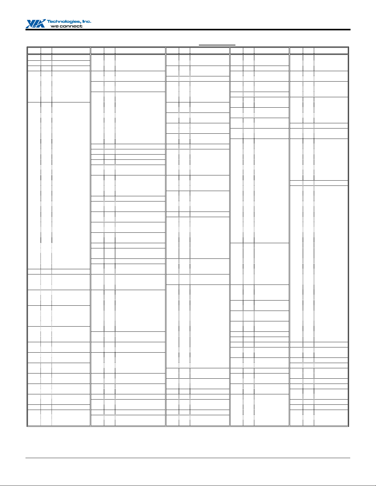
VT8231 South Bridge
K
K
K
K
K
K
Q
Figure 4. VT8231 Pin List (Alphabetical Order)
Pin Pin Name Pin Pin Name Pin Pin Name Pin Pin Name Pin Pin Name
W05 OD A20M# D17 I EEDO C20 O MDCK C03 I PINTC# P01 O SUSA# / GPO1
J03 I ACBITCLK F11 I ERROR#/HDSEL# D18 IO MDIO C02 I PINTD# P02 O SUSB# / GPO2
B14 I ACK# / DS1# W01 IOD EXTSMI# / GPI2 W09 IO MEMR# U01 I PME# / GPI6 N03 O SUSC#
G02 O ACRST# K02 I FAN1 Y09 IO MEMW# C01 O PREQH# W02 O SUSCL
H01 I ACSDIN0 K03 I FAN2/SLPB#/IO18 C19 I MRXCL
H02 I ACSDIN1 U05 I FERR# E19 I MRXD0 U02 I PWRBTN# B07 IO TRDY#
G05 O ACSDIN2 / GPIO19 F06 IO FRAME# E18 I MRXD1 E02 I PWRGD H16 I TRK00#
H03 O ACSDOUT
G01 O ACSYNC
C11 IO AD00
B11 IO AD01
D10 IO AD02
E10 IO AD03
B10 IO AD04
A10 IO AD05
C10 IO AD06
D09 IO AD07
E09 IO AD08
A09 IO AD09
B09 IO AD10
F08 IO AD11
C09 IO AD12 F04 I GPI0 G20 O MTXD3 V14 IO SA05 / SDD05 B20 IO USBP2+
E08 IO AD13 V03 I GPI1 / IRQ8# F19 O MTXENA U16 IO SA06 / SDD06 B17 IO USBP3D08 IO AD14 Y02 IO GPIOA / GPIO24 T05 OD NMI U15 IO SA07 / SDD07 C17 IO USBP3+
B08 IO AD15 J05 IO GPIOC / GPIO25 T12 I OSC T15 IO SA08 / SDD08
A06 IO AD16 Y01 IO GPIOD / GPIO30 C08 IO PAR W14 IO SA09 / SDD09
E06 IO AD17 W03 IO GPIOE R05 IO PCKRUN# Y15 IO SA10 / SDD10
B06 IO AD18 H19 O HDSEL# M17 I PCICL
C06 IO AD19 W11 O HGNT1# / GPO8 E04 O PCIRST# W16 IO SA12 / SDD12
D05 IO AD20 T10 O HGNT2# / GPO9 T04 O PCISTP# / GPO6 Y17 IO SA13 / SDD13
A05 IO AD21 Y11 I HREQ1# / GPI10 Y06 O PCS# / GPO16 V17 IO SA14 / SDD14
E05 IO AD22 V11 I HREQ2# / GPI11 D11 IO PD0 / INDEX# W18 IO SA15 / SDD15
B05 IO AD23 T06 OD IGNNE# C12 IO PD1 / TRK00# Y14 IO SA16 / strap
A04 IO AD24 L20 I INDEX# A12 IO PD2 / WRTPRT# T13 IO SA17 / strap
B04 IO AD25 V05 OD INIT# E12 IO PD3 / RDATA# U13 IO SA18
A03 IO AD26 R06 OD INTR C13 IO PD4 / DSKCHG# V13 IO SA19
C04 IO AD27 F03 I INTRUDER#/GPI8 B13 IO PD5 R12 IO SD00
B03 IO AD28 U07 IO IOR# / GPIO22 A13 IO PD6 V12 IO SD01
D04 IO AD29 T07 IO IOW# / GPIO23 C14 IO PD7 W12 IO SD02
A01 IO AD30 C07 IO IRDY# M19 O PDA0 Y12 IO SD03
A02 IO AD31 T14 I IRQ14 M18 O PDA1 U12 IO SD04
P03 I AOLGPI/THRM/I17 U14 I IRQ15 M20 O PDA2 U11 IO SD05
Y03 O APICLK / GPI9 U08 I IRRX / GPO15 L18 O PDCS1# R11 IO SD06
W04 O APICD0 / GPIO28 T08 I IRRX2 / GPIOB L19 O PDCS3# T11 IO SD07
Y04 O APICD1 / GPIO29 R08 O IRTX / GPO14 T16 IO PDD00 V19 O SDA0
E11 IO AUTOFD# / DRV0 G03 I JAB1 / GPI28 R16 IO PDD01 V18 O SDA1
T03 I BATLOW# / GPI5 H05 I JAB2 / GPO12 U20 IO PDD02 V20 O SDA2
A14 I BUSY / MTR1# J01 I JAX T19 IO PDD03 U18 O SDCS1#
F10 IO CBE0# K04 I JAY P16 IO PDD04 U19 O SDCS3#
A08 IO CBE1# F01 I JBB1 / GPI29 N17 IO PDD05 W20 O SDDACK#
D06 IO CBE2# H04 I JBB2 / GPO13 R20 IO PDD06 U17 I SDDRQ
C05 IO CBE3# K05 I JBX R18 IO PDD07 W19 O SDIOR#
V01 I CPUMISS / GPI16 J02 I JBY P18 IO PDD08 Y19 O SDIOW#
U04 OD CPURST M04 IO KBCK / A20G R19 IO PDD09 Y20 I SDRDY
P04 O CPUSTP# / GPO5 N01 IO KBDT / KBRC N16 IO PDD10 V09 I SERIRQ
B16 I CTS# W13 IO LA20 / OC2# / GPIO20 P17 IO PDD11 E07 I SERR#
D15 I DCD# Y13 IO LA21 / OC3# / GPIO21 T20 IO PDD12 E13 I SLCT/WGATE#
A07 IO DEVSEL# V08 IO LAD0 T18 IO PDD13 D12 IO SLCTIN#/STEP#
K20 O DIR# Y07 IO LAD1 R17 IO PDD14 R04 O SLOWCLK / O0
L17 O DRVDEN0 W07 IO LAD2 T17 IO PDD15 U06 OD SLP# / GPO7
K17 O DRVDEN1 V07 IO LAD3 N20 O PDDACK# T02 I SMBALRT# / I7
J17 O DS0# Y08 I LDRQ#/ / GPI15 / SDIN3 P19 I PDDR
K19 O DS1# W08 O LFRAME# N18 O PDIOR# R01 IO SMBCK2 / IO27
H18 I DSKCHG# Y10 O LGNT1# / GPO10 P20 O PDIOW# T01 IO SMBDT1
D14 I DSR# V10 O LGNT2# / GPO11 N19 I PDRDY R02 IO SMBDT2 / IO26 J19 O WDATA#
L02 AI DTD+ V02 I LID / GPI4 D13 I PE / WDATA# Y05 OD SMI# J20 O WGATE#
L03 AI DTD– U10 I LREQ1# / GPI12 D03 I PGNTH# U09 O SPKR H17 I WRTPRT#
A16 O DTR# W10 I LREQ2#/GPI13/IOCHRD D01 I PGNTL# J18 O STEP# V04 I WSC# / GPI14
E16 O EECK W06 O MCCS#/O17/strap B12 IO PINIT# / DIR# D07 IO STOP#
C18 O EECS# G17 I MCOL B02 I PINTA# V06 OD STPCLK#
E17 O EEDI G16 I MCRS B01 I PINTB# A11 IO STROBE#
G07 P GND
G11 P GND
G14 P GND
H15 P GND
K06 P GND
L15 P GND
N15 P GND
P07 P GND
P10 P GND
P14 P GND
L05 P GNDHWM
M16 P GNDPLL
G13 P GNDLAN
F14 P GNDUSB
D20 I MRXD2 H20 I RDATA# B15 O TXD
D19 I MRXD3 C16 I RI# M01 I UIC1
E20 I MRXDV U03 I RING# / GPI3 M03 I UIC2
F18 I MRXERR T09 O ROMCS#/KBCS# M02 I UIC3
N02 IO MSCK / IRQ1 F02 I RSMRST# L04 I UIC4
N04 IO MSDT / IRQ12 E03 I RTCX1 L01 I UIC5
G04 I MSI F05 O RTCX2 C15 I USBCL
J04 O MSO A15 O RTS# A17 I USBOC0#
18 O MTR0# E14 I RXD D16 I USBOC1#
J16 O MTR1# Y18 IO SA00 / SDD00 A18 IO USBP0F17 I MTXCL
F20 O MTXD0 V16 IO SA02 / SDD02 A19 IO USBP1G18 O MTXD1 Y16 IO SA03 / SDD03 B19 IO USBP1+
G19 O MTXD2 W15 IO SA04 / SDD04 A20 IO USBP2-
Center GND pins (24 pins): J8-J13, K8-K13, L8-L13, M8-M13
D02 O PREQL# N05 O SUSST1# / GPO3
W17 IO SA01 / SDD01 B18 IO USBP0+
E01 P VBAT
F07 P VCC
V15 IO SA11 / SDD11
R03 IO SMBCK1
F09 P VCC
F12 P VCC
F13 P VCC
F15 P VCC
G06 P VCC
G08 P VCC
G09 P VCC
G10 P VCC
G12 P VCC
H06 P VCC
J06 P VCC
J15 P VCC
K15 P VCC
L06 P VCC
M06 P VCC
M15 P VCC
N06 P VCC
P08 P VCC
P09 P VCC
P11 P VCC
P12 P VCC
P13 P VCC
P15 P VCC
R07 P VCC
R09 P VCC
R10 P VCC
R13 P VCC
R14 P VCC
R15 P VCC
M05 P VCCHWM
F16 P VCCMII
K16 P VCCMII
L16 P VCCPLL
G15 P VCCLAN
P05 P VCCSUS
P06 P VCCSUS
E15 P VCCUSB
K01 O VREF
Revision 2.32, September 1, 2004 -9- Pin Lists
Page 16
VT8231 South Bridge
Pin Descriptions
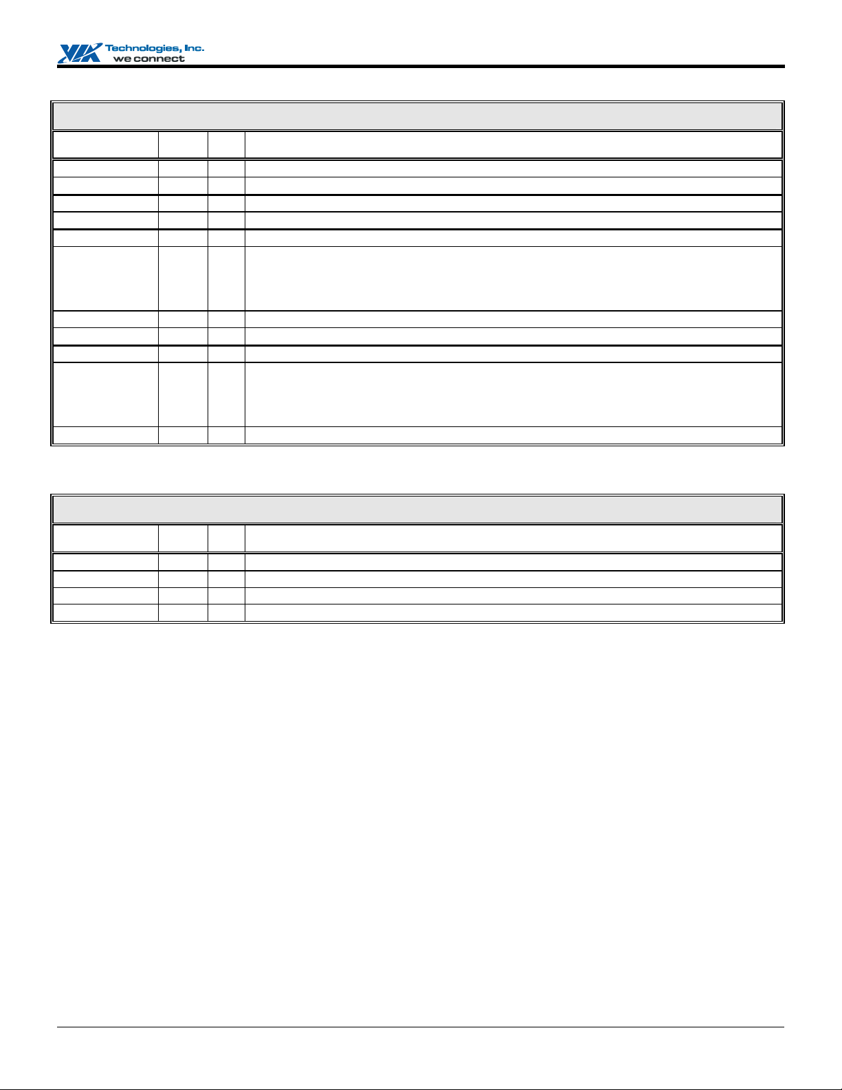
Table 1. Pin Descriptions
PCI Bus Interface
Signal Name Pin # I/O Signal Description
AD[31:0]
C/BE[3:0]#
FRAME#
IRDY#
TRDY#
STOP#
DEVSEL#
PAR
SERR#
PINTA-D#
PCICLK
PCKRUN#
PCIRST#
PCISTP# / GPO6 T4 O
CPUSTP# / GPO5 P4 O
(see pin
list)
C5, D6,
A8, F10
F6 IO Frame. Assertion indicates the address phase of a PCI transfer. Negation
C7 IO Initiator Ready. Asserted when the initiator is ready for data transfer.
B7 IO Target Ready. Asserted when the target is ready for data transfer.
D7 IO Stop. Asserted by the target to request the master to stop the current
A7 IO Device Select. The VT8231 asserts this signal to claim PCI transactions
C8 IO Parity. A single parity bit is provided over AD[31:0] and C/BE[3:0]#.
E7 I System Error. SERR# can be pulsed active by any PCI device that detects a
B2, B1,
C3, C2
M17 I PCI Clock. PCLK provides timing for all transactions on the PCI Bus.
R5 IO PCI Bus Clock Run. This signal indicates whether the PCI clock is or will be
E4 O
IO Address/Data Bus. The standard PCI address and data lines. The address is
driven with FRAME# assertion and data is driven or received in following
cycles. IDSEL is internally connected to AD28.
IO Command/Byte Enable. The command is driven with FRAME# assertion.
Byte enables corresponding to supplied or requested data are driven on
following clocks.
indicates that one more data transfer is desired by the cycle initiator.
transaction.
through positive or subtractive decoding. As an input, DEVSEL# indicates
the response to a VT8231-initiated transaction and is also sampled when
decoding whether to subtractively decode the cycle.
system error condition. Upon sampling SERR# active, the VT8231 can be
programmed to generate an NMI to the CPU.
I PCI Interrupt Request. These pins are typically connected to the PCI bus
INTA#-INTD# pins as follows:
PINTA#
PCI Slot 1 INTA# INTB# INTC# INTD#
PCI Slot 2 INTB# INTC# INTD# INTA#
PCI Slot 3 INTC# INTD# INTA# INTB#
PCI Slot 4 INTD# INTA# INTB# INTC#
PCI Slot 5 INTA# INTB# INTC# INTD#
stopped (high) or running (low). The VT8231 drives this signal low when the
PCI clock is running (default on reset) and releases it when it stops the PCI
clock. External devices may assert this signal low to request that the PCI clock
be restarted or prevent it from stopping. Connect this pin to ground using a
100 Ω resistor if the function is not used. Refer to the “PCI Mobile Design
Guide” and the VIA “Apollo MVP4 Design Guide” for more details.
PCI Reset.
PCI Stop.
CPU Stop.
PINTB# PINTC# PINTD#
Revision 2.32, September 1, 2004 -10- Pin Descriptions
Page 17
VT8231 South Bridge
PCI Bus Interface (continued)
Signal Name Pin # I/O Signal Description
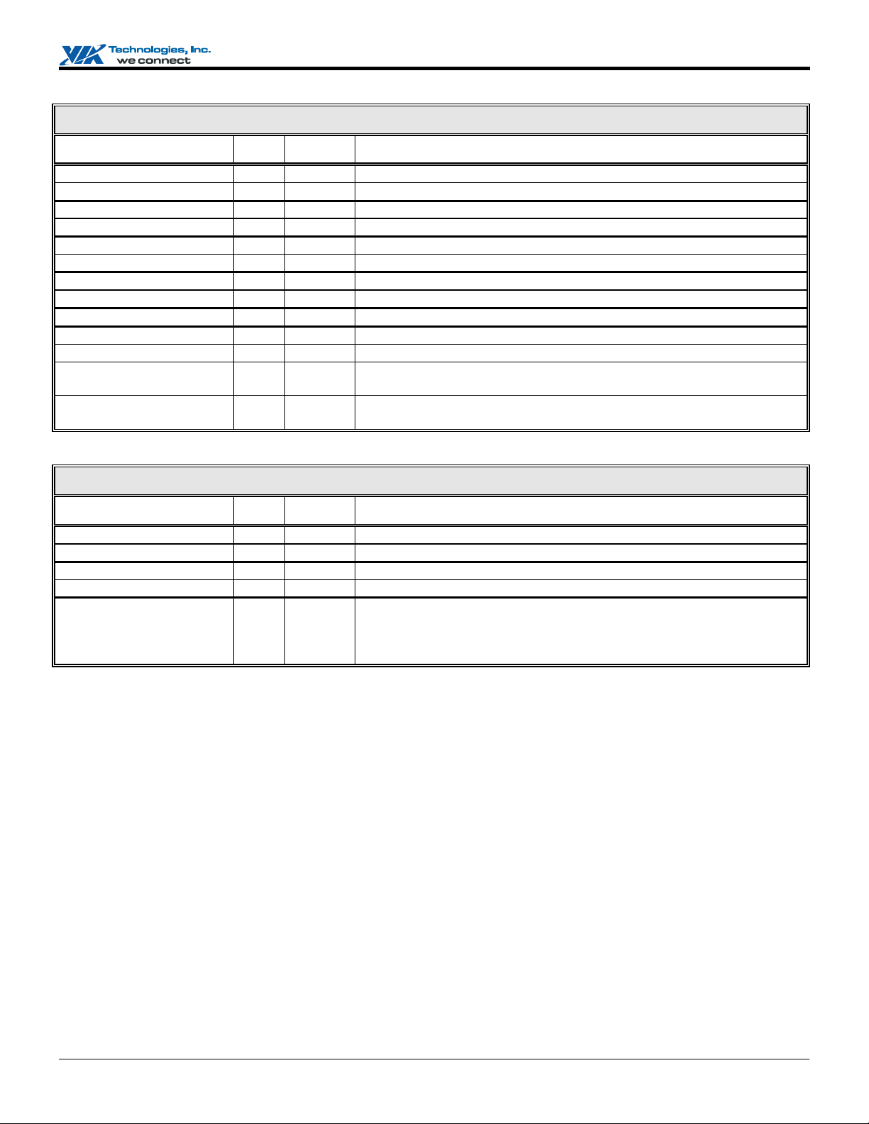
PREQH#
PGNTH#
PREQL#
PGNTL#
HREQ1# / GPI10 Y11 I / IO High Priority Request 1. Device 0 Function 4 RxE5[3] = 1.
HGNT1# / GPO8 W11 O / IO High Priority Grant 1. Device 0 Function 4 RxE5[3] = 1.
HREQ2# / GPI11 V11 I / IO High Priority Request 2. Device 0 Function 4 RxE5[3] = 1.
HGNT2# / GPO9 T10 O / IO High Priority Grant 2. Device 0 Function 4 RxE5[3] = 1.
LREQ1# / GPI12 U10 I / IO Low Priority Request 1. Device 0 Function 4 RxE5[2] = 1.
LGNT1# / GPO10 Y10 O / IO Low Priority Grant 1. Device 0 Function 4 RxE5[2] = 1.
LREQ2# / GPI13 / IOCHRDY W10 I / IO Low Priority Request 2. Device 0 Func 4 RxE5[2]=1, Func 0 Rx67[3]=0
LGNT2# / GPO11 V10 O / IO Low Priority Grant 2. Device 0 Function 4 RxE5[2] = 1.
PCI Slot
PCI Slot
PCI Slot
PCI Slot
C1 O PCI Request. This signal goes to the North Bridge REQ4# input to
request the PCI bus for high priority access. The internal LAN requests the
PCI bus using this signal, so if the LAN subsystem is used, this signal must
be connected (one of the H/LREQ/GNT 1 and 2 pairs provided by the
VT8231 may be used to implement the fifth PCI slot if desired). If the
LAN subsystem is not used, PREQH# / PGNTH# may optionally remain
unconnected.
D3 I PCI Grant. This signal is driven by the North Bridge GNT4# signal to
grant high priority PCI access to the VT8231.
D2 O PCI Request. This signal goes to the North Bridge PREQ# input to
request the PCI bus for normal priority access.
D1 I PCI Grant. This signal is driven by the North Bridge PGNT# output to
grant normal priority PCI access to the VT8231.
REQ/GNT 3
REQ/GNT 2
REQ/GNT 1
REQ/GNT 0
PCI Slot
PCI Slot
On-Board
High Priority
PCI Master
On-Board
High Priority
PCI Master
H REQ/GNT 1
H REQ/GNT 2
L REQ/GNT 1
L REQ/GNT 2
VIA
North Bridge
VT8231
South Bridge
REQ/GNT 4
PREQ/GNT
PREQ/GNT L
PREQ/GNT H
Figure 5. PCI Request / Grant Connections Using the VT8231
Revision 2.32, September 1, 2004 -11- Pin Descriptions
Page 18

VT8231 South Bridge
CPU Interface
Signal Name Pin # I/O Signal Description
CPURST
INTR
NMI
INIT#
STPCLK#
SMI#
FERR#
IGNNE#
SLP# / GPO7 U6 OD Sleep (F4 RxE4[4] = 1). Used to put the CPU to sleep. Used with slot-1
A20M#
DTD+
DTD-
Note: Connect each of the above signals to 4.7K Ω pullup resistors to VCC3.
U4 OD CPU Reset. The VT8231 asserts CPURST to reset the CPU during power-up.
R6 OD CPU Interrupt. INTR is driven by the VT8231 to signal the CPU that an
interrupt request is pending and needs service.
T5 OD Non-Maskable Interrupt. NMI is used to force a non-maskable interrupt to
the CPU. The VT8231 generates an NMI when SERR# is asserted.
V5 OD Initialization. The VT8231 asserts INIT# if it detects a shut-down special
cycle on the PCI bus or if a soft reset is initiated by the register. See strap on
SUSA# / GPO1 for polarity selection.
V6 OD Stop Clock. STPCLK# is asserted by the VT8231 to the CPU to throttle the
processor clock.
Y5 OD System Management Interrupt. SMI# is asserted by the VT8231 to the CPU
in response to different Power-Management events.
U5 I Numerical Coprocessor Error. This signal is tied to the coprocessor error
signal on the CPU. Internally generates interrupt 13 if active. A threshold of
1.5V or 2.5V is selectable via Device 0 Function 0 Rx67[2].
T6 OD Ignore Numeric Error. This pin is connected to the “ignore error” pin on the
CPU.
CPUs only. Not currently used with socket-7 CPUs.
W5 OD A20 Mask. Connect to A20 mask input of the CPU to control address bit-20
generation. Logical combination of the A20GATE input (from internal or
external keyboard controller) and Port 92 bit-1 (Fast A20). See Device 0
Function 0 Rx59[1].
L2 Analog I CPU DTD (Thermal Diode) Channel Plus. Connect to cathode of first
external temperature sensing diode.
L3 Analog I CPU DTD (Thermal Diode) Channel Minus. Connect to anode of first
external temperature sensing diode.
Revision 2.32, September 1, 2004 -12- Pin Descriptions
Page 19
VT8231 South Bridge
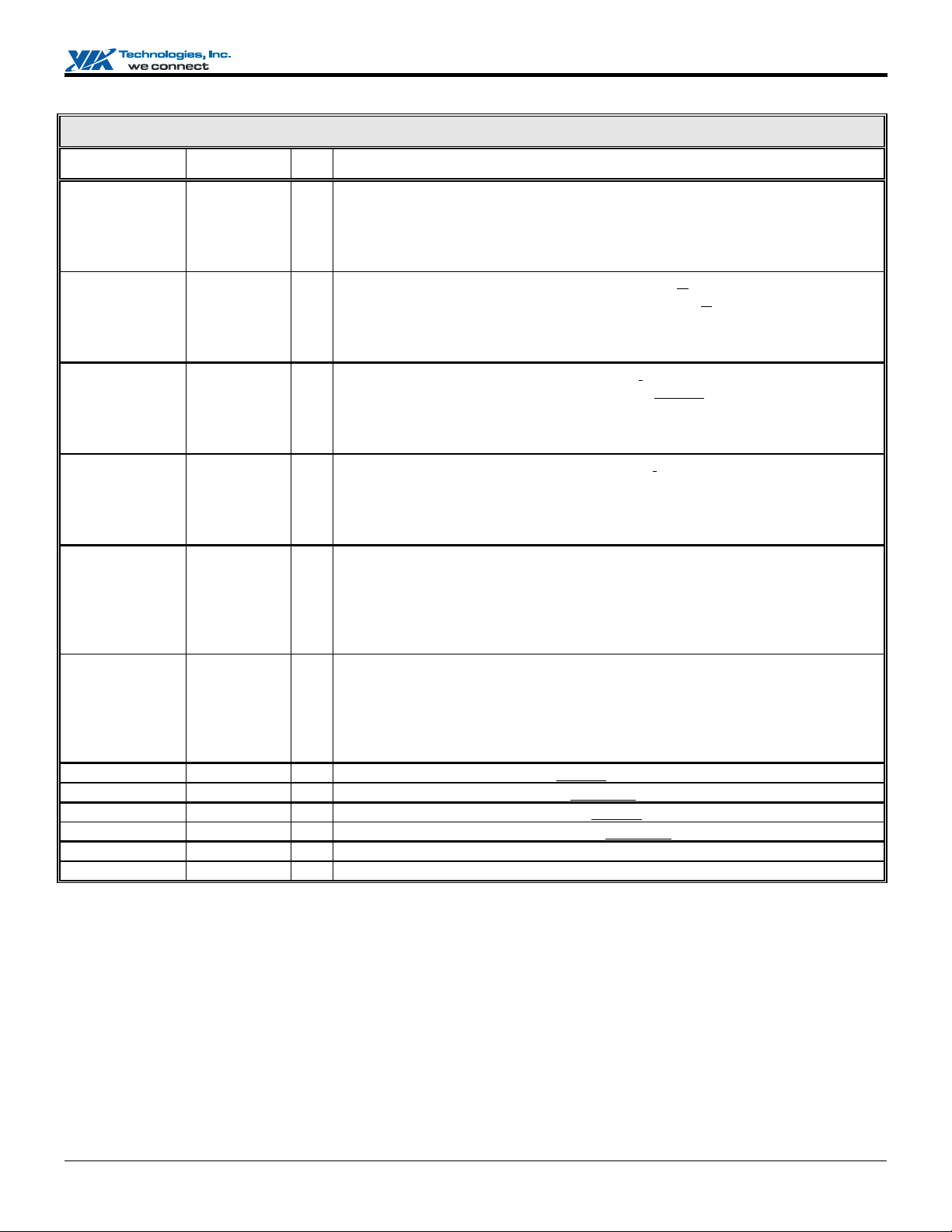
Strap Options
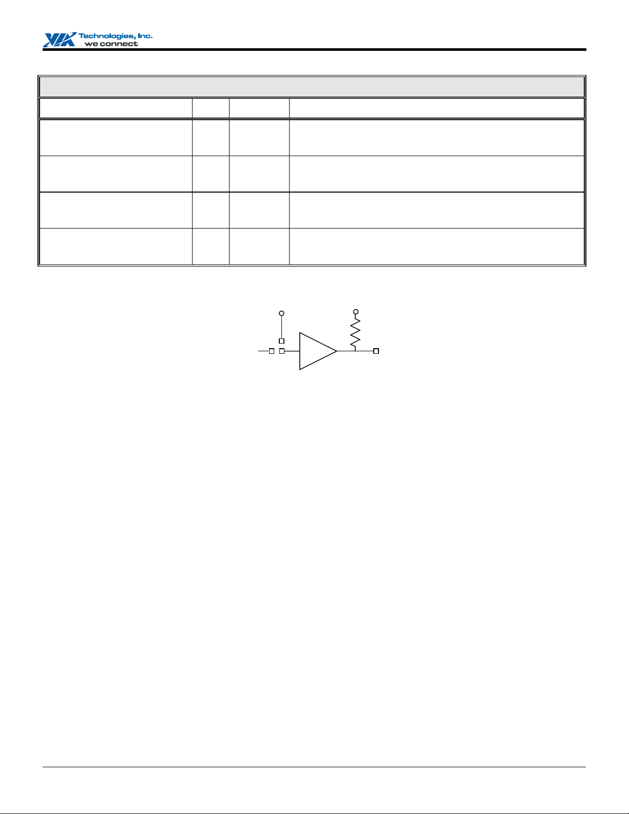
Signal Name Pin # I/O Signal Description
Strap / SUSA# / GPO1 P1 I / O
CPURST / INIT# Polarity
H: Slot-1 / Socket-370 / Slot-A / Socket-A
L: Socket-7
Strap / MCCS# / GPO17 W6 I / O
CPU Frequency Strapping
H: Disable
L: Enable
Strap / SA16 Y14 I / IO
BIOS ROM Interface
H: LPC
L: Conventional
Strap / SA17 T13 I / IO
Auto Reboot
H: Disable (recommended)
L: Enable
Note: External strap option values may be set by connecting the indicated external pin to a 4.7K ohm pullup (for 1 or H) or
driving it low during reset with a 7407 TTL open collector buffer (for 0 or L) as shown in the suggested circuit below:
VCC
7407
RESET#
VCC
4.7K
strap
pin
Figure 6. Strap Option Circuit
Revision 2.32, September 1, 2004 -13- Pin Descriptions
Page 20
VT8231 South Bridge
Advanced Programmable Interrupt Controller (APIC) Interface
Signal Name Pin # I/O Signal Description
WSC# / GPI14 V4 I / I Internal APIC Write Snoop Complete. F0 Rx58[6] = 1.
Asserted by the north bridge to indicate that all snoop activity
on the CPU bus initiated by the last PCI-to-DRAM write is
complete and that it is safe to perform an APIC interrupt.
APICD0 / GPO28 W4 O / O Internal APIC Data 0. F0 Rx58[6] = 1.
APICD1 / GPO29 Y4 O / O Internal APIC Data 1. F0 Rx58[6] = 1.
APICCLK / GPI9 Y3 I / I APIC Clock. F0 Rx58[6] = 1.
Low Pin Count (LPC) Interface
Signal Name Pin # I/O Signal Description
LFRAME#
LDRQ# / GPI15 Y8 I / I LPC Data Request. F0 Rx58[5] = 1 and F4 RxE5[7] = 0.
LAD[3-0]
Note: For LPC control, see Device 0 Function 0 Rx58[5] and Rx59[4-3]
Note: Connect the LPC interface LPCRST# (LPC Reset) signal to PCIRST#
W8 O
V7, W7, Y7, V8 IO
LPC Frame.
LPC Address / Data.
Revision 2.32, September 1, 2004 -14- Pin Descriptions
Page 21
VT8231 South Bridge
LAN Controller - Media Independent Interface (MII)
Signal Name Pin # I/O Signal Description
MCOL
MCRS
MDCK
MDIO
MRXCLK
MRXD[3],
MRXD[2],
MRXD[1],
MRXD[0]
MRXDV
MRXERR
MTXCLK
MTXD[3],
MTXD[2],
MTXD[1],
MTXD[0]
MTXENA
The internal LAN controller uses the high priority PCI bus request / grant pair (PREQH# / PGNTH#) to request PCI bus access
from the chipset north bridge.
G17 I MII Collision Detect. From the external PHY.
G16 I MII Carrier Sense. Asserted by the external PHY when the media is active.
C20 O MII Management Data Clock. Sent to the external PHY as a timing reference for MDIO
D18 IO MII Management Data I/O. Read from the MDI bit or written to the MDO bit.
C19 I MII Receive Clock. 2.5 or 25 MHz clock recovered by the PHY.
D19
D20
E18
E19
E20 I
F18 I MII Receive Error. Asserted by the PHY when it detects a data decoding error.
F17 I MII Transmit Clock. Always active 2.5 or 25 MHz clock supplied by the PHY.
G20
G19
G18
F20
F19 O MII Transmit Enable. Indicates transmit active from the MII port to the PHY.
I
MII Receive Data. Parallel receive data lines driven by the external PHY synchronous with
I
MRXCLK.
I
I
MII Receive Data Valid.
O
MII Transmit Data. Parallel transmit data lines synchronized to MTXCLK.
O
O
O
Serial EEPROM Interface
Signal Name Pin # I/O Signal Description
EECS#
EECK
EEDO
EEDI
C18 O
E16 O
D17 I Serial EEPROM Data Output. Connect to EEPROM Data Out pin.
E17 O Serial EEPROM Data Input. Connect to EEPROM Data In pin.
Serial EEPROM Chip Select.
Serial EEPROM Clock.
Revision 2.32, September 1, 2004 -15- Pin Descriptions
Page 22
VT8231 South Bridge
Universal Serial Bus Interface
Signal Name Pin # I/O Signal Description
USBP0+
USBP0USBP1+
USBP1USBP2+
USBP2USBP3+
USBP3USBCLK
USBOC0#
USBOC1#
USBOC2# / LA20
/ GPI20 / GPO20
USBOC3# / LA21
/ GPI21 / GPO21
For USB interface configuration and control see also Functions 2 and 3 plus Function 0 Rx48[3-2], 4A[1], 4D[1-0], 50[5-4]
B18 IO
A18 IO
B19 IO
A19 IO
B20 IO
A20 IO
C17 IO
B17 IO
C15 I USB Clock. 48MHz clock input for the USB interface
A17 I USB Port 0 Over Current Detect. Port 0 is disabled if this input is low.
D16 I USB Port 1 Over Current Detect. Port 1 is disabled if this input is low
W13 I / IO
/ I / O
Y13 I / IO
/ I / O
USB Port 0 Data +
USB Port 0 Data USB Port 1 Data +
USB Port 1 Data USB Port 2 Data +
USB Port 2 Data USB Port 3 Data +
USB Port 3 Data -
USB Port 2 Over Current Detect. Port 2 is disabled if this input is low.
Device 0 Function 4 RxE4[6] = 0 and Power Management I/O Rx4E[4] = 1
USB Port 3 Over Current Detect. Port 3 is disabled if this input is low.
Device 0 Function 4 RxE4[6] = 0 and Power Management I/O Rx4E[5] = 1
System Management Bus (SMB) Interface (I2C Bus)
Signal Name Pin # I/O Signal Description
SMBCK1
SMBCK2 / GPIO27 R1 IO / IO SMB / I2C Channel 2 Clock†. F4 Rx55[3] = 0.
SMBDT1
SMBDT2 / GPIO26 R2 IO / IO SMB / I2C Channel 2 Data†. F4 Rx55[3] = 0.
SMBALRT# / GPI7 T2 I / I SMB Alert. (System Management Bus I/O space Rx08[3] = 1) When the
For SMB interface configuration and control see also Function 4 Rx54[7], 55[3-2], 56[4], 90-93, D2-D6 plus SMB I/O Rx0-F,
HWM I/O Rx48, and PMIO Rx45[1-0]
† Note: SMBus #2 is a slave-only device used to supply status for external Alert-On-LAN (AOL)
R3 IO
T1 IO
SMB / I2C Channel 1 Clock.
SMB / I2C Channel 1 Data.
chip is enabled to allow it, assertion generates an IRQ or SMI interrupt or a
power management resume event. The same pin is used as General Purpose
Input 6 whose value is reflected in Rx48[6] of function 4 I/O space
Revision 2.32, September 1, 2004 -16- Pin Descriptions
Page 23
VT8231 South Bridge
UltraDMA-33 / 66 / 100 Enhanced IDE Interface
Signal Name Pin # I/O Signal Description
PDRDY /
PDDMARDY /
PDSTROBE
SDRDY /
SDDMARDY /
SDSTROBE
PDIOR# /
PHDMARDY /
PHSTROBE
SDIOR# /
SHDMARDY /
SHSTROBE
PDIOW# /
PSTOP
SDIOW# /
SSTOP
PDDRQ
SDDRQ
PDDACK#
SDDACK#
IRQ14
IRQ15
N19 I EIDE Mode: Primary I/O Channel Ready. Device ready indicator
UltraDMA Mode: Primary Device DMA Ready. Output flow control. The device
may assert DDMARDY to pause output transfers
Primary Device Strobe. Input data strobe (both edges). The
device may stop DSTROBE to pause input data transfers
Y20 I EIDE Mode: Secondary I/O Channel Ready. Device ready indicator
UltraDMA Mode: Secondary Device DMA Ready. O
device may assert DDMARDY to pause output transfers
Secondary Device Strobe. Input data strobe (both edges). The
device may stop DSTROBE to pause input data transfers
N18 O EIDE Mode: Primary Device I/O Read. Device read strobe
UltraDMA Mode: Primary Host DMA Ready. Primary
The host may assert HDMARDY to pause input transfers
Primary Host Strobe. Output data strobe (both edges). The host
may stop HSTROBE to pause output data transfers
W19 O EIDE Mode: Secondary Device I/O Read. Device read strobe
UltraDMA Mode: Secondary Host DMA Ready. Input flow control. The host may
assert HDMARDY to pause input transfers
Host Strobe B. Output strobe (both edges). The host may stop
HSTROBE to pause output data transfers
P20 O EIDE Mode: Primary Device I/O Write. Device write strobe
UltraDMA Mode: Primary Stop. Stop transfer: Asserted by the host prior to
initiation of an UltraDMA burst; negated by the host before data
is transferred in an UltraDMA burst. Assertion of STOP by the
host during or after data transfer in UltraDMA mode signals the
termination of the burst.
Y19 O EIDE Mode: Secondary Device I/O Write. Device write strobe
UltraDMA Mode: Secondary Stop. Stop transfer: Asserted by the host prior to
initiation of an UltraDMA burst; negated by the host before data
is transferred in an UltraDMA burst. Assertion of STOP by the
host during or after data transfer in UltraDMA mode signals the
termination of the burst.
P19 I Primary Device DMA Request. Primary
U17 I Secondary Device DMA Request. Secondary
N20 O Primary Device DMA Acknowledge. Primary
W20 O Secondary Device DMA Acknowledge. Secondary
T14 I
U14 I
Primary Channel Interrupt Request.
Secondary Channel Interrupt Request.
channel DMA request
channel DMA request
channel DMA acknowledge
utput flow control. The
channel input flow control.
channel DMA acknowledge
Revision 2.32, September 1, 2004 -17- Pin Descriptions
Page 24

VT8231 South Bridge
UltraDMA-33 / 66 / 100 Enhanced IDE Interface (continued)
Signal Name Pin # I/O Signal Description
PDCS1#
PDCS3#
SDCS1#
SDCS3#
PDA[2-0]
SDA[2-0]
PDD[15-0]
SDD[15-0] / SA[15-0] W18, V17, Y17, W16,
For IDE / UDMA interface configuration and control see also Function 1 plus Function 0 Rx48[1-0], 4A[0], 4C, 50[3] 7C[5-4]
T17, R17, T18, T20,
P17, N16, R19, P18,
R18, R20, N17, P16,
T19, U20, R16, T16
V15, Y15, W14, T15,
U15, U16, V14, W15,
Y16, V16, W17, Y18
L18 O Primary Master Chip Select. This signal corresponds to CS1FX#
on the primary IDE connector.
L19 O Primary Slave Chip Select. This signal corresponds to CS3FX# on
the primary IDE connector.
U18 O Secondary Master Chip Select. This signal corresponds to
CS17X# on the secondary IDE connector.
U19 O Secondary Slave Chip Select. This signal corresponds to CS37X#
on the secondary IDE connector.
M20, M18, M19 O Primary Disk Address. PDA[2:0] are used to indicate which byte
in either the ATA command block or control block is being
accessed.
V20, V18, V19 O Secondary Disk Address. SDA[2:0] are used to indicate which
byte in either the ATA command block or control block is being
accessed.
IO
Primary Disk Data
IO
Secondary Disk Data / ISA Address
Revision 2.32, September 1, 2004 -18- Pin Descriptions
Page 25
VT8231 South Bridge
MIDI Interface
Signal Name Pin # I/O Signal Description
MSI
MSO
For MIDI interface configuration and control see also SuperIO RxF9[0], Function 0 Rx6D[2-0], Function 4 Rx40[0], Function 5
Rx18 and I/O Base 2 Rx0, and Function 5/6 Rx42[7,6,1], 43[3-2]
G4 I
J4 O
MIDI Serial In
MIDI Serial Out
AC97 Audio / Modem Interface
Signal Name Pin # I/O Signal Description
ACRST#
ACSYNC
ACSDOUT
ACSDIN0
ACSDIN1
ACSDIN2 / GPIO19 G5 I AC97 Serial Data In 2. Function 4, RxE4[5] = 0
ACSDIN3 / GPI15 / LDRQ# Y8 I AC97 Serial Data In 3. Function 4, RxE5[7] = 1
ACBITCLK
For AC97 interface configuration and control see also Functions 5 and 6 plus Function 0 Rx4D[3-2], 50[7-6], PMIO Rx20[13].
G2 O
G1 O
H3 O
H1 I
H2 I
J3 I
AC97 Reset
AC97 Sync
AC97 Serial Data Out
AC97 Serial Data In 0
AC97 Serial Data In 1
AC97 Bit Clock
Game Port Interface
Signal Name Pin # I/O Signal Description
JAX
JAY
JBX
JBY
JAB1 / GPI28 G3 I / I
JAB2 / GPO12 H5 I / O Joystick A Button 2. Device 0 Function 4 RxE5[4] = 1.
JBB1 / GPI29 F1 I / I
JBB2 / GPO13 H4 I / O Joystick B Button 2. Device 0 Function 4 RxE5[4] = 1.
For Game Port interface configuration and control see also Game Port I/O registers (port 201h), Function 0 Rx6D[3], Function 4
Rx40[2], and Function 5/6 Rx42[3] and 4A
J1 I
K4 I
K5 I
J2 I
Joystick A X-axis
Joystick A Y-axis
Joystick B X-axis
Joystick B Y-axis
Joystick A Button 1.
Joystick B Button 1.
Revision 2.32, September 1, 2004 -19- Pin Descriptions
Page 26
VT8231 South Bridge
Floppy Disk Interface
Signal Name Pin # I/O Signal Description
DRVDEN0
DRVDEN1
MTR0#
MTR1#
DS0#
DS1#
DIR#
STEP#
INDEX#
HDSEL#
TRK00#
RDATA#
WDATA#
WGATE#
DSKCHG#
WRTPRT#
See also Parallel Port pin descriptions for optional Floppy Disk interface functionality
L17 O
K17 O
K18 O Motor Control 0. Select motor on drive 0.
J16 O Motor Control 1. Select motor on drive 1
J17 O Drive Select 0. Select drive 0.
K19 O Drive Select 1. Select drive 1
K20 O Direction. Direction of head movement (0 = inward motion, 1 = outward motion)
J18 O Step. Low pulse for each track-to-track movement of the head.
L20 I Index. Sense to detect that the head is positioned over the beginning of a track
H19 O Head Select. Selects the side for R/W operations (0 = side 1, 1 = side 0)
H16 I Track 0. Sense to detect that the head is positioned over track 0.
H20 I Read Data. Raw serial bit stream from the drive for read operatrions.
J19 O Write Data. Encoded data to the drive for write operations.
J20 O Write Gate. Signal to the drive to enable current flow in the write head.
H18 I Disk Change. Sense that the drive door is open or the diskette has been changed
H17 I Write Protect. Sense for detection that the diskette is write protected (causes write
Drive Density Select 0.
Drive Density Select 1.
since the last drive selection.
commands to be ignored)
Revision 2.32, September 1, 2004 -20- Pin Descriptions
Page 27
VT8231 South Bridge
Parallel Port Interface
Signal Name Pin # I/O Signal Description
PINIT# / DIR# B12 IO / O Initialize. Initialize printer. Output in standard mode, I/O in ECP/EPP mode.
STROBE# / nc A11 IO / - Strobe. Output used to strobe data into the printer. I/O in ECP/EPP mode.
AUTOFD# / DRVEN0 E11 IO / O Auto Feed. Output used to cause the printer to automatically feed one line after
each line is printed. I/O pin in ECP/EPP mode.
SLCTIN# / STEP# D12 IO / O Select In. Output used to select the printer. I/O pin in ECP/EPP mode.
SLCT / WGATE# E13 I / O Select. Status output from the printer. High indicates that it is powered on.
ACK# / DS1# B14 I / O Acknowledge. Status output from the printer. Low indicates that it has received
the data and is ready to accept new data
ERROR# / HDSEL# F11 I / O Error. Status output from the printer. Low indicates an error condition in the
printer.
BUSY / MTR1# A14 I / O Busy. Status output from the printer. High indicates not ready to accept data.
PE / WDATA# D13 I / O Paper End. Status output from the printer. High indicates that it is out of paper.
PD7 / nc,
PD6 / nc,
PD5 / nc,
PD4 / DSKCHG#,
PD3 / RDATA#,
PD2 / WRTPRT#,
PD1 / TRK00#,
PD0 / INDEX#
As shown by the alternate functions above, in mobile applications the parallel port pins can optionally be selected to function as a
floppy disk interface for attachment of an external floppy drive using the parallel port connector (see Super I/O Configuration
Index F6[5]).
C14
A13
B13
C13
E12
A12
C12
D11
IO / IO / IO / IO / I
IO / I
IO / I
IO / I
IO / I
Parallel Port Data.
Revision 2.32, September 1, 2004 -21- Pin Descriptions
Page 28
VT8231 South Bridge
Serial Port and Infrared Interface
Signal Name Pin # I/O Signal Description
TXD
RXD
IRTX / GPO14 R8 O / O Infrared Transmit. IR transmit data out (Function 4 RxE5[5] = 0).
IRRX / GPO15 U8 I / O Infrared Receive. IR receive data in (Function 4 RxE5[5] = 0).
IRRX2 / GPIOB T8 I Infrared Receive. IR receive data in (see FIR I/O Rx33 and 34)
RTS#
CTS#
DTR#
DSR#
DCD#
RI#
B15 O Transmit Data. Serial port transmit data out.
E14 I Receive Data. Serial port receive data in.
A15 O Request To Send. Indicator that the serial output port is ready to transmit data.
Typically used as hardware handshake with CTS# for low level flow control.
Designed for direct input to external RS-232C driver.
B16 I Clear To Send. Indicator to the serial port that an external communications
device is ready to receive data. Typically used as hardware handshake with RTS#
for low level flow control. Designed for input from external RS-232C receiver.
A16 O Data Terminal Ready. Indicator that serial port is powered, initialized, and
ready. Typically used as hardware handshake with DSR# for overall readiness to
communicate. Designed for direct input to external RS-232C driver.
D14 I Data Set Ready. Indicator to serial port that an external serial communications
device is powered, initialized, and ready. Typically used as hardware handshake
with DTR# for overall readiness to communicate. Designed for direct input from
external RS-232C receiver.
D15 I Data Carrier Detect. Indicator to serial port that an external modem is detecting
a carrier signal (i.e., a communications channel is currently open). In direct
connect environments, this input will typically be driven by DTR# as part of the
DTR/DSR handshake. Designed for direct input from external RS-232C receiver.
C16 I Ring Indicator. Indicator to serial port that an external modem is detecting a ring
condition. Used by software to initiate operations to answer and open the
communications channel. Designed for direct input from external RS-232C
receiver (whose input is typically not connected in direct connect environments).
Revision 2.32, September 1, 2004 -22- Pin Descriptions
Page 29
VT8231 South Bridge
Conventional BIOS ROM / ISA Bus Interface
Signal Name Pin # I/O Signal Description
LA21 / USBOC3#
/ GPI21 / GPO21
LA20 / USBOC2#
/ GPI20 / GPO20
SA[19:18],
SA17 / strap,
SA16 / strap,
SA[15:0] / SDD[15:0]
SD[7-0]
IOR# / GPI22 / GPO22 U7 IO I/O Read (Function 4 RxE4[7] = 1.). Command to ISA I/O
IOW# / GPI23 / GPO23 T7 IO I/O Write (Function 4 RxE4[7] = 1.). Command to ISA I/O
MEMR#
MEMW#
IOCHRDY / LREQ2# / GPI13 W10 I I/O Channel Ready (Function 0 Rx67[3] = 1). Normally
IRQ1 / MSCK N2 I
IRQ8# / GPI1 V3 I Interrupt 8 (optional external RTC). Enabled if Rx51[3]
IRQ12 / MSDT N4 I
IRQ14
IRQ15
SPKR
W18, V17, Y17, W16,
V15, Y15, W14, T15,
U15, U16, V14, W15,
Y16, V16, W17, Y18
T11, R11, U11, U12,
Y12, W12, V12, R12
Y13
W13
V13, U13,
T13,
Y14,
W9 IO Memory Read. Command to memory slave to indicate that
Y9 IO Memory Write. Command to memory slave to indicate that
T14 I
U14 I
U9 O Speaker Drive. Output of internal timer/counter 2.
O
System Address Bus. Allows access to physical memory
devices (e.g., BIOS ROMs) up to 4 Mbytes. F4 RxE4[6] =
O
1.
IO System Address Bus. These address lines are used to
interface to BIOS ROMs but may also be used to implement
a subset of the ISA bus if required. SA[19-16] are connected
to ISA bus SA[19-16] directly. SA[19-17] are also
connected to LA[19-17] of the ISA bus.
SA17 strap – 0/1 = Enable / Disable Auto Reboot
SA16 strap – 0/1 = Disable / Enable LPC ROM
IO System Data. SD[7:0] provide the data path for BIOS
ROMs and other 8-bit devices residing on the ISA bus.
slave devices to indicate that the slave may drive data on to
the ISA data bus.
slave devices to indicate that the slave may latch data from
the ISA data bus.
it may drive data onto the ISA data bus.
it may latch data from the ISA data bus.
pulled high on the motherboard. Devices on the ISA Bus
assert IOCHRDY low to indicate that additional time (wait
states) is required to complete the cycle.
Interrupt 1 (optional external Keyboard Controller).
= 0.
Interrupt 12 (optional external PS2 Mouse Controller).
Interrupt 14 (IDE Primary Channel).
Interrupt 15 (IDE Secondary Channel).
Serial IRQ
Signal Name Pin # I/O Signal Description
SERIRQ
Revision 2.32, September 1, 2004 -23- Pin Descriptions
V9 I
Serial IRQ.
Page 30
VT8231 South Bridge
Internal Keyboard Controller
Signal Name Pin # I/O Signal Description
MSCK / IRQ1 N2 IO / I MultiFunction Pin (Internal mouse controller enabled by F0 Rx51[2])
Rx51[2]=1 Mouse Clock. From internal mouse controller.
Rx51[2]=0 Interrupt Request 1. Interrupt 1 (external KBC).
MSDT / IRQ12 N4 IO / I MultiFunction Pin (Internal mouse controller enabled by F0 Rx51[2])
Rx51[2]=1 Mouse Data. From internal mouse controller.
Rx51[2]=0 Interrupt Request 12. Interrupt 12 (ext PS2 mouse ctlr).
KBCK / A20GATE M4 IO / I MultiFunction Pin (Internal keyboard controller enabled by F0 Rx51[0])
Rx51[0]=1 Keyboard Clock. From internal keyboard controller
Rx51[0]=0 Gate A20. Input from external keyboard controller.
KBDT / KBRC N1 IO / I MultiFunction Pin (Internal keyboard controller enabled by F0 Rx51[0])
Rx51[0]=1 Keyboard Data. From internal keyboard controller.
Rx51[0]=0 Keyboard Reset. From external keyboard controller (KBC)
for CPURST# generation
KBCS# / ROMCS# T9 O / O Keyboard Chip Select (Rx51[0]=0). To external keyboard controller chip.
For Keyboard Controller configuration and control see also I/O Ports 60h and 64h, Configuration Index ports 3F0h and 3F1h (and
configuration registers at offsets E0-E6h) plus Function 0 Rx51[2-0] and PMIO Rx20[2], 30[9], 34[9], and 38[7].
Chip Selects
Signal Name Pin # I/O Signal Description
ROMCS# / KBCS# T9 O / O ROM Chip Select (Rx51[0]=1). Chip Select to the BIOS ROM. See also
Device 0 Rx40[5-4] and Rx41.
MCCS# / GPO17 / strap W6 O / IO Microcontroller Chip Select (Device 0 Function 4 RxE4[3] = 0). Asserted
during read or write accesses to I/O ports 62h or 66h.
Strap: 0/1 = Enable / Disable CPU Frequency Strapping
PCS# / GPO16 Y6 O / IO / IO Programmable Chip Select. (Device 0 Function 4 RxE4[2] = 0). Asserted
during I/O cycles to programmable read or write ISA I/O port ranges.
Revision 2.32, September 1, 2004 -24- Pin Descriptions
Page 31

VT8231 South Bridge
General Purpose Inputs
Signal Name Pin # I/O Signal Description
GPI0 [VBAT]
GPI1 / IRQ8# [VCCSUS] V3 I General Purpose Input 1. F0 Rx51[3] = 1.
GPI2 / EXTSMI# [VCCSUS] W1 I / IO General Purpose Input 2. (Use as GPI -or- as EXTSMI#)
GPI3 / RING# [VCCSUS] U3 I / I General Purpose Input 3. (Use as GPI -or- as RING#)
GPI4 / LID [VCCSUS] V2 I / I General Purpose Input 4. (Use as GPI -or- as LID)
GPI5 / BATLOW# [VCCSUS] T3 I / I General Purpose Input 5. (Use as GPI -or- as BATLOW#)
GPI6 / PME# [VCCSUS] U1 I / I General Purpose Input 6. (Use as GPI -or- as PME#)
GPI7 / SMBALRT# [VCCSUS] T2 I / I General Purpose Input 7. (Use as GPI -or- as SMBALRT#)
GPI8 / INTRUDER# [VBAT] F3 I / I General Purpose Input 8. (Use as GPI -or- as INTRUDER#)
GPI9 / APICCLK Y3 I / I General Purpose Input 9. Rx58[6]=0
GPI10 / HREQ1# Y11 I / I General Purpose Input 10. F4 RxE5[3]=1
GPI11 / HREQ2# V11 I / I General Purpose Input 11. F4 RxE5[3]=1
GPI12 / LREQ1# U10 I / I General Purpose Input 12. F4 RxE5[2]=1
GPI13 / LREQ2# / IOCHRDY W10 I / I / I General Purpose Input 13. F4 RxE5[2]=1, F0 Rx67[3]=0
GPI14 / WSC# V4 I / I General Purpose Input 14. Rx58[6]=0
GPI15 / LDRQ# / ACSDIN3 Y8 I / I / I General Purpose Input 15. Rx58[5]=0 & F4 RxE5[7]=0
GPI16 / CPUMISS V1 I / I General Purpose Input 16. (Use as GPI -or- as CPUMISS)
GPI17 / AOLGPI / THRM P3 I / I / I General Purpose Input 17. F4 Rx40[7]=0
GPI18 / GPO18 / FAN2 / SLPBTN# K3 I / O / I / I General Purpose Input 18. F4 RxE5[0]=0
GPI19 / GPO19 / ACSDIN2 G5 I / O / I General Purpose Input 19. F4 RxE5[1]=0 & E4[5]=0
GPI20 / GPO20 / LA20 / USBOC2# W13 I / OD / IO / I General Purpose Input 20. F4 RxE4[6]=0 & PMIO 4E[4]=1
GPI21 / GPO21 / LA21 / USBOC3# Y13 I / OD / IO / I General Purpose Input 21. F4 RxE4[6]=0 & PMIO 4E[5]=1
GPI22 / GPO22 / IOR# U7 I / OD / IO General Purpose Input 22. F4 RxE4[7]=0 & PMIO 4E[6]=1
GPI23 / GPO23 / IOW# T7 I / OD / IO General Purpose Input 23. F4 RxE4[7]=0 & PMIO 4E[7]=1
GPI24 / GPO24 / GPIOA Y2 I / OD / IO General Purpose Input 24. F4 RxE6[0]=0
GPI25 / GPO25 / GPIOC
/ CHSINOUT
GPI26 / GPO26 / SMBDT2 [VCCSUS] R2 I / OD / IO General Purpose Input 26. F4 Rx55[2]=1 & 55[3]=0
GPI27 / GPO27 / SMBCK2 [VCCSUS] R1 I / OD / IO General Purpose Input 27. F4 Rx55[2]=1 & 55[3]=0
GPI28 / JAB1 G3 I / I General Purpose Input 28. (Use as GPI -or- as JAB1)
GPI29 / JBB1 F1 I / I General Purpose Input 29. (Use as GPI -or- as JBB1)
GPI30 / GPO30 / GPIOD Y1 I / OD / IO General Purpose Input 30. F4 RxE6[6]=0
GPI31 / GPO31 / GPIOE W3 I / OD / IO General Purpose Input 31. F4 RxE6[7]=0
Note: See also Power Management I/O Registers Rx50 and 52 for GPI pin status and SCI/SMI select.
Note. The state of each GPI pin may be read at the corresponding bit of PMIO Rx4B-48.
Note: Each of the pins above may be used as a GPI pin or as one of the alternate functions listed above for that pin. Descriptions
of these alternate functions are given elsewhere in the pin descriptions section of this document. If a control bit must be set to
enable / select each of the above pins for use as a General Purpose Input, the bit setting is listed above. If no bit setting is listed,
either function may be used (no bit setting is required to select the GPI function), however note that typical designs may use the
pin as one or the other (but not both GPI and alternate function at the same time).
F4 I
J5 I / OD / IO
/ IO
General Purpose Input 0.
General Purpose Input 25. F4 RxE6[1]=0 & E5[6]=0
(F4 RxE5[6]=1 to enable CHSINOUT function on this pin)
Revision 2.32, September 1, 2004 -25- Pin Descriptions
Page 32

VT8231 South Bridge
General Purpose Outputs
Signal Name Pin # I/O Signal Description
GPO0 / SLOWCLK [VCCSUS] R4 O / O General Purpose Output 0. (Func 4 Rx54[1-0] = 00).
Output value determined by PMU I/O Rx4C[0]
GPO1 / SUSA# / strap [VCCSUS] P1 O / O / I General Purpose Output 1. F4 Rx54[2]=1
GPO2 / SUSB# [VCCSUS] P2 O / O General Purpose Output 2. F4 Rx54[3]=1
GPO3 / SUSST1# [VCCSUS] N5 O / O General Purpose Output 3. F4 Rx54[4]=1
GPO4 / SUSCLK [VCCSUS] W2 O / O General Purpose Output 4. F4 Rx55[1]=1
GPO5 / CPUSTP# P4 O / O General Purpose Output 5. F4 RxE4[0]=1
GPO6 / PCISTP# T4 O / O General Purpose Output 6. F4 RxE4[1]=1
GPO7 / SLP# U6 O / O General Purpose Output 7. F4 RxE4[4]=1
GPO8 / HGNT1# W11 O / O General Purpose Output 8. F4 RxE5[3]=1
GPO9 / HGNT2# T10 O / O General Purpose Output 9. F4 RxE5[3]=1
GPO10 / LGNT1# Y10 O / O General Purpose Output 10. F4 RxE5[2]=1
GPO11 / LGNT2# V10 O / O General Purpose Output 11. F4 RxE5[2]=1
GPO12 / JAB2 H5 O / I General Purpose Output 12. F4 RxE5[4]=1 & F0Rx53[7]=0
GPO13 / JBB2 H4 O / I General Purpose Output 13. F4 RxE5[4]=1 & F0Rx53[7]=0
GPO14 / IRTX R8 O / O General Purpose Output 14. F4 RxE5[5]=1
GPO15 / IRRX U8 O / I General Purpose Output 15. F4 RxE5[5]=1
GPO16 / PCS# Y6 O / O General Purpose Output 16. F4 RxE4[2]=1
GPO17 / MCCS# W6 O / O General Purpose Output 17. F4 RxE4[3]=1
GPO18 / GPI18 / FAN2 / SLPBTN# K3 O / I / I / I General Purpose Output 18. F4 RxE5[0]=1
GPO19 / GPI19 / ACSDIN2 G5 O / I / I General Purpose Output 19. F4 RxE4[5]=1 & RxE5[1]=1
GPO20 / GPI20 / LA20 / USBOC2# W13 OD / I / IO / I General Purpose Output 20. F4 RxE4[6]=0
GPO21 / GPI21 / LA21 / USBOC3# Y13 OD / I / IO / I General Purpose Output 21. F4 RxE4[6]=0
GPO22 / GPI22 / IOR# U7 OD / I / IO General Purpose Output 22. F4 RxE4[7]=0
GPO23 / GPI23 / IOW# T7 OD / I / IO General Purpose Output 23. F4 RxE4[7]=0
GPO24 / GPI24 / GPIOA Y2 OD / I / IO General Purpose Output 24. F4 RxE6[0]=1
GPO25 / GPI25 / GPIOC /CHSINOUT J5 OD / I / IO / IO General Purpose Output 25. F4 RxE6[1]=1 & RxE5[5]=0
GPO26 / GPI26 / SMBDT2 [VCCSUS] R2 OD / I / IO General Purpose Output 26. F4 Rx55[3-2]=11
GPO27 / GPI27 / SMBCK2 [VCCSUS] R1 OD / I / IO General Purpose Output 27. F4 Rx55[3-2]=11
GPO28 / APICD0 W4 O / O General Purpose Output 28. Rx58[7-6]=00
GPO29 / APICD1 Y4 O / O General Purpose Output 29. Rx58[7-6]=00
GPO30 / GPI30 / GPIOD Y1 OD / I / IO General Purpose Output 30. F4 RxE6[6]=1
GPO31 / GPI31 / GPIOE W3 OD / I / IO General Purpose Output 31. F4 RxE6[7]=1
Note: See also Power Management I/O Registers Rx4C-4F to set GPO pin output values. General purpose outputs 20-27 and 30-
31 are OD, so to use these pins as input pins, a one must be written to the corresponding bit of PMIO Rx4C-4F.
Revision 2.32, September 1, 2004 -26- Pin Descriptions
Page 33

VT8231 South Bridge
General Purpose I/Os
Signal Name Pin # I/O Signal Description
GPIOA / GPI24 / GPO24 Y2 IO / I / O General Purpose I/O A / 24. (F4 RxE6[0] defines as GPI or GPO)
GPIOB / IRRX2 T8 IO / I General Purpose I/O B. (See FIR I/O Rx33 and 34)
GPIOC / GPI25 / GPO25
/ CHSINOUT
GPIOD / GPI30 / GPO30 Y1 IO / I / O General Purpose I/O D / 30. (F4 RxE6[6] defines as GPI or GPO)
GPIOE / GPI31 / GPO31 W3 IO General Purpose I/O E / 31. (F4 RxE6[7] defines as GPI or GPO)
J5 IO / I / O
/ IO
General Purpose I/O C / 25. (F4 RxE6[1] defines as GPI or GPO)
Hardware Monitoring
Signal Name Pin # I/O Signal Description
UIC1
UIC2
UIC3
UIC4
UIC5
DTD+
DTDVREF
FAN1
FAN2 / SLPBTN# / GPI18 / GPO18 K3 I / I / I / O Fan Speed Monitor 2. (3.3V only) (F4 RxE5[0] = 0)
For HWM configuration and control, see also HWM I/O Space Registers on page 113 plus Function 4 Rx45[2], 70, and 74
M1 Analog I Universal Input Channel. For temperature / voltage monitoring.
M3 Analog I Universal Input Channel. For temperature / voltage monitoring.
M2 Analog I Universal Input Channel. For temperature / voltage monitoring.
L4 Analog I Universal Input Channel. For temperature / voltage monitoring.
L1 Analog I Universal Input Channel. For temperature / voltage monitoring.
L2 Analog I
L3 Analog I
K1 O
K2 I Fan Speed Monitor 1. (3.3V only)
CPU DTD (Thermal Diode) Channel Plus.
CPU DTD (Thermal Diode) Channel Minus.
Voltage Reference for Thermal Sensing (2.2V ±5%)
Revision 2.32, September 1, 2004 -27- Pin Descriptions
Page 34

VT8231 South Bridge
Power Management and External State Monitoring
Signal Name Pin # I/O Signal Description
PME# / GPI6 U1 I / I Power Management Event. (1K PU to VCCS if not used)
EXTSMI# / GPI2 W1 IOD / I External System Management Interrupt. When enabled to allow it, a
falling edge on this input causes an SMI# to be generated to the CPU to
enter SMI mode. (10K PU to VCCS if not used) (3.3V only)
SMBALRT# / GPI7 T2 I / I SMB Alert (System Management Bus I/O space Rx08[3] = 1). When the
chip is enabled to allow it, assertion generates an IRQ or SMI or power
management event. (10K PU to VCCS if not used)
THRM / AOLGPI / GPI17 P3 I / I / I Monitor Input - Thermal Alarm. (F4 Rx40[7]=0) (1K PU to VCCS if
not used)
LID / GPI4 V2 I / I
RING# / GPI3 U3 I / I Monitor Input – Modem Ring. May be connected to external modem
BATLOW# / GPI5 T3 I / I Monitor Input - Battery Low. (10K PU to VCCS if not used)
CPUMISS / GPI16 V1 I / I Monitor Input - CPU Missing. Indicates whether the CPU is plugged in
AOLGPI / GPI17 / THRM P3 I / I / I Monitor Input - Awake On LAN External Event. F4 Rx40[7]=1
INTRUDER# / GPI8 F3 I / I
RSMRST#
SUSA# / GPO1 / strap P1 O / O / I Suspend Plane A Control (Function 4 Rx54[2]=0). Asserted during
SUSB# / GPO2 P2 O / O Suspend Plane B Control (Function 4 Rx54[3]=0). Asserted during
SUSC# / GPO N3 O / O Suspend Plane C Control. Asserted during power management STD
SUSST1# / GPO3 N5 O / O Suspend Status 1 (Function 4 Rx54[4] = 0). Typically connected to the
SUSCLK / GPO4 W2 O / O Suspend Clock (Function 4 Rx55[1]=0). 32.768 KHz output clock for
F2 I Resume Reset. Resets the internal logic connected to the VCCS power
Monitor Input - Notebook Computer Display Lid Open / Closed.
Used by the Power Management subsystem to monitor the opening and
closing of the display lid of notebook computers. Can be used to detect
either low-to-high and/or high-to-low transitions to generate an SMI#.
The VT8231 performs a 200 usec debounce of this input if Function 4
Rx40[5] is set to 1. (10K PU to VCCS if not used)
circuitry to allow the system to be re-activated by a received phone call.
(10K PU to VCCS if not used)
correctly.
Monitor Input – Chassis Intrusion.
plane and also resets portions of the internal RTC logic.
power management POS, STR, and STD suspend states. Used to control
the primary power plane. (10K PU to VCCS if not used)
power management STR and STD suspend states. Used to control the
secondary power plane. (10K PU to VCCS if not used)
suspend state. Used to control the tertiary power plane. Also connected to
ATX power-on circuitry.
North Bridge to provide information on host clock status. Asserted when
the system may stop the host clock, such as Stop Clock or during POS,
STR, or STD suspend states. Connect 10K PU to VCCS.
use by the North Bridge (e.g., Apollo MVP3 or MVP4) for DRAM refresh
purposes. Stopped during Suspend-to-Disk and Soft-Off modes. Connect
10K PU to VCCS.
Revision 2.32, September 1, 2004 -28- Pin Descriptions
Page 35

VT8231 South Bridge
Resets, Clocks, and Clock Control
Signal Name Pin # I/O Signal Description
PWRGD
PWRBTN#
SLPBTN# /
FAN2 /
GPIO18
PCIRST#
RTCX1
RTCX2
OSC
SLOWCLK /
GPO0
CPUSTP# /
GPO5
PCISTP# /
GPO6
E2 I Power Good. Connected to the PWRGOOD signal on the Power Supply.
U2 I Power Button. Used by the Power Management subsystem to monitor an
external system on/off button or switch. The VT8231 performs a 200us
debounce of this input if Function 4 Rx40[5] is set to 1. (3.3V only)
K3 I
E4 O PCI Reset. Active low reset signal for the PCI bus. The VT8231 will assert
E3 I RTC Crystal Input: 32.768 KHz crystal or oscillator input. This input is
F5 O RTC Crystal Output: 32.768 KHz crystal output
T12 I Oscillator. 14.31818 MHz clock signal used by the internal Timer.
R4 O Slow Clock. Frequency selectable if PMU function 4 Rx54[1-0] is nonzero
P4 O /
T4 O /
Sleep Button (Function 4 Rx40[6] = 0). Used by the power management
/ I
subsystem to monitor an external system sleep button or switch. Connect to
/ IO
VCC if not used.
this pin during power-up or from the control register.
used for the internal RTC and for power-well power management logic.
(set to 01, 10, or 11).
CPU Clock Stop (Function 4 RxE4[0] = 0). Signals the system clock
O
generator to disable the CPU clock outputs. Not connected if not used. See
also PMU I/O Rx2C[3].
PCI Clock Stop (Function 4 RxE4[1] = 0). Signals the system clock
O
generator to disable the PCI clock outputs. Not connected if not used.
Revision 2.32, September 1, 2004 -29- Pin Descriptions
Page 36

VT8231 South Bridge
Power and Ground
Signal Name Pin # I/O Signal Description
VCC (27 Pins) F7, F9, F12-F13, F15,
G6, G8-G10, G12,
H6, J6, J15, K15,
L6, M6, M15, N6,
P8-P9, P11-P13, P15,
R7, R9-R10, R13-R15
GND (27 Pins) G7, G11, G14, H15,
J8-J13, K6, K8-K13,
L8-L13, L15, M8-M13,
N15, P7, P10, P14
VCCSUS
VBAT
VCCHWM
GNDHWM
VCCMII
VCCLAN
GNDLAN
VCCPLL
GNDPLL
VCCUSB
GNDUSB
P5, P6 P Suspend Power. Always available unless the mechanical switch of the
E1 P RTC Battery. Battery input for internal RTC. Signals powered by or
M5 P Hardware Monitor / Game Port Power. Power for hardware monitoring
L5 P Hardware Monitor / Game Port Ground. Connect to GND through a
F16, K16 P LAN MII Power. Power for LAN Media Independent Interface (interface to
G15 P LAN Power. Connect to VCC through a ferrite bead.
G13 P LAN Ground. Connect to GND through a ferrite bead.
L16 P PLL Power. Power for internal UDMA PLL. Connect to VCC through a
M16 P PLL Ground. Connect to GND through a ferrite bead.
E15 P USB Differential Output Power. Power for USB differential outputs
F14 P USB Differential Output Ground. Connect to GND through a ferrite bead.
P Core Power. 3.3V nominal (3.15V to 3.45V). This supply is turned on only
when the mechanical switch on the power supply is turned on and the
PWRON signal is conditioned high. These pins should be connected to the
same voltage as the CPU I/O circuitry. Internally connected to hardware
monitoring system voltage detection circuitry for 3.3V monitoring.
P Ground. Connect to primary motherboard ground plane.
power supply is turned off. If the “soft-off” state is not implemented, then
this pin can be connected to VCC. Signals powered by or referenced to this
plane are: SMBCK1/DT1, KBCK/DT, MSCK/DT, PWRBTN#, SUSC#,
GPO0 / SLOWCLK, GPO1 / SUSA#, GPO2 / SUSB#, GPO3 / SUSST1#,
GPO4 / SUSCLK, GPI1, GPI2 / EXTSMI#, GPI3 / RING#, GPI4 / LID,
GPI5 / BATLOW#, GPI6 / PME#, GPI7 / SMBALRT#, GPI16 / CPUMISS,
GPI17 / AOLGPI / THRM, GPIO26 / SMBDT2, GPIO27 / SMBCK2
referenced to this plane are: RTCX1, RTCX2, PWRGD, RSMRST#, GPI0,
and INTRUDER#.
subsystem (voltage monitoring, temperature monitoring, and fan speed
monitoring) and game port pins. Connect to VCC through a ferrite bead.
Signals powered by or referenced to this plane are: UIC[5:1], DTD+/-,
FAN1, FAN2 / SLPBTN# / GPIO18, JAX/Y, JBX/Y, JAB1/2 and JBB1/2.
ferrite bead.
external PHY). Connect to VCC through a ferrite bead. Signals powered by
or referenced to this plane are: MCRS, MCOL, MDCK, MDIO, MTXD[3:0],
MTXENA, MTXCLK, MRXERR, MRXCLK, MRXDV, and MRXD[3:0]
ferrite bead.
(USBP0+, P0-, P1+, P1-, P2+, P2-, P3+, P3-). Connect to VCC through a
ferrite bead.
Revision 2.32, September 1, 2004 -30- Pin Descriptions
Page 37

VT8231 South Bridge
REGISTERS
Register Overview
The following tables summarize the configuration and I/O
registers of the VT8231. These tables also document the
power-on default value (“Default”) and access type (“Acc”)
for each register. Access type definitions used are RW
(Read/Write), RO (Read/Only), “—” for reserved / used
(essentially the same as RO), and RWC (or just WC) (Read /
Write 1’s to Clear individual bits). Registers indicated as RW
may have some read/only bits that always read back a fixed
value (usually 0 if unused); registers designated as RWC or
WC may have some read-only or read write bits (see
individual register descriptions for details).
Detailed register descriptions are provided in the following
section of this document. All offset and default values are
shown in hexadecimal unless otherwise indicated
Table 2. Memory Mapped Registers
FEC00000 APIC Index (8-bit)
FEC00010 APIC Data (32-bit)
FEC00020 APIC IRQ Pin Assertion (8-bit)
FEC00040 APIC EOI (8-bit)
“APIC” = “Advanced Programmable Interrupt Controller”
Table 3. Function Summary
Bus Dev Func Device ID Function
0 0 0 8231h PCI-to-ISA Bridge
0 0 1 0571h IDE Controller
0 0 2 3038h USB Controller Ports 0-1
0 0 3 3038h USB Controller Ports 2-3
0 0 4 8235h PM, SMB, & HWM
0 0 5 3058h AC97 Audio Codec Controller
0 0 6 3058h MC97 Modem Codec Controller
0 1 0 3065h VIA LAN Controller
Table 4. System I/O Map
Port Function Actual Port Decoding
00-1F Master DMA Controller 0000 0000 000x nnnn
20-3F Master Interrupt Controller 0000 0000 001x xxxn
40-5F Timer / Counter 0000 0000 010x xxnn
60-6F Keyboard Controller 0000 0000 0110 xnxn
(60h) KBC Data 0000 0000 0110 x0x0
(61h) Misc Functions & Spkr Ctrl 0000 0000 0110 xxx1
(64h) KBC Command / Status 0000 0000 0110 x1x0
70-77 RTC/CMOS/NMI-Disable 0000 0000 0111 0nnn
78-7F -available for system use- 0000 0000 0111 1xxx
80 -reserved- (debug port) 0000 0000 1000 0000
81-8F DMA Page Registers 0000 0000 1000 nnnn
90-91 -available for system use- 0000 0000 1001 000x
92 System Control 0000 0000 1001 0010
93-9F -available for system use- 0000 0000 1001 nnnn
A0-BF Slave Interrupt Controller 0000 0000 101x xxxn
C0-DF Slave DMA Controller 0000 0000 110n nnnx
E0-FF -available for system use- 0000 0000 111x xxxx
100-CF7 -available for system use*
CF8-CFB PCI Configuration Address 0000 1100 1111 10xx
CFC-CFF PCI Configuration Data 0000 1100 1111 11xx
D00-FFFF -available for system use-
* On-Chip Super-I/O Functions – PC-Standard Port Addresses
200-20F Game Port
2E8-2EF COM4
2F8-2FF COM2
378-37F Parallel Port (Standard & EPP)
3E8-3EF COM3
3F0-3F1 Configuration Index / Data
3F0-3F7 Floppy Controller
3F8-3FF COM1
778-77A Parallel Port (ECP Extensions)
Revision 2.32, September 1, 2004 -31- Register Overview
Page 38

VT8231 South Bridge
Table 5. Registers
Legacy I/O Registers
Master DMA Controller Registers Default Acc
Port
00 Channel 0 Base & Current Address RW
01 Channel 0 Base & Current Count RW
02 Channel 1 Base & Current Address RW
03 Channel 1 Base & Current Count RW
04 Channel 2 Base & Current Address RW
05 Channel 2 Base & Current Count RW
06 Channel 3 Base & Current Address RW
07 Channel 3 Base & Current Count RW
08 Status / Command RW
09 Write Request
0A Write Single Mask
0B Write Mode
0C Clear Byte Pointer FF
0D Master Clear
0E Clear Mask
0F Read / Write Mask RW
Port
Master Interrupt Controller Regs Default Acc
20 Master Interrupt Control — *
21 Master Interrupt Mask — *
20 Master Interrupt Control Shadow —
21 Master Interrupt Mask Shadow —
* RW if shadow registers are disabled
Port
Timer/Counter Registers Default Acc
40 Timer / Counter 0 Count RW
41 Timer / Counter 1 Count RW
42 Timer / Counter 2 Count RW
43 Timer / Counter Control
Port
Keyboard Controller Registers Default Acc
60 Keyboard Controller Data RW
61 Misc Functions & Speaker Control RW
64 Keyboard Ctrlr Command / Status RW
Port
CMOS / RTC / NMI Registers Default Acc
70 CMOS Memory Address & NMI Disa
71 CMOS Memory Data (128 bytes) RW
74 CMOS Memory Address
75 CMOS Memory Data (256 bytes) RW
NMI Disable is port 70h (CMOS Memory Address) bit-7.
RTC control occurs via specific CMOS data locations (0-Dh).
Ports 72-73 may be used to access all 256 locations of CMOS.
Ports 74-75 may be used to access CMOS if the internal RTC
is disabled.
WO
WO
WO
WO
WO
WO
RW
RW
WO
WO
RW
Legacy I/O Registers (continued)
DMA Page Registers Default Acc
Port
87 DMA Page – DMA Channel 0 RW
83 DMA Page – DMA Channel 1 RW
81 DMA Page – DMA Channel 2 RW
82 DMA Page – DMA Channel 3 RW
8F DMA Page – DMA Channel 4 RW
8B DMA Page – DMA Channel 5 RW
89 DMA Page – DMA Channel 6 RW
8A DMA Page – DMA Channel 7 RW
Port
System Control Registers Default Acc
92 System Control RW
Port
Slave Interrupt Controller Regs Default Acc
A0 Slave Interrupt Control — *
A1 Slave Interrupt Mask — *
A0 Slave Interrupt Control Shadow —
A1 Slave Interrupt Mask Shadow —
* RW accessible if shadow registers are disabled
Port
Slave DMA Controller Registers Default Acc
C0 Channel 0 Base & Current Address RW
C2 Channel 0 Base & Current Count RW
C4 Channel 1 Base & Current Address RW
C6 Channel 1 Base & Current Count RW
C8 Channel 2 Base & Current Address RW
CA Channel 2 Base & Current Count RW
CC Channel 3 Base & Current Address RW
CE Channel 3 Base & Current Count RW
D0 Status / Command RW
D2 Write Request
D4 Write Single Mask
D6 Write Mode
D8 Clear Byte Pointer FF
DA Master Clear
DC Clear Mask
DE Read / Write Mask RW
WO
WO
WO
WO
WO
WO
RW
RW
Revision 2.32, September 1, 2004 -32- Register Overview
Page 39

VT8231 South Bridge
Super-IO / KBC Configuration Registers (I/O Space)
Super-IO / KBC Config Registers Default Acc
Port
3F0 Super-I/O Config Index † 00 RW
3F1 Super-I/O Config Data † 00 RW
† Keyboard / Mouse Controller configuration registers (index
values E0-EF) accessible if Function 0 PCI Configuration
register Rx51[1] = 1. Super-I/O configuration registers
(index values F0-FF) accessible if Function 0 PCI
Configuration register Rx50[2] = 1.
Super-IO / KBC Config Registers (Indexed via Port 3F0/1)
Reserved Default Acc
Offset
00-DF -reserved- -- RO
Offset
Keyboard Ctrlr Cfg (Rx51[1]=1) Default Acc
E0 Keyboard / Mouse Wakeup Enable
E1 Keyboard Scan Code Reference Set 0
E2 Keyboard Scan Code Reference Set 1 00
E3 Keyboard Scan Code Reference Set 2 00
E4 Keyboard Scan Code Reference Set 3 00
E5 Keyboard Scan Code Reference Set 4 00
E6 PS/2 Mouse Button Status Scan Code
E7-EF -reserved- -- RO
Offset
Super-I/O Config (Rx50[2]=1) Default Acc
F0 Super-I/O Device ID
F1 Super-I/O Device Revision
F2 Function Select
F3 Power Down Control 00
F4 Serial Port Base Addr (def = 3F8-F)
F5 -reserved- -- RO
F6 Parallel Port Base Addr (def = 378-F)
F7 Floppy Ctrlr Base Addr (def = 3F0-7)
F8 -reserved- -- RO
F9 Serial Port Control 00
FA Parallel Port Control 00
FB Floppy Controller Control 00
FC Floppy Controller Drive Type 00
FD -reserved- -- RO
FE Test Mode A (Do Not Program) 00
FF Test Mode B (Do Not Program) 2 00
80 RW
F0 RW
RW
RW
RW
RW
09 RW
3C
01
03 RW
FE RW
DE RW
FC RW
RO
RO
RW
RW
RW
RW
RW
RW
RW
Super-I/O I/O Ports
Offset
00-01 -reserved- 00 --
Offset
Offset
Floppy Disk Controller (3F0-3F7) Default Acc
02 FDC Command -- RW
03 -reserved- 00 -04 FDC Main Status -04 FDC Data Rate Select
05 FDC Data -- RW
06 -reserved- 00 -07 Diskchange Status --
Parallel Port (378-37F typical) Default Acc
00 Parallel Port Data -- RW
01 Parallel Port Status -02 Parallel Port Control -- RW
03 EPP Address RW
04 EPP Data Port 0 RW
05 EPP Data Port 1 RW
06 EPP Data Port 2 RW
07 EPP Data Port 3 RW
400h ECP Data / Configuration A RW
401h ECP Configuration B RW
402h ECP Extended Control RW
Serial Port (COM1=3F8, 3=3E8) Default Acc
0 Transmit (Wr) / Receive (Rd) Buffer RW
1 Interrupt Enable RW
2 FIFO Control
2 Interrupt Status
3 UART Control RW
4 Handshake Control RW
5 UART Status RW
6 Handshake Status RW
7 Scratchpad RW
9-8 Baud Rate Generator Divisor RW
A-F -undefined- --
RO
02 WO
RO
RO
WO
RO
Revision 2.32, September 1, 2004 -33- Register Overview
Page 40

VT8231 South Bridge
Fast IR Registers (I/O Space)
Fast IR Default Acc
Offset
0-F -reserved- 00 --
11-10 Infrared Configuration 0 0000 RW
12 Infrared SIR BOF
13 Infrared SIR EOF
14 -reserved- 00 --
15 Infrared Status and Control 0 00 RW
17-16 Infrared Status 1 0000
19-18 Infrared Configuration 1 0000 RW
1B-1A Infrared Configuration 2 0000 RW
1D-1C -reserved- 00 --
1E Infrared Configuration 3
1F -reserved- 00 --
20 Host Control 00 RW
21 Host Status 00
22 Miscellaneous Control 00 RW
23 Tx Control 1 00 RW
24 Tx Control 2 00 RW
25 Tx Status 00
26 Rx Control 00 RW
27 Rx Status 00
28 Reset Command 00
29 Packet Address 00 RW
2B-2A Rx Byte Count 0000
2D-2C Rx Ring Packet Pointer 0000
2F-2E Tx Byte Count 0000 RW
30-7F -reserved- 00 -See Function 0 Rx6B-6A[15:7] for the “FIR I/O Base”. The
registers in the table above are located at offsets from this
base.
C0
C1
04
RW
RW
RO
RW
RO
RO
RO
WO
RO
RO
Revision 2.32, September 1, 2004 -34- Register Overview
Page 41

VT8231 South Bridge
PCI Device 0 Function 0 Registers – PCI-to-ISA Bridge
Configuration Space PCI-to-ISA Bridge Header Registers
Offset
PCI Configuration Space Header Default Acc
1-0 Vendor ID
3-2 Device ID
5-4 Command
7-6 Status
8 Revision ID
9 Programming Interface 00 RO
A Sub Class Code
B Base Class Code
C -reserved- (cache line size) 00 —
D -reserved- (latency timer) 00 —
E Header Type
F Built In Self Test (BIST) 00 RO
10-27 -reserved- (base address registers) 00 —
28-2B -reserved- (unassigned) 00 —
2F-2C Subsystem ID Read 00 RO
30-33 -reserved- (expan. ROM base addr) 00 —
34 Capability Pointer
35-3B -reserved- (unassigned) 00 —
3C -reserved- (interrupt line) 00 —
3D -reserved- (interrupt pin) 00 —
3E -reserved- (min gnt) 00 —
3F -reserved- (max lat) 00 —
Configuration Space PCI-to-ISA Bridge-Specific Registers
ISA Bus Control Default Acc
Offset
40 ISA Bus Control 00 RW
41 BIOS ROM Decode Control 00 RW
42 Line Buffer Control 00 RW
43 Delay Transaction Control 00 RW
44 ISA PNP DMA Request Control 00 RW
45 ISA PNP IRQ Routing Control 1 00 RW
46 ISA PNP IRQ Routing Control 2 00 RW
47 ISA PNP IRQ Routing Control 3 00 RW
Offset
PCI Bus ArbitrationControl Default Acc
48 Grant Timeout Select 1 00 RW
49 Grant Timeout Select 2 00 RW
4A PCI Master Arbitration Control 00 RW
4B -reserved- 00 —
Offset
Miscellaneous Control Default Acc
4C IDE Interrupt Routing 00 RW
4D External APIC IRQ Output Control 00 RW
4E Internal RTC Test Mode 00 RW
4F PCI Bus & CPU Interface Control 00 RW
1106
8231
0087 RW
0200 WC
nn
01
06
80
C0
RO
RO
RO
RO
RO
RO
RO
Offset
Offset
Offset
Offset
5A-5B -reserved- 00 —
Offset
5D-5C PCS0# I/O Port Address 0000 RW
Offset
6B-6A Fast IR I/O Base
Offset
7D-FF -reserved- 00 —
Function Control Default Acc
50 Function Control 1 00 RW
51 Function Control 2 00 RW
Serial IRQ & PC/PCI Control Default Acc
52 Serial IRQ Control 00 RW
53 Reserved (Do Not Program) 00 RW
Plug and Play Control Default Acc
54 PCI Interrupt Polarity 00 RW
55 PnP Routing for PCI INTA 00 RW
56 PnP Routing for PCI INTB-C 00 RW
57 PnP Routing for PCI INTD 00 RW
Miscellaneous Control Default Acc
58 Miscellaneous Control 0
59 Miscellaneous Control 1 00 RW
Programmable Chip Select Control Default Acc
5F-5E PCS1# I/O Port Address 0000 RW
61-60 PCS2# I/O Port Address 0000 RW
63-62 PCS3# I/O Port Address 0000 RW
65-64 PCSn# I/O Port Address Mask 0000 RW
66 PCSn# Control 00 RW
Fast IR Control Default Acc
67 Fast IR, FERR, IOCHRDY Config
68-69 -reserved- 00 —
Miscellaneous Default Acc
6C ISA Positive Decoding Control 1 00 RW
6D ISA Positive Decoding Control 2 00 RW
6E ISA Positive Decoding Control 3 00 RW
6F ISA Positive Decoding Control 4 00 RW
73-70 Subsystem ID Write n/a WO
74-77 -reserved- 00 —
79-78 PnP IRQ/DRQ Test (do not program) 00 RW
7A IDE / USB Test (do not program) 00 RW
7B PLL Test (do not program) 00 RW
7C I/O Pad Control 00 RW
40
08
0001
RW
RW
RW
Revision 2.32, September 1, 2004 -35- Register Overview
Page 42

VT8231 South Bridge
PCI Device 0 Function 1 Registers – IDE Controller
Configuration Space IDE Header Registers
PCI Configuration Space Header Default Acc
Offset
1-0 Vendor ID
3-2 Device ID
5-4 Command
7-6 Status
8 Revision ID
9 Programming Interface
A Sub Class Code
B Base Class Code
C -reserved- (cache line size) 00 —
D Latency Timer 00
E Header Type 00 RO
F Built In Self Test (BIST) 00 RO
13-10 Base Address – Pri Data / Command
17-14 Base Address – Pri Control / Status
1B-18 Base Address – Sec Data / Command
1F-1C Base Address – Sec Control / Status
23-20 Base Address – Bus Master Control
24-2F -reserved- (unassigned) 00 —
30-33 -reserved- (expan ROM base addr) 00 —
34 Capability Pointer
35-3B -reserved- (unassigned) 00 —
3C Interrupt Line
3D Interrupt Pin
3E Minimum Grant 00 RO
3F Maximum Latency 00 RO
Configuration Space IDE-Specific Registers
Configuration Space IDE Registers Default Acc
Offset
40 IDE Chip Enable
41 IDE Configuration 1
42 IDE Configuration 2
43 IDE FIFO Configuration
44 IDE Miscellaneous Control 1
45 IDE Miscellaneous Control 2 00 RW
46 IDE Miscellaneous Control 3
4B-48 IDE Drive Timing Control
4C IDE Address Setup Time
4D -reserved- (do not program) 00 RW
4E-4F -reserved- 00 —
1106
0571
0080
0290 RW
nn
85 RW
01
01
000001F0
000003F4
00000170
00000374
0000CC01 RW
C0
0E RW
01
08
06
C0
0A
68
C0
A8A8A8A8
FF
RO
RO
RO
RO
RO
RO
RW
RO
RO
RO
RO
RO
RO
RW
RW
RW
RW
RW
RW
RW
RW
Configuration Space IDE-Specific Registers (continued)
Offset
7A-7F -reserved- 00 —
8C-BF -reserved- 00 —
C3-C0 PCI PM Block 1
C7-C4 PCI PM Block 2 0000 0000 RW
C8-FF -reserved- 00 —
I/O Registers – IDE Controller (SFF 8038 v1.0 Compliant
Offset
Configuration Space IDE Registers Default Acc
53-50 UltraDMA Extended Timing Control
54 UltraDMA FIFO Control
55-5F -reserved- 00 —
61-60 IDE Primary Sector Size
62-67 -reserved- 00 —
69-68 IDE Secondary Sector Size
69-6F -reserved- 00 —
70 IDE Primary Status 00 RW
71 IDE Primary Interrupt Control 00 RW
72-77 -reserved- 00 —
78 IDE Secondary Status 00 RW
79 IDE Secondary Interrupt Control 00 RW
83-80 IDE Primary S/G Descriptor Address 0000 0000 RW
84-87 -reserved- 00 —
8B-88 IDE Secondary S/G Descriptor Addr 0000 0000 RW
IDE I/O Registers Default Acc
0 Primary Channel Command 00 RW
1 -reserved- 00 —
2 Primary Channel Status 00
3 -reserved- 00 —
4-7 Primary Channel PRD Table Addr 00 RW
8 Secondary Channel Command 00 RW
9 -reserved- 00 —
A Secondary Channel Status 00
B -reserved- 00 —
C-F Secondary Channel PRD Table Addr 00 RW
03030303
06
0200
0200
0002 0001 RO
RW
RW
RW
RW
WC
WC
Revision 2.32, September 1, 2004 -36- Register Overview
Page 43

VT8231 South Bridge
PCI Device 0 Function 2 Registers – USB Ports 0-1
Configuration Space USB Header Registers
Offset
PCI Configuration Space Header Default Acc
1-0 Vendor ID
3-2 Device ID
5-4 Command 0000
7-6 Status
8 Revision ID
9 Programming Interface 00 RO
A Sub Class Code
B Base Class Code
C Cache Line Size 00 RO
D Latency Timer
E Header Type 00 RO
F BIST 00 RO
10-1F -reserved- 00 —
23-20 USB I/O Register Base Address
24-3B -reserved- 00 —
3C Interrupt Line 00
3D Interrupt Pin
3E-3F -reserved- 00 —
Configuration Space USB-Specific Registers
1106
3038
0200 WC
nn
03
0C
16 RW
00000301 RW
04 RO
RO
RO
RW
RO
RO
RO
RW
PCI Device 0 Function 3 Registers – USB Ports 2-3
Configuration Space USB Header Registers
Offset
Configuration Space USB-Specific Registers
PCI Configuration Space Header Default Acc
1-0 Vendor ID
3-2 Device ID
5-4 Command 0000
7-6 Status
8 Revision ID
9 Programming Interface 00 RO
A Sub Class Code
B Base Class Code
C Cache Line Size 00 RO
D Latency Timer
E Header Type 00 RO
F BIST 00 RO
10-1F -reserved- 00 —
23-20 USB I/O Register Base Address
24-3B -reserved- 00 —
3C Interrupt Line 00
3D Interrupt Pin
3E-3F -reserved- 00 —
1106
3038
0200 WC
nn
03
0C
16 RW
00000301 RW
04 RO
RO
RO
RW
RO
RO
RO
RW
Offset
USB Control Default Acc
40 USB Miscellaneous Control 1 00
41 USB Miscellaneous Control 2
42 USB FIFO Control 00
43 -reserved- 00 RO
44-45 -reserved- (test, do not program)
46-47 -reserved- (test) RO
48 CRC Control 00 RW
49-5F -reserved- 00 —
60 USB Serial Bus Release Number
61-7F -reserved- 00 —
83-80 PM Capability
84 PM Capability Status 00
85-BF -reserved- 00 —
C1-C0 USB Legacy Support
C2-FF -reserved- 00 —
I/O Registers – USB Controller
Offset
USB I/O Registers Default Acc
1-0 USB Command 0000 RW
3-2 USB Status 0000
5-4 USB Interrupt Enable 0000 RW
7-6 Frame Number 0000 RW
B-8 Frame List Base Address 00000000 RW
C Start Of Frame Modify
11-10 Port 0 Status / Control
13-12 Port 1 Status / Control
14-1F -reserved- 00 —
10 RW
10
0002 0001
2000 RW
40
0080 WC
0080 WC
RW
RW
RW
RO
RO
RW
WC
RW
Offset
85-BF -reserved- 00 —
C1-C0 USB Legacy Support
C2-FF -reserved- 00 —
I/O Registers - USB Controller
Offset
USB Control Default Acc
40 USB Miscellaneous Control 1 00
41 USB Miscellaneous Control 2
42 USB FIFO Control 00
43 -reserved- 00 RO
44-45 -reserved- (test only, do not program)
46-47 -reserved- (test) RO
48 CRC Control 00 RW
49-5F -reserved- 00 —
60 USB Serial Bus Release Number
61-7F -reserved- 00 —
83-80 PM Capability
84 PM Capability Status 00
USB I/O Registers Default Acc
1-0 USB Command 0000 RW
3-2 USB Status 0000
5-4 USB Interrupt Enable 0000 RW
7-6 Frame Number 0000 RW
B-8 Frame List Base Address 00000000 RW
C Start Of Frame Modify
11-10 Port 2 Status / Control
13-12 Port 3 Status / Control
14-1F -reserved- 00 —
10 RW
10
0002 0001
2000 RW
40
0080 WC
0080 WC
RW
RW
RW
RO
RO
RW
WC
RW
Revision 2.32, September 1, 2004 -37- Register Overview
Page 44

VT8231 South Bridge
—
PCI Device 0 Function 4 Registers - Power Management
Configuration Space Power Mgmt Header Registers
Offset
PCI Configuration Space Header Default Acc
1-0 Vendor ID
3-2 Device ID
5-4 Command 0000 RO
7-6 Status
8 Revision ID
9 Programming Interface
A Sub Class Code
B Base Class Code
C Cache Line Size 00 RO
D Latency Timer 00 RO
E Header Type 00 RO
F BIST 00 RO
10-3F -reserved- 00
† The default values for these registers may be changed by
writing to offsets 61-63h (see below).
Configuration Space Power Management Registers
Power Management Default Acc
Offset
40 General Configuration 0 00 RW
41 General Configuration 1 00 RW
42 ACPI Interrupt Select 00 RW
43 Internal Timer Read Test
45-44 Primary Interrupt Channel 0000 RW
47-46 Secondary Interrupt Channel 0000 RW
4B-48 Power Mgmt I/O Base (256 Bytes)
4C Host Bus Power Management Control 00 RW
4D Throttle / Clock Stop Control 00 RW
4E-4F -reserved- 00
53-50 GP Timer Control 0000 0000 RW
54 Power Well Control 00 RW
55 Miscellaneous Control 00 RW
56 Power On / Reset Control 00 RW
57 -reserved- 00
58 GP2 / GP3 Timer Control 00 RW
59 GP2 Timer 00 RW
5A GP3 Timer 00 RW
5B-60 -reserved- 00
61 Write value for Offset 9 (Prog Intfc) 00
62 Write value for Offset A (Sub Class) 00
63 Write value for Offset B (Base Class) 00
64-7F -reserved- 00
0000 0001
1106
8235
0280 WC
nn
— RO
RO
RO
RO
RO
RO
RO
RW
—
—
—
WO
WO
WO
—
Configuration Space Hardware Monitor Registers
Offset
Configuration Space SMBus Registers
Offset
94-D1 -reserved- 00
D7-DF -reserved- 00
Configuration Space General Purpose I/O Registers
Offset
E2-E3 -reserved- 00
E8-FF -reserved- 00
System Management Bus Default Acc
71-70 Hardware Mon IO Base (128 Bytes)
72-73 -reserved- 00
74 Hardware Monitor Control 00 RW
75-8F -reserved- 00
System Management Bus Default Acc
93-90 SMBus I/O Base (16 Bytes)
D2 SMBus Host Configuration 00 RW
D3 SMBus Host Slave Command 00 RW
D4 SMBus Slave Address Shadow Port 1 00 RW
D5 SMBus Slave Address Shadow Port 2 00 RW
D6 SMBus Revision ID
General Purpose I/O Default Acc
E0 GPI Inversion Control 00 RW
E1 GPI SCI / SMI Select 00 RW
E4 GPO Pin Select 00 RW
E5 GPIO I/O Select 1 00 RW
E6 GPIO I/O Select 2 00 RW
E7 GPO Output Type 00 RW
0001
0000 0001
nn RO
RW
—
—
RW
—
—
—
—
Revision 2.32, September 1, 2004 -38- Register Overview
Page 45

VT8231 South Bridge
I/O Space Power Management- Registers
Basic Control / Status Registers Default Acc
Offset
1-0 Power Management Status 0000
WC
3-2 Power Management Enable 0000 RW
5-4 Power Management Control 0000 RW
6-7 -reserved- 00
—
B-8 Power Management Timer 0000 0000 RW
C-F -reserved- 00
—
Offset
Processor Registers Default Acc
13-10 Processor and PCI Bus Control 0000 0000 RW
14 Processor LVL2 00
15 Processor LVL3 00
16-1F -reserved- 00
RO
RO
—
Offset
General Purpose Registers Default Acc
21-20 General Purpose Status 0000
WC
23-22 General Purpose SCI Enable 0000 RW
25-24 General Purpose SMI Enable 0000 RW
26-27 -reserved- 00
—
Offset
Generic Registers Default Acc
29-28 Global Status 0000
WC
2B-2A Global Enable 0000 RW
2D-2C Global Control
0010
2E -reserved- 00
RW
—
2F SMI Command 00 RW
33-30 Primary Activity Detect Status 0000 0000
WC
37-34 Primary Activity Detect Enable 0000 0000 RW
3B-38 GP Timer Reload Enable 0000 0000 RW
3C-3F -reserved- 00
—
Offset
General Purpose I/O Registers Default Acc
40 Extended I/O Trap Status 00
WC
41 -reserved- 00 —
42 Extended I/O Trap Enable 00 RW
43-44 -reserved- 00 —
45 Miscellaneous Status 00 RW
46-47 -reserved- 00 —
4B-48 GPI Port Input Value
4F-4C GPO Port Output Value
50 GPI Pin Change Status
input RO
FFFFFFFF
00
RW
RW
51 -reserved- 00 —
52 GPI Pin Change SCI/SMI Select 00 RW
53-57 -reserved- 00 —
59-58 I/O Trap PCI I/O Address 0000
5A I/O Trap PCI Command / Byte Ena 00
RO
RO
5B-FF -reserved- 00 —
I/O Space System Management Bus Registers
Offset
System Management Bus Default Acc
0 SMBus Host Status 00
1 SMBus Slave Status 00 RW
2 SMBus Host Control 00 RW
3 SMBus Host Command 00 RW
4 SMBus Host Address 00 RW
5 SMBus Host Data 0 00 RW
6 SMBus Host Data 1 00 RW
7 SMBus Block Data 00 RW
8 SMBus Slave Control 00 RW
9 SMBus Shadow Command 00
A-B SMBus Slave Event 0000 RW
C-D SMBus Slave Data 0000
E -reserved- 00
F SMBus Slave Address 00 RW
WC
RO
RO
—
Revision 2.32, September 1, 2004 -39- Register Overview
Page 46

VT8231 South Bridge
I/O Space Hardware Monitor Registers
Hardware Monitor Default Acc
Offset
00-3F Value RAM
00-0F -reserved- 00
10 Digital Filter Parameter 7-0 00 RW
11 Digital Filter Parameter 15-8 00 RW
12 Digital Filter Parameter 19-16 00 RW
13 Analog Data 15-8 00 RW
14 Analog Data 7-0 00 RW
15 Digital Data 7-0 00 RW
16 Channel Counter 00 RW
17 Data Valid & Channel Indications 00 RW
18-1E -reserved- 00
1F Temp Reading 1 - CPU Thermal D. 00 RW
20 -reserved- 00
21 Temp Reading 2 - UIC1 00 RW
22 Voltage Input Default – UIC2 00 RW
23 Voltage Input Default – UIC3 00 RW
24 Voltage Input Default – UIC4 00 RW
25 Voltage Input Default – UIC5 00 RW
26 Voltage Reading – 3.3V internal vcc 00 RW
27 Voltage Reading – 2.5V or –12V 00 RW
28 -reserved- (-5V Voltage Reading) 00
29 FAN1 (K2) Count Reading 00 RW
2A FAN2 (K3) Count Reading 00 RW
2B Hi Limit – UIC2 00 RW
2C Lo Limit – UIC2 00 RW
2D Hi Limit – UIC3 00 RW
2E Lo Limit – UIC3 00 RW
2F Hi Limit – UIC4 00 RW
30 Lo Limit – UIC4 00 RW
31 Hi Limit – UIC5 00 RW
32 Lo Limit – UIC5 00 RW
33 Hi Limit - Internal 3.3V 00 RW
34 Lo Limit - Internal 3.3V 00 RW
35 Hi Limit – 2.5V / -12V (reserved) 00 RW
36 Lo Limit – 2.5V / -12V (reserved) 00 RW
37 -reserved- (-5V Sense High Limit) 00
38 -reserved- (-5V Sense Low Limit) 00
39 Hi Limit – Temp Reading 1 00 RW
3A Lo Limit – Hot Temp 1 Hysteresis 00 RW
3B FAN1 Fan Count Limit 00 RW
3C FAN2 Fan Count Limit 00 RW
3D Hi Limit – UIC1 (temp 2 default) 00 RW
3E Lo Limit – UIC1 00 RW
3F Stepping ID Number 00 RW
—
—
—
—
—
—
Hardware Monitor (continued) Default Acc
Offset
40 Hardware Monitor Configuration
41 Hardware Monitor Interrupt Status 1 00
42 Hardware Monitor Interrupt Status 2 00
43 Hardware Monitor Interrupt Mask 1 00 RW
44 Hardware Monitor Interrupt Mask 2 00 RW
45 AFE Control 00 RW
46 AFE Test Control 00 RW
47 Fan Configuration
48 SMBus Address
49 Temperature Control 00 RW
4A Universal Channel Configuration
4B Temperature Configuration 1
4C Temperature Configuration 2
4D Extended Temperature Resolution 00
4E Over Temperature Control
4F-FF -reserved- 00
08
50
2D
07
15
55
0F
RW
RO
RO
RW
RW
RW
RW
RW
RO
RW
—
Revision 2.32, September 1, 2004 -40- Register Overview
Page 47

VT8231 South Bridge
PCI Device 0 Function 5 & 6 – AC/MC97 Codecs
Function 5 Configuration Space AC97 Header Registers
Offset
PCI Configuration Space Header Default Acc
1-0 Vendor ID
3-2 Device ID
5-4 Command 0000
7-6 Status
8 Revision ID
9 Programming Interface 00 RO
A Sub Class Code
B Base Class Code
C Cache Line Size 00 RO
D Latency Timer 00
E Header Type 00 RO
F BIST 00 RO
13-10 Base Address 0 - SGD Control/Status
17-14 Base Address 1 - FM NMI Status
1B-18 Base Address 2 - MIDI Port
1F-1C Base Address 3 - (reserved) 0000 0000 —
23-20 Base Address 4 - (reserved) 0000 0000 —
27-24 Base Address 5 - (reserved) 0000 0000 —
28-29 -reserved- 00 —
2F-2C Subsystem ID / SubVendor ID 0000 0000
33-30 Expansion ROM (reserved) 0000 0000 —
34 Capture Pointer 00
35-3B -reserved- 00 —
3C Interrupt Line 00
3D Interrupt Pin
3E Minimum Grant 00 RO
3F Maximum Latency 00 RO
1106
3058
0210 WC
40
01
04
0000 0001 RW
0000 0001 RW
0000 0331 RW
03
RO
RO
RW
RO
RO
RO
RW
RW
RW
RW
RO
Function 6 Configuration Space MC97 Header Registers
Offset
1F-1C Base Address 3 - (reserved) 0000 0000 —
2F-2C Subsystem ID / SubVendor ID 0000 0000
PCI Configuration Space Header Default Acc
1-0 Vendor ID
3-2 Device ID
5-4 Command 0000
7-6 Status
8 Revision ID
9 Programming Interface 00 RO
A Sub Class Code
B Base Class Code
C Cache Line Size 00 RO
D Latency Timer 00
E Header Type 00 RO
F BIST 00 RO
13-10 Base Address 0 - SGD Control/Status
17-14 Base Address 1 - (reserved) 0000 0000 —
1B-18 Base Address 2 - (reserved) 0000 0000 —
23-20 Base Address 4 - (reserved) 0000 0000 —
27-24 Base Address 5 - (reserved) 0000 0000 —
28-29 -reserved- 00 —
33-30 Expansion ROM (reserved) 0000 0000 —
34 Capture Pointer 00
35-3B -reserved- 00 —
3C Interrupt Line 00
3D Interrupt Pin
3E Minimum Grant 00 RO
3F Maximum Latency 00 RO
1106
3068
0200 WC
40
80
07
0000 0001 RW
03
RO
RO
RW
RO
RO
RO
RW
RW
RW
RW
RO
Configuration Space Audio Codec-Specific Registers
Offset
Audio Codec Link Control Default Acc
40 AC-Link Interface Status 00
41 AC-Link Interface Control 00 RW
42 Function Enable 00 RW
43 Plug and Play Control
44 MC97 Interface Control 00
45-47 -reserved- 00 —
48 FM NMI Control
49 -reserved- 00 —
4B-4A Game Port Base Address
4C-FF -reserved- 00 —
Revision 2.32, September 1, 2004 -41- Register Overview
1C
01
0200
RO
RW
RO
RW
RW
Configuration Space Modem Codec-Specific Registers
Offset
4B-4A Game Port Base Address
4C-FF -reserved- 00 —
Modem Codec Link Control Default Acc
40 AC-Link Interface Status 00
41 AC-Link Interface Control 00 RW
42 Function Enable 00
43 Plug and Play Control
44 MC97 Interface Control 00 RW
45-47 -reserved- 00 —
48 FM NMI Control
49 -reserved- 00 —
1C RO
01 RO
0200 RO
RO
RO
Page 48

VT8231 South Bridge
Function 5 I/O Base 0 Registers – AC97 Audio S/G DMA
AC97 SGD I/O Registers Default Acc
Offset
0 SGD Read Channel Status 00
1 SGD Read Channel Control 00 RW
2 SGD Read Channel Type 00 RW
3 -reserved- 00 —
7-4 SGD Read Chan Table Pointer Base
SGD Read Channel Current Address
B-8 Reserved (Test) 0000 0000
F-C SGD Read Chan Current Count 0000 0000
10 SGD Write Channel Status 00
11 SGD Write Channel Control 00 RW
12 SGD Write Channel Type 00 RW
13 -reserved- 00 —
17-14 SGD Write Chan Table Pointer Base
SGD Write Channel Current Address
1B-18 Reserved (Test) 0000 0000
1F-1C SGD Write Channel Current Count 0000 0000
20 SGD FM Channel Status 00
21 SGD FM Channel Control 00 RW
22 SGD FM Type 00 RW
23 -reserved- 00 —
27-24 SGD FM Channel Table Pointer Base
SGD FM Channel Current Address
2B-28 Reserved (Test) 0000 0000
2F-2C SGD FM Channel Current Count 0000 0000
30-7F -reserved- 00 —
Offset AC97 / Audio Codec I/O Registers Default Acc
83-80 AC97 Controller Command / Status 0000 0000 RW
87-84 SGD Status Shadow 0000 0000
88-FF -reserved- 00 —
0000 0000 WR
0000 0000 WR
0000 0000 WR
WC
RD
RO
RO
WC
RD
RO
RO
WC
RD
RO
RO
RO
Function 6 I/O Base 0 Registers – MC97 Modem S/G DMA
Offset
4F-4C SGD Read Chan Current Count 0000 0000
5F-5C SGD Write Channel Current Count 0000 0000
Offset AC97 / Modem Codec I/O Registers Default Acc
8F-8C Modem Codec GPI Interrupt Enable 0000 0000 RW
MC97 SGD I/O Registers Default Acc
40 SGD Read Channel Status 00
41 SGD Read Channel Control 00 RW
42 SGD Read Channel Type 00 RW
43 -reserved- 00 —
47-44 SGD Read Chan Table Pointer Base
SGD Read Channel Current Address
4B-48 -reserved- (Test) 0000 0000
50 SGD Write Channel Status 00
51 SGD Write Channel Control 00 RW
52 SGD Write Channel Type 00 RW
53 -reserved- 00 —
57-54 SGD Write Chan Table Pointer Base
SGD Write Channel Current Address
5B-58 Reserved (Test) 0000 0000
60-7F -reserved- 00 —
83-80 AC97 Controller Command / Status 0000 0000 RW
87-84 SGD Status Shadow 0000 0000
8B-88 Modem Codec GPI Intr Status / GPIO 0000 0000
90-FF -reserved- 00 —
0000 0000 WR
0000 0000 WR
WC
RD
RO
RO
WC
RD
RO
RO
RO
WC
Function 5 I/O Base 1 Registers – FM NMI Status
Offset
FM NMI Status Registers Default Acc
0 FM NMI Status 00
1 FM NMI Data 00
2 FM NMI Index 00
3 -reserved- 00 —
Function 5 I/O Base 2 Registers – MIDI / Game Port
Offset
FM NMI Status Registers Default Acc
1-0 MIDI Port Base 0330 RW
3-2 Game Port Base 0200 RW
Function 5/6 I/O Base 3 Registers – Codec Reg Shadow
Codec Register Shadow Default Acc
Offset
00-7F Primary Codec Register 0-7F Shadow RW
80-FF Secondary Codec Reg 0-7F Shadow RW
Revision 2.32, September 1, 2004 -42- Register Overview
RO
RO
RO
Page 49

VT8231 South Bridge
I/O Registers – SoundBlaster Pro
SB Pro Registers (220 or 240h typ) Default Acc
Offset
0 FM Left Channel Index / Status RW
1 FM Left Channel Data
2 FM Right Channel Index / Status RW
3 FM Right Channel Data
4 Mixer Index
5 Mixer Data RW
6 Sound Processor Reset
7 -reserved- 00 -8 FM Index / Status (Both Channels) RW
9 FM Data (Both Channels)
A Sound Processor Data
B -reserved- 00 -C Sound Processor Command / Data
Sound Processor Buffer Status
D -reserved- 00 --
E Snd Processor Data Available Status
F -reserved- 00 --
Port
SB Pro Regs (same as offsets 8 & 9) Default Acc
388h FM Index / Status RW
389h FM Data
The above group of registers emulates the “FM”, “Mixer”, and
“Sound Processor” functions of the SoundBlaster Pro.
I/O Registers – Game Port
Game Port (200-20F typical) Default Acc
Offset
0 -reserved- 00 -1 Game Port Status
1 Start One-Shot
2-F -reserved- 00 --
WO
WO
WO
WO
WO
RO
WR
RD
RO
WO
RO
WO
Memory Mapped Registers – IOAPIC
Address
FEC00000 APIC Register Index 00 RW
FEC00001-0F -reserved- 00 --
FEC00013-10 APIC Register 32-bit Data 0000 0000 RW
FEC00014-1F -reserved- 00 --
FEC00020 APIC IRQ Pin Assertion xx
FEC00021-3F -reserved- 00 --
FEC00040 APIC EOI xx
FEC00041-FF -reserved- 00 --
Offset
0 APIC ID 0000 0000 RW
1 APIC Version 0017 0011
2 APIC Arbitration 0000 0000
3-F -reserved- 0000 0000 -11-10 I/O Redirection– AIRQ0 xxx1xxxx xxxxxxxx RW
13-12 I/O Redirection– AIRQ1 xxx1xxxx xxxxxxxx RW
15-14 I/O Redirection– AIRQ2 xxx1xxxx xxxxxxxx RW
17-16 I/O Redirection– AIRQ3 xxx1xxxx xxxxxxxx RW
19-18 I/O Redirection– AIRQ4 xxx1xxxx xxxxxxxx RW
1B-1A I/O Redirection– AIRQ5 xxx1xxxx xxxxxxxx RW
1D-1C I/O Redirection– AIRQ6 xxx1xxxx xxxxxxxx RW
1F-1E I/O Redirection– AIRQ7 xxx1xxxx xxxxxxxx RW
21-20 I/O Redirection– AIRQ8 xxx1xxxx xxxxxxxx RW
23-20 I/O Redirection– AIRQ9 xxx1xxxx xxxxxxxx RW
25-24 I/O Redirection– AIRQ10 xxx1xxxx xxxxxxxx RW
27-26 I/O Redirection– AIRQ11 xxx1xxxx xxxxxxxx RW
29-28 I/O Redirection– AIRQ12 xxx1xxxx xxxxxxxx RW
2B-2A I/O Redirection– AIRQ13 xxx1xxxx xxxxxxxx RW
2D-2C I/O Redirection– AIRQ14 xxx1xxxx xxxxxxxx RW
2F-2E I/O Redirection– AIRQ15 xxx1xxxx xxxxxxxx RW
31-30 I/O Redirection– AIRQ16 xxx1xxxx xxxxxxxx RW
33-32 I/O Redirection– AIRQ17 xxx1xxxx xxxxxxxx RW
35-34 I/O Redirection– AIRQ18 xxx1xxxx xxxxxxxx RW
37-36 I/O Redirection– AIRQ19 xxx1xxxx xxxxxxxx RW
39-38 I/O Redirection– AIRQ20 xxx1xxxx xxxxxxxx RW
3B-3A I/O Redirection– AIRQ21 xxx1xxxx xxxxxxxx RW
3D-3C I/O Redirection– AIRQ22 xxx1xxxx xxxxxxxx RW
3F-3E I/O Redirection– AIRQ23 xxx1xxxx xxxxxxxx RW
40-4F -reserved- 0000 0000 -Note: The “I/O Redirection” registers are 64-bit registers, so
each uses two consecutive index locations, with the lower 32
bits at the even index and the upper 32 bits at the odd index.
APIC Index / Data Default Acc
WO
WO
APIC 32-bit Registers Default Acc
RO
RO
Revision 2.32, September 1, 2004 -43- Register Overview
Page 50

VT8231 South Bridge
—
—
—
PCI Device 1 Function 0 Registers - LAN
Configuration Space LAN Header Registers
Offset
PCI Configuration Space Header Default Acc
1-0 Vendor ID
3-2 Device ID
5-4 Command 0000 RO
7-6 Status
8 Revision ID
9 Programming Interface 00 RO
A Sub Class Code 00 RO
B Base Class Code 00 RO
C Cache Line Size 00
D Latency Timer 00
E Header Type 00 RO
F BIST 00 RO
17-14 Memory Base Address 0000 0000 RW
18-27 -reserved- 00
2B-28 Card Bus CIS Pointer 0000 0000 RW
2C-2F -reserved- 00
33-30 Expansion ROM Base Address RW
34 Capabilities Offset
35-3F -reserved- 00
Configuration Space LAN Registers
Power Management Default Acc
Offset
40 Capability ID
41 Next Item Pointer 00
43-42 Power Management Configuration
47-44 Power Management Control / Status 0000 0000
48-FF -reserved- 00
I/O Space LAN Registers
Power Management Default Acc
Offset
5-0 Ethernet Address RW
6 Receive Control 00 RW
7 Transmit Control
8 Command 0 00 RW
9 Command 1 00 RW
A-B -reserved- 00
C Interrupt Status 0 00 RW
D Interrupt Status 1 00 RW
E Interrupt Mask 0 00 RW
F Interrupt Mask 1 00 RW
17-10 Multicast Address RW
1B-18 Receive Address RW
1F-1C Transmit Address RW
23-20 Receive Status 0000 0000 RW
27-24 Receive Data Buffer Control 0000 0000
2B-28 Receive Data Buffer Start Address
2F-2C Receive Data Buffer Branch Address
30-3F -reserved- 00
1106
3065
0400 WC
40
01 RO
0002 RO
08
RO
RO
RO
RW
RW
RO
RO
WC
—
RW
—
RO
RO
RO
—
I/O Space LAN Registers (continued)
Offset
4B-48 Transmit Data Buffer Start Address
4F-4C Transmit Data Buffer Branch Addr
50-6B -reserved- 00
7C-7F -reserved- 00
9D-9C Soft Timer 0 0000 RW
9F-9E Soft Timer 1 0000 RW
A0/A4 Wake On LAN Control Set / Clear 00 / 00 RW
A1/A5 Power Configuration Set / Clear 00 / 00 RW
A2/A6 Test Set / Clear 00 / 00 RW
A3/A7 Wake On LAN Config Set / Clear 00 / 00 RW
A8-AF -reserved- 00
B3-B0 Pattern CRC 0 0000 0000 RW
B7-B4 Pattern CRC 1 0000 0000 RW
BB-B8 Pattern CRC 2 0000 0000 RW
BF-BC Pattern CRC 3 0000 0000 RW
CF-C0 Byte Mask 0 0000 0000 RW
DF-D0 Byte Mask 1 0000 0000 RW
EF-E0 Byte Mask 2 0000 0000 RW
FF-F0 Byte Mask 3 0000 0000 RW
Power Management Default Acc
43-40 Transmit Status 0000 0000 RW
47-44 Transmit Data Buffer Control 0000 0000
6C PHY Address
6D MII Status
6E Buffer Control 0 00 RW
6F Buffer Control 1 00 RW
70 MII Management Port Command 00 RW
71 MII Management Port Address
72-73 MII Management Port Data 00 RW
74 EEPROM Command / Status 00 RW
75-77 -reserved- 00
78 EEPROM Control 00 RW
79 Configuration 1 00 RW
7A Configuration 2 00 RW
7B Configuration 3 00 RW
80 Miscellaneous 1 00 RW
81 Miscellaneous 2 00 RW
82 -reserved- 00
83 Sticky Hardware Control 00 RW
84 MII Interrupt Status 00
85 -reserved- 00
86 MII Interrupt Mask 00 RW
87-92 -reserved- 00
93 EEPROM Checksum 00 RW
95-94 Suspend Mode MII Address 0000 RW
96 Suspend Mode PHY Address 00 RW
97 -reserved- 00
99-98 Pause Timer 0000 RW
9A Pause Status 00 RW
9B -reserved- 00
RO
RO
RO
—
01
13
81
RW
RW
RW
—
—
—
WC
—
—
—
—
—
Revision 2.32, September 1, 2004 -44- Register Overview
Page 51

VT8231 South Bridge
Register Descriptions
Legacy I/O Ports
This group of registers includes the DMA Controllers,
Interrupt Controllers, and Timer/Counters as well as a number
of miscellaneous ports originally implemented using discrete
logic on original PC/AT motherboards. All of the registers
listed are integrated on-chip. These registers are implemented
in a precise manner for backwards compatibility with previous
generations of PC hardware. These registers are listed for
information purposes only. Detailed descriptions of the
actions and programming of these registers are included in
numerous industry publications (duplication of that
information here is beyond the scope of this document). All
of these registers reside in I/O space.
Port 61 - Misc Functions & Speaker Control................. RW
7 SERR# Status .......................................................RO
0 SERR# has not been asserted ................ default
1 SERR# was asserted by a PCI agent
Note: This bit is set when the PCI bus SERR# signal
is asserted. Once set, this bit may be cleared
by setting bit-2 of this register. Bit-2 should
be cleared to enable recording of the next
SERR# (i.e., bit-2 must be set to 0 to enable
this bit to be set).
6 Reserved ........................................ always reads 0
5 Timer/Counter 2 Output .....................................RO
This bit reflects the output of Timer/Counter 2
without any synchronization.
4 Refresh Detected...................................................RO
This bit toggles on every rising edge of the ISA bus
REFRESH# signal.
3 Reserved ........................................ always reads 0
2 SERR# Enable
0 Enable (see bit-7 above) ........................ default
1 Disable (force SERR# inactive and clear any
“SERR# Active” condition in bit-7)
1 Speaker Enable
0 Disable................................................... default
1 Enable Timer/Ctr 2 output to drive SPKR pin
0 Timer/Counter 2 Enable
0 Disable................................................... default
1 Enable Timer/Counter 2
Port 92h - System Control................................................ RW
7-2 Reserved ........................................ always reads 0
1 A20 Address Line Enable
0 A20 disabled / forced 0 (real mode) ...... default
1 A20 address line enabled
0 High Speed Reset
0 Normal
1 Briefly pulse system reset to switch from
protected mode to real mode
Revision 2.32, September 1, 2004 -45- Register Descriptions - Legacy I/O Ports
Page 52

VT8231 South Bridge
Keyboard Controller I/O Registers
The keyboard controller handles the keyboard and mouse
interfaces. Two ports are used: port 60 and port 64. Reads
from port 64 return a status byte. Writes to port 64h are
command codes (see command code list following the register
descriptions). Input and output data is transferred via port 60.
A “Control” register is also available. It is accessable by
writing commands 20h / 60h to the command port (port 64h);
The control byte is written by first sending 60h to the
command port, then sending the control byte value. The
control register may be read by sending a command of 20h to
port 64h, waiting for “Output Buffer Full” status = 1, then
reading the control byte value from port 60h.
Traditional (non-integrated) keyboard controllers have an
“Input Port” and an “Output Port” with specific pins dedicated
to certain functions and other pins available for general
purpose I/O. Specific commands are provided to set these
pins high and low. All outputs are “open-collector” so to
allow input on one of these pins, the output value for that pin
would be set high (non-driving) and the desired input value
read on the input port. These ports are defined as follows:
Bit
Input Port Lo Code Hi Code
0 P10 - Keyboard Data In B0 B8
1 P11 - Mouse Data In B1 B9
2 P12 - Turbo Pin (PS/2 mode only) B2 BA
3 P13 - user-defined B3 BB
4 P14 - user-defined B6 BE
5 P15 - user-defined B7 BF
6 P16 - user-defined – –
7 P17 - undefined – –
Bit
Output Port Lo Code Hi Code
0 P20 - SYSRST (1=execute reset) – –
1 P21 - GATEA20 (1=A20 enabled) – –
2 P22 - Mouse Data Out B4 BC
3 P23 - Mouse Clock Out B5 BD
4 P24 - Keyboard OBF Interrupt (IRQ1) – –
5 P25 - Mouse OBF Interrupt (IRQ 12) – –
6 P26 - Keyboard Clock Out – –
7 P27 - Keyboard Data Out – –
Bit Test Port
0 T0 - Keyboard Clock In – –
1 T1 - Mouse Clock In – –
Note: Command code C0h transfers input port data to the
output buffer. Command code D0h copies output port values
to the output buffer. Command code E0h transfers test input
port data to the output buffer.
Port 60 - Keyboard Controller Input Buffer ..................WO
Only write to port 60h if port 64h bit-1 = 0 (1=full).
Port 60 - Keyboard Controller Output Buffer ................RO
Only read from port 60h if port 64h bit-0 = 1 (0=empty).
Lo Code Hi Code
Port 64 - Keyboard / Mouse Status .................................. RO
7 Parity Error
0 No parity error (odd parity received)..... default
1 Even parity occurred on last byte received
from keyboard / mouse
6 General Receive / Transmit Timeout
0 No error ................................................. default
1 Error
5 Mouse Output Buffer Full
0 Mouse output buffer empty ...................default
1 Mouse output buffer holds mouse data
4 Keylock Status
0 Locked
1 Free
3 Command / Data
0 Last write was data write ....................... default
1 Last write was command write
2 System Flag
0 Power-On Default.................................. default
1 Self Test Successful
1 Input Buffer Full
0 Input Buffer Empty ............................... default
1 Input Buffer Full
0 Keyboard Output Buffer Full
0 Keyboard Output Buffer Empty ............ default
1 Keyboard Output Buffer Full
KBC Control Register..........(R/W via Commands 20h/60h)
7 Reserved ........................................always reads 0
6 PC Compatibility
0 Disable scan conversion
1 Convert scan codes to PC format; convert 2-
byte break sequences to 1-byte PC-compatible
break codes............................................ default
5 Mouse Disable
0 Enable Mouse Interface......................... default
1 Disable Mouse Interface
4 Keyboard Disable
0 Enable Keyboard Interface .................... default
1 Disable Keyboard Interface
3 Reserved ........................................ always reads 0
2 System Flag ................................................ default=0
This bit may be read back as status register bit-2
1 Mouse Interrupt Enable
0 Disable mouse interrupts ....................... default
1 Generate interrupt on IRQ12 when mouse data
comes in output bufer
0 Keyboard Interrupt Enable
0 Disable Keyboard Interrupts.................. default
1 Generate interrupt on IRQ1 when output
buffer has been written.
Revision 2.32, September 1, 2004 -46- Register Descriptions - Legacy I/O Ports
Page 53

VT8231 South Bridge
Port 64 - Keyboard / Mouse Command ..........................WO
This port is used to send commands to the keyboard / mouse
controller. The command codes recognized by the VT8231
are listed n the table below.
Note: The VT8231 Keyboard Controller is compatible with
the VIA VT82C42 Industry-Standard Keyboard Controller
except that due to its integrated nature, many of the input and
output port pins are not available externally for use as general
purpose I/O pins (even though P13-P16 are set on power-up as
strapping options). In other words, many of the commands
below are provided and “work”, but otherwise perform no
useful function (e.g., commands that set P12-P17 high or low).
Also note that setting P10-11, P22-23, P26-27, and T0-1 high
or low directly serves no useful purpose, since these bits are
used to implement the keyboard and mouse ports and are
directly controlled by keyboard controller logic.
Table 6. Keyboard Controller Command Codes
Code Keyboard Command Code Description
20h Read Control Byte (next byte is Control Byte)
21-3Fh Read SRAM Data (next byte is Data Byte)
60h Write Control Byte (next byte is Control Byte)
61-7Fh Write SRAM Data (next byte is Data Byte)
9xh Write low nibble (bits 0-3) to P10-P13
A1h Output Keyboard Controller Version #
A4h Test if Password is installed
(always returns F1h to indicate not installed)
A7h Disable Mouse Interface
A8h Enable Mouse Interface
A9h Mouse Interface Test (puts test results in port 60h)
(value: 0=OK, 1=clk stuck low, 2=clk stuck high,
3=data stuck lo, 4=data stuck hi, FF=general error)
AAh KBC self test (returns 55h if OK, FCh if not)
ABh Keyboard Interface Test (see A9h Mouse Test)
ADh Disable Keyboard Interface
AEh Enable Keyboard Interface
AFh Return Version #
B0h Set P10 low
B1h Set P11 low
B2h Set P12 low
B3h Set P13 low
B4h Set P22 low
B5h Set P23 low
B6h Set P14 low
B7h Set P15 low
B8h Set P10 high
B9h Set P11 high
BAh Set P12 high
BBh Set P13 high
BCh Set P22 high
BDh Set P23 high
BEh Set P14 high
BFh Set P15 high
Code
Keyboard Command Code Description
C0h Read input port (read P10-17 input data to
the output buffer)
C1h Poll input port low (read input data on P11-13
repeatably & put in bits 5-7 of status
C2h Poll input port high (same except P15-17)
C8h Unblock P22-23 (use before D1 to change
active mode)
C9h Reblock P22-23 (protection mechanism for D1)
CAh Read mode (output KBC mode info to port 60
output buffer (bit-0=0 if ISA, 1 if PS/2)
D0h Read Output Port (copy P10-17 output port values
to port 60)
D1h Write Output Port (data byte following is written to
keyboard output port as if it came from keyboard)
D2h Write Keyboard Output Buffer & clear status bit-5
(write following byte to keyboard)
D3h Write Mouse Output Buffer & set status bit-5 (write
following byte to mouse; put value in mouse input
buffer so it appears to have come from the mouse)
D4h Write Mouse (write following byte to mouse)
E0h Read test inputs (T0-1 read to bits 0-1 of resp byte)
Exh Set P23-P21 per command bits 3-1
Fxh Pulse P23-P20 low for 6usec per command bits 3-0
All other codes not listed are undefined.
Revision 2.32, September 1, 2004 -47- Register Descriptions - Legacy I/O Ports
Page 54

VT8231 South Bridge
DMA Controller I/O Registers
Ports 00-0F - Master DMA Controller
Channels 0-3 of the Master DMA Controller control System
DMA Channels 0-3. There are 16 Master DMA Controller
registers:
I/O Address Bits 15-0
Register Name
0000 0000 000x 0000 Ch 0 Base / Current Address RW
0000 0000 000x 0001 Ch 0 Base / Current Count RW
0000 0000 000x 0010 Ch 1 Base / Current Address RW
0000 0000 000x 0011 Ch 1 Base / Current Count RW
0000 0000 000x 0100 Ch 2 Base / Current Address RW
0000 0000 000x 0101 Ch 2 Base / Current Count RW
0000 0000 000x 0110 Ch 3 Base / Current Address RW
0000 0000 000x 0111 Ch 3 Base / Current Count RW
0000 0000 000x 1000 Status / Command RW
0000 0000 000x 1001 Write Request WO
0000 0000 000x 1010 Write Single Mask WO
0000 0000 000x 1011 Write Mode WO
0000 0000 000x 1100 Clear Byte Pointer F/F WO
0000 0000 000x 1101 Master Clear WO
0000 0000 000x 1110 Clear Mask WO
0000 0000 000x 1111 R/W All Mask Bits RW
Ports C0-DF - Slave DMA Controller
Channels 0-3 of the Slave DMA Controller control System
DMA Channels 4-7. There are 16 Slave DMA Controller
registers:
I/O Address Bits 15-0
Register Name
0000 0000 1100 000x Ch 4 Base / Current Address RW
0000 0000 1100 001x Ch 4 Base / Current Count RW
0000 0000 1100 010x Ch 5 Base / Current Address RW
0000 0000 1100 011x Ch 5 Base / Current Count RW
0000 0000 1100 100x Ch 6 Base / Current Address RW
0000 0000 1100 101x Ch 6 Base / Current Count RW
0000 0000 1100 110x Ch 7 Base / Current Address RW
0000 0000 1100 111x Ch 7 Base / Current Count RW
0000 0000 1101 000x Status / Command RW
0000 0000 1101 001x Write Request WO
0000 0000 1101 010x Write Single Mask WO
0000 0000 1101 011x Write Mode WO
0000 0000 1101 100x Clear Byte Pointer F/F WO
0000 0000 1101 101x Master Clear WO
0000 0000 1101 110x Clear Mask WO
0000 0000 1101 111x Read/Write All Mask Bits WO
Note that not all bits of the address are decoded.
The Master and Slave DMA Controllers are compatible with
the Intel 8237 DMA Controller chip. Detailed description of
8237 DMA controller operation can be obtained from the Intel
Peripheral Components Data Book and numerous other
industry publications.
Ports 80-8F - DMA Page Registers
There are eight DMA Page Registers, one for each DMA
channel. These registers provide bits 16-23 of the 24-bit
address for each DMA channel (bits 0-15 are stored in
registers in the Master and Slave DMA Controllers). They are
located at the following I/O Port addresses:
I/O Address Bits 15-0
Register Name
0000 0000 1000 0111 Channel 0 DMA Page (M-0) .........RW
0000 0000 1000 0011 Channel 1 DMA Page (M-1) .........RW
0000 0000 1000 0001 Channel 2 DMA Page (M-2) .........RW
0000 0000 1000 0010 Channel 3 DMA Page (M-3) .........RW
0000 0000 1000 1111 Channel 4 DMA Page (S-0)...........RW
0000 0000 1000 1011 Channel 5 DMA Page (S-1)...........RW
0000 0000 1000 1001 Channel 6 DMA Page (S-2)...........RW
0000 0000 1000 1010 Channel 7 DMA Page (S-3) ..........RW
DMA Controller Shadow Registers
The DMA Controller shadow registers are enabled by setting
function 0 Rx77 bit 0. If the shadow registers are enabled,
they are read back at the indicated I/O port instead of the
standard DMA controller registers (writes are unchanged).
Port 0 –Channel 0 Base Address ...................................... RO
Port 1 –Channel 0 Byte Count.......................................... RO
Port 2 –Channel 1 Base Address ...................................... RO
Port 3 –Channel 1 Byte Count.......................................... RO
Port 4 –Channel 2 Base Address ...................................... RO
Port 5 –Channel 2 Byte Count.......................................... RO
Port 6 –Channel 3 Base Address ...................................... RO
Port 7 –Channel 3 Byte Count.......................................... RO
Port 8 –1
Port 8 –2
Port 8 –3
Port 8 –4
Port 8 –5
Port 8 –6
st
Read Channel 0-3 Command Register .......... RO
nd
Read Channel 0-3 Request Register ............. RO
rd
Read Channel 0 Mode Register..................... RO
th
Read Channel 1 Mode Register ..................... RO
th
Read Channel 2 Mode Register ..................... RO
th
Read Channel 3 Mode Register ..................... RO
Port F –Channel 0-3 Read All Mask................................ RO
Port C4 –Channel 5 Base Address ................................... RO
Port C6 –Channel 5 Byte Count....................................... RO
Port C8 –Channel 6 Base Address ................................... RO
Port CA –Channel 6 Byte Count...................................... RO
Port CC –Channel 7 Base Address .................................. RO
Port CE –Channel 7 Byte Count ...................................... RO
Port D0 –1
Port D0 –2
Port D0 –3
Port D0 –4
Port D0 –5
Port D0 –6
st
Read Channel 4-7 Command Register ....... RO
nd
Read Channel 4-7 Request Register .......... RO
rd
Read Channel 4 Mode Register.................. RO
th
Read Channel 5 Mode Register .................. RO
th
Read Channel 6 Mode Register .................. RO
th
Read Channel 7 Mode Register .................. RO
Port DE –Channel 4-7 Read All Mask............................. RO
Revision 2.32, September 1, 2004 -48- Register Descriptions - Legacy I/O Ports
Page 55

VT8231 South Bridge
Interrupt Controller I/O Registers
Ports 20-21 - Master Interrupt Controller
The Master Interrupt Controller controls system interrupt
channels 0-7. Two registers control the Master Interrupt
Controller. They are:
I/O Address Bits 15-0
Register Name
0000 0000 001x xxx0 Master Interrupt Control RW
0000 0000 001x xxx1 Master Interrupt Mask RW
Note that not all bits of the address are decoded.
The Master Interrupt Controller is compatible with the Intel
8259 Interrupt Controller chip. Detailed descriptions of 8259
Interrupt Controller operation can be obtained from the Intel
Peripheral Components Data Book and numerous other
industry publications.
Ports A0-A1 - Slave Interrupt Controller
The Slave Interrupt Controller controls system interrupt
channels 8-15. The slave system interrupt controller also
occupies two register locations:
I/O Address Bits 15-0
Register Name
0000 0000 101x xxx0 Slave Interrupt Control RW
0000 0000 101x xxx1 Slave Interrupt Mask RW
Note that not all address bits are decoded.
The Slave Interrupt Controller is compatible with the Intel
8259 Interrupt Controller chip. Detailed descriptions of 8259
Interrupt Controller operation can be obtained from the Intel
Peripheral Components Data Book and numerous other
industry publications.
Interrupt Controller Shadow Registers
The following shadow registers are enabled by setting
function 0 Rx47[4]. If the shadow registers are enabled, they
are read back at the indicated I/O port instead of the standard
interrupt controller registers (writes are unchanged).
Port 20 - Master Interrupt Control Shadow ................... RO
Port A0 - Slave Interrupt Control Shadow ..................... RO
7 Reserved ........................................always reads 0
6 OCW3 bit 2 (POLL)
5 OCW3 bit 0 (RIS)
4 OCW3 bit 5 (SMM)
3 OCW2 bit 7 (R)
2 ICW4 bit 4 (SFNM)
1 ICW4 bit 1 (AEOI)
0 ICW1 bit 3 (LTIM)
Port 21 - Master Interrupt Mask Shadow....................... RO
Port A1 - Slave Interrupt Mask Shadow ........................ RO
7-5 Reserved ........................................always reads 0
4-0 T7-T3 of Interrupt Vector Address
Timer / Counter Registers
Ports 40-43 - Timer / Counter I/O Registers
There are 4 Timer / Counter registers:
I/O Address Bits 15-0
Register Name
0000 0000 010x xx00 Timer / Counter 0 Count RW
0000 0000 010x xx01 Timer / Counter 1 Count RW
0000 0000 010x xx10 Timer / Counter 2 Count RW
0000 0000 010x xx11 Timer / Counter Cmd Mode WO
Note that not all bits of the address are decoded.
The Timer / Counters are compatible with the Intel 8254
Timer / Counter chip. Detailed descriptions of 8254 Timer /
Counter operation can be obtained from the Intel Peripheral
Components Data Book and numerous other industry
publications.
Timer / Counter Shadow Registers
The following shadow registers are enabled for readback by
setting function 0 Rx47[4]. If the shadow registers are
enabled, they are read back at the indicated I/O port instead of
the standard timer / counter registers (writes are unchanged).
Port 40 – Counter 0 Base Count Value (LSB 1
Port 41 – Counter 1 Base Count Value (LSB 1
Port 42 – Counter 2 Base Count Value (LSB 1
st
MSB 2nd)RO
st
MSB 2nd)RO
st
MSB 2nd)RO
Revision 2.32, September 1, 2004 -49- Register Descriptions - Legacy I/O Ports
Page 56

VT8231 South Bridge
CMOS / RTC I/O Registers
Port 70 - CMOS Address.................................................. RW
7 NMI Disable ........................................................ RW
0 Enable NMI Generation. NMI is asserted on
encountering SERR# on the PCI bus.
1 Disable NMI Generation ........................default
6-0 CMOS Address (lower 128 bytes) ...................... RW
Port 71 - CMOS Data........................................................RW
7-0 CMOS Data (128 bytes)
Note: Ports 70-71 may be accessed if Rx51 bit-3 is set to
one to select the internal RTC. If Rx51 bit-3 is set to
zero, accesses to ports 70-71 will be directed to an
external RTC.
Port 74 - CMOS Address.................................................. RW
7-0 CMOS Address (256 bytes) ................................ RW
Port 75 - CMOS Data........................................................RW
7-0 CMOS Data (256 bytes)
Note: Ports 74-75 may be accessed only if Function 0 Rx5B
bit-1 is set to one to enable the internal RTC SRAM
and if Rx48 bit-3 (Port 74/75 Access Enable) is set to
one to enable port 74/75 access.
Note: Ports 70-71 are compatible with PC industry-
standards and may be used to access the lower 128
bytes of the 256-byte on-chip CMOS RAM. Ports 7475 may be used to access the full on-chip extended
256-byte space in cases where the on-chip RTC is
disabled.
Note: The system Real Time Clock (RTC) is part of the
“CMOS” block. The RTC control registers are
located at specific offsets in the CMOS data area (00Dh and 7D-7Fh). Detailed descriptions of CMOS /
RTC operation and programming can be obtained
from the VIA VT82887 Data Book or numerous
other industry publications. For reference, the
definition of the RTC register locations and bits are
summarized in the following table:
Offset
00 Seconds 00-3Bh 00-59h
01 Seconds Alarm 00-3Bh 00-59h
02 Minutes 00-3Bh 00-59h
03 Minutes Alarm 00-3Bh 00-59h
04 Hours am 12hr: 01-1Ch 01-12h
pm 12hr: 81-8Ch 81-92h
24hr: 00-17h 00-23h
05 Hours Alarm am 12hr: 01-1Ch 01-12h
pm 12hr: 81-8Ch 81-92h
24hr: 00-17h 00-23h
06 Day of the Week Sun=1: 01-07h 01-07h
07 Day of the Month 01-1Fh 01-31h
08 Month 01-0Ch 01-12h
09 Year 00-63h 00-99h
0A Register A
7 UIP Update In Progress
6-4 DV2-0 Divide (010=ena osc & keep time)
3-0 RS3-0 Rate Select for Periodic Interrupt
0B Register B
7 SET Inhibit Update Transfers
6 PIE Periodic Interrupt Enable
5 AIE Alarm Interrupt Enable
4 UIE Update Ended Interrupt Enable
3 SQWE No function (read/write bit)
2 DM Data Mode (0=BCD, 1=binary)
1 24/12 Hours Byte Format (0=12, 1=24)
0 DSE Daylight Savings Enable
0C Register C
7 IRQF Interrupt Request Flag
6 PF Periodic Interrupt Flag
5 AF Alarm Interrupt Flag
4 UF Update Ended Flag
3-0 0 Unused (always read 0)
0D Register D
7 VRT Reads 1 if VBAT voltage is OK
6-0 0 Unused (always read 0)
0E-7C Software-Defined Storage Registers (111 Bytes)
Offset
7D Date Alarm 01-1Fh 01-31h
7E Month Alarm 01-0Ch 01-12h
7F Century Field 13-14h 19-20h
80-FF Software-Defined Storage Registers (128 Bytes)
Description Binary Range BCD Range
Extended Functions Binary Range BCD Range
Table 7. CMOS Register Summary
Revision 2.32, September 1, 2004 -50- Register Descriptions - Legacy I/O Ports
Page 57

VT8231 South Bridge
Super-IO / KBC Configuration Index / Data Registers
Super-IO and Keyboard / Mouse Controller configuration
registers are accessed by performing I/O operations to / from
an index / data pair of registers in system I/O space at port
addresses 3F0h and 3F1h. The configuration registers
accessed using this mechanism are used to configure the
Keyboard / Mouse Controller at index values in the range of
E0-EF and Super-I/O registers (parallel port, serial ports, IR
port, and floppy controller) at index values in the range of F0FF.
Super IO and/or Keyboard / Mouse Controller configuration is
accomplished in three steps:
1) Enter configuration mode (set Function 0 Rx50[2] = 1 to
enable Super-IO configuration and/or Rx51[1] = 1 to
enable Keyboard / Mouse Controller configuration)
2) Configure the chip
a) Write index to port 3F0
b) Read / write data from / to port 3F1
c) Repeat a and b for all desired registers
3) Exit configuration mode (set Function 0 Rx51[1] = 0)
Keyboard / Mouse Controller Configuration Registers
These registers are accessed via the port 3F0 / 3F1 index / data
register pair with Function 0 Rx51[1] = 1 using the indicated
index values below
Index E0 – KBC Wakeup Enable (80h).......................... RW
7 Win98 Keyboard Power Key Wake-up
0 Disable
1 Enable ................................................... default
6-3 Reserved ........................................ always reads 0
2 Reserved (Do Not Program) .................... default = 0
1 PS/2 Mouse Wake-up
0 Disable................................................... default
1 Enable
0 Keyboard Wake-up
0 Disable................................................... default
1 Enable
Index E1 – Keyboard Scan Code Reference Set 0 (F0h) RW
7-0 Keyboard First Reference Scan Code ......def = F0h
Index E2 – Keyboard Scan Code Reference Set 1 (00h) RW
7-0 Keyboard Second Reference Scan Code...def = 00h
Port 3F0h – Super-IO Configuration Index....................RW
7-0 Index value
Function 0 PCI configuration space register Rx50[2] must be
set to 1 to enable access to the Super-I/O configuration
registers.
Port 3F1h – Super-I/O Configuration Data.................... RW
7-0 Data value
This register shares a port with the Floppy Status Port (which
is read only). This port is accessible only when Rx50[2] is set
to 1 (the floppy status port is accessed if Rx50[2] = 0).
Index E3 – Keyboard Scan Code Reference Set 2 (00h) RW
7-0 Keyboard Third Reference Scan Code..... def = 00h
Index E4 – Keyboard Scan Code Reference Set 3 (00h) RW
7-0 Keyboard Fourth Reference Scan Code...def = 00h
Index E5 – Keyboard Scan Code Reference Set 4 (00h) RW
7-0 Keyboard Fifth Reference Scan Code ......def = 00h
Index E6 – PS2 Mouse Button Status Scan Code (09h). RW
7-0 PS2 Mouse Button Status Ref Scan Code.def = 00h
Revision 2.32, September 1, 2004 -51- Register Descriptions - Super-I/O I/O Ports
Page 58

VT8231 South Bridge
Super-I/O Configuration Registers
These registers are accessed via the port 3F0 / 3F1 index / data
register pair with Function 0 Rx50[2] = 1using the indicated
index values below
Index F0 – Super-IO Device ID (3Ch)..............................RO
7-0 Super-IO ID..........................................default = 3Ch
Index F1 – Super-IO Device Revision (01h).....................RO
7-0 Super-IO Revision Code...................... default = 01h
Index F2 – Super-IO Function Select (03h) .................... RW
7-5 Reserved ........................................ always reads 0
4 Floppy Controller Enable
0 Disable ...................................................default
1 Enable
3 Reserved ........................................ always reads 0
2 Serial Port Enable
0 Disable ...................................................default
1 Enable
1-0 Parallel Port Mode / Enable
00 SPP (Unidirectional mode)
01 ECP
10 EPP
11 Parallel Port Disabled ............................default
Index F3 – Super-IO Power Down Control.................... RW
7 Reserved ........................................always reads 0
6 Software Power Down
0 Normal operation................................... default
1 Power Down
5 Clock Power Down
0 Normal operation................................... default
1 Power Down
4 Parallel Port Power Down
0 Normal operation................................... default
1 Power Down
3 Reserved ........................................always reads 0
2 Serial Port Power Down
0 Normal operation................................... default
1 Power Down
1 FDC Power Down
0 Normal operation................................... default
1 Power Down
0 All Power Down
0 Normal operation................................... default
1 Power Down All
Revision 2.32, September 1, 2004 -52- Register Descriptions - Super-I/O I/O Ports
Page 59

VT8231 South Bridge
Index F4 – Serial Port I/O Base Address ........................RW
7-1 I/O Address 9-3 ........................................ default = 0
0 Must be 0 .............................................. default = 0
Index F6 – Parallel Port I/O Base Address.....................RW
7-0 I/O Address 9-2 ........................................ default = 0
If EPP is not enabled, the parallel port can be set to 192
locations on 4-byte boundaries from 100h to 3FCh. If EPP is
enabled, the parallel port can be set to 96 locations on 8-byte
boundaries from 100h to 3F8h. 16-bit address decode will be
performed with upper address bits 10-15 equal to zero.
Index F7 – Floppy Controller I/O Base Address............RW
7-2 I/O Address 9-4 ........................................ default = 0
1-0 Must be 0 .............................................. default = 0
Index F9 – Serial Port Control........................................ RW
7-4 Reserved ........................................ always reads 0
3 Serial Port Power-Down State
0 Normal................................................... default
1 Tristate output in power down mode
2 Reserved ........................................always reads 0
1 High Speed Serial Port
0 Disable................................................... default
1 Enable
0 Serial Port MIDI
0 Disable................................................... default
1 Enable
Index FA – Parallel Port Control.................................... RW
7 PS2 Type BiDirectionl Parallel Port
0 Disable................................................... default
1 Enable
6 EPP Direction by Register not by IOW
0 Disable................................................... default
1 Enable
5 EPP+ECP
0 Disable................................................... default
1 Enable
4 EPP Version
0 Version 1.9 ............................................ default
1 Version 1.7
3 SPP Mode IRQ Polarity
0 Normal................................................... default
1 Inverted
2-0 Reserved ........................................ always reads 0
Revision 2.32, September 1, 2004 -53- Register Descriptions - Super-I/O I/O Ports
Page 60

VT8231 South Bridge
Index FB – Floppy Controller Control............................RW
7 Reserved ........................................ always reads 0
6 “GPI Pin” Floppy Drive On Parallel Port
0 Parallel Port (SPP) Mode .......................default
1 FDC or SPP Mode determined by GPI Pin
5 “Software” Floppy Drive On Parallel Port
0 Parallel Port (SPP) Mode .......................default
1 FDC Mode
Bits 6-5 are used in notebook applications to allow
attachment of an external floppy drive using the
parallel port I/O connector (bit-6 enables the mode to
be determined via a general purpose input pin and
bit-5 allows control of the mode unconditionally via
software).
SPP Mode
STROBE# I/O - n/a
PD0 I/O INDEX# I
PD1 I/O TRK00# I
PD2 I/O WRTPRT# I
PD3 I/O RDATA# I
PD4 I/O DSKCHG# I
PD5 I/O - n/a
PD6 I/O - n/a
PD7 I/O - n/a
ACK# I DS1# O
BUSY I MTR1# O
PE I WDATA# O
SLCT I WGATE# O
AUTOFD# I/O DRVEN0 O
ERROR# I HDSEL# O
PINIT# I/O DIR# O
SLCTIN# I/O STEP# O
4 3-Mode FDD
0 Disable ...................................................default
1 Enable
3 FDC IRQ Polarity
0 Normal ...................................................default
1 Inverted
2 Four Floppy Drive Option
0 Internal 2-Drive Decoder .......................default
1 External 4-Drive Decoder
1 FDC DMA Non-Burst
0 Burst .....................................................default
1 Non-Burst
0 FDC Drive Swap
0 Disable ...................................................default
1 Enable
Pin Type FDC Mode Pin Type
Index FC – Floppy Controller Drive Type..................... RW
7-6 Floppy Drive 3 (see table below)
5-4 Floppy Drive 2 (see table below)
3-2 Floppy Drive 1 (see table below)
1-0 Floppy Drive 0 (see table below)
DRVEN1
00 DRATE0 DENSEL
01 DRATE0 DRATE1
10 DRATE0 DENSEL#
11 DRATE1 DRATE0
Index FE – Test Mode A (Do Not Program) .................. RW
Index FF – Test Mode B (Do Not Program)................... RW
DRVEN0
Revision 2.32, September 1, 2004 -54- Register Descriptions - Super-I/O I/O Ports
Page 61

VT8231 South Bridge
Super-I/O I/O Ports
Floppy Disk Controller Registers
These registers are located at I/O ports which are offsets from
“FDCBase” (index F7h of the Super-I/O configuration
registers). FDCBase is typically set to allow these ports to be
accessed at the standard floppy disk controller address range
of 3F0-3F7h.
Port FDCBase+2 – FDC Command.................................RW
7 Motor 3 (unused in VT8231: no MTR3# pin)
6 Motor 2 (unused in VT8231: no MTR2# pin)
5 Motor 1
0 Motor Off
1 Motor On
4 Motor 0
0 Motor Off
1 Motor On
3 DMA and IRQ Channels
0 Disabled
1 Enabled
2 FDC Reset
0 Execute FDC Reset
1 FDC Enabled
1-0 Drive Select
00 Select Drive 0
01 Select Drive 1
1x -reserved-
Port FDCBase+4 – FDC Main Status...............................RO
7 Main Request
0 Data register not ready
1 Data register ready
6 Data Input / Output
0 CPU => FDC
1 FDC => CPU
5 Non-DMA Mode
0 FDC in DMA mode
1 FDC not in DMA mode
4 FDC Busy
0 FDC inactive
1 FDC active
3-2 Reserved ........................................ always reads 0
1 Drive 1 Active
0 Drive inactive
1 Drive performing a positioning change
0 Drive 0 Active
0 Drive inactive
1 Drive performing a positioning change
Port FDCBase+4 – FDC Data Rate Select...................... WO
7 Software Reset
0 Normal operation................................... default
1 Execute FDC reset (this bit is self clearing)
6 Power Down
0 Normal operation................................... default
1 Power down FDC logic
5 Reserved ........................................always reads 0
4-2 Precompensation Select
Selects the amount of write precompensation to be
used on the WDATA output:
000 Default ................................................... default
001 41.7 ns
010 93.3 ns
011 125.0 ns
100 166.7 ns
101 208.3 ns
110 250.0 ns
111 0.0 ns (disable)
1-0 Data Rate
MFM
00 500K 250K bps 1.2MB 5” or 1.44 MB 3”
01 300K 150K bps 360KB 5”
10 250K 125K bps 720KB 3” ................ default
11 1M illegal bps
Note: these bits are not changed by software reset
Port FDCBase+5 – FDC Data.......................................... RW
Port FDCBase+7 – FDC Disk Change Status.................. RO
7 Disk Change
0 Floppy not changed
1 Floppy changed since last instruction
6-3 Undefined ......................................... always read 1
2-1 Data Rate
00 500 Kbit/sec (1.2MB 5” or 1.44 MB 3” drive)
01 300 Kbit/sec (360KB 5” drive)
10 250 Kbit/sec (720KB 3” drive)
11 1 Mbit/sec
0 High Density Rate
0 500 Kbit/sec or 1 Mbit/sec selected
1 250 Kbit/set or 300 Kbit/sec selected
FM Drive Type
Revision 2.32, September 1, 2004 -55- Register Descriptions - Super-I/O I/O Ports
Page 62

VT8231 South Bridge
Parallel Port Registers
These registers are located at I/O ports which are offsets from
“LPTBase” (index F6h of the Super-I/O configuration
registers). LPTBase is typically set to allow these ports to be
accessed at the standard parallel port address range of 37837Fh.
Port LPTBase+0 – Parallel Port Data .............................RW
7-0 Parallel Port Data
Port LPTBase+1 – Parallel Port Status............................RO
7 BUSY#
0 Printer busy, offline, or error
1 Printer not busy
6 ACK#
0 Data transfer to printer complete
1 Data transfer to printer in progress
5 PE
0 Paper available
1 No paper available
4 SLCT
0 Printer offline
1 Printer online
3 ERROR#
0 Printer error
1 Printer OK
2-0 Reserved ................................... always read 1 bits
Port LPTBase+2 – Parallel Port Control........................RW
7-5 Undefined ................................. always read back 1
4 Hardware Interrupt
0 Disable ...................................................default
1 Enable
3 Printer Select
0 Deselect printer ......................................default
1 Select printer
2 Printer Initialize
0 Initialize Printer .....................................default
1 Allow printer to operate normally
1 Automatic Line Feed
0 Host handles line feeds ..........................default
1 Printer does automatic line feeds
0 Strobe
0 No data transfer......................................default
1 Transfer data to printer
Port LPTBase+3 – Parallel Port EPP Address .............. RW
Port LPTBase+4 – Parallel Port EPP Data Port 0......... RW
Port LPTBase+5 – Parallel Port EPP Data Port 1......... RW
Port LPTBase+6 – Parallel Port EPP Data Port 2......... RW
Port LPTBase+7 – Parallel Port EPP Data Port 3......... RW
Port LPTBase+400h – Parallel Port ECP Data / Cfg A RW
Port LPTBase+401h – Parallel Port ECP Config B....... RW
Port LPTBase+402h – Parallel Port ECP Extd Ctrl ..... RW
7-5 Parallel Port Mode Select
000 Standard Mode ...................................... default
001 PS/2 Mode
010 FIFO Mode
011 ECP Mode
100 EPP Mode
101 -reserved 110 -reserved 111 Configuration Mode
4 Parallel Port Interrupt Disable
0 Enable an interrupt pulse to be generated on
the high to low edge of the fault. An interrupt
will also be generated if the fault condition is
asserted and this bit is written from 1 to 0.
1 Disable the interrupt generated on the asserting
edge of the fault condition
3 Parallel Port DMA Enable
0 Disable DMA unconditionally
1 Enable DMA
2 Parallel Port Interrupt Pending
0 Interrupt not pending
1 Interrupt pending (DMA & interrupts
disabled)
This bit is set to 1 by hardware and must be written to
0 to re-enable interrupts
1 FIFO Full ......................................................... RO
0 FIFO has at least 1 free byte
1 FIFO full or cannot accept byte
0 FIFO Empty......................................................... RO
0 FIFO contains at least 1 byte of data
1 FIFO is completely empty
Revision 2.32, September 1, 2004 -56- Register Descriptions - Super-I/O I/O Ports
Page 63

VT8231 South Bridge
Serial Port 1 Registers
These registers are located at I/O ports which are offsets from
“COM1Base” (index F4h of the Super-I/O configuration
registers). COM1Base is typically set to allow these ports to
be accessed at the standard serial port 1 address range of 3F83FFh.
Port COM1Base+0 – Transmit / Receive Buffer............RW
7-0 Serial Data
Port COM1Base+1 – Interrupt Enable...........................RW
7-4 Undefined .......................................... always read 0
3 Interrupt on Hnadshake Input State Change
2 Intr on Parity, Overrun, Framing Error or Break
1 Interrupt on Transmit Buffer Empty
0 Interrupt on Receive Data Ready
Port COM1Base+2 – Interrupt Status .............................RO
7-3 Undefined .......................................... always read 0
2-1 Interrupt ID (0=highest priority)
00 Priority 3 (Handshake Input Changed State)
01 Priority 2 (Transmit Buffer Empty)
10 Priority 1 (Data Received)
11 Priority 0 (Serialization Error or Break)
0 Interrupt Pending
0 Interrupt Pending
1 No Interrupt Pending
Port COM1Base+2 – FIFO Control ................................WO
Port COM1Base+3 – UART Control...............................RW
7 Divisor Latch Access
0 Select transmit / receive registers
1 Select divisor latch
6 Break
0 Break condition off
1 Break condition on
5-3 Parity
000 None
001 Odd
011 Even
101 Mark
111 Space
2 Stop Bits
0 1
1 2
1-0 Data Bits
00 5
01 6
10 7
11 8
Port COM1Base+4 – Handshake Control ...................... RW
7-5 Undefined ......................................... always read 0
4 Loopback Check
0 Normal operation
1 Loopback enabled
3 General Purpose Output 2 (unused in VT8231)
2 General Purpose Output 1 (unused in VT8231)
1 Request To Send
0 Disabled
1 Enabled
0 Data Terminal Ready
0 Disabled
1 Enabled
Port COM1Base+5 – UART Status................................. RW
7 Undefined ......................................... always read 0
6 Transmitter Empty
0 1 byte in transmit hold or transmit shift
register
1 0 bytes transmit hold and transmit shift regs
5 Transmit Buffer Empty
0 1 byte in transmit hold register
1 Transmit hold register empty
4 Break Detected
0 No break detected
1 Break detected
3 Framing Error Detected
0 No error
1 Error
2 Parity Error Detected
0 No error
1 Error
1 Overrun Error Detected
0 No error
1 Error
0 Received Data Ready
0 No received data available
1 Received data in receiver buffer register
Port COM1Base+6 – Handshake Status......................... RW
7 DCD Status (1=Active, 0=Inactive)
6 RI Status (1=Active, 0=Inactive)
5 DSR Status (1=Active, 0=Inactive)
4 CTS Status (1=Active, 0=Inactive)
3 DCD Changed (1=Changed Since Last Read)
2 RI Changed (1=Changed Since Last Read)
1 DSR Changed (1=Changed Since Last Read)
0 CTS Changed (1=Changed Since Last Read)
Port COM1Base+7 – Scratchpad.................................... RW
7 Scratchpad Data
Port COM1Base+9-8 – Baud Rate Generator Divisor .. RW
15-0 Divisor Value for Baud Rate Generator
Baud Rate = 115,200 / Divisor
(e.g., setting this register to 1 selects 115.2 Kbaud)
Revision 2.32, September 1, 2004 -57- Register Descriptions - Super-I/O I/O Ports
Page 64

VT8231 South Bridge
SoundBlaster Pro Port Registers
These registers are located at offsets from “SBPBase” (defined
in Rx43 of Audio Function 5 PCI configuration space).
SBPBase is typically set to allow these ports to be accessed at
the standard SoundBlaster Pro port address of 220h or 240h.
FM Registers
Port SBPBase+0 – FM Left Channel Index / Status.......RW
7-0 FM Right Channel Index / Status
Port SBPBase+1 – FM Left Channel Data......................WO
7-0 Right Channel FM Data
Port SBPBase+2 – FM Right Channel Index / Status ....RW
7-0 FM Right Channel Index / Status
Port SBPBase+3 – FM Right Channel Data ...................WO
7-0 Right Channel FM Data
Register Summary - FM
Index
20-35 AM VIB EGT KSR Multi
40-55 KSL Total Level (TL)
60-75 Attack Rate (AR) Decay Rate (DR)
80-95 Sustain Level (SL) Release Rate (RR)
A0-A8 F-Number
B0-B8 Key Block F-Number
C0-C8 Feedback FM
E0-F5 WS
MFC=Mask Fast Counter SSFC=Start / Stop Fast Counter
MSC=Mask Slow Counter SSSC=Start / Stop Slow Counter
Bit-7 Bit-6 Bit-5 Bit-4 Bit-3 Bit-2 Bit-1 Bit-0
01 Test
02 Fast Counter (80 usec)
03 Slow Counter (320 usec)
04 IRQ MFC MSC SSSC SSFC
08 CSMSEL
BD Int AM VIB Ryth Bass Snare Tom Cym HiHat
Port 388h or SBPBase+8 – FM Index / Status................RW
7-0 FM Index / Status (Both Channels)
Writing to this port programs both the left and right channels
(the write programms port offsets 0 and 2 as well)
Port 389h or SBPBase+9 – FM Data ...............................WO
7-0 FM Data (Both Channels)
Writing to this port programs both the left and right channels
(the write programms port offsets 1 and 3 as well)
Mixer Registers
Port SBPBase+4 – Mixer Index .......................................WO
7-0 Mixer Index
Port SBPBase+5 – Mixer Data.........................................RW
7-0 Mixer Data
Sound Processor Registers
Port SBPBase+6 – Sound Processor Reset......................WO
0 1 = Sound Processor Reset
Port SBPBase+A – Sound Processor Read Data .............RO
7-0 Sound Processor Read Data
Register Summary – Mixer
Index
Finp = Input Filter
Fout = Output Filter
TFIL = Input Filter Type
ST = Stereo / Mono Mode
Select = Input Choices (0=Microphone, 1=CD, 3=Line)
Command Summary – Sound Processor (see next page)
Bit-7 Bit-6 Bit-5 Bit-4 Bit-3 Bit-2 Bit-1 Bit-0
00 Data Reset
02 SP Volume L SP Volume R
0A Mic Vol
0C Finp TFIL Select
0E Fout ST
22 General Volume General Volume
26 FM Volume L FM Volume R
28 CD Volume L CD Volume R
2E Line Volume L Line Volume R
Port SBPBase+C – Sound Processor Command / Data .WO
7-0 Sound Processor Command / Write Data
Port SBPBase+C – Sound Processor Buffer Status.........RO
7 1 = Sound Processor Command / Data Port Busy
Port SBPBase+E – Sound Processor Data Avail Status..RO
7 1 = Sound Processor Data Available
Revision 2.32, September 1, 2004 -58- Register Descriptions - Super-I/O I/O Ports
Page 65

VT8231 South Bridge
Command Summary – Sound Processor
#
Type Command
10 Play 8 bits directly
14 Play 8 bits via DMA
91 Play High-speed 8 bits via DMA
16 Play 2-bit compressed via DMA
17 Play 2-bit compressed via DMA with reference
74 Play 4-bit compressed via DMA
75 Play 4-bit compressed via DMA with reference
76 Play 2.6-bit compressed via DMA
77 Play 2.6-bit compressed via DMA with reference
20 Record Direct
24 Record Via DMA
99 Record High-speed 8 bits via DMA
D1 Speaker Turn on speaker connection
D3 Speaker Turn off speaker connection
D8 Speaker Get speaker setting
40 Misc Set sample rate
48 Misc Set block length
80 Misc Set silence block
D0 Misc Stop DMA
D4 Misc Continue DMA
E1 Misc Get version
30 MIDI Direct MIDI input
31 MIDI MIDI input via interrupt
32 MIDI Direct MIDI input with time stamp
33 MIDI MIDI input via interrupt with time stamp
34 MIDI Direct MIDI UART mode
35 MIDI MIDI UART mode via interrupt
36 MIDI Direct MIDI UART mode with time stamp
37 MIDI MIDI UART mode via interrupt with time stamp
38 MIDI Send MIDI code
Game Port Registers
These registers are fixed at the standard game port address of
201h.
I/O Port 201h – Game Port Status ................................... RO
7 Joystick B Button 2 Status
6 Joystick B Button 1 Status
5 Joystick A Button 2 Status
4 Joystick A Button 1 Status
3 Joystick B One-Shot Status for Y-Potentiometer
2 Joystick B One-Shot Status for X-Potentiometer
1 Joystick A One-Shot Status for Y-Potentiometer
0 Joystick A One-Shot Status for X-Potentiometer
I/O Port 201h – Start One-Shot....................................... WO
7-0 (Value Written is Ignored)
Revision 2.32, September 1, 2004 -59- Register Descriptions - Super-I/O I/O Ports
Page 66

VT8231 South Bridge
Fast IR Registers
These registers are located ain the I/O address space at offsets
from the “FIR I/O Address Base” located in Function 0 Rx6B6A[15:7].
I/O Port Offset 11-10 – Infrared Configuration (0000) .RW
15-13 Reserved ........................................ always reads 0
12 Physical Layer Transmitter
0 Disable ...................................................default
1 Enable
11 Physical Layer Receiver
0 Disable ...................................................default
1 Enable (if transmitter active (see bit-4),
loopback must be enabled, otherwise the
receiver will not be enabled even if this bit is
set).
10 Memory Access by ISA DMA Controller
0 Disable ...................................................default
1 Enable
9 Receive Small / Runtime Packets (<4 bytes) (SIR
Mode Only)
0 Disable ...................................................default
1 Enable
8 SIR Receive Filter Transparency Destuffing
0 Enable ....................................................default
1 Disable
7 CRC
0 32-bit CRC .............................................default
1 16-bit CRC
6 FIR Mode
0 Disable ...................................................default
1 Enable
5 MIR Mode
0 Disable ...................................................default
1 Enable
4 SIR Mode
0 Disable ...................................................default
1 Enable
3 Receive SIR Byte Filter
0 Disable ...................................................default
1 Enable (if SIR mode bit is set)
2 SIR Test Mode
0 Disable ...................................................default
1 Enable (allow SIR filter to be used when not in
SIR mode)
1 Tx LED Output Inversion (TXD Pin)
0 Don’t Invert............................................default
1 Invert
0 Rx LED Input Inversion (FIRRXD & SIRRXD)
0 Don’t Invert............................................default
1 Invert
I/O Port Offset 12 – Infrared SIR BOF (C0h) ............... RW
7-0 SIR Format Begin of Flag................... default = C0h
I/O Port Offset 13 – Infrared SIR EOF (C1h) ............... RW
7-0 SIR Format End of Flag ..................... default = C1h
I/O Port Offset 15 – Infrared Status & Control 0 (00) .. RW
7 Physical Layer Interface and Clock Generation
Circuits
0 Disable................................................... default
1 Enable
6 Configuration Error............................................ RO
0 No error ................................................. default
1 More than one mode selected
5 FIR On ......................................................... RO
0 FIR not configured ................................ default
1 Valid FIR Configuration
4 MIR On ......................................................... RO
0 MIR not configured ............................... default
1 Valid MIR Configuration
3 SIR On ......................................................... RO
0 SIR not configured ................................ default
1 Valid SIR Configuration
2 Physical Layer Transmitter................................ RO
0 Disabled................................................. default
1 Enabled
1 Physical Layer Receiver...................................... RO
0 Disabled................................................. default
1 Enabled
0 16-bit CRC ......................................................... RO
0 32-bit CRC Enabled .............................. default
1 16-bit CRC Enabled
Revision 2.32, September 1, 2004 -60- Register Descriptions - Fast IR Registers
Page 67

VT8231 South Bridge
I/O Port Offset 17-16 – Infrared Status1 (0000)..............RO
15-10 Baud Rate .............................................. default = 0
9-5 SIR / Indication Pulse Width ................. default = 0
4-0 MIR Start / FIR Preamble Bytes to Send default = 0
MIR: # of start flags plus one (0 = 1 byte)
FIR: # of preamble bytes plus one (0 = 1 byte)
I/O Port Offset 19-18 – Infrared Configuration 1 (0000)RW
15-10 Baud Rate .............................................. default = 0
9-5 SIR / Indication Pulse Width ................. default = 0
4-0 MIR Start / FIR Preamble Bytes to Send default = 0
MIR: # of start flags plus one (0 = 1 byte)
FIR: # of preamble bytes plus one (0 = 1 byte)
Baud Rate Pulse Width
Mode
SIR (2400) 47 0 12 12 Don’t Care
SIR (9600) 11 0 12 12 Don’t Care
SIR (19200) 5 1 12 12 Don’t Care
SIR (38400) 2 3 12 14 Don’t Care
SIR (57600) 1 5 12 16 Don’t Care
SIR (115200) 0 11 12 20 Don’t Care
MIR 0 8 1
FIR 0 Don’t Care 14
I/O Port Offset 1B-1A – Infrared Configuration 2 (0000)RW
15-13 Reserved ........................................ always reads 0
12-0 Max Receive Packet Length (Bytes)....... default = 0
Setting Min Nom Max Preamble
I/O Port Offset 1E – Infrared Configuration 3 (04h) .... RW
7-6 FIR Adjustment Filter Rate
00 High Filter ............................................. default
01 Medium High Filter
10 Medium Low Filter
11 Low Filter
5 FIR Adjacent Pulse Width Packet Circuit
0 Enable.................................................... default
1 Disable
4 FIR Pulse Width Adjustment Circuit
0 Enable.................................................... default
1 Disable
3-2 Physical Layer Clock Speed
................... Always reads 01 (48MHz)
1 # of Receive Paths
0 1 Receive & 1 Output Pin (slow or fast)...... def
1 2 Receive Paths
0 Optical Module Mode Pin Polarity (1 Rcv Path)
0 High Signal Select Slow Speed ............. default
1 Low Signal Selects Slow Speed
Revision 2.32, September 1, 2004 -61- Register Descriptions - Fast IR Registers
Page 68

VT8231 South Bridge
I/O Port Offset 20 – IR Host Control (00h).....................RW
7 Interrupt Enable
0 Disable ...................................................default
1 Enable
6 Transmit Start
Writing a 1 to this bit initiates execution of the IR
transmit mode programmed in the IR configuraton
registers. DMA and all necessary registers must be
set up prior to writing a 1 to this register. Writing 0
has no effect. This bit always reads 0; the “Host
Busy” bit (offset 21 bit-0) can be used to determine
when the IR Host Controller has finished executing
the transmission.
5 Receive Start
Writing a 1 to this bit initiates execution of the IR
receive mode programmed in the IR configuraton
registers. DMA and all necessary registers must be
set up prior to writing a 1 to this register. Writing 0
has no effect. This bit always reads 0; the “Host
Busy” bit (offset 21 bit-0) can be used to determine
when the IR Host Controller has finished executing
the reception.
4 Interrupt Clear
0 Disable Interript Output .........................default
1 Enable Interrupt Output
3-0 Reserved ........................................ always reads 0
I/O Port Offset 21 – IR Host Status (00h)........................ RO
7 Reserved ........................................always reads 0
6 Timer Interrupt Pending
0 Timer Interript Not Pending .................. default
1 Timer Interrupt Pending
5 Transmit Interrupt Pending
0 Transmit Interript Not Pending.............. default
1 Transmit Interrupt Pending
4 Receive Interrupt Pending
0 Receive Interript Not Pending ............... default
1 Receive Interrupt Pending
The following condtions clear this interrupt:
1) Reading the Receive Ring Packet Counter
Low register
2) Issuing a Reset Receive Special Condition
Interrupt Command
3) Hardware Reset
4) Software Reset
3-1 Interrupt Identification
This code provides an alternative method for
identifying the interrupt source by indicating the
interrupt type and priority level.
Priority
0xx n/a -reserved 100 Highest Receive Special Condition - FIFO
101 Second Receive Data Available
110 Third Transmit Buffer Empty
111 Fourth Transmit Special Condition - FIFO
0 IR Host Controller Busy
0 IR Controller host interface is not processing a
transaction ............................................. default
1 IR Controller host interface is in the process of
completing any receive or transmit transaction
(no other registers should be accessed)
Interrupt Type
Overrun, CRC Error, End of Packet
(EOF), PHY Error)
Underrun, EOM, Early EOM
Revision 2.32, September 1, 2004 -62- Register Descriptions - Fast IR Registers
Page 69

VT8231 South Bridge
I/O Port Offset 22 – Miscellaneous Control (00h)..........RW
7 Transmit DMA Enable
0 Disable Transmit DMA Channel ...........default
1 Enable DREQ1# as transmit DMA channel (if
“Dual DMA Channel” is selected)
6 Receive DMA Enable
0 Disable Receive DMA Channel .............default
(DREQ0# is used also for transmit if the
“Single DMA Channel” and “Transmit DMA
Channel Enable” bits are both set)
1 Enable DREQ0# as receive DMA channel (if a
single DMA channel is selected)
5 Swap DMA Channels
0 Normal DREQ0/1 ..................................default
1 Swap DREQ0 and DREQ1
4 Physical Layer Internal Loopback
0 Disable ...................................................default
1 Enable
3 Transmit on Loopback
0 Disable ...................................................default
1 Enable transmission to LED when internal
loopback enabled (bit-4 = 1)
2-0 Reserved ........................................ always reads 0
I/O Port Offset 23 – Transmit Control 1 (00h) .............. RW
7 Reserved ........................................always reads 0
6 Transmit FIFO Ready Interrupt
0 Disable................................................... default
1 Enable interrupt when FIFO reaches threshold
5 Transmit FIFO Underrun/EOM Interrupt
0 Disable................................................... default
1 Enable interrupt on underrun or EOM
4 Transmit FIFO Level
0 Threshold set at empty level.................. default
1 Threshold at half-empty level (less than 8
bytes remaining)
3-0 Reserved ........................................ always reads 0
Revision 2.32, September 1, 2004 -63- Register Descriptions - Fast IR Registers
Page 70

VT8231 South Bridge
I/O Port Offset 24 – Transmit Control 2 (00h) ............... RW
7 Force Underrun
Write 1 to force an underrun on this packet (for
testing). For an underrun to occur, the transmit count
should be greater than 18 bytes. This bit will be
cleared by hardware when the packet has been
transmitted.
6 Transmit CRC
0 Disable (for SIR mode or bridging applications
where CRC should not be generated by
hardware) .....................................................def
1 Enable for synchronous packets. This bit will
be cleared by hardware when the packet has
been transmitted.
5 Bad CRC
Write 1 to send inverted or bad CRC to allow test of
CRC verification hardware by the receiver. This bit
will be cleared by hardware when the packet has been
transmitted.
4 Need Pulse
Write 1 to transmit an indication pulse after this
packet has been transmitted. This bit will be cleared
by hardware when the packet has been transmitted.
3 Request to Clear “Transmit Enable” Bit
Write 1 to clear the “Enable Transmit” bit (offset 10h
bit-5) after this packet has been transmitted. Should
be set on the last packet of a transmit seuence.
2-0 Early EOM Interrupt Level
This field specifies the number of bytes that must
remain in the Transmit Byte Count before an Early
EOM interrupt is generated. The reason for having
an interrupt occur before transmission is actually
completed is to allow enough time for software to
enter the proper interrupt handler routine, turn the
DMA channel around for reception (Singe DMA
mode), and perpare for another back-to-back
transmission. Once in the interrupt handler routine,
software can poll the EOM bit in the Transmit Status
register to determine exactly when the transmission
ends.
000 Interrupt by EOM
001 EOM int occurs when remaining count is 16
010 EOM int occurs when remaining count is 32
011 EOM int occurs when remaining count is 64
100 EOM int occurs when remaining count is 128
101 EOM int occurs when remaining count is 256
110 EOM int occurs when remaining count is 512
111 EOM int occurs when remaining count is 1024
I/O Port Offset 25 – Transmit Status (00h)..................... RO
7-4 Reserved ........................................ always reads 0
3 Transmit FIFO Underrun
1 indicates that the Transmit FIFO ran out of data
before the transmitter could finish transmitting all the
data (i.e., Transmit FIFO empty and a Transmit Byte
Count value greater than zero). This bit must be reset
by an explicit FIFO Underrun / EOM Latch
command.
2 End Of Message (EOM)
1 indicates transmission completed successfully. The
EOM interrupt occurs immediately after the CRC and
ending flag have been transmitted. This bit is reset
by reading the Transmit Status register or by a Reset
FIFO Underrun / EOM Latch command from the
Reset Command register.
1 Transmit FIFO Ready
1 indicates that the Transmit FIFO is ready for more
data transfers. When the “Enable Transmit FIFO
Ready Interrupt” bit is set (“Transmit Control
Register 1” bit-6), an interrupt is generated when this
condition becomes true.
0 Early End Of Message
1 indicates that the Transmit Byte Count has reached
the level set by the Early EOM Interrupt Level
(“Transmit Control Register 2” bits 2-0). This bit is
cleared by reading the Transmit Status register.
Revision 2.32, September 1, 2004 -64- Register Descriptions - Fast IR Registers
Page 71

VT8231 South Bridge
I/O Port Offset 26 – Receive Control (00h)..................... RW
7 Receive FIFO Level
0 Not Empty (more than 1 byte of receive data
remaining in the FIFO) ................................def
1 Half Full (more than 8 bytes of receive data
remaining in the FIFO)
6 Reserved ........................................ always reads 0
5-4 Receive Address Mode
Specifies the type of address filtering to apply for
determining which receive packets to accept.
00 All packets received; no filtering applied ...def
01 Packets with addresses that match the address
setting in bits 7-1 of the “Packet Address”
register will be received
10 Packets with addresses that match the address
setting in bits 7-4 of the “Packet Address”
register will be received
11 Packets with addresses that match the address
setting in bits 7-0 of the “Packet Address”
register will be received
3-2 Reserved ........................................ always reads 0
1 Receive FIFO Ready Interrupt
0 Disable ...................................................default
1 Enable interrupt on receive FIFO ready
0 Receive FIFO Special Condition Interrupt
0 Disable ...................................................default
1 Enable interrupt on Overrun, CRC error, End
of Packet (EOF), PHY error (physical layer
detected an encoding error), max length
exceeded, or SIR bad
I/O Port Offset 27 – Receive Status (00h)........................ RO
7 PHY Error
1 indicates that the physical layer has detected an
encoding error. This bit is automatically cleared
upon detection of the beginning / start flag of the next
incoming packet.
6 CRC Error
1 indicates that a CRC error was detected on an
incoming packet. CRC values are checked against
known constants for either 16 or 32 bits depending on
the length chosen in IR Configuration Register 0
(offset 10h). Valid for MIR and FIR modes only.
This bit is automatically cleared upon detection of the
beginning / start flag of the next incoming packet.
5 FIFO Overrun Interrupt
1 indicates that the Receive FIFO overflowed. This
bit is cleared by a Reset Receive Special Condition
Interrupt command from the Reset Command
register.
4 EOF (End of Packet)
1 indicates reception of a complete packet. This bit is
automatically cleared upon detection of the beginning
/ start flag of the next incoming packet.
3 Receive Data Available
0 Receive FIFO empty
1 Receive FIFO not empty (i.e., FIFO contains
receive data). Does not cause an interrupt.
2 Reserved ........................................always reads 0
1 Maximum Receive Packet Length
1 indicates that a maximum length packet was
encountered. For SIR, this means that the packet was
closed and another will be opened without any data
being truncated. In other modes, once the maximum
length is reached, no other data will be received.
This bit is automatically cleared upon detection of the
beginning / start flag of the next incoming packet.
0 SIR Bad
1 indicates (if the SIR filter is on) that a begin flag
was seen followed by valid data, then followed by
another begin flag (without an end flag). This bit is
automatically cleared upon detection of the beginning
/ start flag of the next incoming packet.
Revision 2.32, September 1, 2004 -65- Register Descriptions - Fast IR Registers
Page 72

VT8231 South Bridge
I/O Port Offset 28 – Reset Command (00h)....................WO
7-4 Reset Command
Used to send a reset signal to the appropriate
hardware in order to clear a particular status
condition, clear a counter, or send a general reset.
These bits are self clearing (i.e., the programmer does
not have to write 0 to the Reset Command register).
0000 No reset ..................................................default
0001 -reserved 0010 Reset Receive FIFO Pointer
0011 Reset Receive Special Condition Interrupt
0100 Reset Receive Ring Packet Pointer
0101 Reset FIFO Underrun / EOM Latch
0110 Reset Transmit FIFO Pointer
0111 Software Reset
1xxx -reserved-
3-0 Reserved ........................................ always reads 0
I/O Port Offset 29 – Packet Address (00)........................ RW
7-0 Receive Packet Address .......................... default = 0
Specifies the address value that must be contained in
the address field of incoming packets. See also the
“Receive Address Mode” setting in Receive Control
Register bits 5-4.
I/O Port Offset 2B-2A – Receive Byte Count (0000) .......RO
15-13 Reserved ........................................ always reads 0
12-0 Receive Byte Count.................................. default = 0
Provides a running count of the number of bytes of
data being received. This information is useful for
checking if a reception is in progress and may be
used to determine packet length.
I/O Port Offset 2D-2C – Receive Ring Packet Ptr (0000)RO
15 Reserved ........................................ always reads 0
14-0 Receive Byte Count
Used in back-to-back packet reception to provide the
end-of-packet pointer value (i.e., pointer to the last
byte of a frame received in the receive buffer). The
order of byte access to the Ring Packet Pointer is
critical for obtaining a valid pointer value. The
programmer must ensure that the low byte is read
first, followed by the high byte.
I/O Port Offset 32 – General Purpose Timer (00).......... RW
7-0 Timer Target Value (W) / Current Value (R)
This counter increments every 125 usec and stops
when it reaches the programmed target value.
Reading this register returns the current value of the
up counter. Writes set the target value and reset the
counter to 0.
I/O Port Offset 33 – IR Configuration 4 (00) ................. RW
7 IRRX2 Source
0 IRRX2 source depends on Rx10[6-4] IrDA
FIR / SIR / MIR mode selection and Rx1E[1-
0] Mode Pin Polarity ............................. default
1 IRRX2 source is GPIOB (data is in Rx34[7])
6-2 Reserved ........................................ always reads 0
1 Timer Interrupt Enable
0 Disable................................................... default
1 Enable
0 Timer Interrupt Pending
0 Not Pending ........................................... default
1 Pending
I/O Port Offset 35-34 – IR Transceiver Control (0000). RW
15 IRRX2 Drive
0 Disable................................................... default
1 Enable
14-8 Reserved ........................................always reads 0
7 GPIOB Data for I/O from/to IRRX2 (don’t care if
Rx33[7] is not set to 1)
6-4 Reserved ........................................ always reads 0
3 IRRX Pin Value................................................... RO
2-1 Reserved ........................................ always reads 0
0 Force IRTX
0 IRTX pin deasserted .............................. default
1 IRTX pin asserted
I/O Port Offset 2F-2E – Transmit Byte Count (0000).... RW
15-12 Reserved ........................................ always reads 0
11-0 Transmit Byte Count
Provides a running count of the number of bytes
remaining to be transmitted. Before enabling
transmission, software loads this register with the
byte length of the data packet. Each time the
Transmit FIFO is written to, the value of this counter
decrements by one. When the counter reaches zero,
the transmitter ceases to make DMA requests.
Transmission continues until the Transmit FIFO is
depleted.
Revision 2.32, September 1, 2004 -66- Register Descriptions - Fast IR Registers
Page 73

VT8231 South Bridge
PCI Configuration Space I/O
PCI configuration space accesses for functions 0-6 use PCI
configuration mechanism 1 (see PCI specification revision 2.2
for more details). The ports respond only to double-word
accesses. Byte or word accesses will be passed on unchanged.
Port CFB-CF8 - Configuration Address.........................RW
31 Configuration Space Enable
0 Disabled .................................................default
1 Convert configuration data port writes to
configuration cycles on the PCI bus
30-24 Reserved ........................................ always reads 0
23-16 PCI Bus Number
Used to choose a specific PCI bus in the system
15-11 Device Number
Used to choose a specific device in the system
10-8 Function Number
Used to choose a specific function if the selected
device supports multiple functions
7-2 Register Number
Used to select a specific DWORD in the device’s
configuration space
1-0 Fixed ........................................ always reads 0
Port CFF-CFC - Configuration Data .............................. RW
There are 7 “functions” implemented in the VT8231:
Function #
0 PCI to ISA Bridge
1 IDE Controller
2 USB Controller Ports 0-1
3 USB Controller Ports 2-3
4 Power Management, SMBus & Hardware
5 AC97 Audio Codec Controller
6 MC97 Modem Codec Controller
The following sections describe the registers and register bits
of these functions.
Function
Monitor
Revision 2.32, September 1, 2004 -67- Register Descriptions - PCI Configuration Space I/O
Page 74

VT8231 South Bridge
Device 0 Function 0 Registers - PCI to ISA Bridge
All registers are located in the device 0 function 0 PCI
configuration space of the VT8231. These registers are
accessed through PCI configuration mechanism #1 via I/O
address CF8/CFC.
PCI Configuration Space Header
Offset 1-0 - Vendor ID = 1106h.........................................RO
Offset 3-2 - Device ID = 8231h ..........................................RO
Offset 5-4 - Command.......................................................RW
15-8 Reserved ........................................ always reads 0
7 Address / Data Stepping
0 Disable
1 Enable ...................................................default
6-4 Reserved ........................................ always reads 0
3 Special Cycle Enable .....Normally RW†, default = 0
2 Bus Master ........................................ always reads 1
1 Memory Space.................. Normally RO†, reads as 1
0 I/O Space ...................... Normally RO†, reads as 1
† If the test bit at offset 46 bit-4 is set, access to the above
indicated bits is reversed: bit-3 above becomes read only
(reading back 1) and bits 0-1 above become read / write (with
a default of 1).
Offset 7-6 - Status........................................................... RWC
15 Detected Parity Error.................... write one to clear
14 Signalled System Error ..................... always reads 0
13 Signalled Master Abort ................. write one to clear
12 Received Target Abort ..................write one to clear
11 Signalled Target Abort.................. write one to clear
10-9 DEVSEL# Timing.................... fixed at 01 (medium)
8 Data Parity Detected.......................... always reads 0
7 Fast Back-to-Back.............................. always reads 0
6-0 Reserved ........................................ always reads 0
Offset 8 - Revision ID = nn ................................................RO
7-0 Revision ID
ISA Bus Control
Offset 40 - ISA Bus Control (00h)................................... RW
7 Reserved ........................................always reads 0
6 I/O Recovery Time
0 Disable................................................... default
1 Enable
5 ROM Wait States
0 1 Wait State ...........................................default
1 0 Wait States
4 ROM Write
0 Disable................................................... default
1 Enable
3 Double DMA Clock
0 Disable................................................... default
1 Enable
2 EISA 4D0 / 4D1h
0 Disable (ignore ports 4D0 / 4D1h) ........ default
1 Enable
1 DMA / Interrupt / Timer Shadow Register Read
0 Disable................................................... default
1 Enable
0 Reserved ........................................always reads 0
Offset 41 – BIOS ROM Decode Control (00h)............... RW
Setting these bits enables the indicated address range to be
included in the ROMCS# decode:
7 Reserved ........................................always reads 0
6 FFF00000h-FFF7FFFFh............................default=0
5 FFE80000h-FFEFFFFFh........................... default=0
4 FFE00000h-FFE7FFFFh ...........................default=0
3 FFD80000h-FFDFFFFFh .........................default=0
2 FFD00000h-FFD7FFFFh ..........................default=0
1 FFC80000h-FFCFFFFFh .........................default=0
0 FFC00000h-FFC7FFFFh........................... default=0
Note: ROMCS# is always active when ISA addresses
FFF80000-FFFFFFFF and 000E0000-000FFFFF are decoded
Offset 9 - Program Interface = 00h...................................RO
Offset A - Sub Class Code = 01h.......................................RO
Offset B - Class Code = 06h...............................................RO
Offset E - Header Type = 80h ...........................................RO
7-0 Header Type Code .........80h (Multifunction Device)
Offset F - BIST = 00h.........................................................RO
Offset 2F-2C - Subsystem ID.............................................RO
Use offset 70-73 to change the value returned.
Offset 34 - Capability Pointer = C0h ................................RO
Revision 2.32, September 1, 2004 -68- Device 0 Function 0 Registers - PCI to ISA Bridge
Page 75

VT8231 South Bridge
Offset 42 – Line Buffer Control (00h) .............................RW
7 ISA Master Line Buffer
0 Disable ...................................................default
1 Enable
6 Gate IRQ Until Line Buffer Flush Complete
0 Disable ...................................................default
1 Enable
5 Flush Line Buffer for Interrupt
0 Disable ...................................................default
1 Enable
4 Uninterruptable Burst Read
0 Disable ...................................................default
1 Enable
3-0 Reserved ........................................ always reads 0
Offset 43 – Delay Transaction Control (00h).................. RW
7 Reset Counter Test Mode (Do Not Program)
0 Disable ...................................................default
1 Enable
6-5 Test Bit Readback................................................ RO
4 Delay Transaction Timer Test Mode (Do Not Pr.)
0 Disable ...................................................default
1 Enable
3 Delay Transaction (PCI Spec Rev 2.1)
0 Disable ...................................................default
1 Enable
2 Posted Write Only
0 Disable ...................................................default
1 Enable
1 Write Delay Transaction Timeout Timer
0 Disable ...................................................default
1 Enable
0 Read Delay Transaction Timeout Timer
0 Disable ...................................................default
1 Enable
Offset 44 – ISA PNP DMA Request Control.................. RW
7-6 PnP Routing for FIR2 DRQ ................. def = DRQ1
5-4 PnP Routing for FIR1 DRQ ................. def = DRQ0
3-2 PnP Routing for Parallel Port DRQ .... def = DRQ3
1-0 PnP Routing for Floppy DRQ .............. def = DRQ2
DRQ Mapping: 00=DRQ0, 01=DRQ1, 10=DRQ2, 11=DRQ3
Offset 45 – ISA PNP IRQ Routing 1 ............................... RW
7-4 PnP Routing for Parallel Port IRQ (see PnP IRQ
routing table)
3-0 PnP Routing for Floppy IRQ (see PnP IRQ routing
table)
Offset 46 – ISA PNP IRQ Routing 2 ............................... RW
7-4 Reserved ........................................always reads 0
3-0 PnP Routing for COM Port A IRQ (see PnP IRQ
routing table)
Offset 47 – ISA PNP IRQ Routing 3 ............................... RW
7-4 Reserved ........................................always reads 0
3-0 PnP Routing for FIR IRQ (see PnP IRQ routing
table)
Table 8 - PnP IRQ Routing Table
0000 Disabled................................................. default
0001 IRQ1
0010 Reserved
0011 IRQ3
0100 IRQ4
0101 IRQ5
0110 IRQ6
0111 IRQ7
1000 Reserved
1001 IRQ9
1010 IRQ10
1011 IRQ11
1100 IRQ12
1101 Reserved
1110 IRQ14
1111 IRQ15
Revision 2.32, September 1, 2004 -69- Device 0 Function 0 Registers - PCI to ISA Bridge
Page 76

VT8231 South Bridge
PCI Master Arbitration Control
Offset 48 – Grant Timeout Select 1..................................RW
7-6 Reserved ........................................ always reads 0
5-4 LAN Grant Timeout Select (see table below)
3-2 USB Grant Timeout Select (see table below)
1-0 IDE Grant Timeout Select (see table below)
Offset 49 – Grant Timeout Select 2..................................RW
7-6 High Priority PCI Master Device 1 Grant Timeout
Select (see table below)
5-4 High Priority PCI Master Device 0 Grant Timeout
Select (see table below)
3-2 Low Priority PCI Master Device 1 Grant Timeout
Select (see table below)
1-0 Low Priority PCI Master Device 0 Grant Timeout
Select
00 Disable Timeout Mechanism .................default
01 16 PCI Clocks
10 32 PCI Clocks
11 96 PCI Clocks
Note: When the master receives the grant, the counter starts
to count. When the grant or the master request is
deasserted, the counter is reset.
Offset 4A – PCI Master Arbitration Control................. RW
7-4 Reserved ........................................always reads 0
3 Dummy PCI Request
0 Disable................................................... default
1 Enable
2 PCI REQ High / Low Priority Exchange
0 Disable................................................... default
1 Enable
1 PCI REQ USB Priority
0 Low .................................................... default
1 High
0 PCI REQ IDE Priority
0 Low .................................................... default
1 High
Default Groupings
Low Priority: USB -> IDE -> LREQ1# -> USB1 ->
High Priority: LAN -> USB -> HREQ1# -> IDE -> USB1 ->
Note: Both are rotating arbitration. Only IDE and USB can
be programmed as high or low priority masters. USB
occupies two positions in the rotating table to get
more chances to get a grant.
ISA/AC97 -> LREQ2#
HREQ2#
Revision 2.32, September 1, 2004 -70- Device 0 Function 0 Registers - PCI to ISA Bridge
Page 77

VT8231 South Bridge
Miscellaneous Control
Offset 4C - IDE Interrupt Routing..................................RW
7-6 I/O Recovery Time
00 1 BCLK..................................................default
01 2 BCLKs
10 4 BCLKs
11 8 BCLKs
5-4 Reserved (do not program) ..................... default = 0
3-2 IDE Secondary Channel IRQ Routing
00 -reserved-
01 IRQ15.....................................................default
10 -reserved 11 -reserved 1-0 IDE Primary Channel IRQ Routing
00 IRQ14.....................................................default
01 -reserved 10 -reserved 11 -reserved-
Offset 4D – External APIC IRQ Output Control...........RW
7-6 Reserved ........................................ always reads 0
5 LAN IRQ to APIC[23:16] with LAN device
F0/Rx3C[2:0]
0 Disable ...................................................default
1 Enable
4 ACPI IRQ to APIC[23:16] with F6/Rx42[2:0]
0 Disable ...................................................default
1 Enable
3 MC97 IRQ to APIC[23:16] with F6/Rx3C[2:0]
0 Disable ...................................................default
1 Enable
2 AC97 IRQ to APIC[23:16] with F5/Rx3C[2:0]
0 Disable ...................................................default
1 Enable
1 USB Port 1 IRQ to APIC[23:16] with
F2/Rx3C[2:0]
0 Disable ...................................................default
1 Enable
0 USB Port 0 IRQ to APIC[23:16] with
F3/Rx3C[2:0]
0 Disable ...................................................default
1 Enable
Offset 4E - Internal RTC Test Mode .............................. RW
7-4 Reserved ........................................always reads 0
3 Extra RTC Port 74/75 Enable
0 Disable................................................... default
1 Enable
2 RTC Reset Enable (do not program)
0 Disable................................................... default
1 Enable
1 RTC SRAM Access Enable
0 Disable................................................... default
1 Enable
Set if internal RTC is disabled but SRAM access is
desired via ports 74-75 (bit-3 must also be set). If the
internal RTC is enabled, setting this bit does nothing
(internal RTC SRAM may be accessed at either ports
70/71).
0 RTC Test Mode Enable (do not program) . default=0
Offset 4F – PCI Bus and CPU Interface Control........... RW
7-4 Reserved ........................................always reads 0
3 CPU Reset Source
0 Use CPURST as CPU Reset.................. default
1 Use INIT# as CPU Reset
2 Config Command Reg Rx04 Access (Test Only)
0 Normal: Bits 0-1=RO, Bit 3=RW......... default
1 Test Mode: Bits 0-1=RW, Bit-3=RO
1 IRDY# Wait States
0 0 Wait States.......................................... default
1 1 Wait State
0 Software PCI Reset ......write 1 to generate PCI reset
Revision 2.32, September 1, 2004 -71- Device 0 Function 0 Registers - PCI to ISA Bridge
Page 78

VT8231 South Bridge
Function Control
Offset 50 – Function Control 1 (09h)...............................RW
7 Function 6 MC97
0 Enable ....................................................default
1 Disable
6 Function 5 AC97
0 Enable ....................................................default
1 Disable
5 Function 3 USB
0 Enable ....................................................default
1 Disable
4 Function 2 USB
0 Enable ....................................................default
1 Disable
3 IDE
0 Enable
1 Disable ..................................................default
2 Super-IO Configuration (Ports 3F0 / 3F1 offsets
F0-FF)
0 Disable ...................................................default
1 Enable
1 Super-IO
0 Disable ...................................................default
1 Enable
0 Internal Audio......................................................RO
0 Disable
1 Enable ...................................................default
Serial IRQ and PC/PCI DMA Control
Offset 52 – Serial IRQ Control........................................ RW
7-4 Reserved ........................................ always reads 0
3 ISA IRQ Asserted Via Serial IRQ (Pin V9)
0 Disable................................................... default
1 Enable
2 Serial IRQ Mode
0 Continuous Mode .................................. default
1 Quiet Mode
1-0 Serial IRQ Start-Frame Width
00 4 PCI Clocks.......................................... default
01 6 PCI Clocks
10 8 PCI Clocks
11 10 PCI Clocks
The frame size is fixed at 21 PCI clocks.
Offset 53 – Reserved (Do Not Program)......................... RW
7-0 Reserved (Do Not Program) .................... default = 0
Offset 51 – Function Control 2.........................................RW
7-6 Reserved ........................................ always reads 0
5 LAN Clock Gating
0 Disable ...................................................default
1 Enable
4 Internal LAN
0 Disable ...................................................default
1 Enable
3 Internal RTC
0 Disable
1 Enable ....................................................default
2 Internal PS2 Mouse
0 Disable ...................................................default
1 Enable
1 Internal KBC Configuration (Ports 3F0 / 3F1
offsets E0-EF)
0 Disable ...................................................default
1 Enable
0 Internal KBC
0 Disable ...................................................default
1 Enable
Revision 2.32, September 1, 2004 -72- Device 0 Function 0 Registers - PCI to ISA Bridge
Page 79

VT8231 South Bridge
Plug and Play Control - PCI
Offset 54 - PCI Interrupt Polarity...................................RW
7-4 Reserved ........................................ always reads 0
The following bits all default to “Non-invert” triggered
(0)
3 PINTA# Invert (edge) / Non-invert (level).......(1/0)
2 PINTB# Invert (edge) / Non-invert (level)....... (1/0)
1 PINTC# Invert (edge) / Non-invert (level).......(1/0)
0 PINTD# Invert (edge) / Non-invert (level).......(1/0)
Note: PINTA-D# normally connect to PCI interrupt pins
INTA-D# (see pin definitions for more information).
Offset 55 – PCI PNP Interrupt Routing 1....................... RW
7-4 PINTA# Routing (see PnP IRQ routing table)
3-0 Reserved ........................................ always reads 0
Offset 56 – PCI PNP Interrupt Routing 2....................... RW
7-4 PINTC# Routing (see PnP IRQ routing table)
3-0 PINTB# Routing (see PnP IRQ routing table)
Offset 57 – PCI PNP Interrupt Routing 3....................... RW
7-4 PINTD# Routing (see PnP IRQ routing table)
3-0 Reserved ........................................ always reads 0
Table 9 - PnP IRQ Routing Table
0000 Disabled................................................. default
0001 IRQ1
0010 Reserved
0011 IRQ3
0100 IRQ4
0101 IRQ5
0110 IRQ6
0111 IRQ7
1000 Reserved
1001 IRQ9
1010 IRQ10
1011 IRQ11
1100 IRQ12
1101 Reserved
1110 IRQ14
1111 IRQ15
Revision 2.32, September 1, 2004 -73- Device 0 Function 0 Registers - PCI to ISA Bridge
Page 80

VT8231 South Bridge
Miscellaneous Control
Offset 58 – Miscellaneous Control 0 (40h) ......................RW
7 Reserved (Do Not Program).................... default = 0
6 Internal APIC
0 Disable
1 Enable...................................................default
5 LPC DRQ Input
0 Disable (Pin Y8 = GPI15)......................default
1 Enable (Pin Y8 = LDRQ#)
4 Address Decode
0 Subtractive .............................................default
1 Positive
3 RTC High Bank Access
0 Disable ...................................................default
1 Enable
2 RTC Rx32 Write Protect
0 Disable ...................................................default
1 Enable
1 RTC Rx0D Write Protect
0 Disable ...................................................default
1 Enable
0 RTC Rx32 Map to Century Byte
0 Disable ...................................................default
1 Enable
Offset 59 – Miscellaneous Control 1 (00h)...................... RW
7 PCS3# as LPC Device
0 Disable................................................... default
1 Enable
6 PCS2# as LPC Device
0 Disable................................................... default
1 Enable
5 Reserved ........................................ always reads 0
4 LPC Keyboard
0 Disable................................................... default
1 Enable
3 Port 62h / 66h (MCCS#) to LPC
0 Port 62h / 66h accesses to ISA bus
(MCCS# pin active)............................... default
1 Port 62h / 66h accesses to LPC
2 Port 62h / 66h (MCCS#) Decoding
0 Disable................................................... default
1 Enable
1 A20M Active
0 Disable................................................... default
1 Enable
0 Super-I/O Recovery Time
0 Disable................................................... default
1 Enable
Revision 2.32, September 1, 2004 -74- Device 0 Function 0 Registers - PCI to ISA Bridge
Page 81

VT8231 South Bridge
Programmable Chip Select Control
Offset 5D-5C – PCS0# I/O Port Address ........................RW
15-0 PCS0# I/O Port Address Bits 15-0
Offset 5F-5E – PCS1# I/O Port Address ......................... RW
15-0 PCS1# I/O Port Address Bits 15-0
Offset 61-60 – PCS2# I/O Port Address .......................... RW
15-0 PCS2# I/O Port Address Bits 15-0
Offset 63-62 – PCS3# I/O Port Address .......................... RW
15-0 PCS3# I/O Port Address Bits 15-0
Offset 65-64 – PCSn# I/O Port Address Mask................RW
15-12 PCS3# I/O Port Address Bits 3-0
11-8 PCS2# I/O Port Address Bits 3-0
7-4 PCS1# I/O Port Address Bits 3-0
3-0 PCS0# I/O Port Address Bits 3-0
Offset 66 – PCSn# Control (00h) .....................................RW
7 PCS3# for Internal I/O
0 Disable ...................................................default
1 Enable
6 PCS2# for Internal I/O
0 Disable ...................................................default
1 Enable
5 PCS1# for Internal I/O
0 Disable ...................................................default
1 Enable
4 PCS0# for Internal I/O
0 Disable ...................................................default
1 Enable
3 PCS3#
0 Disable ...................................................default
1 Enable
2 PCS2#
0 Disable ...................................................default
1 Enable
1 PCS1#
0 Disable ...................................................default
1 Enable
0 PCS0#
0 Disable ...................................................default
1 Enable
Fast IR Control
Offset 67 – Fast IR / IOCHRDY / FERR# Config (08h) RW
7-4 Reserved ........................................ always reads 0
3 IOCHRDY Function
0 Pin W10 = LREQ2# / GPI13 (see F4 RxE5[2])
1 Pin W10 = ISA Bus IOCHRDY............ default
2 CPU FERR# Threshold
0 2.5V .................................................... default
1 1.5V
1 FIR Single DMA Channel
0 Disable................................................... default
1 Enable
0 FIR
0 Disable................................................... default
1 Enable
Offset 6B-6A – Fast IR I/O Base (0001h)........................ RW
15-7 FIR I/O Base............................................. default = 0
6-0 Reserved .................................... always reads 01h
Revision 2.32, September 1, 2004 -75- Device 0 Function 0 Registers - PCI to ISA Bridge
Page 82

VT8231 South Bridge
ISA Decoding Control
Offset 6C – ISA Positive Decoding Control 1 .................RW
7 On-Board I/O Port Positive Decoding
0 Disable ...................................................default
1 Enable
6 Microsoft-Sound System I/O Port Positive
Decoding
0 Disable ...................................................default
1 Enable
5-4 Microsoft-Sound System I/O Decode Range
00 0530h-0537h ..........................................default
01 0604h-060Bh
10 0E80-0E87h
11 0F40h-0F47h
3 APIC Positive Decoding
0 Disable ...................................................default
1 Enable
2 BIOS ROM Positive Decoding
0 Disable ...................................................default
1 Enable
1 PCS1# Positive Decoding
0 Disable ...................................................default
1 Enable
0 PCS0# Positive Decoding
0 Disable ...................................................default
1 Enable
Offset 6E – ISA Positive Decoding Control 3................. RW
7 COM Port B Positive Decoding
0 Disable................................................... default
1 Enable
6-4 COM-Port B Decode Range
000 3F8h-3FFh (COM1)............................ default
001 2F8h-2FFh (COM2)
010 220h-227h
011 228h-22Fh
100 238h-23Fh
101 2E8h-2EFh (COM4)
110 338h-33Fh
111 3E8h-3EFh (COM3)
3 COM Port A Positive Decoding
0 Disable................................................... default
1 Enable
2-0 COM-Port A Decode Range
000 3F8h-3FFh (COM1)............................ default
001 2F8h-2FFh (COM2)
010 220h-227h
011 228h-22Fh
100 238h-23Fh
101 2E8h-2EFh (COM4)
110 338h-33Fh
111 3E8h-3EFh (COM3)
Offset 6D – ISA Positive Decoding Control 2 .................RW
7 FDC Positive Decoding
0 Disable ...................................................default
1 Enable
6 LPT Positive Decoding
0 Disable ...................................................default
1 Enable
5-4 LPT Decode Range
00 3BCh-3BFh, 7BCh-7BEh ......................default
01 378h-37Fh, 778h-77Ah
10 278h-27Fh, 678h-67Ah
11 -reserved-
3 Game Port Positive Decoding
0 Disable ...................................................default
1 Enable
2 MIDI Positive Decoding
0 Disable ...................................................default
1 Enable
1-0 MIDI Decode Range
00 300h-303h ..............................................default
01 310h-313h
10 320h-323h
11 330h-333h
Offset 6F – ISA Positive Decoding Control 4 ................. RW
7-5 Reserved ........................................ always reads 0
4 FIR Positive Decoding
0 Disable................................................... default
1 Enable
3 FDC Decoding Range
0 Primary .................................................. default
1 Secondary
2 Sound Blaster Positive Decoding
0 Disable................................................... default
1 Enable
1-0 Sound Blaster Decode Range
00 220h-22Fh, 230h-233h .......................... default
01 240h-24Fh, 250h-253h
10 260h-26Fh, 270h-273h
11 280h-28Fh, 290h-293h
Revision 2.32, September 1, 2004 -76- Device 0 Function 0 Registers - PCI to ISA Bridge
Page 83

VT8231 South Bridge
Subsystem ID
Offset 73-70 - Subsystem ID.............................................WO
31-0 Subsystem ID / Vendor ID ................ always reads 0
Contents may be read at offset 2C.
Test
Offset 79-78 – PNP IRQ/DRQ Test (Do Not Program)..RW
15 PNP Test Mode (Do Not Program)
0 Disable ...................................................default
1 Enable
14 Reserved ........................................ always reads 0
5-0 Test Bits 13-0 for PNP Input
Offset 7A – IDE/USB Test (Do Not Program) (00h) ......RW
7 UDMA66 Test Mode (Do Not Program)
0 Disable ...................................................default
1 Enable
6 USB Port Test Mode (Do Not Program)
0 Disable ...................................................default
1 Enable
5-4 USB Port Test Select
3 USB Port Test Output Source
2 MIDI Test Mode (Do Not Program)
0 Disable ...................................................default
1 Enable
1-0 Reserved ........................................ always reads 0
I/O Pad Control
Offset 7C – I/O Pad Control (00h) .................................. RW
7-6 Reserved ........................................ always reads 0
5-4 IDE Pad Drive Select
3-2 PLL PCLK Input Delay Select
1-0 PLL CLK66 Feedback Delay Select
Offset 7B – PLL Test ........................................................RW
7-5 Reserved ........................................ always reads 0
4 PLL PU (Do Not Program)
0 Disable ...................................................default
1 Enable
3 PLL Test Mode (Do Not Program)
0 Disable ...................................................default
1 Enable
2-0 PLL Test Mode Select
Revision 2.32, September 1, 2004 -77- Device 0 Function 0 Registers - PCI to ISA Bridge
Page 84

VT8231 South Bridge
Device 0 Function 1 Registers - Enhanced IDE Controller
This Enhanced IDE controller interface is fully compatible
with the SFF 8038i v.1.0 specification. There are two sets of
software accessible registers -- PCI configuration registers and
Bus Master IDE I/O registers. The PCI configuration registers
are located in the function 1 PCI configuration space of the
VT8231. The Bus Master IDE I/O registers are defined in the
SFF8038i v1.0 specification.
PCI Configuration Space Header
Offset 1-0 - Vendor ID (1106h=VIA)................................RO
Offset 3-2 - Device ID (0571h=IDE Controller)...............RO
Offset 5-4 – Command (0080h) ........................................ RW
15-10 Reserved ........................................ always reads 0
9 Fast Back to Back Cycles ....... default = 0 (disabled)
8 SERR# Enable......................... default = 0 (disabled)
7 Address Stepping ....................default = 1 (enabled)
A value of 1 provides additional address decode time
to IDE devices.
6 Parity Error Response............ default = 0 (disabled)
5 VGA Palette Snoop ....................fixed at 0 (disabled)
4 Memory Write & Invalidate .....fixed at 0 (disabled)
3 Special Cycles .............................fixed at 0 (disabled)
2 Bus Master ............................. default = 0 (disabled)
S/G operation can be issued only when the “Bus
Master” bit is enabled.
1 Memory Space ........................ default = 0 (disabled)
0 I/O Space ............................. default = 0 (disabled)
When the “I/O Space” bit is disabled, the device will
not respond to any I/O addresses for both compatible
and native mode.
Offset 7-6 – Status (0290h) ................................................RO
15 Detected Parity Error.................................fixed at 0
14 Signalled System Error ..............................fixed at 0
13 Received Master Abort...............................fixed at 0
12 Received Target Abort ...............................fixed at 0
11 Signalled Target Abort...............................fixed at 0
10-9 DEVSEL# Timing................default = 01 (medium)
8 Data Parity Detected...................................fixed at 0
7 Fast Back to Back ......................................fixed at 1
6-5 Reserved ........................................ always reads 0
4 Reserved ....................................... always reads 1
3-0 Reserved ........................................ always reads 0
Offset 8 - Revision ID (06) .................................................RO
7-0 Revision Code for IDE Controller Logic Block
Offset 9 - Programming Interface................................... RW
7 Master IDE Capability .......... fixed at 1 (Supported)
6-4 Reserved ........................................always reads 0
3 Programmable Indicator - Secondary...... fixed at 1
Supports both modes (may be set to either mode by
writing bit-2)
2 Secondary Channel Mode
0 Compatibility Mode .............................. default
1 Native Mode
1 Programmable Indicator - Primary ......... fixed at 1
Supports both modes (may be set to either mode by
0 Primary Channel Mode
0 Compatibility Mode .............................. default
1 Native Mode
Compatibility Mode (fixed IRQs and I/O addresses):
writing bit-0)
In this mode, fixed IRQs are used and IDE controller registers
are hard wired to fixed I/O addresses as defined below.
Command Block Control Block
Channel
Registers Registers IRQ
Pri 1F0-1F7 3F6 14
Sec 170-177 376 15
Native PCI Mode (registers are programmable in I/O space)
In this mode, IRQs for the primary and secondary IDE
channels are programmable via configuration register Rx3C
and the registers of the IDE channels are relocatable in I/O
space (using base addresses provided in the IDE Controller
PCI configuration space). Specific base address registers are
used to map the different register blocks as defined below:
Command Block Control Block
Channel
Pri BA @offset 10h BA @offset 14h
Sec BA @offset 18h BA @offset 1Ch
Registers Registers
Command register blocks are 8 bytes of I/O space
Control registers are 4 bytes of I/O space (only byte 2 is used)
Offset A - Sub Class Code (01h=IDE Controller)........... RO
Offset B - Base Class Code (01h=Mass Storage Ctrlr)... RO
Offset C – Cache Line Size (00h)...................................... RO
Offset D - Latency Timer (Default=0)............................. RW
Offset E - Header Type (00h)............................................ RO
Offset F - BIST (00h)......................................................... RO
Revision 2.32, September 1, 2004 -78- Device 0 Function 1 Registers - Enhanced IDE Controller
Page 85

VT8231 South Bridge
Offset 13-10 - Pri Data / Command Base Address ......... RW
Specifies an 8 byte I/O address space.
31-16 Reserved ..........................................always read 0
15-3 Port Address....................................... default=01F0h
2-0 Fixed at 001b if native
2-0 Fixed at 000b if compatibility mode enabled.. fixed
Offset 17-14 - Pri Control / Status Base Address ...........RW
Specifies a 4 byte I/O address space of which only the third
byte is active (i.e., 3F6h for the default base address of 3F4h).
31-16 Reserved ..........................................always read 0
15-2 Port Address....................................... default=03F4h
1-0 Fixed at 01b if native
1-0 Fixed at 00b if compatibility
Offset 1B-18 - Sec Data / Command Base Address ........RW
Specifies an 8 byte I/O address space.
31-16 Reserved ..........................................always read 0
15-3 Port Address ...................................... default=0170h
2-0 Fixed at 001b if native
2-0 Fixed at 000b if compatibility mode enabled.. fixed
Offset 1F-1C - Sec Control / Status Base Address..........RW
Specifies a 4 byte I/O address space of which only the third
byte is active (i.e., 376h for the default base address of 374h).
mode enabled .............. fixed
mode enabled................ fixed
mode enabled.... fixed
mode enabled .............. fixed
Offset 34 - Capability Pointer (C0h) ................................ RO
Offset 3C - Interrupt Line (0Eh) ...................................... RO
7-4 Reserved ......................................... always read 0
3-0 IDE Interrupt Routing (native mode only)
0000 Disable
0001 IRQ1
0010 IRQ2
… …
1101 IRQ13
1110 IRQ14.................................................... default
1111 IRQ15
Offset 3D - Interrupt Pin (01h)......................................... RO
7-0 Interrupt Routing Mode .............. always reads 01h
Offset 3E - Min Gnt (00h) ................................................. RO
Offset 3F - Max Latency (00h).......................................... RO
31-16 Reserved ..........................................always read 0
15-2 Port Address ...................................... default=0374h
1-0 Fixed at 01b if native
1-0 Fixed at 00b if compatibility mode enabled.... fixed
Offset 23-20 - Bus Master Control Regs Base Address..RW
Specifies a 16 byte I/O address space compliant with the SFF-
8038i rev 1.0 specification.
31-16 Reserved ..........................................always read 0
15-4 Port Address ....................................... default=CC0h
3-0 Fixed at 0001b if native
3-0 Fixed at 0000b if compatibility
mode enabled................ fixed
mode enabled............ fixed
mode enabled fixed
Revision 2.32, September 1, 2004 -79- Device 0 Function 1 Registers - Enhanced IDE Controller
Page 86

VT8231 South Bridge
IDE-Controller-Specific Confiiguration Registers
Offset 40 - Chip Enable (08h)...........................................RW
7-4 Reserved ........................................ always reads 0
3-2 Reserved (Do Not Program)......R/W, default = 10b
1 Primary Channel Enable........ default = 0 (disabled)
0 Secondary Channel Enable.... default = 0 (disabled)
Offset 41 - IDE Configuration 1 (06h)............................. RW
7 Primary IDE Read Prefetch Buffer
0 Disable ...................................................default
1 Enable
6 Primary IDE Post Write Buffer
0 Disable ...................................................default
1 Enable
5 Secondary IDE Read Prefetch Buffer
0 Disable ...................................................default
1 Enable
4 Secondary IDE Post Write Buffer
0 Disable ...................................................default
1 Enable
3 SERR# Response
0 Disable ...................................................default
1 Enable
2 Reserved (Do Not Change)........................ default=1
1 Reserved (Do Not Change)........................ default=1
0 PERR# Response
0 Disable ...................................................default
1 Enable
Offset 43 - FIFO Configuration (0Ah)............................ RW
7-4 Reserved ........................................always reads 0
3-2 Threshold for Primary Channel
00 1/4
01 1/2
10 3/4 .................................................... default
11 1
1-0 Threshold for Secondary Channel
00 1/4
01 1/2
10 3/4 .................................................... default
11 1
Offset 42 - IDE Configuration 2 (C0h)............................RW
7 Primary PIO Operating Mode Select
0 Compatibility Mode (Fixed Addressing)
1 Native Mode (Flexible Addressing).......default
6 Secondary PIO Operating Mode Select
0 Compatibility Mode (Fixed Addressing)
1 Native Mode (Flexible Addressing).......default
5-0 Reserved (Do Not Program).................... default = 0
Revision 2.32, September 1, 2004 -80- Device 0 Function 1 Registers - Enhanced IDE Controller
Page 87

VT8231 South Bridge
Offset 44 - Miscellaneous Control 1 (68h).......................RW
7 Reserved ........................................ always reads 0
6 Master Read Cycle IRDY# Wait States
0 0 wait states
1 1 wait state .............................................default
5 Master Write Cycle IRDY# Wait States
0 0 wait states
1 1 wait state .............................................default
4 PIO Read Prefetch Byte Counter
0 Disable ...................................................default
1 Enable
3 Bus Master IDE Status Register Read Retry
Retry bus master IDE status register read when
master write operation for DMA read is not complete
0 Disabled
1 Enabled ..................................................default
2 Packet Command Prefetching
0 Disable ...................................................default
1 Enable
1 Reserved ........................................ always reads 0
0 UltraDMA Host Must Wait for First Strobe
Before Termination
0 Enabled ..................................................default
1 Disabled
Offset 45 - Miscellaneous Control 2 (00h) ...................... RW
7 Reserved ........................................always reads 0
6 Interrupt Steering Swap
0 Don’t swap channel interrupts............... default
1 Swap interrupts between the two channels
5-4 Reserved ........................................always reads 0
3 Memory Read Multiple Command
0 Disable................................................... default
1 Enable
2 Memory Write and Invalidate Command
0 Disable................................................... default
1 Enable
1-0 Reserved ........................................ always reads 0
Offset 46 - Miscellaneous Control 3 (C0h) ..................... RW
7 Primary Channel Read DMA FIFO Flush
1 = Enable FIFO flush for read DMA when interrupt
asserts primary channel................ default=1 (enabled)
6 Secondary Channel Read DMA FIFO Flush
1 = Enable FIFO flush for Read DMA when interrupt
asserts secondary channel............Default=1 (enabled)
5-0 Reserved ........................................always reads 0
Revision 2.32, September 1, 2004 -81- Device 0 Function 1 Registers - Enhanced IDE Controller
Page 88

VT8231 South Bridge
Offset 4B-48 - Drive Timing Control...............................RW
The following fields define the Active Pulse Width and
Recovery Time for the IDE DIOR# and DIOW# signals:
31-28 Primary Drive 0 Active Pulse Width...... def=1010b
27-24 Primary Drive 0 Recovery Time............. def=1000b
23-20 Primary Drive 1 Active Pulse Width...... def=1010b
19-16 Primary Drive 1 Recovery Time............. def=1000b
15-12 Secondary Drive 0 Active Pulse Width .. def=1010b
11-8 Secondary Drive 0 Recovery Time ......... def=1000b
7-4 Secondary Drive 1 Active Pulse Width.. def=1010b
3-0 Secondary Drive 1 Recovery Time ......... def=1000b
The actual value for each field is the encoded value in the field
plus one and indicates the number of PCI clocks.
Offset 4C - Address Setup Time ......................................RW
7-6 Primary Drive 0 Address Setup Time
5-4 Primary Drive 1 Address Setup Time
3-2 Secondary Drive 0 Address Setup Time
1-0 Secondary Drive 1 Address Setup Time
For each field above:
00 1T
01 2T
10 3T
11 4T .....................................................default
Offset 53-50 - UltraDMA Extended Timing Control..... RW
31 Pri Drive 0 UltraDMA-Mode Enable Method
0 Enable by using “Set Feature” command .... def
1 Enable by setting bit-30 of this register
30 Pri Drive 0 UltraDMA-Mode Enable
0 Disable................................................... default
1 Enable UltraDMA-Mode Operation
29 Pri Drive 0 Transfer Mode
0 DMA or PIO Mode ............................... default
1 UltraDMA Mode
28 Pri Drive 0 Cable Type Reporting
0 40-pin .................................................... default
1 80-pin
27 Reserved ........................................always reads 0
26-24 Pri Drive 0 Cycle Time (T = 10 nsec)
000 2T
001 3T
010 4T
011 5T
100 6T
101 7T
110 8T
111 9T .................................................... default
23 Pri Drive 1 UltraDMA-Mode Enable Method
22 Pri Drive 1 UltraDMA-Mode Enable
21 Pri Drive 1 Transfer Mode
20 Pri Drive 1 Cable Type Reporting
0 40-pin .................................................... default
1 80-pin
19 Reserved ........................................always reads 0
18-16 Pri Drive 1 Cycle Time
15 Sec Drive 0 UltraDMA-Mode Enable Method
14 Sec Drive 0 UltraDMA-Mode Enable
13 Sec Drive 0 Transfer Mode
12 Sec Drive 0 Cable Type Reporting
0 40-pin .................................................... default
1 80-pin
11 Reserved ........................................always reads 0
10-8 Sec Drive 0 Cycle Time
7 Sec Drive 1 UltraDMA-Mode Enable Method
6 Sec Drive 1 UltraDMA-Mode Enable
5 Sec Drive 1 Transfer Mode
4 Sec Drive 1 Cable Type Reporting
0 40-pin .................................................... default
1 80-pin
3 Reserved ........................................ always reads 0
2-0 Sec Drive 1 Cycle Time
Each byte defines UltraDMA operation for the indicated drive.
The bit definitions are the same within each byte.
Revision 2.32, September 1, 2004 -82- Device 0 Function 1 Registers - Enhanced IDE Controller
Page 89

VT8231 South Bridge
Offset 54 – UltraDMA FIFO Control.............................. RW
7-5 Reserved ........................................ always reads 0
4 One Frame For Each PCI Request For IDE PCI
Master Cycles
0 Disabled ................................................default
1 Enabled
3 Reserved ........................................ always reads 0
2 Change Drive to Clear All FIFO & Internal States
0 Disabled
1 Enabled ..................................................default
1 Reserved ........................................ always reads 0
0 Complete DMA Cycle with Transfer Size Less
Than FIFO Size
0 Enabled ..................................................default
1 Disabled
Offset 61-60 - Primary Sector Size...................................RW
15-12 Reserved ........................................ always reads 0
11-0 Number of Bytes Per Sector... def=200h (512 bytes)
Offset 69-68 - Secondary Sector Size...............................RW
15-12 Reserved ........................................ always reads 0
11-0 Number of Bytes Per Sector... def=200h (512 bytes)
Offset 70 – Primary IDE Status....................................... RW
7 Interrupt Status
6 Prefetch Buffer Status
5 Post Write Buffer Status
4 DMA Read Prefetch Status
3 DMA Write Prefetch Status
2 S/G Operation Complete
1-0 Reserved ........................................always reads 0
Offset 71 – Primary Interrupt Control........................... RW
7-1 Reserved ........................................always reads 0
0 Flush FIFO Before Generating IDE Interrupt
0 Disable................................................... default
1 Enable
Offset 78 – Secondary IDE Status................................... RW
7 Interrupt Status
6 Prefetch Buffer Status
5 Post Write Buffer Status
4 DMA Read Prefetch Status
3 DMA Write Prefetch Status
2 S/G Operation Complete
1-0 Reserved ........................................always reads 0
Offset 79 - Secondary Interrupt Control........................ RW
7-1 Reserved ........................................always reads 0
0 Flush FIFO Before Generating IDE Interrupt
0 Disable................................................... default
1 Enable
Revision 2.32, September 1, 2004 -83- Device 0 Function 1 Registers - Enhanced IDE Controller
Page 90

VT8231 South Bridge
Offset 83-80 – Primary S/G Descriptor Address ............ RW
Offset 8B-88 – Secondary S/G Descriptor Address........ RW
Offset C3-C0 – PCI PM Block 1 (0002 0001h).................RO
31-0 PCI PM Block 1 ................ always reads 0002 0001h
Offset C7-C4 – PCI PM Block 2 (0000 0000h).................RO
31-2 Reserved ........................................ always reads 0
1-0 Power State
00 On .....................................................default
01 Off
1x -reserved-
IDE I/O Registers
These registers are compliant with the SFF 8038I v1.0
standard. Refer to the SFF 8038I v1.0 specification for further
details.
I/O Offset 0 - Primary Channel Command
I/O Offset 2 - Primary Channel Status
I/O Offset 4-7 - Primary Channel PRD Table Address
I/O Offset 8 - Secondary Channel Command
I/O Offset A - Secondary Channel Status
I/O Offset C-F - Secondary Channel PRD Table Address
Revision 2.32, September 1, 2004 -84- Device 0 Function 1 Registers - Enhanced IDE Controller
Page 91

VT8231 South Bridge
Device 0 Function 2 Registers - USB Controller Ports 0-1
This Universal Serial Bus host controller interface is fully
compatible with UHCI specification v1.1. There are two sets
of software accessible registers: PCI configuration registers
and USB I/O registers. The PCI configuration registers are
located in the function 2 PCI configuration space of the
VT8231. The USB I/O registers are defined in UHCI
specification v1.1. The registers in this function control USB
ports 0-1 (see function 3 for ports 2-3).
PCI Configuration Space Header
Offset 1-0 - Vendor ID .......................................................RO
15-0 Vendor ID ................. (1106h = VIA Technologies)
Offset 3-2 - Device ID.........................................................RO
15-0 Device ID ....... (3038h = VT8231 USB Controller)
Offset 5-4 - Command.......................................................RW
15-8 Reserved ........................................ always reads 0
7 Address Stepping ...................... default=0 (disabled)
6 Reserved (parity error response)..................fixed at 0
5 Reserved (VGA palette snoop) ....................fixed at 0
4 Memory Write and Invalidate . default=0 (disabled)
3 Reserved (special cycle monitoring)............fixed at 0
2 Bus Master ............................... default=0 (disabled)
1 Memory Space........................... default=0 (disabled)
0 I/O Space ............................... default=0 (disabled)
Offset 7-6 - Status........................................................... RWC
15 Reserved (detected parity error).......... always reads 0
14 Signalled System Error ............................. default=0
13 Received Master Abort.............................. default=0
12 Received Target Abort .............................. default=0
11 Signalled Target Abort.............................. default=0
10-9 DEVSEL# Timing
00 Fast
01 Medium ......................................default (fixed)
10 Slow
11 Reserved
8-0 Reserved ........................................ always reads 0
Offset 8 - Revision ID (nnh).............................................. RO
7-0 Silicon Revision Code (0 indicates first silicon)
06h Corresponds to Chip Revision D
Offset 9 - Programming Interface (00h).......................... RO
Offset A - Sub Class Code (03h=USB Controller) .......... RO
Offset B - Base Class Code (0Ch=Serial Bus Controller)RO
Offset C – Cache Line Size (00h)...................................... RO
Offset D - Latency Timer ................................................. RW
7-0 Timer Value ..........................................default = 16h
Offset E - Header Type (00h)............................................ RO
Offset F - BIST (00h)......................................................... RO
Offset 23-20 - USB I/O Register Base Address............... RW
31-16 Reserved ........................................ always reads 0
15-5 USB I/O Register Base Address. Port Address for
the base of the 32-byte USB I/O Register block,
corresponding to AD[15:5]
4-0 00001b
Offset 3C - Interrupt Line (00h)...................................... RW
7-4 Reserved ........................................always reads 0
3-0 USB Interrupt Routing ........................default = 16h
0000 Disabled................................................. default
0001 IRQ1
0010 Reserved
0011 IRQ3
0100 IRQ4
0101 IRQ5
0110 IRQ6
0111 IRQ7
1000 IRQ8
1001 IRQ9
1010 IRQ10
1011 IRQ11
1100 IRQ12
1101 IRQ13
1110 IRQ14
1111 Disabled
Offset 3D - Interrupt Pin (04h)......................................... RO
Revision 2.32, September 1, 2004 -85- Device 0 Function 2 Registers - USB Controller Ports 0-1
Page 92

VT8231 South Bridge
USB-Specific Configuration Registers
Offset 40 - Miscellaneous Control 1................................. RW
7 PCI Memory Command Option
0 Support Memory-Read-Line, Memory-Read-
Multiple, & Memory-Write-&-Invalidate....def
1 Only support Mem Read, Mem Write Cmds
6 Babble Option
0 Automatically disable babbled port when EOF
babble occurs .........................................default
1 Don’t disable babbled port
5 PCI Parity Check Option
0 Disable PERR# generation.....................default
1 Enable parity check and PERR# generation
4 Frame Interval Select
0 1 ms frame..............................................default
1 0.1 ms frame
3 USB Data Length Option
0 Support TD length up to 1280................default
1 Support TD length up to 1023
2 USB Power Management
0 Disable USB power management ..........default
1 Enable USB power management
1 DMA Option
0 8 DW burst access with better FIFO latencydef
1 16 DW burst access (original performance)
0 PCI Wait States
0 Zero wait ................................................default
1 One wait
Offset 41 - Miscellaneous Control 2 ................................ RW
7 USB 1.1 Improvement for EOP
0 USB Specification 1.1 Compliant ......... default
If a bit stuffing error occurs before EOP, the
receiver will accept
1 USB Specification 1.0 Compliant
If a bit stuffing error occurs before EOP, the
receiver will ignore
6-5 Reserved (Do Not Program) .................... default = 0
4 Hold PCI Request for Successive Accesses
0 Disable
1 Enable.................................................... default
Setting this bit to “enable” causes the system to treat
the USB request as higher priority
3 Frame Counter Test Mode
0 Disable................................................... default
1 Enable
2 Trap Option
0 Set trap 60/64 status bits only when trap 60/64
enable bits are set. ................................. default
1 Set trap 60/64 status bits without checking
enable bits
1 A20gate Pass Through Option
0 Pass through A20GATE command sequence
defined in UHCI .................................... default
1 Don’t pass through Write I/O port 64 (ff)
0 USB IRQ Test Mode
0 Normal Operation.................................. default
1 Generate USB IRQ
the packet
the packet
Revision 2.32, September 1, 2004 -86- Device 0 Function 2 Registers - USB Controller Ports 0-1
Page 93

VT8231 South Bridge
Offset 42 - FIFO Control ..................................................RW
7-4 Reserved ........................................ always reads 0
3-2 Reserved (Do Not Program).................... default = 0
1-0 Release Continuous REQ After “N” PCICLKs
00 Do Not Release ......................................default
01 N = 32 PCICLKs
10 N = 64 PCICLKs
11 N = 96 PCICLKs
Offset 48 - CRC Control...................................................RW
7-2 Reserved ........................................ always reads 0
1 Lengthen PRESOF Time
0 Disable ...................................................default
1 Enable
0 Issue Zero Bad CRC Code on FIFO Under-run
0 Issue Non-Zero CRC..............................default
1 Issue All Zero CRC
Offset 60 - Serial Bus Release Number.............................RO
7-0 Release Number ............................. always reads 10h
USB I/O Registers
These registers are compliant with the UHCI v1.1 standard.
Refer to the UHCI v1.1 specification for further details.
I/O Offset 1-0 - USB Command
I/O Offset 3-2 - USB Status
I/O Offset 5-4 - USB Interrupt Enable
I/O Offset 7-6 - Frame Number
I/O Offset B-8 - Frame List Base Address
I/O Offset 0C - Start Of Frame Modify
I/O Offset 11-10 - Port 0 Status / Control
I/O Offset 13-12 - Port 1 Status / Control
Offset 83-80 – PM Capability............................................RO
31-0 PM Capability .................... always reads 00020001h
Offset 84 – PM Capability Status ....................................RW
7-0 PM Capability Status .......................... default = 00h
Supports 00h (Off) and 11h (On) only
Offset C1-C0 - Legacy Support.........................................RO
15-0 UHCI v1.1 Compliant................ always reads 2000h
Revision 2.32, September 1, 2004 -87- Device 0 Function 2 Registers - USB Controller Ports 0-1
Page 94

VT8231 South Bridge
Device 0 Function 3 Registers - USB Controller Ports 2-3
This Universal Serial Bus host controller interface is fully
compatible with UHCI specification v1.1. There are two sets
of software accessible registers: PCI configuration registers
and USB I/O registers. The PCI configuration registers are
located in the function 3 PCI configuration space of the
VT8231. The USB I/O registers are defined in UHCI
specification v1.1. The registers in this function control USB
ports 2-3 (see function 2 for ports 0-1).
PCI Configuration Space Header
Offset 1-0 - Vendor ID .......................................................RO
15-0 Vendor ID ................. (1106h = VIA Technologies)
Offset 3-2 - Device ID.........................................................RO
15-0 Device ID ....... (3038h = VT8231 USB Controller)
Offset 5-4 - Command.......................................................RW
15-8 Reserved ........................................ always reads 0
7 Address Stepping ...................... default=0 (disabled)
6 Reserved (parity error response)..................fixed at 0
5 Reserved (VGA palette snoop) ....................fixed at 0
4 Memory Write and Invalidate . default=0 (disabled)
3 Reserved (special cycle monitoring)............fixed at 0
2 Bus Master ............................... default=0 (disabled)
1 Memory Space........................... default=0 (disabled)
0 I/O Space ............................... default=0 (disabled)
Offset 7-6 - Status........................................................... RWC
15 Reserved (detected parity error).......... always reads 0
14 Signalled System Error ............................. default=0
13 Received Master Abort.............................. default=0
12 Received Target Abort .............................. default=0
11 Signalled Target Abort.............................. default=0
10-9 DEVSEL# Timing
00 Fast
01 Medium ......................................default (fixed)
10 Slow
11 Reserved
8-0 Reserved ........................................ always reads 0
Offset 8 - Revision ID (nnh).............................................. RO
7-0 Silicon Revision Code (0 indicates first silicon)
Offset 9 - Programming Interface (00h).......................... RO
Offset A - Sub Class Code (03h=USB Controller) .......... RO
Offset B - Base Class Code (0Ch=Serial Bus Controller)RO
Offset C – Cache Line Size (00h)...................................... RO
Offset D - Latency Timer ................................................. RW
7-0 Timer Value ..........................................default = 16h
Offset E - Header Type (00h)............................................ RO
Offset F - BIST (00h)......................................................... RO
Offset 23-20 - USB I/O Register Base Address............... RW
31-16 Reserved ........................................ always reads 0
15-5 USB I/O Register Base Address. Port Address for
the base of the 32-byte USB I/O Register block,
corresponding to AD[15:5]
4-0 00001b
Offset 3C - Interrupt Line (00h)...................................... RW
7-4 Reserved ........................................always reads 0
3-0 USB Interrupt Routing ........................default = 16h
0000 Disabled................................................. default
0001 IRQ1
0010 Reserved
0011 IRQ3
0100 IRQ4
0101 IRQ5
0110 IRQ6
0111 IRQ7
1000 IRQ8
1001 IRQ9
1010 IRQ10
1011 IRQ11
1100 IRQ12
1101 IRQ13
1110 IRQ14
1111 Disabled
Offset 3D - Interrupt Pin (04h)......................................... RO
Revision 2.32, September 1, 2004 -88- Device 0 Function 3 Registers - USB Controller Ports 2-3
Page 95

VT8231 South Bridge
USB-Specific Configuration Registers
Offset 40 - Miscellaneous Control 1................................. RW
7 PCI Memory Command Option
0 Support Memory-Read-Line, Memory-Read-
Multiple, & Memory-Write-&-Invalidate....def
1 Only support Mem Read, Mem Write Cmds
6 Babble Option
0 Automatically disable babbled port when EOF
babble occurs .........................................default
1 Don’t disable babbled port
5 PCI Parity Check Option
0 Disable PERR# generation.....................default
1 Enable parity check and PERR# generation
4 Frame Interval Select
0 1 ms frame..............................................default
1 0.1 ms frame
3 USB Data Length Option
0 Support TD length up to 1280................default
1 Support TD length up to 1023
2 USB Power Management
0 Disable USB power management ..........default
1 Enable USB power management
1 DMA Option
0 8 DW burst access with better FIFO latencydef
1 16 DW burst access (original performance)
0 PCI Wait States
0 Zero wait ................................................default
1 One wait
Offset 41 - Miscellaneous Control 2 ................................ RW
7 USB 1.1 Improvement for EOP
0 USB Specification 1.1 Compliant ......... default
If a bit stuffing error occurs before EOP, the
receiver will accept
1 USB Specification 1.0 Compliant
If a bit stuffing error occurs before EOP, the
receiver will ignore
6-5 Reserved (Do Not Program) .................... default = 0
4 Hold PCI Request for Successive Accesses
0 Disable
1 Enable.................................................... default
Setting this bit to “enable” causes the system to treat
the USB request as higher priority
3 Frame Counter Test Mode
0 Disable................................................... default
1 Enable
2 Trap Option
0 Set trap 60/64 status bits only when trap 60/64
enable bits are set. ................................. default
1 Set trap 60/64 status bits without checking
enable bits
1 A20gate Pass Through Option
0 Pass through A20GATE command sequence
defined in UHCI .................................... default
1 Don’t pass through Write I/O port 64 (ff)
0 USB IRQ Test Mode
0 Normal Operation.................................. default
1 Generate USB IRQ
the packet
the packet
Revision 2.32, September 1, 2004 -89- Device 0 Function 3 Registers - USB Controller Ports 2-3
Page 96

VT8231 South Bridge
Offset 42 - FIFO Control ..................................................RW
7-4 Reserved ........................................ always reads 0
3-2 Reserved (Do Not Program).................... default = 0
1-0 Release Continuous REQ After “N” PCICLKs
00 Do Not Release ......................................default
01 N = 32 PCICLKs
10 N = 64 PCICLKs
11 N = 96 PCICLKs
Offset 48 - CRC Control...................................................RW
7-2 Reserved ........................................ always reads 0
1 Lengthen PRESOF Time
0 Disable ...................................................default
1 Enable
0 Issue Zero Bad CRC Code on FIFO Under-run
0 Issue Non-Zero CRC..............................default
1 Issue All Zero CRC
Offset 60 - Serial Bus Release Number.............................RO
7-0 Release Number ............................. always reads 10h
USB I/O Registers
These registers are compliant with the UHCI v1.1 standard.
Refer to the UHCI v1.1 specification for further details.
I/O Offset 1-0 - USB Command
I/O Offset 3-2 - USB Status
I/O Offset 5-4 - USB Interrupt Enable
I/O Offset 7-6 - Frame Number
I/O Offset B-8 - Frame List Base Address
I/O Offset 0C - Start Of Frame Modify
I/O Offset 11-10 - Port 2 Status / Control
I/O Offset 13-12 - Port 3 Status / Control
Offset 83-80 – PM Capability............................................RO
31-0 PM Capability .................... always reads 00020001h
Offset 84 – PM Capability Status ....................................RW
7-0 PM Capability Status ..... supports 00h and 11h only
Offset C1-C0 - Legacy Support.........................................RO
15-0 UHCI v1.1 Compliant................ always reads 2000h
Revision 2.32, September 1, 2004 -90- Device 0 Function 3 Registers - USB Controller Ports 2-3
Page 97

VT8231 South Bridge
Device 0 Function 4 Regs - Power Management, SMBus
and HWM
This section describes the ACPI (Advanced Configuration and
Power Interface) Power Management system of the VT8231
which includes a System Management Bus (SMBus) interface
controller and Hardware Monitoring (HWM) subsystem. The
power management system of the VT8231 supports both
ACPI and legacy power management functions and is
compatible with the APM v1.2 and ACPI v1.0 specifications.
PCI Configuration Space Header
Offset 1-0 - Vendor ID .......................................................RO
15-0 Vendor ID ................. (1106h = VIA Technologies)
Offset 3-2 - Device ID.........................................................RO
15-0 Device ID ................(8235h = ACPI Power Mgmt)
Offset 5-4 - Command.......................................................RW
15-8 Reserved ........................................ always reads 0
7 Address Stepping ........................................fixed at 0
6 Reserved (parity error response)..................fixed at 0
5 Reserved (VGA palette snoop) ....................fixed at 0
4 Memory Write and Invalidate ...................fixed at 0
3 Reserved (special cycle monitoring)............fixed at 0
2 Bus Master .................................................fixed at 0
1 Memory Space.............................................fixed at 0
0 I/O Space .................................................fixed at 0
Offset 7-6 - Status........................................................... RWC
15 Detected Parity Error........................ always reads 0
14 Signalled System Error ..................... always reads 0
13 Received Master Abort...................... always reads 0
12 Received Target Abort ...................... always reads 0
11 Signalled Target Abort...................... always reads 0
10-9 DEVSEL# Timing
00 Fast
01 Medium .....................................default (fixed)
10 Slow
11 Reserved
8 Data Parity Detected.......................... always reads 0
7 Fast Back to Back Capable ............... always reads 1
6-0 Reserved ........................................ always reads 0
Offset 8 - Revision ID (nnh).............................................. RO
7-0 Silicon Revision Code
Offset 9 - Programming Interface (00h).......................... RO
The value returned by this register may be changed by writing
the desired value to PCI Configuration Function 4 offset 61h.
Offset A - Sub Class Code (00h)....................................... RO
The value returned by this register may be changed by writing
the desired value to PCI Configuration Function 4 offset 62h.
Offset B - Base Class Code (00h)...................................... RO
The value returned by this register may be changed by writing
the desired value to PCI Configuration Function 4 offset 63h.
Offset 0D - Latency Timer ............................................... RW
7-0 Timer Value ..............................................default = 0
Offset 0E - Header Type (00h).......................................... RO
Revision 2.32, September 1, 2004 -91- Device 0 Function 4 Regs - Power Management, SMBus and HWM
Page 98

VT8231 South Bridge
Power Management-Specific PCI Configuration Registers
Offset 40 – General Configuration 0 ...............................RW
7 Thermal Alarm Source Select
0 From GPI17 (pin P3)..............................default
1 From any of the three internal temperature
sensing circuits (see Rx43 and Rx44 of
Hardware Monitoring configuration space)
6 Sleep Button
0 Disable ...................................................default
1 Sleep Button is on GPI18 (pin K3)
5 Debounce LID and PWRBTN# Inputs for 200us
0 Disable ...................................................default
1 Enable
4 Reserved ........................................ always reads 0
3 Microsoft Sound Monitor in Audio Access
0 Disable ...................................................default
1 Enable
2 Game Port Monitor in Audio Access
0 Disable ...................................................default
1 Enable
1 SoundBlaster Monitor in Audio Access
0 Disable ...................................................default
1 Enable
0 MIDI Monitor in Audio Access
0 Disable ...................................................default
1 Enable
Offset 41 - General Configuration 1................................ RW
7 I/O Enable for ACPI I/O Base
0 Disable access to ACPI I/O block .........default
1 Allow access to Power Management I/O
Register Block (see offset 4B-48 to set the
base address for this register block). The
definitions of the registers in the Power
Management I/O Register Block are included
later in this document, following the Power
Management Subsystem overview.
6 ACPI Timer Reset
0 Normal Timer Operation ....................... default
1 Reset Timer
5-4 PMU Timer Test Mode (Do Not Program)....def = 0
3 ACPI Timer Count Select
0 24-bit Timer........................................... default
1 32-bit Timer
2 RTC Enable Signal Gated with PSON (SUSC#) in
Soft-Off Mode
0 Disable................................................... default
1 Enable
1 Clock Throttling Clock Select (STPCLK#)
This bit controls the timer tick base for the throttle
timer.
0 30 usec (480 usec cycle time when using a 4-
bit timer)................................................ default
1 1 msec (16 msec cycle time when using a 4-bit
timer)
The timer tick base can be further lowered to 7.5 usec
(120 usec cycle time when using a 4-bit timer) by
setting Rx8D[4] = 1. When Rx8D[4] = 1, the setting
of this bit is ignored.
0 Reserved (Do Not Program) .................... default = 0
Revision 2.32, September 1, 2004 -92- Device 0 Function 4 Regs - Power Management, SMBus and HWM
Page 99

VT8231 South Bridge
Offset 42 - ACPI Interrupt Select .................................... RW
7 ATX / AT Power Indicator ................................. RO
0 ATX
1 AT
6 SUSC# State ......................................................... RO
5 Reserved ........................................ always reads 0
4 SUSC# AC-Power-On Default Value................. RO
This bit is written at RTC Index 0D bit-7.
3-0 SCI Interrupt Assignment
0000 Disabled .................................................default
0001 IRQ1
0010 Reserved
0011 IRQ3
0100 IRQ4
0101 IRQ5
0110 IRQ6
0111 IRQ7
1000 IRQ8
1001 IRQ9
1010 IRQ10
1011 IRQ11
1100 IRQ12
1101 IRQ13
1110 IRQ14
1111 IRQ15
Offset 43 – Internal Timer Read Test...............................RO
7-0 Internal Timer Read Test
Offset 45-44 - Primary Interrupt Channel (0000h) ....... RW
15 1/0 = Ena/Disa IRQ15 as Primary Intrpt Channel
14 1/0 = Ena/Disa IRQ14 as Primary Intrpt Channel
13 1/0 = Ena/Disa IRQ13 as Primary Intrpt Channel
12 1/0 = Ena/Disa IRQ12 as Primary Intrpt Channel
11 1/0 = Ena/Disa IRQ11 as Primary Intrpt Channel
10 1/0 = Ena/Disa IRQ10 as Primary Intrpt Channel
9 1/0 = Ena/Disa IRQ9 as Primary Intrpt Channel
8 1/0 = Ena/Disa IRQ8 as Primary Intrpt Channel
7 1/0 = Ena/Disa IRQ7 as Primary Intrpt Channel
6 1/0 = Ena/Disa IRQ6 as Primary Intrpt Channel
5 1/0 = Ena/Disa IRQ5 as Primary Intrpt Channel
4 1/0 = Ena/Disa IRQ4 as Primary Intrpt Channel
3 1/0 = Ena/Disa IRQ3 as Primary Intrpt Channel
2 Reserved ........................................always reads 0
1 1/0 = Ena/Disa IRQ1 as Primary Intrpt Channel
0 1/0 = Ena/Disa IRQ0 as Primary Intrpt Channel
Offset 47-46 - Secondary Interrupt Channel (0000h).... RW
15 1/0 = Ena/Disa IRQ15 as Secondary Intr Channel
14 1/0 = Ena/Disa IRQ14 as Secondary Intr Channel
13 1/0 = Ena/Disa IRQ13 as Secondary Intr Channel
12 1/0 = Ena/Disa IRQ12 as Secondary Intr Channel
11 1/0 = Ena/Disa IRQ11 as Secondary Intr Channel
10 1/0 = Ena/Disa IRQ10 as Secondary Intr Channel
9 1/0 = Ena/Disa IRQ9 as Secondary Intr Channel
8 1/0 = Ena/Disa IRQ8 as Secondary Intr Channel
7 1/0 = Ena/Disa IRQ7 as Secondary Intr Channel
6 1/0 = Ena/Disa IRQ6 as Secondary Intr Channel
5 1/0 = Ena/Disa IRQ5 as Secondary Intr Channel
4 1/0 = Ena/Disa IRQ4 as Secondary Intr Channel
3 1/0 = Ena/Disa IRQ3 as Secondary Intr Channel
2 Reserved ........................................always reads 0
1 1/0 = Ena/Disa IRQ1 as Secondary Intr Channel
0 1/0 = Ena/Disa IRQ0 as Secondary Intr Channel
Revision 2.32, September 1, 2004 -93- Device 0 Function 4 Regs - Power Management, SMBus and HWM
Page 100

VT8231 South Bridge
Offset 4B-48 – Power Management I/O Base .................RW
31-16 Reserved ........................................ always reads 0
15-7 Power Management I/O Register Base Address.
Port Address for the base of the 128-byte Power
Management I/O Register block, corresponding to
AD[15:7]. The "I/O Space" bit at offset 41 bit-7
enables access to this register block. The definitions
of the registers in the Power Management I/O
Register Block are included later in this document,
following the Power-Management-Specific PCI
Configuration register descriptions and the Power
Management Subsystem overview.
6-0 0000001b
Offset 4C – Host Bus Power Management Control........RW
7-4 Thermal Duty Cycle
This field determines the duty cycle of STPCLK#
when the THRM# pin is asserted. The STPCLK#
duty cycle when THRM# is NOT asserted is
controlled by PMIO Rx10[3:0]. The duty cycle
indicates the percentage of performance (the lower
the percentage, the lower the performance and the
higher the power savings). If the Throttling Timer
Width (Function 0 Rx8D[6-5]) is set to 3-bit width,
bit-0 of this field should be set to 0 (and the
performance increment will be 12.5%). If the
Throttling Timer Width is set to 2-bit width, bits 1-0
of this field should be set to 0 (and the performance
increment will be 25%).
Throttling Timer Width
4-Bit
0000 -reserved- -reserved- -reserved 0001 6.25% -reserved- -reserved 0010 12.50% 12.50% -reserved 0011 18.75% -reserved- -reserved 0100 25.00% 25.00% 25.00%
0101 31.25% -reserved- -reserved 0110 37.50% 37.50% -reserved 0111 43.75% -reserved- -reserved 1000 50.00% 50.00% 50.00%
1001 56.25% -reserved- -reserved 1010 62.50% 62.50% -reserved 1011 68.75% -reserved- -reserved 1100 75.00% 75.00% 75.00%
1101 81.25% -reserved- -reserved 1110 87.50% 87.50% -reserved 1111 93.75% -reserved- -reserved-
3 THRM Enable
0 Disable ...................................................default
1 Enable
2 Frame Input as Resume Event in C3
0 Disable ...................................................default
1 Enable
1 Reserved ........................................ always reads 0
3-Bit 2-Bit
0 CPU Stop Grant Cycle Select
0 From Halt and Stop Grant Cycle ........... default
1 From Stop Grant Cycle
This bit is combined with I/O space Rx2C[3] for
controlling the start of STPCLK# assertion during
system suspend mode (PMIO Rx10[9] should be set
to 0):
Rx2C[3] Rx4C[0]
Function 4 Function 4
I/O Space
0 x Immediate
1 0 Wait for CPU Halt
/ Stop Grant cycle
1 1 Wait for CPU
Stop Grant cycle
Offset 4D – Throttle / Clock Stop Control...................... RW
7 Throttle Timer Reset......................................def = 0
6-5 Throttle Timer
This field determines the number of bits used for the
throttle timer, which in conjunction with the throttle
timer tick determines the cycle time of STPCLK#.
For example, if a 2-bit timer and a 7.5 usec timer tick
are selected, the STPCLK# cycle time would be 30
usec (2**2 x 7.5). If a 4-bit timer and a 7.5 usec
timer tick is selected, the cycle time would be 120
usec (2**4 x 7.5).
0x 4-Bit .................................................... default
10 3-Bit
11 2-Bit
(see also Rx8C[7-4] and PMIO Rx10[3-0])
4 Fast Clock (7.5us) as Throttle Timer Tick
This bit controls whether the throttle timer tick uses
7.5 usec as its time base (120 usec cycle time when
using a 4-bit timer).
0 Timer Tick is selected by Rx81[1] ........ default
1 Timer Tick is 7.5 usec (Rx81[1] is ignored)
3 SMI Level Output (Low)
0 Disable................................................... default
1 Enable
2 Internal Clock Stop for PCI Idle
0 Disable................................................... default
1 Enable
1 Internal Clock Stop During C3
0 Disable................................................... default
1 Enable
0 Internal Clock Stop During Suspend
0 Disable................................................... default
1 Enable
Cfg Space STPCLK# Assertion
Revision 2.32, September 1, 2004 -94- Device 0 Function 4 Regs - Power Management, SMBus and HWM
 Loading...