

VIA VT8225 Datasheet
VIA Technologies, Inc
1045 Mission Court. 8th. Fl., No. 533
Fremont, CA 94539 Chung-cheng Rd.,Hsin-tien
USA Taipei, Taiwan, R.O.C.
TEL
: 1-510-683-3300
FAX
: 1-510-683-3301
.
TEL
: 886-2-218-5452
FAX
: 886-2-218-5453
VT8225
VT8225 Clock Generator
Date: July 5, 1994
Features
∗
Generates essential clock signals for the motherboard
∗
4V to 7V operating supply range
∗
Supports 80286, 80386 and 80486 based designs
∗
Wide range of sele ctable output freq uencies
∗
< 2ns skew between CPU and 2X CPU clock outputs
∗
Single low cost crystal (14.318Mhz) used as reference frequency
∗
Smooth transition on frequency switching
∗
50% duty cycle
∗
Power down mode for low power consumption
∗
TTL or CMOS compatible outputs with 12mA drive capability
∗
Low, short and long term jitter
∗
14 pin DIP and 14 pin SOIC (300 mil body) package options
Description
The VT8225 is a universal clock generator for motherboard design. The product at a glimpse:
1. Generates all kinds of required clocks for CPU and bus operation from 6 Mhz to 80 Mhz.
2. Eliminates at least two oscillators, which are oscillators for CPU and 14.318MHz oscillator.
3. Simplifies inventory: VT8225 covers required main clock for the motherboard design.
4. Provides a reliable clock for the PLL design.
5. Is pin-to-pin compatible to oscillator.
-1-
VIA Technologies, Inc.
VT8225
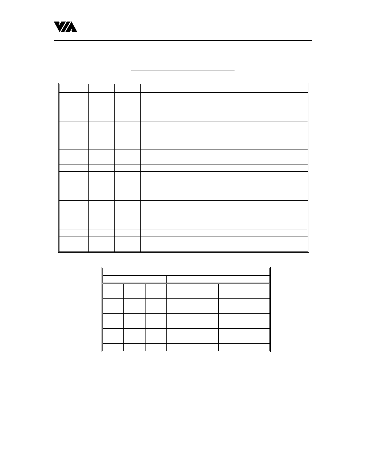
VT8225 Signal Descri ption
Symbol Pin No. Type Functions
X1
X2
S0
S1
S2
S3
MCLK 8 O Master clock output. Programmable output frequencies can
RESET# 11 O Chip reset, negative true.
TS 1 I
OSC 13 O 14.31818 Mhz output. Buffered output of on-chip reference
PD 6 O
VSS 7 Ground Digital Negative power supply.
AVSS 12 Ground Analog Negative power supply.
VDD 14 Power Positive power supply.
10
2
3
4
5
9
I
I/O
I
I
I
I
These pins form an on-chip reference oscillator when connected to
terminals of an external parallel resonant crystal (norminally
14.318Mhz). X1 may also serve as input for an externally
generated reference signal.
Frequency select inputs. These inputs control the MCLK frequency
selection. All these inputs have internal pull-ups. Table 1 below
shows the output frequency selection conditions.
be selected using So-S3.
Tri-state input pin. When high, all outputs are tri-stated. When low
outputs are enabled. This pin has an internal pull-down.
oscillaor or externally provided reference.
This is the phase detector output for the clock generator. It is
single-ended, tri-state output for use as loop error signal. A 0.1uF
capacitor to ground should be connected from this pin to form the
loop filter.
MCLK FREQUENCY SELECTION
INPUTS MCLK OUTPUT
S2 S1 S0 S3=1 (Bank 1) S3=0 (Bank 0)
0 0 0 8 Mhz 16 Mhz
0 0 1 20 Mhz 40 Mhz
0 1 0 25 Mhz 50 Mhz
0 1 1 40 Mhz 80 Mhz
1 0 0 33.3 Mhz 66.6 Mhz
1 0 1 50 Mhz 100 Mhz
1 1 0 4 Mhz 8 Mhz
1 1 1 2 Mhz 4 Mhz
Table 1 clock frequency selection
Note : The smooth transition of frequency change is only allowed within the same selection bank.
-2-
 Loading...