

VIA VT6508 Datasheet

VIA Technologies, Inc. Preliminary VT6508 Datasheet
VT6508
8 RMII PORTS OF 10/100BASE-T/TX
ETHERNET SWITCH CONTROLLER
REVISION ‘D’ DATASHEET
(Preliminary)
ISSUE 1: Nov 23, 1999
VIA Technologies, Inc.
1

VIA Technologies, Inc. Preliminary VT6508 Datasheet
PRELIMINARY RELEASE
Please contact VIA Technologies for the latest documentation.
Copyright Notice:
Copyright © 1995, VIA Technologies Incorporated. Printed in Taiwan. ALL RIGHTS
RESERVED.
No part of this document may be reproduced, transmitted, transcribed, stored in a retrieval
system, or translated into any language, in any form or by any means, electronic, mechanical,
magnetic, optical, chemical, manual or otherwise without the prior written permission of VIA
Technologies Incorporated.
The VT86C100P may only be used to identify products of VIA Technologies.
All trademarks are the properties of their respective owners.
Disclaimer Notice:
No license is granted, implied or otherwise, under any patent or patent rights of VIA
Technologies. VIA Technologies makes no warranties, implied or otherwise, in regard to this
document and to the products described in this document. The information provided by this
document is believed to be accurate and reliable to the publication date of this document.
However, VIA Technologies assumes no responsibility for any errors in this document.
Furthermore, VIA Technologies assumes no responsibility for the use or misuse of the
information in this document and for any patent infringements that may arise from the use of
this document. The information and product specifications within this document are subject to
change at any time, without notice and without obligation to notify any person of such change.
Offices:
1045 Mission Court 8th Floor, No. 533
Fremont, CA 94539 Chung-Cheng Rd., Hsin-Tien
USA Taipei, Taiwan ROC
Tel: (510) 683-3300 Tel: (886-2) 2218-5452
Fax: (510) 683-3301 Fax: (886-2) 2218-5453
Online Services:
BBS : 886-2-2186408
FTP : FTP.VIA.COM.TW
HTTP:WWW.VIA.COM.TW –or- WWW.VIATECH.COM
2

VIA Technologies, Inc. Preliminary VT6508 Datasheet
TABLE OF CONTENTS
TABLE OF CONTENTS................................................................................................................................3
FIGURES AND TABLES ...............................................................................................................................4
REVERSION HISTORY ................................................................................................................................5
FEATURES ................................................................................................................................................6
BLOCK DIAGRAM...................................................................................................................................... 9
FIGURE 1: FUNCTION BLOCK DIAGRAM OF VT6508. (NOTE THAT SOME INTERFACE
SIGNALS ARE ONLY AVAILABLE IN VT6509 OF 208-PIN PQFP PACKAGE.).............................. 9
PINOUT DIAGRAM................................................................................................................................... 10
FIGURE 2: PINOUT DIAGRAM OF VT6508. ...................................................................................... 10
PIN DESCRIPTIONS.................................................................................................................................. 11
DEFINITION OF VT6508B STRAPPING PINS .............................................................................................. 12
Pin.................................................................................................................................................... 12
SRAM TYPE: .................................................................................................................................... 12
SECTION I FUNCTIONAL DESCRIPTIONS...................................................................................... 15
1 GENERAL DESCRIPTION ...................................................................................................................... 15
2 THE VIA ETHER SWITCH ARCHITECTURE............................................................................................ 15
2.1 Switch initialization procedures .................................................................................................. 15
2.2 Packet Switching Flow ................................................................................................................ 16
2.3 PACKET BUFFERS AND FORWARDING TABLE ...................................................................................... 16
FIGURE 3. SRAM MEMORY LAYOUT............................................................................................... 17
FIGURE 4. DATA STRUCTURE OF FORWARDING TABLE SLOT................................................ 17
FIGURE 5. DATA STRUCTURE OF EMBEDDED LINK NODE. ...................................................... 17
2.3 RMII INTERFACE.............................................................................................................................. 19
2.3 MANAGEMENT INTERFACE AND AUTO NEGOTIATION ......................................................................... 19
2.4 FLOW CONTROL ............................................................................................................................... 21
FIGURE 6. XON/XOFF WINDOW CONCEPT..................................................................................... 23
2.5 BROADCAST STORM FILTERING......................................................................................................... 27
2.6 SERIAL EEPROM INTERFACE AND CONFIGURATION COMMANDS........................................................ 27
2.7 TRUNKING....................................................................................................................................... 28
3 THE VT6508 SRAM ADDRESS MAPPING TABLE............................................................... 30
SECTION II REGISTER MAP............................................................................................................... 31
1. REGISTERS TABLE ............................................................................................................................. 31
SECTION III ELECTRICAL SPECIFICATIONS................................................................................. 45
ABSOLUTE MAXIMUM RATINGS............................................................................................................... 45
DC CHARACTERISTICS............................................................................................................................ 45
AC CHARACTERISTICS............................................................................................................................ 46
PACKAGE MECHANICAL SPECIFICATIONS................................................................................................. 48
3

VIA Technologies, Inc. Preliminary VT6508 Datasheet
FIGURES AND TABLES
Figure 1: Function Block Diagram of VT6508. (Note that some interface signals are only
available in VT6509 of 208-pin PQFP package.)..................................................9
Figure 2: Pinout Diagram of VT6508. .......................................................................10
Figure 3. SRAM memory layout................................................................................17
Figure 4. Data structure of forwarding table slot........................................................17
Figure 5. Data structure of embedded link node.........................................................17
Figure 6. XON/XOFF Window Concept.................................................................... 23
4

VIA Technologies, Inc. Preliminary VT6508 Datasheet
REVERSION HISTORY
Reversion Date Reason for change By
V0.01 11/23/1999 First release version Murphy Chen
5

VIA Technologies, Inc. Preliminary VT6508 Datasheet
FEATURES
l Single chip 8 ports 10/100Mbps Ethernet switch controller
- Highly integrated single chip shared memory switch engine
- Supports 8 RMII (Reduced Media Independent Interface) ports
- Non-blocking layer 2 switch, 148,810 packets/sec on each 100Mbps Ethernet port
l Media Access Control (MAC)
- Dual 64-byte FIFO’s per port for receiving and transmitting
l Auto-sensing 10/100Mbps media speed, full/half -duplex mode, and flow-control
capability
l Two switching mechanisms
- Supports ‘store and forward’ switching with filtering CRC-bad packets
- Supports ‘cut through’ switching subject to long packets of length over 64 bytes
l Packet buffering
- Glueless 32-bit interface to SSRAM as a packet buffer pool
- 64 packet buffers for 32Kx32 SSRAM, 149 packet buffers for 64Kx32 SSRAM
- 1536 bytes for each packet buffer
l Storing control data (forwarding table and packet link entries) in external SSRAM
- Buffer status is stored in the internal free-buffer bit map registers
- Shared forwarding table of 2K entries (or 4K slots) to support multiple (up to 4K)
Mac addresses per port
l Efficient address recognition, self learning, and auto-aging mechanism
- Two-slot hashing algorithm to prevent hash collision
- Two optional hashing algorithms, CRC-map and direct-map
l Advanced congestion control mechanism
- IEEE 802.3X compliant flow control for full duplex ports
- Backpressure for half duplex ports
- Drop control for full duplex ports without flow control capability
- Incorporating with the output private buffering scheme to prevent HOL (head of line)
blocking
l Supports port mirroring (Sniffer feature)
l By-pass VLAN packets
l Support port-based trunking
- Support two individual trunk groups, each of 2 member ports
- Load balance according to DMAC address and source port number
l Support chip initialization through EEPROM or by strapping only
- Supports I2C EEPROM interface for customized configuration
- Supports LED serial-out in the strapping-only initialization mode
l 50MHz internal reference clock rate
l 83~100MHz SSRAM clock rate, typically 83MHz
l Single +3.3V supply, 0.3µm TSMC CMOS technology
l 128-pin PQFP package
6

VIA Technologies, Inc. Preliminary VT6508 Datasheet
7

VIA Technologies, Inc. Preliminary VT6508 Datasheet
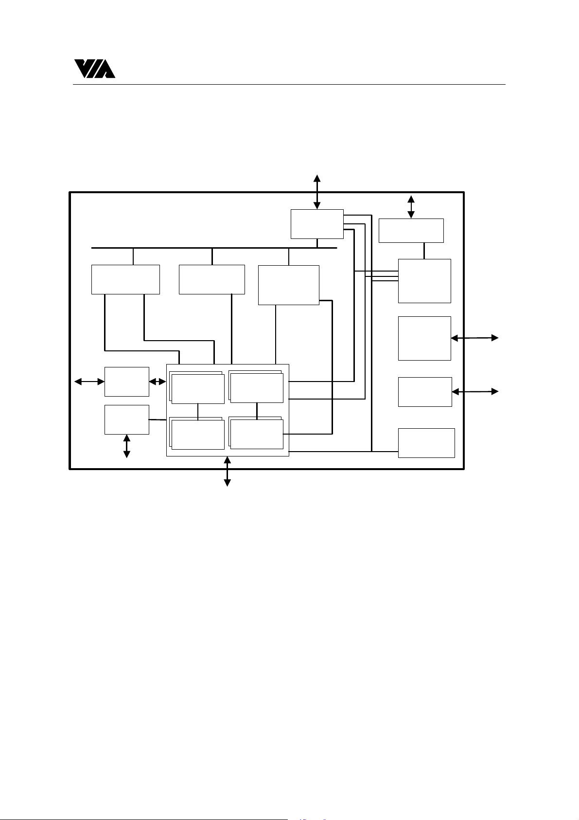
BLOCK DIAGRAM
VT6508
SRAM
Control
32-bit SRAM bus
8-bit
IDE bus
CPU Interface
Buffer Control
(fully bit-map
management)
Input
Input Control
Control
Ethernet
RMAC
RMAC
(flow control)
Output
Control
Ethernet
TMAC
RMII interface x 8
Queue
Control
CPU IO
Control
EEPROM
Control
(eeprom init)
PHY Control
(auto polling)
Scheduler
MII
interface
Forwarding
Table Control
(drop control)
RMII2MII
Translator
LED
Serial-Out
Control
LED
serial-out
bus
Figure 1: Function Block Diagram of VT6508. (Note that some interface signals are only
available in VT6509 of 208-pin PQFP package.)
Serial
EEPROM
interface
MII
management
interface
99/12/09 9
VIA Technologies, Inc. Preliminary VT6508 Datasheet
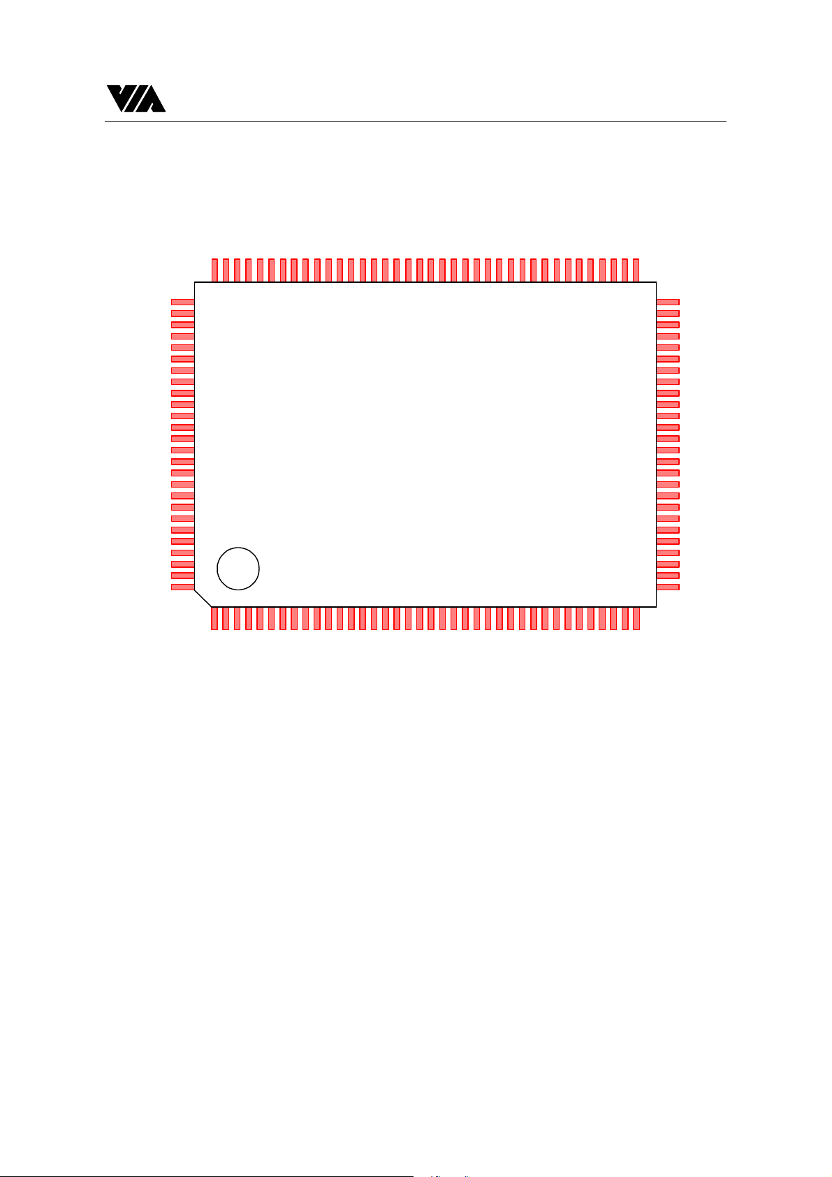
PINOUT DIAGRAM
SD11
SD10
SD9
100
101
102
SD8
VSS
SD7
SD6
SD5
SD4
SD3
VCC
SD2
SD1
SD0
EEIO/LEDIO
EEC/LEDC
SCLK
VCC
MDIO
MDC
TXD1_0
TXD0_0
TXEN_0
VSS
CSDV_0
RXD0_0
RXD1_0
TXD1_1
TXD0_1
103 SA13
104
105
106
107
108
109
110
111
112
113
114
115
116
117
118
119
120
121
122
123
124
125
126
127
128
1
VDD
99
GND
98
SD12
97
VCC
96
SD13
95
8765432
SD14
94
9
SD21
SD20
SD19
SD18
SD17
SD16
SD15
VSS
86
87
88
89
90
91
92
93
VT6508
17
16
15
14
13
12
11
10
SD22
85
18
VCC
84
19
SD23
83
20
SD24
82
21
SD25
81
22
SD26
80
23
VSS
79
24
SD27
78
25
SD28
77
26
SD29
76
27
SD30
75
28
SD31
74
29
VCC
73
30
SADS#
SWE#
71
72
32
31
SOE#
70
33
VDD
69
34
GND
68
35
VSS
67
36
SA15
66
37
SA14
65
64
63
62
61
60
59
58
57
56
55
54
53
52
51
50
49
48
47
46
45
44
43
42
41
40
39
38
SA12
SA11
VCC
SA10
SA9
SA8
SA7
SA6
VSS
SA5
SA4
SA3
SA2
SA1
VCC
RXD1_7
RXD0_7
CSDV_7
TXEN_7
TXD0_7
TXD1_7
RXD1_6
RXD0_6
CSDV_6
TXEN_6
TXEN_1
CSDV_1
GND
RXD0_1
VDD
RXD1_1
RESET#
TXD0_2
TXD1_2
TXEN_2
CSDV_2
RXD1_2
RXD0_2
RCLK50
TXD1_3
VCC
TXD0_3
TXEN_3
RXD0_3
CSDV_3
RXD1_3
TXD1_4
Figure 2: Pinout Diagram of VT6508.
TXD0_4
TXEN_4
RXD0_4
CSDV_4
RXD1_4
TXD1_5
TXD0_5
VSS
TXEN_5
CSDV_5
GND
RXD0_5
VDD
TXD1_6
RXD1_5
TXD0_6
99/12/09 10
VIA Technologies, Inc. Preliminary VT6508 Datasheet
SOE
SWE
SADS
RESET
PIN DESCRIPTIONS
No. Name Type Description
RMII interface
See Fig. 2
See Fig. 2
See Fig. 2
See Fig. 2
See Fig. 2
See Fig. 2
See Fig. 2
See Fig. 2
CSDV[7:0] I Carries sense and data valid from port 7 to port 0 :
RXD0[7:0] I Receive data zero from port 7 to port 0 :
RXD1[7:0] I Receive data one from port 7 to port 0 :
TXEN[7:0] O Transmit enable from port 7 to port 0 :
TXD0[7:0] O Transmit data zero from port 7 to port 0 :
TXD1[7:0] O Transmit data one from port 7 to port 0 :
SRAM Interface
SA[15:1] O
SRAM Address Bus:
15-bit SDRAM data bus. These signals connect directly to the address
input of the SDRAM devices.
O
Output Enable
See Fig. 2
See Fig. 2
See Fig. 2
See Fig. 2
See Fig. 2
See Fig. 2
See Fig. 2
See Fig. 2
See Fig. 2
See Fig. 2
O
O
SD[31:0] I/O
EEC/LEDC O
EEIO/LEDIO I/O
MDC O
MDIO I/O
RCLK50 I
SCLK I
I
SRAM Write Enable
Synchronous Processor Address Status
SRAM Data:
32-bit SRAM data bus. These signals connect directly to the data
input/output pins of the SRAM devices.
Miscellaneous Interface
Serial EEPROM Interface Clock (if strapping SD25 is default high)
The on-board EEPROM device address must be 1010 001 XXXXXXXX.
Serial LED Serial-Out Clock (if strapping SD25 is low)
The LEDC is 1MHz and has a burst per 50ms.
Serial EEPROM Interface Data (if strapping SD25 is default high)
Serial LED Serial-Out Data Output (if strapping SD25 is low)
Management Interface (MI) Clock Output
Management Interface (MI) Data I/O
50MHz Main Reference Clock
SRAM Reference Clock
The suggested clock rate is 83MHz or more high for non-blocking
requirement.
SYSTEM RESET
Power Supply & Ground
See Fig. 2
See Fig. 2
VDD P Positive 3.3V supply to the core digital logic.
VCC P Positive 3.3V supply to all I/O pads.
-11-

VIA Technologies, Inc. Preliminary VT6508 Datasheet
See Fig. 2
See Fig. 2
GND G Ground supply to the core digital logic.
VSS G Ground supply to all I/O pads.
DEFINITION OF VT6508B STRAPPING PINS
SD[31:0]: *Note that the default strapping bit value is “1”.
Pin Description
SD[0]
SD[1]
SD[2]
Broadcast or Drop BPDU Packets:
BCAST_BPDU == 1’ b1 => broadcast BPDU packet if CPU_FWD_CFG[1] == 0
(default)
BCAST_BPDU == 1’ b0 => drop BPDU packet if CPU_FWD_CFG[1] == 0
Note that BPDU packets will be forwarded to CPU port if CPU_FWD_CFG[1] == 1
without regard to the value of BCAST_BPDU.
LED Display Combination of Link Activity Status with RX/TX Event:
LED_COMB [0] == 1’ b1 => combined (default)
LED_COMB [0] == 1’ b0 => not combined
Note that the LED bit sequence [10:1] is used originally to display link activity status. By
setting combination with RX/TX event, it will indicate both the link activity status and
RX/TX events so that required LED number can be reduced.
Enable Drop Control for Private Buffer Reservation:
DROP_CONTROL_EN [0] == 1’ b1 => enabled (default)
DROP_CONTROL_EN [1] == 1’ b0 => disabled
SD[3]
SD[5:4]
Note that drop control has a lower priority than flow control and backpressure.
If it is disabled, all TMACs will not make the drop window signals to Forwarding Control.
If it is enabled and the flow control/backpressure mechanism is not enabled, all TMACs
will make the drop window signals to Forwarding Control.
If it is enabled and the flow control mechanism is also enabled, but the full-duplex party
has no flow control capability, TMAC will make the drop window signal to Forwarding
Control.
SRAM TYPE:
SRAM_TYPE == 1’ b1 => 64Kx32 (default)
SRAM_TYPE == 1’ b0 => 32Kx32
size=128KB: FREEMCNT=64, XON_THRED=43, PRIVATE_BUF_SIZE=1
V_FREE=10, MIN_XOFF_CONST_THRED=15
size=256KB: FREEMCNT=149, XON_THRED=98, PRIVATE_BUF_SIZE=4
V_FREE=10, MIN_XOFF_CONST_THRED=28
CHIP INIT MODE [1:0]:
CHIP_INIT[1:0] == 2’ b11 => Chip Initialization via strapping only (default)
CHIP_INIT[1:0] == 2’ b10 => Chip Initialization via EEPROM
CHIP_INIT[1:0] == 2’ b01 => Chip Initialization via CPU
CHIP_INIT[1:0] == 2’ b00 => Chip Initialization via EEPROM in speedup mode
In none speedup mode, EEC = 78.125K Hz, LED period = 50ms.
In speedup mode for testing, EEC = 2.778MHz, LED period = 1ms without one-second
flash.
-12-

VIA Technologies, Inc. Preliminary VT6508 Datasheet
SD[7:6]
SD[15:8]
SD[17,16]
SD[18]
SD[20:19]
SD[23:21]
Number of Tries of Excessive Collisions Before Dropping:
RETRY_EXCE_COLL [1:0] == 2’ b11 => 3 tries (default)
RETRY_EXCE_COLL [1:0] == 2’ b10 => 2 tries
RETRY_EXCE_COLL [1:0] == 2’ b01 => retry forever
RETRY_EXCE_COLL [1:0] == 2’ b00 => 1 try
Internally, retry_no = RETRY_EXCE_COLL, or infinite if it is zero.
By default, after 3 tries (i.e. 3 turns of (excessive) 16 collisions), the outgoing packet will
be dropped.
(reserved with default value “pull-high”)
Trunking Mode:
SD16 == 1, port (0,1) no trunking (default)
0, port (0,1) in trunking mode,
SD17 == 1, port (6,7) no trunking (default)
0, port (6,7) in trunking mode.
To simplify layout, trunk group (6,7) can connect with neighboring (right-side)
VT6508’ s trunk group (0,1) in on-board manner.
Note that on-board trunk ports do not need auto-polling and they must be full-duplex &
100Mbps ports & forced flow control enable mode.
Enable Backpressure:
BACKPRESSURE_EN [0] == 1’ b1 => enabled (default)
BACKPRESSURE_EN [1] == 1’ b0 => disabled
Note that if it is disabled, all TMAC of half-duplex ports will ignore the flow control
XON/XOFF signals from Queue Control.
Enable RMII Port Flow Control:
RMII_PORT_FC_EN[1:0] == 2’ b11 => for RMII ports, set self flow control ability
register bit and detect party’ s flow control ability (default)
RMII_PORT_FC_EN[1:0] == 2’ b10 => for RMII ports, disable self flow control ability
register bit and assume (ignore auto-polling) party has no flow control capability
RMII_PORT_FC_EN[1:0] == 2’ b01 => for RMII ports, enable self flow control ability
register bit and assume (ignore auto-polling) party has flow control capability
RMII_PORT_FC_EN[1:0] == 2’ b00 => same as 2’ b11.
While enabled (RMII_PORT_FC_EN[1:0] == 2’ b11 or 2’ b00), set self each PHY
device’ s flow control ability register bit PHY_ANAR_4.10 as 1, and auto polling
PHY_ANLPAR_5.10 to check whether the party has the flow control capability.
While forced disabling (RMII_PORT_FC_EN[1:0] == 2’ b10), set self PHY devices’
flow control ability register bit PHY_ANAR_4.10 as 0 (no such capability), and does not
need auto polling PHY_ANLPAR_5.10.
While forced disabling (RMII_PORT_FC_EN[1:0] == 2’ b01), set self PHY devices’
flow control ability register bit PHY_ANAR_4.10 as 1 (with flow control capability), and
does not need auto polling PHY_ANLPAR_5.10.
For forced disabling, turn off flow control enable bits of all RMII ports.
For (forced) enabling, turn on flow control enable bits of all RMII ports.
LED Serial-Out Mask for Groups 0,1,2,3 [3:0]:
LED_MASK[0] == 1’ b1 => enable group 0 data out (default)
LED_MASK[1] == 1’ b1 => enable group 1 data out (default)
LED_MASK[2] == 1’ b1 => enable group 2 data out (default)
LED Groups 3,4,5 serial out is always enabled. The time period of LED sequence is
50ms.
-13-

VIA Technologies, Inc. Preliminary VT6508 Datasheet
SD[24]
SD[25]
SD[26]
SD[27]
SD[28]
Hash Algorithm Selection:
HASH_ALG_SEL == 1 => CRC-map with scramble (default)
HASH_ALG_SEL == 0 => Direct-map without scramble
HASH_ALG_SEL == 1 will make the register HASH_ALG[1:0]=0 that is helpful to the
X-Stream test.
HASH_ALG_SEL == 0 will make the register HASH_ALG[1:0]=3 that can get a good
result of 4094 MAC addresses in Address Handling test.
No Swap EEPROM and LED output pins:
NO_SWAP_EEPROM_LED == 1 => The pins 192/193 are used as
EEIO/EEC. (default)
NO_SWAP_EEPROM_LED == 0 => The pins 192/193 are used as
LEDIO/LEDC.
In 128-pin package, we can bond this pin to VSS to select LED output from the original
EEPROM output pins.
Enable Aging:
EN_AGING == 1 => enable aging function (default)
EN_AGING == 0 => disable aging function
Disable Cut Through Enable:
DIS_CUT_THRU == 1 => disable cut-through feature
(default, i.e. store & forward)
DIS_CUT_THRU == 0 => enable cut-through feature
Disable Aggressive Backoff Algorithm:
DIS_AGGRES_BACKOFF == 1’ b1 => disabled (default)
DIS_AGGRES_BACKOFF == 1’ b0 => enabled
SD[29]
SD[30]
SD[31]
Note that if this feature is enabled, the backoff algorithm for all Ethernet ports is in MBA
mode. By default, the backoff algorithm bits MBA=0 and OFSET=1.
Backpreasure Collision Point Configuration:
COLL_POINT_CFG == 1 => 32th byte (default)
COLL_POINT_CFG == 0 => 2nd byte
Disable TEST mode:
DIS_TEST_MODE == 1 => disabled (default)
DIS_TEST_MODE == 1 => enabled
Disable Latchup Mode:
DIS_LATCH_UP_MODE == 1’ b1 => disable Latchup mode (default)
DIS_LATCH_UP_MODE == 1’ b0 => enable Latchup mode, all output only IO PADs
are in tri-state after reset.
-14-

VIA Technologies, Inc. Preliminary VT6508 Datasheet
SECTION I FUNCTIONAL DESCRIPTIONS
1 GENERAL DESCRIPTION
The VT6508 is a low-cost switch engine chip implementation of an 8 ports 10/100Mbps
Ethernet switch system for IEEE 802.3 and IEEE 802.3u networks. Each port can be either
auto-sensing or manually selected via EEPROM configuration to run at 10Mbps or 100Mbps
speed rate, full or half duplex mode.
The VT6508 supports RMII (reduce MII) port interface. There are eight independent MACs
within the VT6508 chip. The MAC controller controls the receiving, transmitting, and
deferring of each individual port, and the MAC controller also provides framing, FCS
checking, error handling, status indication and flow control function. It has wire-speed
performance with forwarding rate of 148,810 packets/sec on each 100Mbps Ethernet port.
The VT6508 can be configured via EEPROM or strapping only.
2 THE VIA ETHER SWITCH ARCHITECTURE
The VT6508 switch engine uses the shared memory architecture. In order to improve the
packet latency, VT6508 provides two methods for packet switching, cut-through and storeand-forwarding.
2.1 Switch initialization procedures
Step_1. Read strapping signal.
Step_2 Write Reg 0619H with WR_DATA = 8’h01 to trigger SRAM_Ctrl module auto-
test.
Step_3. If initialization by Strapping, then go to Step_4.
If initialization by EEPROM, eeprom_ctrl module will download register data
from EEPROM (by internal register bus IOW, CS_*, IO_ADDR, and
IO_WR_DATA).
If EEPROM data download error, then go to step6.
Step_4 After SRAM auto-test completed, write Reg 0304H with WR_DATA = 8’h01 to
trigger Forward_Ctrl module auto aging.
Step_5 Write Reg 0404H with WR_DATA = 8’h08 to trigger PHY_Ctrl module
phy_auto-polling.
Step_6 Write Reg 000aH with WR_DATA = 8’h01 to trigger LED_Ctrl module to
display LED.
Step_7 Chip initialization done.
-15-
 Loading...