

Via CN400 User Manual

Data Sheet
CN400
North Bridge
with Integrated UniChrome
Pro 3D / 2D Graphics
Controller
Revision 1.18
January 26, 2005
VIA TECHNOLOGIES, INC.

Copyright Notice:
Copyright © 2003-2005 VIA Technologies Incorporated. All Rights Reserved. No part of this document may be reproduced, transmitted,
transcribed, stored in a retrieval system, or translated into any language, in any form or by any means, electronic, mechanical, magnetic, optical,
chemical, manual or otherwise without the prior written permission of VIA Technologies Incorporated. The material in this document is for
information only and is subject to change without notice. VIA Technologies Incorporated reserves the right to make changes in the product design
without reservation and without notice to its users.
Copyright © 2003-2005 S3 Graphics Incorporated. All rights reserved. If you have received this document from S3 Graphics Incorporated in
electronic form, you are permitted to make the following copies for business use related to products of S3 Graphics Incorporated: one copy onto
your computer for the purpose of on-line viewing, and one printed copy. With respect to all documents, whether received in hard copy or electronic
form, other use, copying or storage, in whole or in part, by any means electronic, mechanical, photocopying or otherwise, is not permitted without the
prior written consent of S3 Graphics Incorporated. The material in this document is for information only and is subject to change without notice. S3
Graphics Incorporated reserves the right to make changes in the product design without reservation and without notice to its users.
Trademark Notices:
VT8237R and CN400 may only be used to identify products of VIA Technologies.
C3™ and PowerSaver™ are registered trademarks of VIA Technologies.
Windows XP™, Windows 2000™, Windows ME™, Windows 98™ and Plug and Play™ are registered trademarks of Microsoft Corporation.
AGP™ is a trademark of the AGP Implementors Forum.
PCI™ is a registered trademark of the PCI Special Interest Group.
All trademarks are the properties of their respective owners.
Disclaimer Notice:
No license is granted, implied or otherwise, under any patent or patent rights of VIA Technologies or S3 Graphics. VIA Technologies and S3
Graphics make no warranties, implied or otherwise, in regard to this document and to the products described in this document. The information
provided by this document is believed to be accurate and reliable as of the publication date of this document. However, VIA Technologies and S3
Graphics assume no responsibility for any errors in this document. Furthermore, VIA Technologies and S3 Graphics assume no responsibility for
the use or misuse of the information in this document and for any patent infringements that may arise from the use of this document. The
information and product specifications within this document are subject to change at any time, without notice and without obligation to notify any
person of such change.
Offices:
VIA Technologies Incorporated
Taiwan Office:
st
Floor, No. 531
1
Chung-Cheng Road, Hsin-Tien
Taipei, Taiwan ROC
Tel : (886-2) 2218-5452
Fax : (886-2) 2218-5453
Home page :
http://www.via.com.tw
VIA Technologies Incorporated
USA Office:
940 Mission Court
Fremont, CA 94539
USA
Tel : (510) 683-3300
Fax : (510) 683-3301 or (510) 687-4654
Home Page:
http://www.viatech.com
S3 Graphics Incorporated
USA Office:
1045 Mission Court
Fremont, CA 94539
USA
Tel : (510) 687-4900
Fax : (510) 687-4901
Home Page:
http://www.s3graphics.com
CN400 Data Sheet
REVISION HISTORY
Document Release Date Revision Initials
1.0 3/25/04 Initial external release – same as internal release 0.91 published 2/19/04 DH
1.1 4/29/04 Fixed GTVCLKIN pin descriptions; Changed GDVP0xxx to GTV0xxx in pin lists
Updated DVP0D[6:4] strap definitions; Added F3Rx52-53; Changed F7Rx57 to RO
1.11 5/18/04 Republished to fix PDF file color problems; Fixed GTVCLKIN pin name in table 3
Removed “Mobile” (chipset is used for both mobile and desktop systems)
Fixed DVP0D8,6-4 strap definitions (replaced 6-4 strap definitions from revision 1.0)
Fixed VIA logo shape in marking specs
1.12 6/8/04 Added NMI function to AGPBUSY pin DH
1.13 6/10/04 Fixed spelling error typo in GADSTB1F pin name DH
1.14 6/21/04 Removed D0F2 Rx55[5], 57, 74[7-6,3-0], 78 (changed to reserved, always reads 0)
Changed 4x to 1x in D0F2Rx72-73 register names and Rx75[7], 77[3-0] bit names
1.15 8/11/04 Changed feature bullets & marking specs to show “lead-free” package DH
1.16 8/30/04 Removed registered DIMM support DH
1.17 9/29/04 Renamed TMDS to DVI
Updated south bridge to VT8237
Updated system block diagram and table 1
Added HDTV feature in overview section
Removed Pentium 3 in the figure on page 18
Modified overview heading and table caption of pin lists table
Added lead free mechanical package diagram
1.18 1/26/05 Updated copyright year in legal page
Changed south bridge marketing name from VT8235 and VT8237 to VT8235M and VT8237R
Added CN400 AC – Timing Relationship Table and Diagram
DH
DH
DH
SV
SV
Revision 1.18, January 26, 2005 -i- Revision History

CN400 Data Sheet
TABLE OF CONTENTS
REVISION HISTORY .......................................................................................................................................................................I
TABLE OF CONTENTS.................................................................................................................................................................. II
LIST OF FIGURES .........................................................................................................................................................................IV
LIST OF TABLES ...........................................................................................................................................................................IV
PRODUCT FEATURES.................................................................................................................................................................... 1
CN400 SYSTEM OVERVIEW......................................................................................................................................................... 6
VIA C3 PROCESSOR INTERFACE.................................................................................................................................................. 6
MEMORY CONTROLLER................................................................................................................................................................ 6
ULTRA V-LINK .............................................................................................................................................................................. 7
SYSTEM POWER MANAGEMENT ................................................................................................................................................... 7
3D GRAPHICS ENGINE................................................................................................................................................................... 7
128-BIT 2D GRAPHICS ENGINE ..................................................................................................................................................... 7
MPEG VIDEO PLAYBACK............................................................................................................................................................. 7
VIDEO CAPTURE ............................................................................................................................................................................ 7
LCD, DVI MONITOR AND TV OUTPUT DISPLAY SUPPORT ........................................................................................................ 8
DESKTOP MODES FOR SINGLE DISPLAY....................................................................................................................................... 9
PINOUTS.......................................................................................................................................................................................... 10
PIN DIAGRAMS............................................................................................................................................................................. 10
PIN LISTS ..................................................................................................................................................................................... 12
PIN DESCRIPTIONS....................................................................................................................................................................... 17
CPU Interface Pin Descriptions .......................................................................................................................................... 17
DDR SDRAM Memory Controller Pin Descriptions......................................................................................................... 18
Accelerated Graphics Port Pin Descriptions...................................................................................................................... 19
Ultra V-Link Pin Descriptions............................................................................................................................................. 21
CRT and Serial Bus Pin Descriptions................................................................................................................................. 22
Dedicated Digital Video Port 0 (DVP0) Pin Descriptions ................................................................................................. 23
AGP-Multiplexed Flat Panel Display Port (FPDP) Pin Descriptions............................................................................... 25
AGP-Multiplexed Digital Video Port 1 (GDVP1) Pin Descriptions ................................................................................. 27
Clock, Reset, Power Control, GPIO, Interrupt and Test Pin Descriptions..................................................................... 28
Compensation and Reference Voltage Pin Descriptions ................................................................................................... 29
Power Pin Descriptions ........................................................................................................................................................ 30
Strap Pin Descriptions.......................................................................................................................................................... 31
REGISTERS..................................................................................................................................................................................... 32
REGISTER OVERVIEW ................................................................................................................................................................. 32
MISCELLANEOUS I/O................................................................................................................................................................... 40
CONFIGURATION SPACE I/O ....................................................................................................................................................... 40
DEVICE 0 FUNCTION 0 REGISTERS - AGP.................................................................................................................................. 41
Device 0 Function 0 Header Registers ................................................................................................................................ 41
Device 0 Function 0 Device-Specific Registers ................................................................................................................... 43
AGP Drive Control................................................................................................................................................................................ 43
AGP Miscellaneous Control.................................................................................................................................................................. 43
AGP Power Management Control......................................................................................................................................................... 44
AGP GART / Graphics Aperture...........................................................................................................................................................45
Revision 1.18, January 26, 2005 -ii- Table of Contents

CN400 Data Sheet
AGP 3.0 Registers ................................................................................................................................................................................. 46
AGP Enhanced Control ......................................................................................................................................................................... 47
DEVICE 0 FUNCTION 1 REGISTERS – ERROR REPORTING......................................................................................................... 50
Device 0 Function 1 Header Registers ................................................................................................................................ 50
Device 0 Function 1 Device-Specific Registers ................................................................................................................... 51
V-Link Error Reporting......................................................................................................................................................................... 51
AGP Error Reporting............................................................................................................................................................................. 51
DEVICE 0 FUNCTION 2 REGISTERS – HOST CPU....................................................................................................................... 52
Device 0 Function 2 Header Registers ................................................................................................................................ 52
Device 0 Function 2 Device-Specific Registers ................................................................................................................... 53
Host CPU Control .................................................................................................................................................................................53
Host CPU AGTL+ I/O Control .............................................................................................................................................................57
DEVICE 0 FUNCTION 3 REGISTERS – DRAM............................................................................................................................. 58
Device 0 Function 3 Header Registers ................................................................................................................................ 58
Device 0 Function 3 Device-Specific Registers ................................................................................................................... 59
DRAM Control...................................................................................................................................................................................... 59
ROM Shadow Control........................................................................................................................................................................... 67
DRAM Above 4G Control ....................................................................................................................................................................68
UMA Control ........................................................................................................................................................................................69
Graphics Control ................................................................................................................................................................................... 70
AGP Controller Interface Control .........................................................................................................................................................70
DRAM Drive Control............................................................................................................................................................................ 71
DEVICE 0 FUNCTION 4 REGISTERS – POWER MANAGEMENT ................................................................................................... 72
Device 0 Function 4 Header Registers ................................................................................................................................ 72
Device 0 Function 4 Device-Specific Registers ................................................................................................................... 73
Power Management Control.................................................................................................................................................................. 73
BIOS Scratch......................................................................................................................................................................................... 73
DEVICE 0 FUNCTION 7 REGISTERS – V-LINK ............................................................................................................................ 74
Device 0 Function 7 Header Registers ................................................................................................................................ 74
Device 0 Function 7 Device-Specific Registers ................................................................................................................... 75
V-Link Control...................................................................................................................................................................................... 75
PCI Bus Control ....................................................................................................................................................................................78
Graphics Aperture Control ....................................................................................................................................................................80
V-Link CKG Control............................................................................................................................................................................. 80
V-Link Compensation / Drive Control.................................................................................................................................................. 81
DRAM Above 4G Support.................................................................................................................................................................... 81
DEVICE 1 REGISTERS – PCI-TO-PCI BRIDGE............................................................................................................................ 82
Device 1 Header Registers.................................................................................................................................................... 82
Device 1 Device-Specific Registers ...................................................................................................................................... 84
AGP Bus Control................................................................................................................................................................................... 84
ELECTRICAL SPECIFICATIONS .............................................................................................................................................. 87
ABSOLUTE MAXIMUM RATINGS ................................................................................................................................................. 87
DC CHARACTERISTICS ............................................................................................................................................................... 87
AC CHARACTERISTICS ............................................................................................................................................................... 87
MECHANICAL SPECIFICATIONS............................................................................................................................................. 89
Revision 1.18, January 26, 2005 -iii- Table of Contents

CN400 Data Sheet
LIST OF FIGURES
FIGURE 1. SYSTEM BLOCK DIAGRAM.................................................................................................................................... 6
FIGURE 2. INTEGRATED UNICHROME PRO GRAPHICS CONTROLLER INTERNAL BLOCK DIAGRAM ............ 8
FIGURE 3. BALL DIAGRAM (TOP VIEW) – FLAT PANEL / DIGITAL VIDEO OUTPUT ENABLED (NO
EXTERNAL AGP INTERFACE)............................................................................................................................. 10
FIGURE 4. BALL DIAGRAM (TOP VIEW) - EXTERNAL AGP INTERFACE ENABLED ON DISPLAY PINS............ 11
FIGURE 5. GRAPHICS APERTURE ADDRESS TRANSLATION......................................................................................... 45
FIGURE 6. CN400 AC-TIMING RELATIONSHIP DIAGRAM............................................................................................... 88
FIGURE 7. MECHANICAL SPECIFICATIONS - 681-PIN HSBGA BALL GRID ARRAY PACKAGE WITH HEAT
SPREADER................................................................................................................................................................. 89
FIGURE 8. LEAD-FREE MECHANICAL SPECIFICATIONS - 681-PIN HSBGA BALL GRID ARRAY PACKAGE
WITH HEAT SPREADER........................................................................................................................................ 90
LIST OF TABLES
TABLE 1. SUPPORTED CRT AND PANEL SCREEN RESOLUTIONS.................................................................................. 9
TABLE 2. PIN LIST (LISTED BY PIN NUMBER) – DISPLAY INTERFACE ENABLED (NO EXTERNAL AGP) ........ 12
TABLE 3. PIN LIST (LISTED BY PIN NAME) - DISPLAY INTERFACE ENABLED (NO EXTERNAL AGP) .............. 13
TABLE 4. PIN LIST (LISTED BY PIN NUMBER) - EXTERNAL AGP INTERFACE ENABLED (NO PANEL
INTERFACE) ............................................................................................................................................................... 14
TABLE 5. PIN LIST (LISTED BY PIN NAME) - EXTERNAL AGP INTERFACE ENABLED (NO PANEL
INTERFACE) ............................................................................................................................................................... 15
TABLE 6. POWER, GROUND AND VOLTAGE REFERENCE PIN LIST............................................................................ 16
TABLE 7. REGISTERS ................................................................................................................................................................. 32
TABLE 8. SYSTEM MEMORY MAP.......................................................................................................................................... 59
TABLE 9. DIMM MA SETTING.................................................................................................................................................. 59
TABLE 10. MA MAP TYPE ENCODING ................................................................................................................................... 60
TABLE 11. 1X BANDWIDTH (64-BIT DDR) MEMORY ADDRESS MAPPING TABLE.................................................... 66
TABLE 12. VGA/MDA MEMORY/IO REDIRECTION ........................................................................................................... 84
TABLE 13. ABSOLUTE MAXIMUM RATINGS....................................................................................................................... 87
TABLE 14. DC CHARACTERISTICS......................................................................................................................................... 87
TABLE 15. CN400 AC – TIMING RELATIONSHIP TABLE .................................................................................................. 87
Revision 1.18, January 26, 2005 -iv- Lists of Figures and Tables

CN400 Data Sheet
CN400 NORTH BRIDGE
200 / 133 / 100 MHz VIA C3 Front Side Bus
Integrated UniChrome Pro 3D / 2D Graphics & Video Controllers
Advanced DDR400 SDRAM Controller
1 GB / Sec Ultra V-Link Interface
External 8x / 4x AGP Bus
PRODUCT FEATURES
• Defines Highly Integrated Solutions for Full Featured, Power Efficient PC Designs
– High Performance UMA North Bridge: Integrated VIA C3 North Bridge with 200 MHz FSB support and
UniChrome Pro 3D / 2D Graphics & Video Controllers in a single chip
– Advanced memory controller supporting DDR400 / 333 / 266 / 200 SDRAM
– Combines with VIA VT8235M-CE / VT8237R South Bridge for integrated 10/100 LAN, Audio, ATA133 IDE, LPC,
USB 2.0 and Serial ATA (VT8237R)
– “Lead-free” 31 x 31mm HSBGA (Ball Grid Array with Heat Spreader) package with 681 balls and 1mm ball pitch
• High Performance CPU Interface
– Supports 200 / 133 / 100 MHz FSB VIA C3 processors
– Eight outstanding transactions (eight-level In-Order Queue (IOQ))
– Built-in Phase Lock Loop circuitry for optimal skew control within and between clocking regions
• Full Featured Accelerated Graphics Port (AGP) Controller
– AGP v3.0 compliant 8x / 4x transfer mode with Fast Write support
– 1.5V AGP I/O interface
– Pipelined split-transaction long-burst transfers up to 2.1 GB / Sec
– Supports Side Band Addressing (SBA) mode
– Supports Flush / Fence commands
– Supports DBI (Dynamic Bus Inversion)
– Asynchronous AGP and CPU interface
– Thirty-two level request queue for read and write
– Sixty-four level (quadwords) of read data FIFO
– Sixty-four level (quadwords) of write data FIFO
– Graphics Address Relocation Table (GART)
– One level TLB structure
– Sixteen entry fully associative page table
– LRU replacement scheme
Revision 1.18, January 26, 2005 -1- Product Features

CN400 Data Sheet
• Advanced High-Performance 64-Bit DDR SDRAM Controller
– Supports DDR400 / 333 / 266 memory types with 2.5V SSTL-2 DRAM interface
– Supports mixed 64 / 128 / 256 / 512 / 1024Mb DDR SDRAMs in x8 and x16 configurations
– Supports CL 2 / 2.5 for DDR266 / 333 and CL 2.5 / 3 for DDR400
– Supports 2 unbuffered double-sided DIMMs and up to 4 GBytes of physical memory
– Programmable timing / drive for memory address, data and control signals
– DRAM interface pseudo-synchronous with host CPU for optimal memory performance
– Concurrent CPU, internal graphics controller and V-Link access for minimum memory access latency
– Rank interleave and up to 16-bank page interleave (i.e., 16 pages open simultaneously) based on LRU to effectively
reduce memory access latency
– Seamless DRAM command scheduling for maximum DRAM bus utilization
– (e.g., precharge other banks while accessing the current bank)
– CPU Read-Around-Write capability for non-stalled operation
– Speculative DRAM read before snoop result to reduce PCI master memory read latency
– Supports Burst Read and Write operations with burst length of 4 or 8
– Eight cache lines (64 quadwords) of integrated CPU-to-DRAM write buffers and eight separate cache lines of CPU-
to-DRAM read prefetch buffers
– Optional dynamic Clock Enable (CKE) control for DRAM power reduction during normal system state (S0)
– Supports self-refresh and CAS-before-RAS DRAM refresh with staggered RAS timing
• High Bandwidth 1 GB / Sec 16-Bit “Ultra V-Link” Host Controller
– Supports 66 MHz, 4x and 8x transfer modes, Ultra V-Link Host interface with 1 GB / Sec total bandwidth
– Full duplex transfers with separate command / strobe for 4x and 8x modes
– Request / Data split transaction
– Transaction assurance for V-Link Host-to-Client access eliminates V-Link Host-Client Retry cycles
– Intelligent V-Link transaction protocol to eliminate data wait-state / throttle transfer latency and avoid data overflow
– Highly efficient V-Link arbitration with minimum overhead
• Advanced System Power Management Support
– ACPI 2.0 and PCI Bus Power Management 1.1 compliant
– Supports Suspend-to-DRAM (STR) and DRAM self-refresh
– Supports dynamic Clock Enable (CKE) control for DRAM power reduction during normal system state (S0)
– Supports SMI, SMM and STPCLK mechanisms
– Supports VIA PowerSaver™ Technology
– Low-leakage I/O pads
Revision 1.18, January 26, 2005 -2- Product Features
CN400 Data Sheet
• Integrated Graphics with 2D / 3D / Video Controllers
– Optimized Unified Memory Architecture (UMA)
– Supports 16 / 32 / 64 MB Frame Buffer sizes
– 200 MHz Graphics Engine Clock
– Two independent 128-bit data paths between North Bridge and graphics core to improve video performance, one for
frame buffer access and one for texture / command access
– PCI v2.2 Host Bus compliant
– AGP v3.0 compliant
2D Acceleration
– 128-bit 2D graphics engine
– Hardware 2D rotation
– Supports ROP3, 256 operations
– Supports 8bpp, 15/16bpp and 32bpp color depth modes
– BitBLT (Bit BLock Transfer) functions including alpha BLTs
– True-color hardware cursor (64x64x32bpp) with 256-level blending effect
– Color expansion, source Color Key and destination Color Key
– Bresenham line drawing / style line function
– Transparency mode
– Window clipping
– Text function
3D Acceleration
3D Graphics Processor
– 128-bit 3D graphics engine
– Dual pixel rendering pipes and dual texture units
– Floating-point setup engine
– Internal full 32-bit ARGB format for high rendering quality
– 8K Texture Cache
Capability
– Supports ROP2
– Supports various texture formats including 16/32bpp ARGB, 8bpp Palletized (ARGB), YUV 422/420 and
– Texture sizes up to 2048x2048 with Microsoft DirectX texture compression
– High quality texture filter for Nearest, Linear, Bi-linear, Tri-linear and Anisotropic modes
– Flat and Gouraud shading
– Vertex Fog and Fog Table
– Z-Bias, LOD-Bias, Polygon offset, Edge Anti-aliasing and Alpha Blending
– Bump mapping and cubic mapping
– Hardware back-face culling
– Specular lighting
Performance
– Two textures per pass
– Triangle rate up to 4.5 million triangles per second
– Pixel rate up to 200 million pixels per second for 2 textures each
– Texel bilinear fill rate up to 400 million texels per second
– High quality dithering
compressed texture (DXTC)
Revision 1.18, January 26, 2005 -3- Product Features

CN400 Data Sheet
Video Acceleration
High Quality Video Processor
– RGB555, RGB565, RGB8888 and YUV422 video playback formats
– High quality 5-tap horizontal and 5-tap vertical scaler (up or down) for both horizontal and vertical scaling
(linear interpolation for horizontal and vertical p-scaling and filtering for horizontal and vertical down-scaling)
– Independent graphics and video gamma tables
– 2 sets of Color and Chroma Key support
– Color enhancement for contrast, hue, saturation and brightness
– YUV-to-RGB color space conversion
– Display rotation in clockwise and counter-clockwise directions
– Bob, Weave, Median-filter and Adaptive de-interlacing modes
– 3:2 / 2:2 pull-down detection
– De-blocking mode support
– Combining of many special effects such as filter, scaling up or down, sub-picture blending, de-interlacing and
deblocking to one pass process
– Tear-free double / triple buffer flipping
– Input video vertical blanking or line interrupt
– Video gamma correction
Video Overlay Engine
– Simultaneous graphics and TV video playback overlay
– Supports video window overlays
– Supports both YUV and RGB format Chroma Key
– Supports 16 operations for Color and Chroma Key
– Hardware sub-picture blending
MPEG Video Playback
– MPEG-2 hardware VLD (Various Length Decode), iDCT, and motion compensation for full speed DVD and
MPEG-2 playback at full D1 resolution
– MPEG-4 ASP (Advanced Simple Profile) Level 5 with GMC (Global Motion Compensation) L0/L1 and ¼-pixel
MC support for high video quality and performance
– High quality DVD and streaming video playback
– Video auto-flipping
– Hardware DVD sub-picture blending
Video Capture Capability
– Dual-8-bit or single-16-bit capture port following ITU-R BT656, VIP 1.1 and VIP 2.0 standards supporting 16 / 32-
bit RGB and YUV422 video capture formats
– Video capture and playback tear free auto flipping
– Multiplexed on Digital Video Port 0 (DVP0 selectable as Capture-In or TV-Out)
– External Hsync / Vsync support (on the 16-bit port or on the first of the two 8-bit ports)
DuoView+™ Dual Image Capability
– WinXP, WinME and Win98 multi-monitor, extended desktop support
– Two independent display engines, each of which can display completely different information at different
resolutions, pixel depths and refresh rates (supports different images on different displays simultaneously)
– CRT, FPD, DVI monitor and TV refresh rates are independently programmable for optimum image quality
– Improved display flexibility with simultaneous FPD / CRT, FPD / TV, FPD / DVI and other combined operations
Full Software Support
– Microsoft DirectX 7.0, 8.0 and 9.0 compatible
– Microsoft DirectX Texture Compression (DXTC / S3TC)
– Supports OpenGL
– Drivers for major operating systems and APIs: Windows
DirectDraw, DirectShow and OpenGL ICD for Windows 9x/ME and XP
– Windows NT 4.0 Standard VGA driver
Revision 1.18, January 26, 2005 -4- Product Features
9x/ME, Windows 2000, Windows XP, Direct3D,
CN400 Data Sheet
• Extensive Display Support for External Video Output
– CRT display interface
– 12-bit Digital Video Port with support for TV Out or Video Capture In
– 12-bit Digital Video Port with support for TV Out or external DVI transmitter
– 24-bit / Dual 12-Bit FPD interface to external LVDS transmitter
CRT Display
– CRT display interface with 24-bit true-color RAMDAC up to 300 MHz pixel rate with gamma correction capability
– Supports CRT resolutions up to 1920 x 1440
TV-Out Interface
– 12-bit interface to external TV encoder for NTSC or PAL TV display
– Selectable to use either Digital Video Port 0 (DVP0), Digital Video Port 1 (GDVP1) or Flat Panel Display Port
(FPDP)
– Supports 3.3V signaling on DVP0 and 1.5V signaling on GDVP1
12-Bit DVI Transmitter Interface
– Option of Digital Video Port 1 (GDVP1) when that port is not being used for TV out
– 1.5V low-swing interface supports external DVI transmitter for a driving a DVI monitor
– Double-data-rate data transfer with clock rates up to 165 MHz
– Built-in digital phase adjuster to fine-tune signal timing between clock and data bus
24-Bit Flat Panel Display (FPD) Interface
– Multiplexed with external AGP port pins
– Supports 18/24-bit FPD interface with external LVDS transmitter chip using single or double-data rate data transfer
– Supports panel resolutions up to 1600x1200
Dual 12-Bit Flat Panel Display (FPD) Interface
– Alternate operating mode of FPD interface with external LVDS transmitters
– Single or separate sets of clock and sync signals
– Supports panel resolutions up to 1600x1200
• Advanced Graphics Power Management Support
– Built-in reference voltage generator and monitor sense circuits
– Automatic panel power sequencing and VESA DPMS (Display Power Management Signaling) CRT power-down
– External I/O signal controls enabling of graphics accelerator into standby / suspend-off state
– Dynamic clock gating for inactive functions to achieve maximum power saving
2
– I
C Serial Bus and DDC / E-DDC Monitor Communications for Plug-and-Play configuration
Revision 1.18, January 26, 2005 -5- Product Features
CN400 Data Sheet
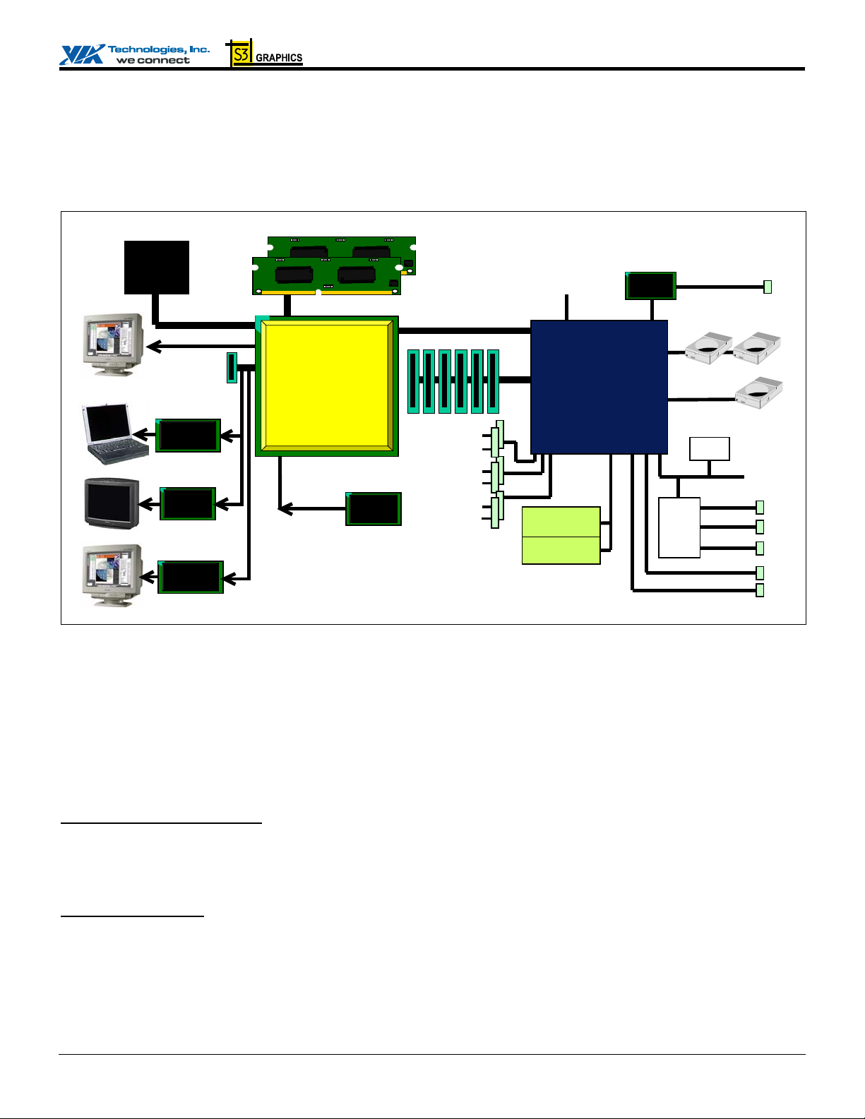
CN400 SYSTEM OVERVIEW
The CN400 is a high performance, cost-effective and energy efficient UMA North Bridge with integrated UniChrome Pro graphics
/ video controller used for the implemen tation of mobile and desktop personal compu ter systems with 200 MHz, 133 MHz or 100
MHz CPU host bus (“Front Side Bus”) based on VIA C3 processors.
CRT
TFT Flat Panel
TV Display
VIA C3
CPU
200 / 133 / 100 MHz
Front Side Bus
RGB, HV, DDC
8x / 4x AGP Slot
FPDP Flat Panel Display Port
24-Bit / Dual 12-B it
Flat P anel Disp lay Inter face
VT1631 LVDS
Transmitt er
Panel
-or-
TV Out
VT1625
TV Encoder
GDVP1 Digital Video Port 1
12-Bit DVI Inter face
VT1632A DVI
Transmitter
DVI Monitor
1.5V
64-Bit DDR400 / 333 / 266 DIMMs
CN400
DDR North Bridge
with UniChrome Pro
Graphics Controller
DVP0
Digital Video Port 0
Video Capture
Vide o
Decoder
66 MHz 8x / 4x V-Link
PCI Slots
6X
USB 2.0
33MHz,
32-bit
PCI
AC'97 Audio Cod ec
System
Management
Bus
VT8237R
V-Link
South Bridge
AC-Link
VT16 16
MC-97
Modem Codec
Integrated
AC'97 Audio
Network
Interface P HY
VT6103
MII
Pri
Sec
LPC
VT1211
Super
10/100 Ethernet
133 / 100 / 66 / 33
EPROM
Serial / IR
Parallel
LPC
Floppy Disk
I/O
Keyboard
Mouse
UDMA / ATA
Figure 1. System Block Diagram
The complete chipset consists of the CN400 North Bridge and the VT8237R V-Link South Bridge. The CN400 integrates VIA’s
most advanced system controller with a high-performance UniChrome Pro 3D / 2D graphics and video controller plus flat panel,
DVI monitor, TV out and Video Capture interfaces. The CN400 provides superior performance between the CPU, DRAM, V-
Link and integrated graphics controller with pipelined, burst and concurrent operation. The VT8237R is a highly integrated
peripheral controller which includes V-Link-to-PCI / V-Link-to-LPC controllers, Ultra DMA IDE controller, USB2.0 host
controller, 10/100Mb networking MAC, AC97 and system power management controllers.
VIA C3 Processor Interface
The CN400 supports 200 / 133 / 100 MHz FSB VIA C3 processors and implements an eight-deep In-Order-Queue. VIA
PowerSaver technology is supported for VIA Antaur processors to reduce system power consumption while sustaining high
processing power.
Memory Controller
The CN400 SDRAM controller supports up to two double-sided DDR400 / 333 / 266 DIMMs for 4 GB maximum physical
memory. The DDR DRAM interface allows zero-wait-state data transfer bursting between the DRAM and the memory
controller’s data buffers. The different banks of D RAM can be compo sed of an arbitrary mixture of 64 / 128 / 256 / 512 / 1024Mb
DRAMs in x8 or x16 configurations. The DRAM controller can run either synchronou s or pseudo- synchrono u s with the host CPU
bus.
Revision 1.18, January 26, 2005 -6- Overview
CN400 Data Sheet
Ultra V-Link
The CN400 North Bridge interfaces to the South Bridge through a high speed (up to 1 GB / Sec) 8x, 66 MHz Data Transfer
interconnect bus called “Ultra V-Link”. Deep pre-fetch and post-write buffers are included to allow for concurrent CPU and VLink operation. The combined CN400 North Bridg e and VT8237R South Bridge system supports enhanced PCI bus commands
such as “Memory-Read-Line”, “Memory-Read-Multiple” and “Memory-Write-Invalid” commands to minimize snoo p overhead.
In addition, advanced features are supported such as CPU write-back forward to PCI master, and CPU write-back merged with PCI
post write buffers to minimize PCI master read latency and DRAM utilization. Delay transaction and read caching mechanisms
are also implemented for further improvement of overall system performance.
System Power Management
For sophisticated power management, the CN400 supports dynamic CKE control to minimize DDR SDRAM power consumption
during normal system state (S0). A separate suspend-well plane is implemented for the memory control logic for the Suspend-toDRAM state. VIA PowerSaver™ Technology is supported to minimize CPU power consumption while sustaining processing
power. The CN400 graphics accelerator implements automatic clock gating for each graphics engine to achieve power saving,
moving to standby or suspend states to further reduce power consumption when idle. Automatic panel power sequencing and
VESA DPMS (Display Power Management Signaling) CRT power-down are supported. Coupled with the VT8237R South
Bridge chip, a complete power conscious PC main board can be implemented with no external glue logic.
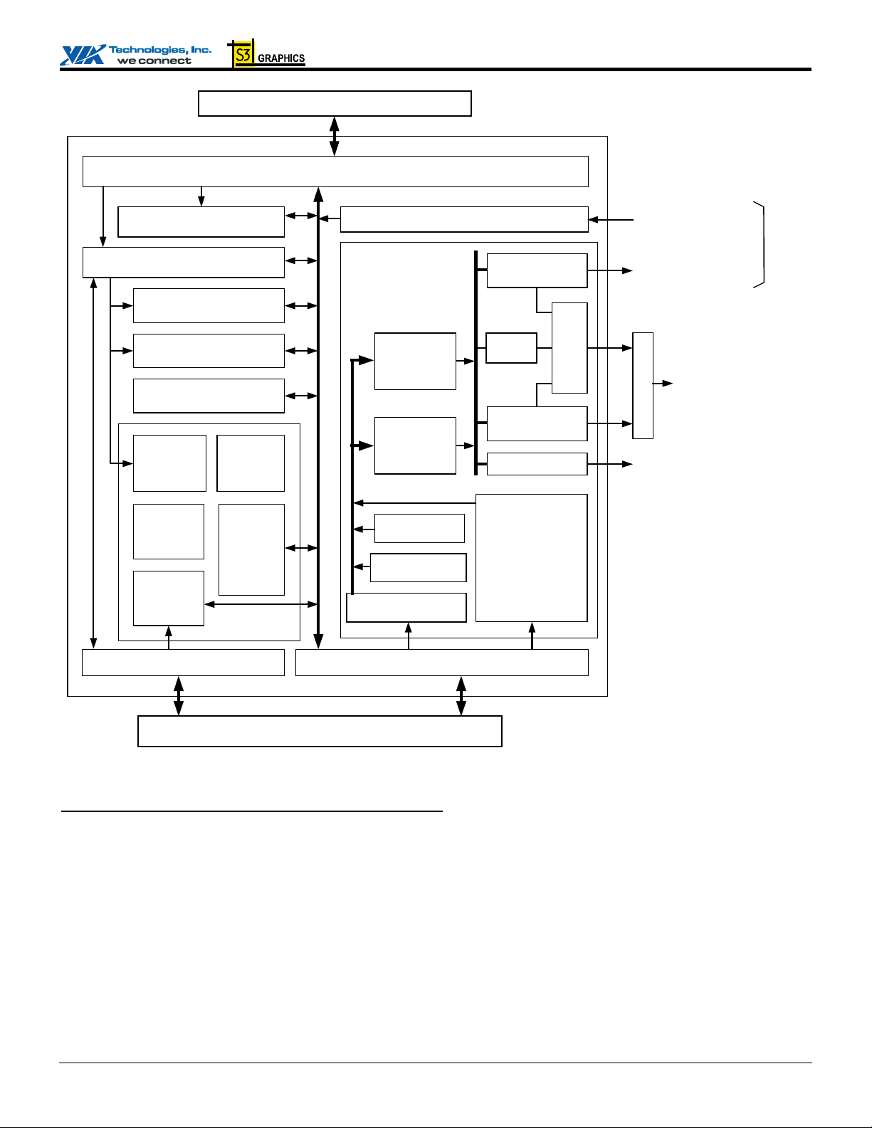
3D Graphics Engine
Featuring an integrated 128-bit 3D graphics engine, the CN400 No rth Bridge utilizes a highly pipelined architecture that prov ides
high performance along with superior image quality. Several new features enhance the 3D architecture, including two pixel
rendering pipes, single-pass multitexturing, bump and cubic mapping, texture comp ression, edge anti-aliasing, vertex fog and fog
table, hardware back-face culling, specular lighting, anisotropic filtering and an 8-bit stencil buffer. The chip also offers the
industry’s only simultaneous usage of single-pass multitexturing and single-cycle trilinear filtering – enabling stunning image
quality without performance loss. Image quality is further enhanced with true 32-b it color ren dering throug hout th e 3D p ipeline to
produce more vivid and realistic images. The advanced triangle setup engine provides industry leading 3D performance for a
realistic user experience in games and other interactive 3D applications. The 3D engine is optimized for AGP texturing from
system memory.
128-bit 2D Graphics Engine
The CN400 North Bridge's advanced 128-bit 2D graphics engine delivers high-speed 2D acceleration for productivity applications.
The enhanced 2D architecture with direct access frame buffer capability optimizes UMA performance and provides acceleration of
all color depths.
MPEG Video Playback
The CN400 North Bridge provides the ideal architecture for high quality MPEG-2 and MPEG-4 based v ideo applications. For
MPEG playback, the integrated video accelerator offloads the CPU by performing planar-to-packed format conversion and motion
video compensation tasks, while the enhanced scaling algorithm delivers incredible full-screen video playback.
Video Capture
The CN400 North Bridge implements an optional Video Capture Port which supports various video capture standards, including
ITU-R BT656, VIP 1.1 and VIP 2.0 and is compliant with the most common video capture format: YUV422. With the integrated
video capture feature, the CN400 can provide high performance video effects for video capturing and playback.
Revision 1.18, January 26, 2005 -7- Overview
CN400 Data Sheet
North Bridge Host Bus
66 MHz PCI Host Bus Interface
VGA GFX Controller
Command Engine
128-bit 2D Engine
MPEG Engine
Video Processor
Vertex
Cache
Setup
Engine
Texture
Engine
Texture
Rendering
Cache
3D Engine
Display
Engine
Capture Port
IGA 1
Digital Video
Port 0
Panel
Digital Video
Port 1
Port
Digital Video
Capture Port
TV Out
24-Bit FPD
plus 12-Bit
Mux
DVP / TVout
Shared
Pins
IGA 2
DAC
CRT
Video Engine
HW Sprite
0/1
(Scaler /
Pipelines
HW Cursor
GFX Stream
YUV-to-RGB)
Video Stream
AGP-like Interface
Memory Interface Unit
North Bridge Memory Controller
Figure 2. Integrated UniChrome Pro Graphics Controller Internal Block Diagram
LCD, DVI Monitor and TV Output Display Support
The CN400 provides three “Digital Video Port” interfaces: FPDP, GDVP1 and DVP0. The Flat Panel Display Port (FPDP)
implements a 24-bit / dual 12-bit interface which is designed to drive a Flat Panel Display via an external LVDS transmitter chip
(such as the VIA VT1631, NSC DS90C387R or Chrontel CH7017) or a TV-Out interf ace to drive a TV display via a TV encod er
(VIA VT1625 using low-voltage 1.5V signal levels). The CN400 can be connected to the external LVDS transmitter chip in either
24-bit or dual-12-bit modes. A wide variety of LCD panels are supported including VGA, SVGA, XGA, SXGA+ and up to
UXGA-resolution TFT color panels, in either SDR (1 pixel / clock) or DDR (2 pixels / clock) modes. UXGA and higher
resolutions require dual-edge data transfer (DDR) mode which is supported by the VIA VT1631 LVDS transmitter chip.
Digital Video Port 0 (DVP0) is normally used for interfacing to a TV encoder, however if DVP0 is used for video capture, Digital
Video Port 1 (GDVP1) may be configured for support of an external TV encoder (VIA VT1625 using low-voltage 1.5V signal
levels). If GDVP1 is not being used for TV out, it can optionally be used to drive a DVI monitor via an external DVI transmitter
chip (such as the VIA VT1632A).
Revision 1.18, January 26, 2005 -8- Overview
CN400 Data Sheet
For High Definition Television application, the CN400 Digital Video Ports can be used to connect to HDTV encoders such as VIA
VT1625 or VT1625M. The VT1625 or VT1625M accepts input from 640x480 to 1024x768 (graphic resolution), 1280x720p,
1920x1080i and 1920x1080p. These encoder s also support various kinds of co mbinations: Composite, S-Video, Compon ent and
RGB outputs display simultaneously with six programmable DACs; and support CGMS-A / Wide Screen Signaling (WSS) /
Closed Captioning, which are for variable clock rates of EIAJ-1204, 1204-1, 1204-2 and EN 300 294.
The flexible display configurations of the CN400 allow support of a flat panel (LVDS interface) or flat panel monitor (DVI
interface), TV display and CRT display at the same time. Internally the CN400 North Bridge provides two separate display
engines, so if two display devices are connected, each can display completely different information at different resolutions, pixel
depths and refresh rates. If more than two display devices are connected, the additional displays must have the same resolution,
pixel depth and refresh rate as one of the first two. The maximum display resolutions supported for one display device are listed in
the table below. If more than one display is implemented (i.e., if both display engines are functioning at the same time), then
available memory bandwidth may limit the display resolutions supported on one o r both displays. This will be dependent on many
factors including primarily clock rates and memory speeds (contact VIA for additional information).
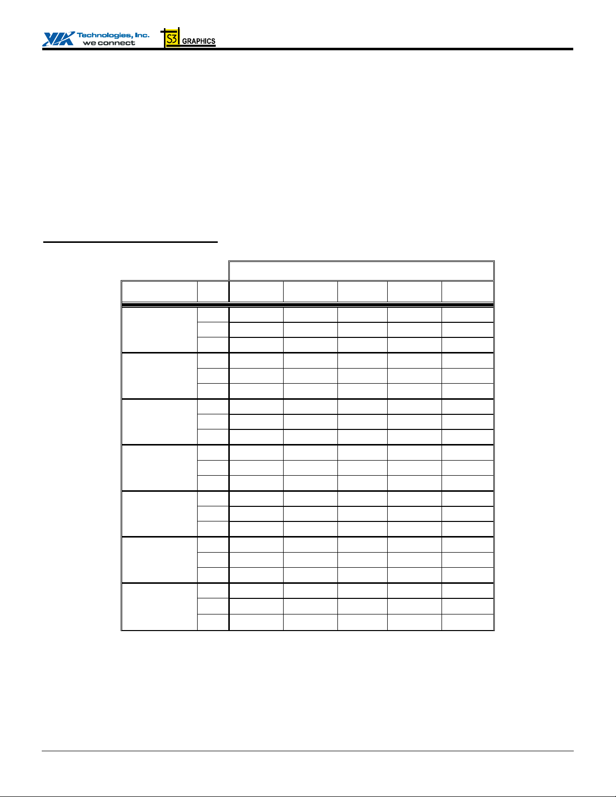
Desktop Modes for Single Display
Resolution BPP 60 75 85 100 120
CRT Maximum Refresh
640x480
800x600
1024x768
1280x1024
1400x1050
1600x1200
1920x1440
8
16
32
8
16
32
8
16
32
8
16
32
8
16
32
8
16
32
8
16
32
√ √ √ √ √
√ √ √ √ √
√ √ √ √ √
√ √ √ √ √
√ √ √ √ √
√ √ √ √ √
√ √ √ √
√ √ √ √
√ √ √ √
√ √ √
√ √ √
√ √ √
√
√
√
√ √ √
√ √ √
√ √1 √2
√ √
√ √
√ √
Table 1. Supported CRT and Panel Screen Resolutions
Key for Desktop Mode
√ = Supported: Mode available and Overlay available
√1 = Supported, but DDR266: Mode available, overlay not available.
√2 = Supported, but DDR266: Mode not available, overlay not available.
Revision 1.18, January 26, 2005 -9- Overview
CN400 Data Sheet
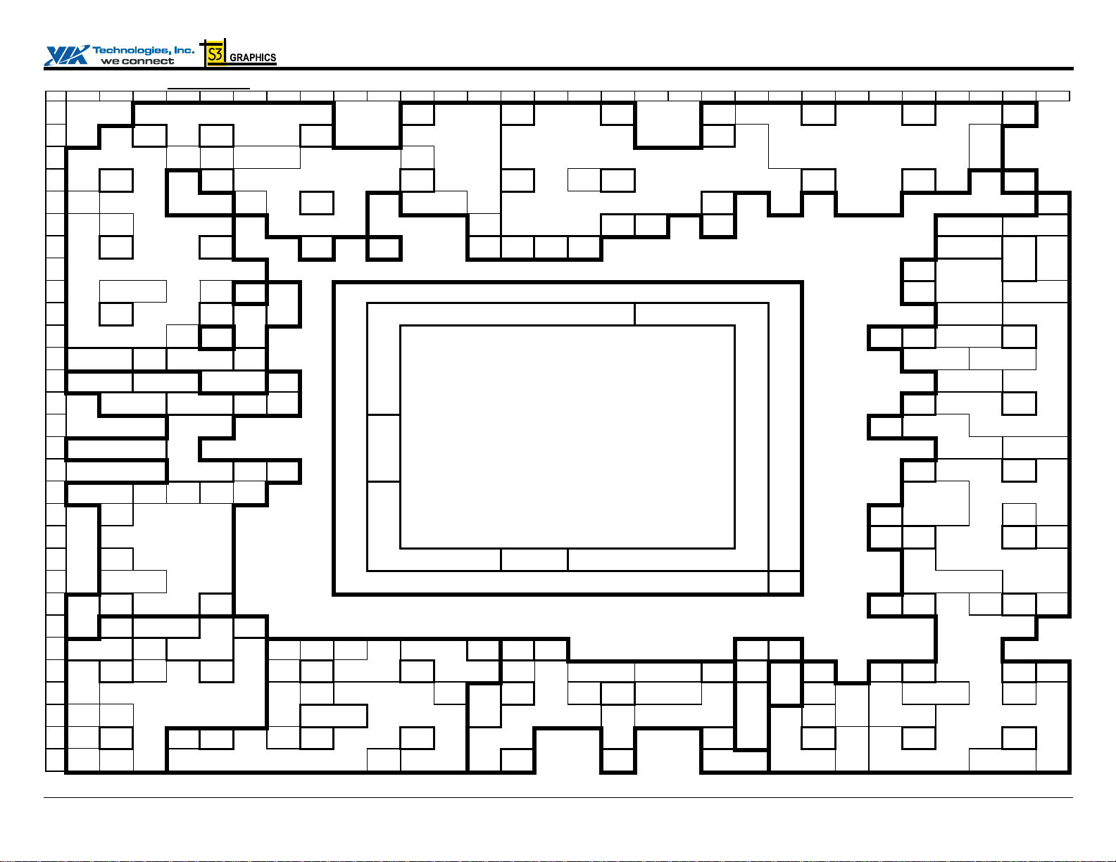
PINOUTS Pin Diagrams Figure 3. Ball Diagram (Top View) – Flat Panel / Digital Video Output Enabled (No External AGP Interface)
Key 1 2 3 4 5 6 7 8 9 10 11 12 13 14 15 16 17 18 19 20 21
HD
HD
HD
HD
HD
A
B
HD
C
43#
HD
D
37#
E NC
HD
F
42#
HD
G
51#
HD
H
63#
HD
J
46#
HD
K
53#
HD
L
62#
V CCA 3 3
M
HCK1
V CCA 1 5
N
PLL3
P
28#
HD
GND
34#
HD
HD
38#
22#
HD
GND
27#
HD
HD
39#
36#
HD
NC
45#
HD
GND
49#
HD
HD
57#
55#
NC NC
HD
GND
54#
HD
HD
56#
61#
GNDA
V CCA 3 3
HCK1
GCK
GNDA
V CCA 1 5
PLL3
PLL1
DISP
DISP
CLKI
CLKO
R
T AB AG AR
U
V
W
Y
AA
AB
AC
AD
AE
COMPP
GDVP1
AF
GDVP1
AG
GDVP1
AH
GDVP1
AJ
GDVP1
AK
H
SYNC V SYNC
DVP0
DET
DVP0
D11
AGP
COMPN
DE
HS
D3
CLK
D8
SP
CLK2
DVP0
HS
GPO 0 DVP0
SP
CLK1
GND
SBDDC
NC
AGP
GDVP1
GND
GDVP1
GDVP1
D2
GDVP1
GDVP1
CLK#
GDVP1
GND
GDVP1
GDVP1
DET
SP
DAT2 R SET
DVP0
D0
DVP0
D2
D3
SP
DAT1
DVP0
D9
DAT
FP
CLK#
VS
D1
D6
D9
D4
29#
25#
26#
HD
31#
NC
GND
NC
HD
44#
HD
41#
HD
59#
HD
52#
HD
58#
NC
V CCA 3 3
HCK2
GNDA
PLL1 H CLK+ H CLK– T CLK
V CCA 1 5
PLL2
V CCA 3 3
DAC1
GNDA
DAC2
V CCA 3 3
DAC2
DVP0
D1
DVP0
D5
DVP0
D7
DVP0
D10
DVP0
DE
SBDDC
CLK
ENA
VDD
GDVP1
D0
GDVP1
D5
GDVP1
D7
FP
DET
FP
D12
HD
GND
24#
HD
NC NC
32#
HD
33#
HD
47#
GND GND
HD
HD
48#
40#
NC
GND
GNDA
HCK2
GNDA
PLL2 G CLK
GNDA
DAC1
GNDA
DAC3
INTA#
DVP0
VS
DVP0
CLK
DVP0
D6
DVP0
D8
GND
ENA
VEE
ENA
BLT
GND NC
NC NC
GDVP1
D10
GND
FP
D15
VREF3
HD
50#
VREF2
HD
60#
GNDA
GCK
XIN
BIST
IN
OUT
DVP0
D4
6 7 AC8 9 10 11 12 13 14 15 16 17 18 19 20 21 22 AC23 24
AGP
VREF1
NC
CLK
GDVP1
D11
FP
D14
FP
D16
HD
13#
HD
20#
HD
30#
HD
7#
GND
HD
HD
11#
12#
HD
HD
14#
18#
HD
NC NC
2#
HD
3#
HD
VREF0
16#
HD
GND
19#
HD
21#
HD
GND
23#
HD
35#
7 H8 9 10 11 12 13 14 15 16 17 18 19 20 21 22 H23 24 25
HD
HD
GP
J
K
L
M
N
P
R
T
U
V
W
Y
AA
AB
VCC
VCC
15
15
VCC
VTT VTT VTT VTT VTT VTT VTT VTT
15
VCC
VTT GND GND GND GND GND GND GND GND GND GND
15
VCC
VTT GND GND GND GND GND GND GND GND GND GND
15
VCC
VTT GND GND GND GND GND GND GND GND GND GND
15
VCC
VTT GND GND GND GND GND GND GND GND GND GND
15
VCC
VCC33
15
GFX
VCC
VCC33
15
GFX
VCC
VCC33
15
GFX
VCC
VCC15
15
AGP
VCC
VCC15
15
AGP
VCC
VCC15
15
AGP
VCC
VCC15
15
AGP
VCC
VCC
15
15
AD
FP
FP
FP
FP
DE
FP
D17
FP
D18
FP
VS
FP
D19
D13
GND
FP1
DE
SBPL
CLK
GND
NC
HS
FP1
CLK#
FP
D23
SBPL
DAT
FP
D21
FP
D00
FP1
VS
FP1
DET
FP
D22
FP
D1
FP
D3
FP1
HS
HD
HD
5#
15#
HD
HD
17#
HD
8#
HD
9#
VCC
15
VCC15
AGP
VCC
15
FP
D20
FP
D7
FP1
CLK
FP
D6
FP
D5
FP
D8
HD
4#
HD
6#
HD
0#
HD
1#
HR
COMP
HD
VREF1
VCC
15
VCC15
AGP
VCC
15
AGP
VREF0
FP
D9 V PAR
NC GND
NC
VD
12
VD
13
10#
NC
GND
VCC
15
GND GND GND GND GND GND GND GND GND GND
GND GND GND GND GND GND GND GND GND GND
GND GND GND GND GND GND GND GND GND GND
GND GND GND GND GND GND GND GND GND GND
GND GND GND GND GND GND GND GND GND GND
GND GND GND GND GND GND GND GND GND GND
VCC15
AGP
VCC
15
FP
D10
GND
FP
D11
FP
D2
GND
FP
D4
HA
GND
NC
HA
29#
GND
HA
26#
HA
18#
HCOMP
VREF
VCC
15
VCC15
VL
VCC
15
VL
COMPP
VD 8 VD 5 VD 0 UP
VD
9
GND GND
HA
23#
HA
30#
HA
27#
HA
20#
HA
24#
HA
17#
GTL
VREF
VCC
15
VCC15
VL
VCC
15
VL
VREF
VD 4 DN
VD 1 V
GND
19#
HA
HA
15#
HA
10#
HA
28#
15
15
GND
HA
HA
13#
3#
HA
HA
12#
5#
HA
NC GND
16#
HA
VREF0
VCC
VCC25
MEM
VCC25
MEM
VCC
VCC
15
15
VCC25
MEM
VCC25
MEM
VCC
15
15
31#
HA
22#
CPU
GND
RST#
HA
21#
HA
GND
25#
GND
VCC
VCC
15
VCC25
VCC25
MEM
MEM
VCC
VCC
15
DN
STB–
GND
STB+
UP
STB–
VD 3 VD
7
DN
UP
CMD
CMD
VD 2 VD 6 VD
GND
STB+
BE#
HA
11#
HA
9#
HA
6#
HA
VREF1
VCC
15
VCC25
MEM
VCC25
MEM
VCC
15
GND
VD
14
11
VD
10
MEM25
22 23 24 25 26 27 28 29
DE
BNR# NC GND
HA
NC
4#
HA
8#
NC
VCC
15
VCC25
MEM
VCC25
MEM
VCC25
MEM
VCC25
MEM
VCC25
MEM
VCC25
MEM
VCC25
MEM
VCC25
MEM
VCC25
MEM
VCC25
MEM
VCC
VCC25
MEM
VCC
15
HREQ
1#
HA
7#
HA
14#
VCC
15
VCC
15
VCC
15
VCC
15
VCC
15
VCC
15
VCC
15
VCC
15
VCC
15
VCC
15
VCC
15
VCC
15
VCC
15
GND
PRI#
HREQ
GND
AA
AB
AD
AGP
MEM
BUSY#
VSUS
15
PWR
OK
RE
SET#
SUS
ST#
VD
15
AE
VREF5
GND
MD
MA
59
MD
GND
63
MD
MD
58
FER#
B
HREQ
2#
NC RS1# RS0#
4#
HREQ
3#
H
E
LOCK#
F
G
GND
J
K
L
M
N
GND
P
R
T
GND
U
V
W
Y
CS
MD
3#
61
MD
13
57
DQS
7#
DQM 7 MD
62
HREQ
0#
HIT
M# D BSY#
HT
RDY#
HIT# GND
VREF0
MEM
VREF1
MEM
VREF2
MEM
VREF3
MA
0
MEM
VREF4
S
WE#
CS
2# S CAS# S RAS#
CS
1#
MD
60
56
D
GND
RDY#
RS2# NC
BREQ
0#
GND NC GND
TEST
IN#
GNDA
MCK
MEM
MD 4 MD
MD 6 MD 2 DQS
CKE 3 CKE 1 MD 3 MD
MD 9 MD
GND
CKE 0 CKE 2 DQM 1 DQS
MA
12
MD
20
MA 9 MA 7 MD
MA 5 MA 8 DQM 2 DQS
MD
19
MA 4 MA 6 MD
MA 2 MA 3 MD
MD
GND
30
MA 1 MD
33
BA 0 BA 1 MA
MD
GND
34
MD
35
MD
40
MD
GND
45
CS
MD
0#
54
MD
GND
50
MD
MD
51
55
30
ADS# GND
NC
DFT
IN# M CLKI M CLKO
V CCA 3
MCK
5
12
MA
11
MD
11
21
MD
22
28
29
MD
26
MD
32
10
DQM
4
MD
39
MD
44
MD
41
MD
46
MD
48
MD
52
DQS
6#
MD
GND
0
MD
GND
1
DQM
0#
0
7
MD
GND
8
MD
1#
13
MD
MD
15
14
MD
GND
10
MD
MD
17
16
2#
MD
GND
18
MD
MD
24
23
DQS
MD
3#
25
DQM
GND
3
MD
MD
31
27
MD
MD
37
36
DQS
GND
4#
MD
38
DQS
GND
5#
DQM 5 MD
42
MD
MD
43
47
MD
GND
49
DQM 6 MD
53
Revision 1.18, January 26, 2005 -10- Pin Diagrams

CN400 Data Sheet
Figure 4. Ball Diagram (Top View) - External AGP Interface Enabled on Display Pins
Key 1 2 3 4 5 6 7 8 9 10 11 12 13 14 15 16 17 18 19 20 21
HD
HD
HD
HD
HD
A
B
HD
C
43#
HD
D
37#
E NC
HD
F
42#
HD
G
51#
HD
H
63#
HD
J
46#
HD
K
53#
HD
L
62#
V CCA 3 3
M
HCK1
V CCA 1 5
N
PLL3
P
28#
HD
GND
34#
HD
HD
38#
22#
HD
GND
27#
HD
HD
39#
36#
HD
NC
45#
HD
GND
49#
HD
HD
57#
55#
NC NC
HD
GND
54#
HD
HD
56#
61#
GNDA
V CCA 3 3
HCK1
GCK
GNDA
V CCA 1 5
PLL3
PLL1
DISP
DISP
CLKI
CLKO
R
T AB AG AR
U
V
W
Y
AA
AB
AC
AD
AE
COMPP
AF
AG
AH
AJ
H
SYNC V SYNC
DVP0
DET
DVP0
D11
AGP
COMPN G WBF
GSBA
1#
GSBA
3#
GSBA
5#
GSBA
6#
SP
DAT2 R SET
SP
DVP0
CLK2
D0
DVP0
DVP0
HS
D2
GPO 0 DVP0
D3
SP
SP
CLK1
DAT1
DVP0
GND
D9
AGP8X
DET# G GNT G REQ
AGP
GSBA
GND
0#
GSB
GSB
STBS
STBF
GSBA
GD29 GD28 GD26
7#
GND GD24
AK GD30 GD31 GD27
29#
25#
26#
HD
31#
NC
GND
NC
HD
44#
HD
41#
HD
59#
HD
52#
HD
58#
NC
V CCA 3 3
HCK2
GNDA
PLL1 H CLK+ H CLK– T CLK
V CCA 1 5
PLL2
V CCA 3 3
DAC1
GNDA
DAC2
V CCA 3 3
DAC2
DVP0
D1
DVP0
D5
DVP0
D7
DVP0
D10
DVP0
DE
GST1 GST2
GSBA
2#
GSBA
4#
GAD
STB1S
GAD
STB1F
HD
GND
24#
HD
NC NC
32#
HD
33#
HD
47#
GND GND
HD
HD
48#
40#
NC
GND
GNDA
HCK2
GNDA
PLL2 G CLK
GNDA
DAC1
GNDA
DAC3
INTA#
DVP0
VS
DVP0
CK
DVP0
D6
DVP0
D8
GND
GST0
GND
GDBIL GD25 GD17
GND GD20
GD23 GD18
VREF3
HD
50#
VREF2
HD
60#
GNDA
GCK
XIN
BIST
IN
OUT
DVP0
D4
6 7 AC8 9 10 11 12 13 14 15 16 17 18 19 20 21 22 AC23 24
AGP
VREF1
G
GD21 GD22
RBF
GDBIH
GD19 GND
GPIPE#
GC#
GD16
BE3
DSEL
GC#
BE2 G TRDY
HD
13#
HD
20#
HD
30#
HD
7#
GND
HD
HD
11#
12#
HD
HD
14#
18#
HD
NC NC
2#
HD
3#
HD
VREF0
16#
HD
GND
19#
HD
21#
HD
GND
23#
HD
35#
7 H8 9 10 11 12 13 14 15 16 17 18 19 20 21 22 H23 24 25
HD
HD
GP
J
K
L
M
N
P
R
T
U
V
W
Y
AA
AB
VCC
VCC
15
15
VCC
VTT VTT VTT VTT VTT VTT VTT VTT
15
VCC
VTT GND GND GND GND GND GND GND GND GND GND
15
VCC
VTT GND GND GND GND GND GND GND GND GND GND
15
VCC
VTT GND GND GND GND GND GND GND GND GND GND
15
VCC
VTT GND GND GND GND GND GND GND GND GND GND
15
VCC
VCC33
15
GFX
VCC
VCC33
15
GFX
VCC
VCC33
15
GFX
VCC
VCC15
15
AGP
VCC
VCC15
15
AGP
VCC
VCC15
15
AGP
VCC
VCC15
15
AGP
VCC
VCC
15
15
AD
G
FRM G PAR
G
GD8 GND GD5 GD3
STOP
G
GD11 GD13 GD1 GD2 NC GND
SERR
G
GC#
GD10
BE1
GC#
BE0
GD12 GD9
G
IRDY
GND GD14
HD
HD
5#
15#
HD
HD
10#
NC
GND
VCC
15
GND GND GND GND GND GND GND GND GND GND
GND GND GND GND GND GND GND GND GND GND
GND GND GND GND GND GND GND GND GND GND
GND GND GND GND GND GND GND GND GND GND
GND GND GND GND GND GND GND GND GND GND
GND GND GND GND GND GND GND GND GND GND
VCC15
AGP
VCC
15
GD0 GD15
GAD
STB0S
GND GD7
GAD
STB0F
HD
17#
4#
HD
HD
8#
6#
HD
HD
9#
0#
HD
1#
HR
COMP
HD
VREF1
VCC
VCC
15
15
VCC15
VCC15
AGP
AGP
VCC
VCC
15
15
AGP
VREF0
GD6 NC
VD
12
VD
GD4
13
HA
GND
NC
HA
29#
GND
HA
26#
HA
18#
HCOMP
VREF
VCC
15
VCC15
VL
VCC
15
VL
COMPP
V
PAR
VD 8 VD 5 VD 0 UP
VD
9
GND GND
HA
23#
HA
30#
HA
27#
HA
20#
HA
24#
HA
17#
GTL
VREF
VCC
15
VCC15
VL
VCC
15
VL
VREF
VD 4 DN
VD 1 V
GND
19#
HA
HA
15#
HA
10#
HA
28#
15
15
GND
HA
HA
13#
3#
HA
HA
12#
5#
HA
NC GND
16#
HA
VREF0
VCC
VCC25
MEM
VCC25
MEM
VCC
VCC
15
15
VCC25
MEM
VCC25
MEM
VCC
15
15
31#
HA
22#
CPU
GND
RST#
HA
21#
HA
GND
25#
GND
VCC
VCC
15
VCC25
VCC25
MEM
MEM
VCC
VCC
15
DN
STB–
GND
STB+
UP
STB–
VD 3 VD
7
DN
UP
CMD
CMD
VD 2 VD 6 VD
GND
STB+
BE#
HA
11#
HA
9#
HA
6#
HA
VREF1
VCC
15
VCC25
MEM
VCC25
MEM
VCC
15
GND
VD
14
11
VD
10
22 23 24 25 26 27 28 29
DE
BNR# NC GND
HA
NC
4#
HA
8#
NC
VCC
15
VCC25
MEM
VCC25
MEM
VCC25
MEM
VCC25
MEM
VCC25
MEM
VCC25
MEM
VCC25
MEM
VCC25
MEM
VCC25
MEM
VCC25
MEM
VCC25
MEM
VCC25
MEM
VCC
15
HREQ
1#
HA
7#
HA
14#
VCC
15
VCC
15
VCC
15
VCC
15
VCC
15
VCC
15
VCC
15
VCC
15
VCC
15
VCC
15
VCC
15
VCC
15
VCC
15
GND
PRI#
HREQ
GND
AA
AB
AD
AGP
MEM
BUSY#
VSUS
15
PWR
OK
RE
SET#
SUS
ST#
VD
15
AE
VREF5
GND
MD
MA
59
MD
GND
63
MD
MD
58
FER#
B
HREQ
2#
NC RS1# RS0#
4#
HREQ
3#
H
E
LOCK#
F
G
GND
J
K
L
M
N
GND
P
R
T
GND
U
V
W
Y
CS
MD
3#
61
MD
13
57
DQS
7#
DQM 7 MD
62
HREQ
0#
HIT
M# D BSY#
HT
RDY#
HIT# GND
VREF0
MEM
VREF1
MEM
VREF2
MEM
VREF3
MA
0
MEM
VREF4
S
WE#
CS
2# S CAS# S RAS#
CS
1#
MD
60
56
D
GND
RDY#
RS2# NC
BREQ
0#
GND NC GND
TEST
IN#
GNDA
MCK
MEM
MD 4 MD
MD 6 MD 2 DQS
CKE 3 CKE 1 MD 3 MD
MD 9 MD
GND
CKE 0 CKE 2 DQM 1 DQS
MA
12
MD
20
MA 9 MA 7 MD
MA 5 MA 8 DQM 2 DQS
MD
19
MA 4 MA 6 MD
MA 2 MA 3 MD
MD
GND
30
MA 1 MD
33
BA 0 BA 1 MA
MD
GND
34
MD
35
MD
40
MD
GND
45
CS
MD
0#
54
MD
GND
50
MD
MD
51
55
30
ADS# GND
NC
DFT
IN# M CLKI M CLKO
V CCA 3 3
MCK
5
12
MA
11
MD
11
21
MD
22
28
29
MD
26
MD
32
10
DQM
4
MD
39
MD
44
MD
41
MD
46
MD
48
MD
52
DQS
6#
MD
GND
0
MD
GND
1
DQM
0#
0
7
MD
GND
8
MD
1#
13
MD
MD
15
14
MD
GND
10
MD
MD
17
16
2#
MD
GND
18
MD
MD
24
23
DQS
MD
3#
25
DQM
GND
3
MD
MD
31
27
MD
MD
37
36
DQS
GND
4#
MD
38
DQS
GND
5#
DQM 5 MD
42
MD
MD
43
47
MD
GND
49
DQM 6 MD
53
Revision 1.18, January 26, 2005 -11- Pin Diagrams
CN400 Data Sheet
Pin Lists
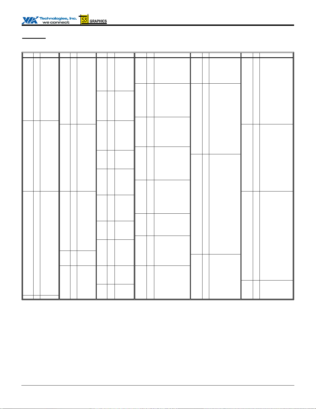
Table 2. Pin List (Listed by Pin Number) – Display Interface Enabled (No External AGP)
Pin # Pin Name Pin # Pin Name Pin # Pin Name Pin # Pin Name Pin # Pin Name Pin # Pin Name
A03 IO HD28# D03 IO HD27# J01 IO HD46# V05 O INTA# AE10 O FP1VS AH13 – NC
A04 IO HD29# D06 IO HD33# J02 – NC V06 O DVP0D04 / TVD04 AE11 O FPD10 AH14 IO VD08
A05 IO HD25# D07 IO HD21# J03 – NC V26 O MA04 AE12 O FPD20 /GTV0D08 AH15 IO VD05
A06 IO HD26# D08 IO HD30# J04 IO HD52# V27 O MA06 AE14 AI VLCOMPP AH16 IO VD00
A07 IO HD16# D09 IO HD14# J05 – NC V28 IO MD28 AE21 O AGPBUSY# / NMI AH17 I UPSTB+
A08 IO HD13# D10 IO HD18# J27 IO MD06 V29 IO MD24 AE27 IO MD40 AH18 IO VD02
A12 IO HD05# D12 IO HD09# J28 IO MD02 V30 IO MD23 AE28 IO MD44 AH19 IO VD06
A13 IO HD15# D13 IO HD00# J29 IO DQS0# W02 IO SPCLK2 AF01 O GDVP1DE AH20 IO VD11
A15 IO HA23# D15 IO HA20# J30 O DQM0 W03 O DVP0D00 / TVD00 AF03 O GDVP1VS AH21 I RESET#
A16 IO HA19# D16 O CPURST# K01 IO HD53# W04 O DVP0D01 / TVD01 AF04 O GDVP1D00 AH22 IO MD59
A20 IO HA11# D18 IO HA12# K03 IO HD54# W05 O DVP0VS / TVVS AF06 – NC AH23 O MA13
A21 IO BNR# D19 IO HA05# K04 IO HD58# W26 O MA02 AF07 O FPDE / GTV0DE AH24 IO MD57
A22 – NC D20 IO HA06# K06 IO HD50# W27 O MA03 AF09 O FP1CLK# AH25 O CS1#
A24 IO DEFER# D21 – NC K27 O CKE3 W28 IO MD29 AF10 I FP1DET AH26 O CS0#
A25 IO HREQ0# D22 IO HA07# K28 O CKE1 W29 IO DQS3# AF12 O FPD07 AH27 IO MD54
A27 IO DRDY# D24 IO HREQ3# K29 IO MD03 W30 IO MD25 AF13 O FPD09 AH28 IO MD48
A28 IO ADS# D25 IO HTRDY# K30 IO MD07 Y02 O DVP0HS / TVHS AF14 IO VPAR AH29 IO MD43
B02 IO HD34# D27 – NC L01 IO HD62# Y03 O DVP0D02 / TVD02 AF15 IO VD04 AH30 IO MD47
B04 IO HD31# E01 – NC L02 IO HD56# Y04 O DVP0D05 / TVD05 AF16 O DNSTB+ AJ01 O GDVP1CLK
B06 IO HD24# E02 IO HD39# L03 IO HD61# Y05 O DVP0CLK / TVCLK AF17 O DNSTB– AJ03 O GDVP1D09
B07 IO HD19# E03 IO HD36# L04 – NC Y25 O MA00 AF18 IO VD03 AJ04 I FPDET /GTVCLKIN
B11 IO HD10# E06 – NC L06 IO HD60# Y27 IO MD30 AF19 IO VD07 AJ06 O FPD14 / GTV0D02
B12 IO HD17# E07 IO HD23# L27 IO MD09 Y28 IO MD26 AF25 O SWE# AJ07 O FPVS / GTV0VS
B13 IO HD04# E09 IO HD02# L28 IO MD12 Y30 O DQM3 AF27 IO MD45 AJ09 O FPD21 / GTV0D09
B14 – NC E11 – NC L30 IO MD08 AA02 O GPO0 AF28 IO MD41 AJ10 O FPD03
B15 IO HA30# E12 – NC M26 O CKE0 AA03 O DVP0D03 / TVD03 AF30 IO DQS5# AJ12 O FPD05
B16 IO HA31# E13 IO HD01# M27 O CKE2 AA04 O DVP0D07 / TVD07 AG01 O GDVP1HS AJ13 IO VD12
B17 IO HA15# E14 IO HA26# M28 O DQM1 AA05 O DVP0D06 / TVD06 AG02 O GDVP1D02 AJ14 IO VD09
B21 IO HA04# E15 IO HA24# M29 IO DQS1# AA26 O MA01 AG03 O GDVP1D01 AJ17 I UPSTB–
B22 – NC E16 IO HA21# M30 IO MD13 AA27 IO MD33 AG04 O GDVP1D05 AJ21 I SUSST#
B23 IO BPRI# E17 IO HA28# N05 I HCLK+ AA28 IO MD32 AG05 – NC AJ22 IO MD63
B24 IO HREQ2# E18 IO HA16# N06 I HCLK– AA29 IO MD31 AG06 – NC AJ24 IO DQS7#
B25 I HITM# E19 – NC N07 I TCLK AA30 IO MD27 AG07 O FPD17/GTV0D05 AJ25 IO MD60
B26 IO DBSY# E22 IO HA14# N27 O MA12 AB02 IO SPCLK1 AG08 O FP1DE AJ27 IO MD50
B27 IO RS2# E24 I HLOCK# N28 O MA11 AB03 IO SPDAT1 AG09 O FPD23/GTV0D11 AJ28 IO MD52
B28 – NC E25 IO HIT# N29 IO MD15 AB04 O DVP0D10 / TVD10 AG10 O FPD22/GTV0D10 AJ30 IO MD49
C01 IO HD43# F01 IO HD42# N30 IO MD14 AB05 O DVP0D08 / TVD08 AG11 O FPD11 AK01 O GDVP1D08
C02 IO HD38# F02 – NC P02 I DISPCLKI AB26 O BA0 AG12 O FP1CLK AK02 I GDVP1DET
C03 IO HD22# F03 IO HD45# P03 O DISPCLKO AB27 O BA1 AG13 – NC AK03 O GDVP1D04
C04 – NC F04 IO HD44# P06 I GCLK AB28 O MA10 AG15 IO VD01 AK04 O FPD12 / GTV0D00
C05 IO HD32# F05 IO HD47# P07 I XIN AB29 IO MD37 AG16 IO VBE# AK05 O FPD15 / GTV0D03
C06 – NC F07 IO HD35# P27 IO MD20 AB30 IO MD36 AG18 O DNCMD AK06 O FPD16 / GTV0D04
C07 – NC F08 IO HD07# P28 IO MD11 AC01 I DVP0DET/TVCKIN AG19 I UPCMD AK07 O FPD19 / GTV0D07
C08 IO HD20# F09 IO HD03# P30 IO MD10 AC03 O DVP0D09 / TVD09 AG20 IO VD14 AK08 – NC
C09 IO HD11# F13 AI HRCOMP R26 O MA09 AC04 O DVP0DE / TVDE AG21 I PWROK AK09 O FPD00
C10 IO HD12# F14 IO HA18# R27 O MA07 AC27 IO MD34 AG23 O CS3# AK10 O FP1HS
C11 – NC F15 IO HA17# R28 IO MD21 AC28 O DQM4 AG24 IO MD61 AK11 O FPD04
C12 IO HD08# F16 IO HA25# R29 IO MD17 AC30 IO DQS4# AG25 O CS2# AK12 O FPD08
C13 IO HD06# F27 I TESTIN# R30 IO MD16 AD01 O DVP0D11 /TVD11 AG26 O SCAS# AK13 IO VD13
C14 IO HA29# F28 I DFTIN# T01 AO AB AD02 – NC AG27 O SRAS# AK20 IO VD10
C15 IO HA27# F29 I MCLKI T02 AO AG AD03 IO SBDDCDAT AG28 IO MD46 AK21 IO VD15
C16 IO HA22# F30 O MCLKO T03 AO AR AD04 IO SBDDCCLK AG29 O DQM5 AK22 IO MD58
C17 IO HA10# G01 IO HD51# T27 O MA05 AD05 O ENAVEE AG30 IO MD42 AK23 IO MD62
C18 IO HA13# G03 IO HD49# T28 O MA08 AD27 IO MD35 AH01 O GDVP1D03 AK24 O DQM7
C19 IO HA03# G04 IO HD41# T29 O DQM2 AD28 IO MD39 AH02 O GDVP1CLK# AK25 IO MD56
C20 IO HA09# G30 IO MD00 T30 IO DQS2# AD29 IO MD38 AH03 O GDVP1D06 AK26 IO MD51
C21 IO HA08# H01 IO HD63# U06 I BISTIN AE01 AI AGPPCMP AH04 O GDVP1D07 AK27 IO MD55
C22 IO HREQ1# H02 IO HD57# U07 O GPOUT AE02 AI AGPNCMP AH05 O GDVP1D10 AK28 IO DQS6#
C23 IO HREQ4# H03 IO HD55# U27 IO MD19 AE03 O FPCLK#/GTV0CK# AH06 O GDVP1D11 AK29 O DQM6
C24 – NC H04 IO HD59# U28 IO MD22 AE04 O ENAVDD AH07 O FPD18/GTV0D06 AK30 IO MD53
C25 IO RS1# H05 IO HD48# U30 IO MD18 AE05 O ENABLT AH08 IO SBPLCLK
C26 IO RS0# H06 IO HD40# V01 O HSYNC AE06 – NC AH09 IO SBPLDAT
C27 O BREQ0# H27 IO MD04 V02 O VSYNC AE07 O FPCLK/GTV0CLK AH10 O FPD01
C28 – NC H28 IO MD05 V03 IO SPDAT2 AE08 O FPD13 /GTV0D01 AH11 O FPD02
D01 IO HD37# H30 IO MD01 V04 AI RSET AE09 O FPHS /GTV0HS AH12 O FPD06
Revision 1.18, January 26, 2005 -12- Pin Lists
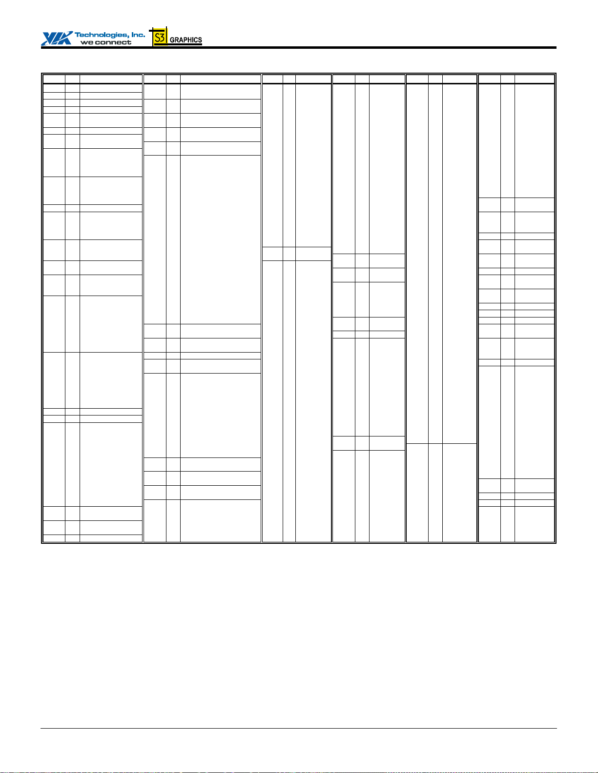
CN400 Data Sheet
Table 3. Pin List (Listed by Pin Name) - Display Interface Enabled (No External AGP)
Pin # Pin Name Pin # Pin Name Pin # Pin Name Pin # Pin Name Pin # Pin Name Pin # Pin Name
T01 AO AB AE04 O ENAVDD C20 IO HA09# H06 IO HD40# M30 IO MD13 E11 – NC
A28 IO ADS# AD05 O ENAVEE C17 IO HA10# G04 IO HD41# N30 IO MD14 E12 – NC
T02 AO AG AG12 O FP1CLK A20 IO HA11# F01 IO HD42# N29 IO MD15 E19 – NC
AE21 O AGPBUSY# / NMI AF09 O FP1CLK# D18 IO HA12# C01 IO HD43# R30 IO MD16 F02 – NC
AE02 AI AGPCOMPN AG08 O FP1DE C18 IO HA13# F04 IO HD44# R29 IO MD17 J02 – NC
AE01 AI AGPCOMPP AF10 I FP1DET E22 IO HA14# F03 IO HD45# U30 IO MD18 J03 – NC
T03 AO AR AK10 O FP1HS B17 IO HA15# J01 IO HD46# U27 IO MD19 J05 – NC
AB26 O BA0 AE10 O FP1VS E18 IO HA16# F05 IO HD47# P27 IO MD20 L04 – NC
AB27 O BA1 AE07 O FPCLK / GTV0CLK F15 IO HA17# H05 IO HD48# R28 IO MD21 AD02 – NC
U06 I BISTIN AE03 O FPCLK#/GTV0CLK# F14 IO HA18# G03 IO HD49# U28 IO MD22 AE06 – NC
A21 IO BNR# AK09 O FPD00 A16 IO HA19# K06 IO HD50# V30 IO MD23 AF06 – NC
B23 IO BPRI# AH10 O FPD01 D15 IO HA20# G01 IO HD51# V29 IO MD24 AG05 – NC
C27 O BREQ0# AH11 O FPD02 E16 IO HA21# J04 IO HD52# W30 IO MD25 AG06 – NC
M26 O CKE0 AJ10 O FPD03 C16 IO HA22# K01 IO HD53# Y28 IO MD26 AG13 – NC
K28 O CKE1 AK11 O FPD04 A15 IO HA23# K03 IO HD54# AA30 IO MD27 AH13 – NC
M27 O CKE2 AJ12 O FPD05 E15 IO HA24# H03 IO HD55# V28 IO MD28 AK08 – NC
K27 O CKE3 AH12 O FPD06 F16 IO HA25# L02 IO HD56# W28 IO MD29 AG21 I PWROK
D16 O CPURST# AF12 O FPD07 E14 IO HA26# H02 IO HD57# Y27 IO MD30 AH21 I RESET#
AH26 O CS0# AK12 O FPD08 C15 IO HA27# K04 IO HD58# AA29 IO MD31 C26 IO RS0#
AH25 O CS1# AF13 O FPD09 E17 IO HA28# H04 IO HD59# AA28 IO MD32 C25 IO RS1#
AG25 O CS2# AE11 O FPD10 C14 IO HA29# L06 IO HD60# AA27 IO MD33 B27 IO RS2#
AG23 O CS3# AG11 O FPD11 B15 IO HA30# L03 IO HD61# AC27 IO MD34 V04 AI RSET
B26 IO DBSY# AK04 O FPD12 / GTV0D00 B16 IO HA31# L01 IO HD62# AD27 IO MD35 AD03 IO SBDDCDAT
A24 IO DEFER# AE08 O FPD13 / GTV0D01 N05 I HCLK+ H01 IO HD63# AB30 IO MD36 AD04 IO SBDDCCLK
F28 I DFTIN# AJ06 O FPD14 / GTV0D02 N06 I HCLK– E25 IO HIT# AB29 IO MD37 AH08 IO SBPLCLK
P02 I DISPCLKI AK05 O FPD15 / GTV0D03 D13 IO HD00# B25 I HITM# AD29 IO MD38 AH09 IO SBPLDAT
P03 O DISPCLKO AK06 O FPD16 / GTV0D04 E13 IO HD01# E24 I HLOCK# AD28 IO MD39 AG26 O SCAS#
AG18 O DNCMD AG07 O FPD17 / GTV0D05 E09 IO HD02# F13 AI HRCOMP AE27 IO MD40 AB02 IO SPCLK1
AF16 O DNSTB+ AH07 O FPD18 / GTV0D06 F09 IO HD03# A25 IO HREQ0# AF28 IO MD41 W02 IO SPCLK2
AF17 O DNSTB– AK07 O FPD19 / GTV0D07 B13 IO HD04# C22 IO HREQ1# AG30 IO MD42 AB03 IO SPDAT1
J30 O DQM0 AE12 O FPD20 / GTV0D08 A12 IO HD05# B24 IO HREQ2# AH29 IO MD43 V03 IO SPDAT2
M28 O DQM1 AJ09 O FPD21 / GTV0D09 C13 IO HD06# D24 IO HREQ3# AE28 IO MD44 AG27 O SRAS#
T29 O DQM2 AG10 O FPD22 / GTV0D10 F08 IO HD07# C23 IO HREQ4# AF27 IO MD45 AJ21 I SUSST#
Y30 O DQM3 AG09 O FPD23 / GTV0D11 C12 IO HD08# V01 O HSYNC AG28 IO MD46 AF25 O SWE#
AC28 O DQM4 AF07 O FPDE / GTV0DE D12 IO HD09# D25 IO HTRDY# AH30 IO MD47 N07 I TCLK
AG29 O DQM5 AJ04 I FPDET / GTVCLKIN B11 IO HD10# V05 O INTA# AH28 IO MD48 F27 I TESTIN#
AK29 O DQM6 AE09 O FPHS / GTV0HS C09 IO HD11# Y25 O MA00 AJ30 IO MD49 AG19 I UPCMD
AK24 O DQM7 AJ07 O FPVS / GTV0VS C10 IO HD12# AA26 O MA01 AJ27 IO MD50 AH17 I UPSTB+
J29 IO DQS0# P06 I GCLK A08 IO HD13# W26 O MA02 AK26 IO MD51 AJ17 I UPSTB–
M29 IO DQS1# AJ01 O GDVP1CLK / GTV1CLK D09 IO HD14# W27 O MA03 AJ28 IO MD52 AG16 IO VBE#
T30 IO DQS2# AH02 O GDVP1CLK#/GTV1CLK# A13 IO HD15# V26 O MA04 AK30 IO MD53 AH16 IO VD00
W29 IO DQS3# AF04 O GDVP1D00 / GTV1D00 A07 IO HD16# T27 O MA05 AH27 IO MD54 AG15 IO VD01
AC30 IO DQS4# AG03 O GDVP1D01 / GTV1D01 B12 IO HD17# V27 O MA06 AK27 IO MD55 AH18 IO VD02
AF30 IO DQS5# AG02 O GDVP1D02 / GTV1D02 D10 IO HD18# R27 O MA07 AK25 IO MD56 AF18 IO VD03
AK28 IO DQS6# AH01 O GDVP1D03 / GTV1D03 B07 IO HD19# T28 O MA08 AH24 IO MD57 AF15 IO VD04
AJ24 IO DQS7# AK03 O GDVP1D04 / GTV1D04 C08 IO HD20# R26 O MA09 AK22 IO MD58 AH15 IO VD05
A27 IO DRDY# AG04 O GDVP1D05 / GTV1D05 D07 IO HD21# AB28 O MA10 AH22 IO MD59 AH19 IO VD06
Y05 O DVP0CLK / TVCLK AH03 O GDVP1D06 / GTV1D06 C03 IO HD22# N28 O MA11 AJ25 IO MD60 AF19 IO VD07
W03 O DVP0D00 / TVD00 AH04 O GDVP1D07 / GTV1D07 E07 IO HD23# N27 O MA12 AG24 IO MD61 AH14 IO VD08
W04 O DVP0D01 / TVD01 AK01 O GDVP1D08 / GTV1D08 B06 IO HD24# AH23 O MA13 AK23 IO MD62 AJ14 IO VD09
Y03 O DVP0D02 / TVD02 AJ03 O GDVP1D09 / GTV1D09 A05 IO HD25# F29 I MCLKI AJ22 IO MD63 AK20 IO VD10
AA03 O DVP0D03 / TVD03 AH05 O GDVP1D10 / GTV1D10 A06 IO HD26# F30 O MCLKO A22 – NC AH20 IO VD11
V06 O DVP0D04 / TVD04 AH06 O GDVP1D11 / GTV1D11 D03 IO HD27# G30 IO MD00 B14 – NC AJ13 IO VD12
Y04 O DVP0D05 / TVD05 AF01 O GDVP1DE / GTV1DE A03 IO HD28# H30 IO MD01 B22 – NC AK13 IO VD13
AA05 O DVP0D06 / TVD06 AK02 I GDVP1DET A04 IO HD29# J28 IO MD02 B28 – NC AG20 IO VD14
AA04 O DVP0D07 / TVD07 AG01 O GDVP1HS / GTV1HS D08 IO HD30# K29 IO MD03 C04 – NC AK21 IO VD15
AB05 O DVP0D08 / TVD08 AF03 O GDVP1VS / GTV1VS B04 IO HD31# H27 IO MD04 C06 – NC AE14 AI VLCOMPP
AC03 O DVP0D09 / TVD09 AA02 O GPO0 C05 IO HD32# H28 IO MD05 C07 – NC AF14 IO VPAR
AB04 O DVP0D10 / TVD10 U07 O GPOUT D06 IO HD33# J27 IO MD06 C11 – NC V02 O VSYNC
AD01 O DVP0D11 / TVD11 C19 IO HA03# B02 IO HD34# K30 IO MD07 C24 – NC P07 I XIN
AC04 O DVP0DE / TVDE B21 IO HA04# F07 IO HD35# L30 IO MD08 C28 – NC
AC01 I DVP0DET / TVCKI D19 IO HA05# E03 IO HD36# L27 IO MD09 D21 – NC
Y02 O DVP0HS / TVHS D20 IO HA06# D01 IO HD37# P30 IO MD10 D27 – NC
W05 O DVP0VS / TVVS D22 IO HA07# C02 IO HD38# P28 IO MD11 E01 – NC
AE05 O ENABLT C21 IO HA08# E02 IO HD39# L28 IO MD12 E06 – NC
Revision 1.18, January 26, 2005 -13- Pin Lists
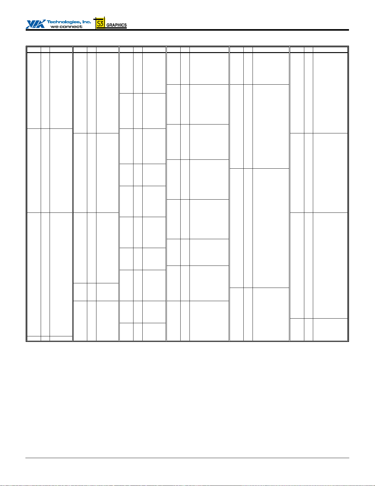
CN400 Data Sheet
Table 4. Pin List (Listed by Pin Number) - External AGP Interface Enabled (No Panel Interface)
Pin # Pin Name Pin # Pin Name Pin # Pin Name Pin # Pin Name Pin # Pin Name Pin # Pin Name
A03 IO HD28# D03 IO HD27# J01 IO HD46# V05 O INTA# AE10 IO GPAR AH13 – NC
A04 IO HD29# D06 IO HD33# J02 – NC V06 O DVP0D04 / TVD04 AE11 IO GD0 AH14 IO VD08
A05 IO HD25# D07 IO HD21# J03 – NC V26 O MA04 AE12 IO GD15 AH15 IO VD05
A06 IO HD26# D08 IO HD30# J04 IO HD52# V27 O MA06 AE14 AI VLCOMPP AH16 IO VD00
A07 IO HD16# D09 IO HD14# J05 – NC V28 IO MD28 AE21 O AGPBUSY# / NMI AH17 I UPSTB+
A08 IO HD13# D10 IO HD18# J27 IO MD06 V29 IO MD24 AE27 IO MD40 AH18 IO VD02
A12 IO HD05# D12 IO HD09# J28 IO MD02 V30 IO MD23 AE28 IO MD44 AH19 IO VD06
A13 IO HD15# D13 IO HD00# J29 IO DQS0# W02 IO SPCLK2 AF01 I GSBA1# AH20 IO VD11
A15 IO HA23# D15 IO HA20# J30 O DQM0 W03 O DVP0D00 / TVD00 AF03 I GSBA0# AH21 I RESET#
A16 IO HA19# D16 O CPURST# K01 IO HD53# W04 O DVP0D01 / TVD01 AF04 I GSBA2# AH22 IO MD59
A20 IO HA11# D18 IO HA12# K03 IO HD54# W05 O DVP0VS / TVVS AF06 IO GDBIH / GPIPE# AH23 O MA13
A21 IO BNR# D19 IO HA05# K04 IO HD58# W26 O MA02 AF07 IO GD19 AH24 IO MD57
A22 – NC D20 IO HA06# K06 IO HD50# W27 O MA03 AF09 IO GSTOP AH25 O CS1#
A24 IO DEFER# D21 – NC K27 O CKE3 W28 IO MD29 AF10 IO GD8 AH26 O CS0#
A25 IO HREQ0# D22 IO HA07# K28 O CKE1 W29 IO DQS3# AF12 IO GD5 AH27 IO MD54
A27 IO DRDY# D24 IO HREQ3# K29 IO MD03 W30 IO MD25 AF13 IO GD3 AH28 IO MD48
A28 IO ADS# D25 IO HTRDY# K30 IO MD07 Y02 O DVP0HS / TVHS AF14 IO VPAR AH29 IO MD43
B02 IO HD34# D27 – NC L01 IO HD62# Y03 O DVP0D02 / TVD02 AF15 IO VD04 AH30 IO MD47
B04 IO HD31# E01 – NC L02 IO HD56# Y04 O DVP0D05 / TVD05 AF16 O DNSTB+
B06 IO HD24# E02 IO HD39# L03 IO HD61# Y05 O DVP0CK / TVCK AF17 O DNSTB– AJ03 IO GD24
B07 IO HD19# E03 IO HD36# L04 – NC Y25 O MA00 AF18 IO VD03 AJ04 IO GADSTB1S
B11 IO HD10# E06 – NC L06 IO HD60# Y27 IO MD30 AF19 IO VD07 AJ06 IO GD20
B12 IO HD17# E07 IO HD23# L27 IO MD09 Y28 IO MD26 AF25 O SWE# AJ07 IO GDEVSEL
B13 IO HD04# E09 IO HD02# L28 IO MD12 Y30 O DQM3 AF27 IO MD45 AJ09 IO GD14
B14 – NC E11 – NC L30 IO MD08 AA02 O GPO0 AF28 IO MD41 AJ10 IO GC#BE0
B15 IO HA30# E12 – NC M26 O CKE0 AA03 O DVP0D03 / TVD03 AF30 IO DQS5# AJ12 IO GD7
B16 IO HA31# E13 IO HD01# M27 O CKE2 AA04 O DVP0D07 / TVD07 AG01 I GSBA3# AJ13 IO VD12
B17 IO HA15# E14 IO HA26# M28 O DQM1 AA05 O DVP0D06 / TVD06 AG02 I GSBSTBS AJ14 IO VD09
B21 IO HA04# E15 IO HA24# M29 IO DQS1# AA26 O MA01 AG03 I GSBSTBF AJ17 I UPSTB–
B22 – NC E16 IO HA21# M30 IO MD13 AA27 IO MD33 AG04 I GSBA4# AJ21 I SUSST#
B23 IO BPRI# E17 IO HA28# N05 I HCLK+ AA28 IO MD32 AG05 IO GDBIL AJ22 IO MD63
B24 IO HREQ2# E18 IO HA16# N06 I HCLK– AA29 IO MD31 AG06 IO GD25 AJ24 IO DQS7#
B25 I HITM# E19 – NC N07 I TCLK AA30 IO MD27 AG07 IO GD17 AJ25 IO MD60
B26 IO DBSY# E22 IO HA14# N27 O MA12 AB02 IO SPCLK1 AG08 IO GSERR AJ27 IO MD50
B27 IO RS2# E24 I HLOCK# N28 O MA11 AB03 IO SPDAT1 AG09 IO GD11 AJ28 IO MD52
B28 – NC E25 IO HIT# N29 IO MD15 AB04 O DVP0D10 / TVD10 AG10 IO GD13 AJ30 IO MD49
C01 IO HD43# F01 IO HD42# N30 IO MD14 AB05 O DVP0D08 / TVD08 AG11 IO GD1 AK01 IO GD30
C02 IO HD38# F02 – NC P02 I DISPCLKI AB26 O BA0 AG12 IO GD2 AK02 IO GD31
C03 IO HD22# F03 IO HD45# P03 O DISPCLKO AB27 O BA1 AG13 – NC AK03 IO GD27
C04 – NC F04 IO HD44# P06 I GCLK AB28 O MA10 AG15 IO VD01 AK04 IO GADSTB1F
C05 IO HD32# F05 IO HD47# P07 I XIN AB29 IO MD37 AG16 IO VBE# AK05 IO GD23
C06 – NC F07 IO HD35# P27 IO MD20 AB30 IO MD36 AG18 O DNCMD AK06 IO GD18
C07 – NC F08 IO HD07# P28 IO MD11 AC01 I DVP0DET / TVCKI AG19 I UPCMD AK07 IO GC#BE2
C08 IO HD20# F09 IO HD03# P30 IO MD10 AC03 O DVP0D09 / TVD09 AG20 IO VD14 AK08 IO GTRDY
C09 IO HD11# F13 AI HRCOMP R26 O MA09 AC04 O DVP0DE / TVDE AG21 I PWROK AK09 IO GD12
C10 IO HD12# F14 IO HA18# R27 O MA07 AC27 IO MD34 AG23 O CS3# AK10 IO GD9
C11 – NC F15 IO HA17# R28 IO MD21 AC28 O DQM4 AG24 IO MD61 AK11 IO GADSTB0F
C12 IO HD08# F16 IO HA25# R29 IO MD17 AC30 IO DQS4# AG25 O CS2# AK12 IO GD4
C13 IO HD06# F27 I TESTIN# R30 IO MD16 AD01 O DVP0D11 / TVD11 AG26 O SCAS# AK13 IO VD13
C14 IO HA29# F28 I DFTIN# T01 AO AB AD02 I AGP8XDET# AG27 O SRAS# AK20 IO VD10
C15 IO HA27# F29 I MCLKI T02 AO AG AD03 O GGNT AG28 IO MD46 AK21 IO VD15
C16 IO HA22# F30 O MCLKO T03 AO AR AD04 I GREQ AG29 O DQM5 AK22 IO MD58
C17 IO HA10# G01 IO HD51# T27 O MA05 AD05 O GST0 AG30 IO MD42 AK23 IO MD62
C18 IO HA13# G03 IO HD49# T28 O MA08 AD27 IO MD35 AH01 I GSBA5# AK24 O DQM7
C19 IO HA03# G04 IO HD41# T29 O DQM2 AD28 IO MD39 AH02 I GSBA7# AK25 IO MD56
C20 IO HA09# G30 IO MD00 T30 IO DQS2# AD29 IO MD38 AH03 IO GD29 AK26 IO MD51
C21 IO HA08# H01 IO HD63# U06 I BISTIN AE01 AI AGPCOMPP AH04 IO GD28 AK27 IO MD55
C22 IO HREQ1# H02 IO HD57# U07 O GPOUT AE02 AI AGPCOMPN AH05 IO GD26 AK28 IO DQS6#
C23 IO HREQ4# H03 IO HD55# U27 IO MD19 AE03 I GWBF AH06 IO GC#BE3 AK29 O DQM6
C24 – NC H04 IO HD59# U28 IO MD22 AE04 O GST1 AH07 IO GD16 AK30 IO MD53
C25 IO RS1# H05 IO HD48# U30 IO MD18 AE05 O GST2 AH08 IO GIRDY
C26 IO RS0# H06 IO HD40# V01 O HSYNC AE06 I GRBF AH09 IO GC#BE1
C27 O BREQ0# H27 IO MD04 V02 O VSYNC AE07 IO GD21 AH10 IO GD10
C28 – NC H28 IO MD05 V03 IO SPDAT2 AE08 IO GD22 AH11 IO GADSTB0S
D01 IO HD37# H30 IO MD01 V04 AI RSET AE09 IO GFRAME AH12 IO GD6
AJ01 I GSBA6#
Revision 1.18, January 26, 2005 -14- Pin Lists
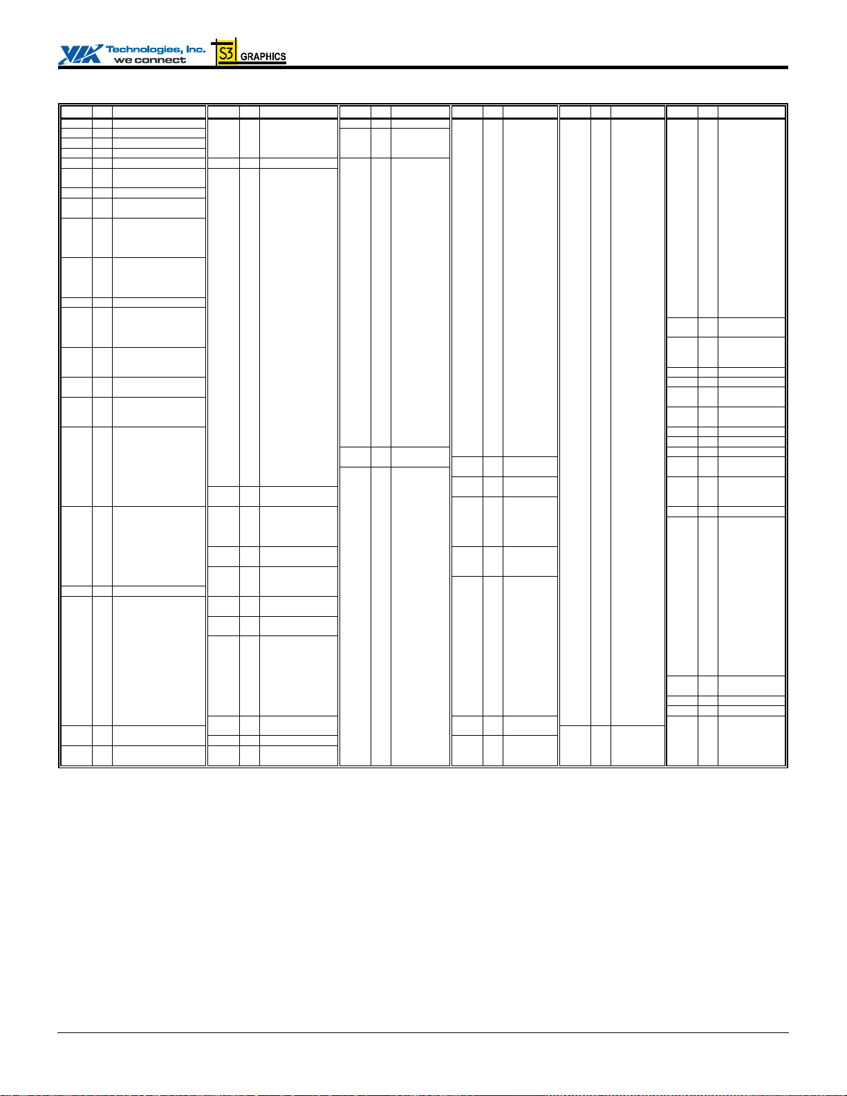
CN400 Data Sheet
Table 5. Pin List (Listed by Pin Name) - External AGP Interface Enabled (No Panel Interface)
Pin # Pin Name Pin # Pin Name Pin # Pin Name Pin # Pin Name Pin # Pin Name Pin # Pin Name
T01 AO AB AJ10 IO GC#BE0 AE05 O GST2 D08 IO HD30# K29 IO MD03 C04 – NC
A28 IO ADS# AH09 IO GC#BE1 AF09 IO GSTOP B04 IO HD31# H27 IO MD04 C06 – NC
T02 AO AG AK07 IO GC#BE2 AK08 IO GTRDY C05 IO HD32# H28 IO MD05 C07 – NC
AD02 I AGP8XDET# AH06 IO GC#BE3 AE03 I GWBF D06 IO HD33# J27 IO MD06 C11 – NC
AE21 O AGPBUSY# / NMI P06 I GCLK C19 IO HA03# B02 IO HD34# K30 IO MD07 C24 – NC
AE02 AI AGPCOMPN AE11 IO GD0 B21 IO HA04# F07 IO HD35# L30 IO MD08 C28 – NC
AE01 AI AGPCOMPP AG11 IO GD1 D19 IO HA05# E03 IO HD36# L27 IO MD09 D21 – NC
T03 AO AR AG12 IO GD2 D20 IO HA06# D01 IO HD37# P30 IO MD10 D27 – NC
AB26 O BA0 AF13 IO GD3 D22 IO HA07# C02 IO HD38# P28 IO MD11 E01 – NC
AB27 O BA1 AK12 IO GD4 C21 IO HA08# E02 IO HD39# L28 IO MD12 E06 – NC
U06 I BISTIN AF12 IO GD5 C20 IO HA09# H06 IO HD40# M30 IO MD13 E11 – NC
A21 IO BNR# AH12 IO GD6 C17 IO HA10# G04 IO HD41# N30 IO MD14 E12 – NC
B23 IO BPRI# AJ12 IO GD7 A20 IO HA11# F01 IO HD42# N29 IO MD15 E19 – NC
C27 O BREQ0# AF10 IO GD8 D18 IO HA12# C01 IO HD43# R30 IO MD16 F02 – NC
M26 O CKE0 AK10 IO GD9 C18 IO HA13# F04 IO HD44# R29 IO MD17 J02 – NC
K28 O CKE1 AH10 IO GD10 E22 IO HA14# F03 IO HD45# U30 IO MD18 J03 – NC
M27 O CKE2 AG09 IO GD11 B17 IO HA15# J01 IO HD46# U27 IO MD19 J05 – NC
K27 O CKE3 AK09 IO GD12 E18 IO HA16# F05 IO HD47# P27 IO MD20 L04 – NC
D16 O CPURST# AG10 IO GD13 F15 IO HA17# H05 IO HD48# R28 IO MD21 AG13 – NC
AH26 O CS0# AJ09 IO GD14 F14 IO HA18# G03 IO HD49# U28 IO MD22 AH13 – NC
AH25 O CS1# AE12 IO GD15 A16 IO HA19# K06 IO HD50# V30 IO MD23 AG21 I PWROK
AG25 O CS2# AH07 IO GD16 D15 IO HA20# G01 IO HD51# V29 IO MD24 AH21 I RESET#
AG23 O CS3# AG07 IO GD17 E16 IO HA21# J04 IO HD52# W30 IO MD25 C26 IO RS0#
B26 IO DBSY# AK06 IO GD18 C16 IO HA22# K01 IO HD53# Y28 IO MD26 C25 IO RS1#
A24 IO DEFER# AF07 IO GD19 A15 IO HA23# K03 IO HD54# AA30 IO MD27 B27 IO RS2#
F28 I DFTIN# AJ06 IO GD20 E15 IO HA24# H03 IO HD55# V28 IO MD28 V04 AI RSET
P02 I DISPCLKI AE07 IO GD21 F16 IO HA25# L02 IO HD56# W28 IO MD29 AG26 O SCAS#
P03 O DISPCLKO AE08 IO GD22 E14 IO HA26# H02 IO HD57# Y27 IO MD30 AB02 IO SPCLK1
AG18 O DNCMD AK05 IO GD23 C15 IO HA27# K04 IO HD58# AA29 IO MD31 W02 IO SPCLK2
AF16 O DNSTB+ AJ03 IO GD24 E17 IO HA28# H04 IO HD59# AA28 IO MD32 AB03 IO SPDAT1
AF17 O DNSTB– AG06 IO GD25 C14 IO HA29# L06 IO HD60# AA27 IO MD33 V03 IO SPDAT2
J30 O DQM0 AH05 IO GD26 B15 IO HA30# L03 IO HD61# AC27 IO MD34 AG27 O SRAS#
M28 O DQM1 AK03 IO GD27 B16 IO HA31# L01 IO HD62# AD27 IO MD35 AJ21 I SUSST#
T29 O DQM2 AH04 IO GD28 N05 I HCLK+ H01 IO HD63# AB30 IO MD36 AF25 O SWE#
Y30 O DQM3 AH03 IO GD29 N06 I HCLK– E25 IO HIT# AB29 IO MD37 N07 I TCLK
AC28 O DQM4 AK01 IO GD30 D13 IO HD00# B25 I HITM# AD29 IO MD38 F27 I TESTIN#
AG29 O DQM5 AK02 IO GD31 E13 IO HD01# E24 I HLOCK# AD28 IO MD39 AG19 I UPCMD
AK29 O DQM6 AF06 IO GDBIH / GPIPE# E09 IO HD02# F13 AI HRCOMP AE27 IO MD40 AH17 I UPSTB+
AK24 O DQM7 AG05 IO GDBIL F09 IO HD03# A25 IO HREQ0# AF28 IO MD41 AJ17 I UPSTB–
J29 IO DQS0# AK11 IO GADSTB0F B13 IO HD04# C22 IO HREQ1# AG30 IO MD42 AG16 IO VBE#
M29 IO DQS1# AH11 IO GADSTB0S A12 IO HD05# B24 IO HREQ2# AH29 IO MD43 AH16 IO VD00
T30 IO DQS2# AK04 IO GADSTB1F C13 IO HD06# D24 IO HREQ3# AE28 IO MD44 AG15 IO VD01
W29 IO DQS3# AJ04 IO GADSTB1S F08 IO HD07# C23 IO HREQ4# AF27 IO MD45 AH18 IO VD02
AC30 IO DQS4# AJ07 IO GDEVSEL C12 IO HD08# V01 O HSYNC AG28 IO MD46 AF18 IO VD03
AF30 IO DQS5# AE09 IO GFRAME D12 IO HD09# D25 IO HTRDY# AH30 IO MD47 AF15 IO VD04
AK28 IO DQS6# AD03 O GGNT B11 IO HD10# V05 O INTA# AH28 IO MD48 AH15 IO VD05
AJ24 IO DQS7# AH08 IO GIRDY C09 IO HD11# Y25 O MA00 AJ30 IO MD49 AH19 IO VD06
A27 IO DRDY# AE10 IO GPAR C10 IO HD12# AA26 O MA01 AJ27 IO MD50 AF19 IO VD07
W03 O DVP0D00 / TVD00 AA02 O GPO0 A08 IO HD13# W26 O MA02 AK26 IO MD51 AH14 IO VD08
W04 O DVP0D01 / TVD01 U07 O GPOUT D09 IO HD14# W27 O MA03 AJ28 IO MD52 AJ14 IO VD09
Y03 O DVP0D02 / TVD02 AE06 I GRBF A13 IO HD15# V26 O MA04 AK30 IO MD53 AK20 IO VD10
AA03 O DVP0D03 / TVD03 AD04 I GREQ A07 IO HD16# T27 O MA05 AH27 IO MD54 AH20 IO VD11
V06 O DVP0D04 / TVD04 AF03 I GSBA0# B12 IO HD17# V27 O MA06 AK27 IO MD55 AJ13 IO VD12
Y04 O DVP0D05 / TVD05 AF01 I GSBA1# D10 IO HD18# R27 O MA07 AK25 IO MD56 AK13 IO VD13
AA05 O DVP0D06 / TVD06 AF04 I GSBA2# B07 IO HD19# T28 O MA08 AH24 IO MD57 AG20 IO VD14
AA04 O DVP0D07 / TVD07 AG01 I GSBA3# C08 IO HD20# R26 O MA09 AK22 IO MD58 AK21 IO VD15
AB05 O DVP0D08 / TVD08 AG04 I GSBA4# D07 IO HD21# AB28 O MA10 AH22 IO MD59 AE14 AI VLCOMPP
AC03 O DVP0D09 / TVD09 AH01 I GSBA5# C03 IO HD22# N28 O MA11 AJ25 IO MD60 AF14 IO VPAR
AB04 O DVP0D10 / TVD10 AJ01 I GSBA6# E07 IO HD23# N27 O MA12 AG24 IO MD61 V02 O VSYNC
AD01 O DVP0D11 / TVD11 AH02 I GSBA7# B06 IO HD24# AH23 O MA13 AK23 IO MD62 P07 I XIN
Y05 O DVP0CK / TVCK AG03 I GSBSTBF A05 IO HD25# F29 I MCLKI AJ22 IO MD63
AC04 O DVP0DE / TVDE AG02 I GSBSTBS A06 IO HD26# F30 O MCLKO A22 – NC
AC01 I DVP0DET / TVCKIN AG08 IO GSERR D03 IO HD27# G30 IO MD00 B14 – NC
Y02 O DVP0HS / TVHS AD05 O GST0 A03 IO HD28# H30 IO MD01 B22 – NC
W05 O DVP0VS / TVVS AE04 O GST1 A04 IO HD29# J28 IO MD02 B28 – NC
Revision 1.18, January 26, 2005 -15- Pin Lists

CN400 Data Sheet
Table 6. Power, Ground and Voltage Reference Pin List
Outer Ring Pins (Intermixed with Signal Pins)
AGPVREF[0:1] (2 pins): AE13, AD6
GTLVREF (1 pin): G15
HAVREF[0:1] (2 pins): F18,20
HDVREF[0:3] (4 pins): G10,13, K7, J7
HCOMPVREF (1 pin): G14
MEMVREF[0:5] (6 pins): H26, L25, R25, W25, AC25, AE22
VLVREF (1 pin): AE15
VCCA33HCK1 (1 pin): M1
GNDAHCK1 (1 pin): M2
VCCA33HCK2 (1 pin): M4
GNDAHCK2 (1 pin): M5
VCCA33GCK (1 pin): M3
GNDAGCK (1 pin): M6
VCCA33MCK (1 pin): G28
GNDAMCK (1 pin): G27
VCCA15PLL1 (1 pin): N3
GNDAPLL1 (1 pin): N4
VCCA15PLL2 (1 pin): P4
GNDAPLL2 (1 pin): P5
VCCA15PLL3 (1 pin): N1
GNDAPLL3 (1 pin): N2
VCCA33DAC[1:2] (2 pins): R4, U4
GNDADAC[1:3] (3 pins): R5, T4, U5
VSUS15 (1 pin): AF21
GND (63 pins): A11,14,17,23,26,29, B3,5,8,20, D2,5,11,14,17,23,26,29, E8,20,30, F17, G2,5,8,16,29, H29, J26, K2,5, L26,29, P26,29, U26,29, Y26,29,
AC2,5,26,29, AF2,5,8,11,20,23,26,29, AG14,17, AJ2,5,8,11,20,23,26,29, AK14,17
Center Pins
VCC15 (51 pins): J9-22, K9,22, L9,22, M9,22, N9,22, P9,22, R9,22, T9,22, U9,22, V9,22, W9,22, Y9,22, AA9,22, AB9-21
VCC25MEM (20 pins): K18-21, L21, M21, N21, P21, R21, T21, U21, V21, W21, Y21, AA16-21
VCC15AGP (7 pins): V10, W10, Y10, AA10-13
VCC15VL (2 pins): AA14-15
VCC33GFX (3 pins): R10, T10, U10
VTT (12 pins): K10-17, L10, M10, N10, P10
GND (101 pins): L11-20, M11-20, N11-20, P11-20, R11-20, T11-20, U11-20, V11-20, W11-20, Y11-20
Revision 1.18, January 26, 2005 -16- Pin Lists
CN400 Data Sheet
Pin Descriptions
CPU Interface Pin Descriptions
CPU Interface
Signal Name Pin # I/O Signal Description
HA[31:3]#
HD[63:0]#
ADS#
BNR#
BPRI#
DBSY#
DEFER#
DRDY#
HIT#
HITM#
HLOCK#
HREQ[4:0]#
HTRDY#
RS[2:0]#
CPURST#
BREQ0#
Note: Clocking of the CPU interface is performed with HCLK+ and HCLK–.
Note: Internal pullup resistors are provided on all GTL interface pins. If the CPU does not have internal pullups, the North
Bridge internal pullups may be enabled to allow the interface to meet GTL bus interface specifications (see strap
descriptions).
Note: I/O pads for the above pins are powered by VTT. Input voltage levels are referenced to HAVREF, HDVREF and
GTLREF.
(see pin list) IO Host Address Bus. HA[31:3] connect to the address bus of the host CPU. During
CPU cycles HA[31:3] are inputs. These signals are driven by the North Bridge during
cache snooping operations.
(see pin list) IO Host CPU Data. These signals are connected to the CPU data bus.
A28 IO Address Strobe. The CPU asserts ADS# in T1 of the CPU bus cycle.
A21 IO Block Next Request. Used to block the current request bus owner from issuing new
requests. This signal is used to dynamically control the processor bus pipeline depth.
B23 IO Priority Agent Bus Request. The owner of this signal will always be the next bus
owner. This signal has priority over symmetric bus requests and causes the current
symmetric owner to stop issuing new transactions unless the HLOCK# signal is
asserted. The North Bridge drives this signal to gain control of the processor bus.
B26 IO Data Bus Busy. Used by the data bus owner to hold the data bus for transfers requiring
more than one cycle.
A24 IO Defer. A dynamic deferring policy is used to optimize system performance. The
DEFER# signal is also used to indicate a processor retry response.
A27 IO Data Ready. Asserted for each cycle that data is transferred.
E25 IO Hit. Indicates that a caching agent holds an unmodified version of the requested line.
Also driven in conjunction with HITM# by the target to extend the snoop window.
B25 I Hit Modified. Asserted by the CPU to indicate that the address presented with the last
assertion of EADS# is modified in the L1 cache and needs to be written back.
E24 I Host Lock. All CPU cycles sampled with the assertion of HLOCK# and ADS# until
the negation of HLOCK# must be atomic.
C23, D24, B24,
C22, A25
D25 IO Host Target Ready. Indicates that the target of the processor transaction is able to
B27, C25, C26 IO Response Signals. Indicates the type of response per the table below:
D16 O CPU Reset. Reset output to CPU. External pullup and filter capacitor to ground
C27 O Bus Request 0. Connect to CPU bus request 0.
IO Request Command. Asserted during both clocks of the request phase. In the first
clock, the signals define the transaction type to a level of detail that is sufficient to
begin a snoop request. In the second clock, the signals carry additional information to
define the complete transaction type.
enter the data transfer phase.
RS[2:0]# Response type
000 Idle State
001 Retry Response
010 Defer Response
011 Reserved
100 Hard Failure
101 Normal Without Data
110 Implicit Writeback
111 Normal With Data
should be provided per CPU manufacturer’s recommendations.
Revision 1.18, January 26, 2005 -17- Pin Descriptions

CN400 Data Sheet
The pinouts were defined assuming the ATX PCB layout model shown below (and general pin layout shown) as a guide for PCB
component placement. Other PCB layouts (AT, LPX and NLX) were also considered and can typically follow the same general
component placement.
PCI Slots
VT8237R
V-Link
South
Bridge
AGP
Slot
VIA C3
CPU
1 … 36
CPU
GFX
AGP
VL
CN
400
SDRAM
A
…
AT
DDR
SDRAM
Modules
IDE Connectors
Power
Supply
DDR SDRAM Memory Controller Pin Descriptions
DDR DRAM Interface
Signal Name Pin # I/O Signal Description
MA[13:0]
BA[1:0]
SRAS#, SCAS#, SWE# AG27, AG26, AF25 O
MD[63:0]
DQM[7:0]
AK24, AK29, AG29, AC28,
DQS[7:0]# AJ24, AK28, AF30, AC30,
CS[3:0]#
CKE[3:0]
Note: I/O pads for all pins on this page are powered by VCC25MEM. MD / DQS input voltage levels are referenced to
MEMVREF.
(see pin lists) O Memory Address. Output drive strength may be set by
Device 0 Function 3 RxE8.
AB27, AB26 O Bank Address. Output drive strength may be set by
Device 0 Function 3 RxE8.
Row Address, Column Address and Write Enable
Command Indicators. Output drive strength may be set
by Device 0 Function 3 Rx E8.
(see pin lists) IO Memory Data. These signals are connected to the
DRAM data bus. Output drive strength may be set by
Device 0 Function 3 RxE2.
O Data Mask. Data mask of each byte lane. Output drive
Y30, T29, M28, J30
strength may be set by Device 0 Function 3 RxE2.
IO DDR Data Strobe. Data strobe of each byte lane. Output
W29, T30, M29, J29
drive strength may be set by Device 0 Function 3 RxE0.
AG23, AG25, AH25, AH26 O Chip Select. Chip select of each bank. Output drive
strength may be set by Device 0 Function 3 RxE4.
K27, M27, K28, M26 O Clock Enables. Clock enables for each DRAM bank for
powering down the SDRAM or clock control for reducing
power usage and for reducing heat / temperature in highspeed memory systems.
Revision 1.18, January 26, 2005 -18- Pin Descriptions
CN400 Data Sheet
Accelerated Graphics Port Pin Descriptions
AGP 8x / 4x Bus Interface
Signal Name Pin # I/O Signal Description
(see
GD[31:0]
pin list)
GC#BE[3:0]
(GCBE#[3:0]
for 4x mode)
GPAR
GDBIH / GPIPE#
GDBIL
GADSTB0F
AH6,
AK7,
AH9,
AJ10
AE10 IO AGP Parity. A single parity bit is provided over GD[31:0] and GBE[3:0].
AF6
AG5
AK11
(GADSTB0 for 4x),
GADSTB0S
AH11
(GADSTB0# for 4x)
GADSTB1F
AK4
(GADSTB1 for 4x),
GADSTB1S
(GADSTB1# for 4x)
GFRAME
AE9 IO Frame. Assertion indicates the address phase of a PCI transfer. Negation indicates that
(GFRAME# for 4x)
GDEVSEL
(GDEVSEL# for 4x)
GIRDY
AH8 IO Initiator Ready. (Interpreted as active low for PCI/AGP4x and high for AGP 8x). For
(GIRDY# for 4x)
GTRDY
AK8 IO Target Ready. (Interpreted as active low for PCI/AGP4x and high for AGP 8x). For
(GTRDY# for 4x)
Note: I/O pads for all pins on this page are powered by VCC15AGP. Input voltage levels are referenced to AGPVREF.
Note: The AGP interface pins can be optionally configured as additional interfaces for connecting to external display devices. For simplification of the AGP pin
description tables above and on the next page, that multiplexing is not shown here (see “Additional I2C Interfaces” and “Digital Display” pin description tables
later in this document for more information).
IO Address / Data Bus. Address is driven with GADSTB assertion for AGP-style transfers
and with GFRAME# assertion for PCI-style transfers.
IO Command / Byte Enable. (Interpreted as C/BE# for AGP 2x/4x and C#/BE for 8x). For
AGP cycles these pins provide command information (different commands than for PCI)
driven by the master (graphics controller) when requests are being enqueued using GPIPE#
(2x/4x only as GPIPE# isn’t used in 8x mode). These pins provide valid byte information
during AGP write transactions and are driven by the master. The target (this chip) drives
these lines to “0000” during the return of AGP read data. For PCI cycles, commands are
driven with GFRAME# assertion. Byte enables corresponding to supplied or requested
data are driven on following clocks.
IO Dynamic Bus Inversion High / Low. AGP 8x transfer mode only. Driven by the source
to indicate whether the corresponding data bit group (GDBIH for GD[31:16] and GDBIL
for GD[15:0]) needs to be inverted on the receiving end (1 on GDBIx indicates that the
corresponding data bit group should be inverted). Used to limit the number of
simultaneously switching outputs to 8 for each 16-pin group.
Pipelined Request. Not used by AGP 8x. Asserted by the master (external graphics
controller) to indicate that a full-width request is to be enqueued by the target (North
Bridge). The master enqueues one request each rising edge of GCLK while GPIPE# is
asserted. When GPIPE# is deasserted no new requests are enqueued across the AD bus.
Note: See RxAE[1] for GPIPE# / GDBIH pin function selection.
IO Bus Strobe 0. Source synchronous strobes for GD[15:0] (the agent that is providing the
data drives these signals). GADSTB0 and GADSTB0# provide timing for 4x mode. For
8x transfer mode, GADSTB0 is interpreted as GADSTB0F (“First” strobe) and
GADSTB0# as GADSTB0S (“Second” strobe).
IO Bus Strobe 1. Source synchronous strobes for GD[31:16] (i.e., the agent that is providing
AJ4
the data drives these signals). GADSTB1 and GADSTB1# provide timing for 4x transfer
mode. For 8x transfer mode, GADSTB1 is interpreted as GADSTB1F (“First” strobe) and
GADSTB1# as GADSTB1S (“Second” strobe).
one more data transfer is desired by the cycle initiator. Interpreted as active high for 8x.
AJ7 IO Device Select (PCI transactions only). This signal is driven by the North Bridge when a
PCI initiator is attempting to access main memory. It is an input when the chip is acting as
PCI initiator. Not used for AGP cycles. Interpreted as active high for AGP 8x.
AGP write cycles, the assertion of this pin indicates that the master is ready to provide all
write data for the current transaction. Once this pin is asserted, the master is not allowed to
insert wait states. For AGP read cycles, the assertion of this pin indicates that the master is
ready to transfer a subsequent block of read data. The master is never allowed to insert a
wait state during the initial block of a read transaction. However, it may insert wait states
after each block transfers. For PCI cycles, asserted when initiator is ready for data transfer.
AGP cycles, indicates that the target is ready to provide read data for the entire transaction
(when the transaction can complete within four clocks) or is ready to transfer a (initial or
subsequent) block of data when the transfer requires more than four clocks to complete.
The target is allowed to insert wait states after each block transfer for both read and write
transactions. For PCI cycles, asserted when the target is ready for data transfer.
Revision 1.18, January 26, 2005 -19- Pin Descriptions
CN400 Data Sheet
AGP 8x / 4x Bus Interface (continued)
Signal Name Pin # I/O Signal Description
AGP8XDET#
GRBF
(GRBF# for 4x)
GWBF
(GWBF# for 4x)
GSBA[7:0]#
(GSBA[7:0] for 4x)
GSBSTBF
(GSBSTB for 4x),
GSBSTBS
(GSBSTB# for 4x)
GST[2:0]
GREQ (GREQ# for 4x) AD4 I Request. Master (graphics controller) request for use of the AGP bus.
GGNT (GGNT# for 4x) AD3 O Grant. Permission is given to the master (graphics controller) to use the AGP
GSERR (GSERR# for 4x) AG8 IO
GSTOP (GSTOP# for 4x) AF9 IO Stop. Asserted by the target to request the master to stop the current
Note: I/O pads for all pins on this page are powered by VCC15AGP. Input voltage levels are referenced to AGPVREF.
Note: The AGP interface pins can be optionally configured as additional interfaces for connecting to external display devices. For simplification of the AGP pin
description tables above and on the next page, that multiplexing is not shown here (see “Additional I2C Interfaces” and “Digital Display” pin description
tables later in this document for more information).
Note: Separate system interrupts are not provided for AGP. The AGP connector provides interrupts via PCI bus INTA-B#.
Note: A separate reset is not required for the AGP bus (RESET# resets both PCI and AGP buses)
Note: Two mechanisms are provided by the AGP bus to enqueue master requests: GPIPE# (to send addresses multiplexed on the AD lines) and the SBA port (to
send addresses unmultiplexed). AGP masters implement one or the other or select one at initialization time (they are not allowed to change during
runtime). Only one of the two will be used; the signals associated with the other will not be used. GRBF# has an internal pullup to maintain it in the de-
asserted state in case it is not implemented on the master device. AGP 8x mode allows only SBA (GPIPE# isn’t used in 8x mode).
Note: AGP 8x signal levels are 0V and 0.8V. AGP 8x mode maintains most signals at a low level when inactive resulting in no current flow.
AD2 I AGP 8x Transfer Mode Detect. Low indicates that the external graphics card
can support 8x transfer mode
AE6 I Read Buffer Full. Indicates if the master (graphics controller) is ready to
accept previously requested low priority read data. When GRBF# is asserted,
the North Bridge will not return low priority read data to the graphics
controller.
AE3 I
AH2, AJ1,
AH1, AG4,
AG1, AF4,
Write Buffer Full.
I Side Band Address. Provides an additional bus to pass address and command
information from the master (graphics controller) to the target (North Bridge).
These pins are ignored until enabled.
AF1, AF3
AG3
AG2
I Side Band Strobe. Driven by the master to provide timing for GSBA[7:0].
GSBSTB and GSBSTB# are used together for AGP 4x. For 8x mode, the
strobe mechanism works differently with GSBSTB interpreted as GSBSTBF
(“First” strobe) and GSBSTB# as GSBSTBS (“Second” strobe).
AE5, AE4,
AD5
O Status (AGP only). Provides information from the arbiter to a master to
indicate what it may do. Only valid while GGNT# is asserted.
000 Indicates that previously requested low priority read or flush data is
being returned to the master (graphics controller).
001 Indicates that previously requested high priority read data is being
returned to the master.
010 Indicates that the master is to provide low priority write data for a
previously enqueued write command.
011 Indicates that the master is to provide high priority write data for a
previously enqueued write command.
100 Reserved. (arbiter must not issue, may be defined in the future).
101 Reserved. (arbiter must not issue, may be defined in the future).
110 Reserved. (arbiter must not issue, may be defined in the future).
111 Indicates that the master (graphics controller) has been given
permission to start a bus transaction. The master may enqueue
AGP requests by asserting GPIPE# or start a PCI transaction by
asserting GFRAME#. GST[2:0] are always outputs from the target
(North Bridge logic) and inputs to the master (graphics controller).
bus.
System Error.
transaction. Interpreted as active high for AGP 8x.
Revision 1.18, January 26, 2005 -20- Pin Descriptions
CN400 Data Sheet
Ultra V-Link Pin Descriptions
Ultra V-Link Interface
Signal Name Pin # I/O Signal Description
V-Link Data Bus. During system initialization, VD[7:0] are used to transmit strap
VD15,
VD14,
VD13,
VD12,
VD11,
VD10,
VD9,
VD8,
VD7,
VD6,
VD5,
VD4,
VD3,
VD2,
VD1,
VD0
VPAR
VBE#
UPCMD
UPSTB+
UPSTB–
DNCMD
DNSTB+
DNSTB–
Note: I/O pads for the pins in the above table are powered by VCC15VL. Input voltage levels are referenced to VLVREF.
AK21,
AG20,
AK13,
AJ13,
AH20,
AK20,
AJ14,
AH14,
AF19,
AH19,
AH15,
AF15,
AF18,
AH18,
AG15,
AH16
AF14 IO
AG16 IO
AG19 I
AH17 I
AJ17 I
AG18 O
AF16 O
AF17 O
IO
information from the South Bridge (the straps are not on the VD pins but are on the
IO
indicated pins of the South Bridge chip). Check the strap pin table for details.
IO
IO
IO
IO
IO
IO
IO
IO
IO
IO
IO
IO
IO
IO
V-Link Parity.
V-Link Byte Enable.
V-Link Command from Client (South Bridge) to Host (North Bridge).
V-Link Strobe from Client to Host.
V-Link Complement Strobe from Client to Host.
V-Link Command from Host (North Bridge) to Client (South Bridge).
V-Link Strobe from Host to Client.
V-Link Complement Strobe from Host to Client.
Revision 1.18, January 26, 2005 -21- Pin Descriptions
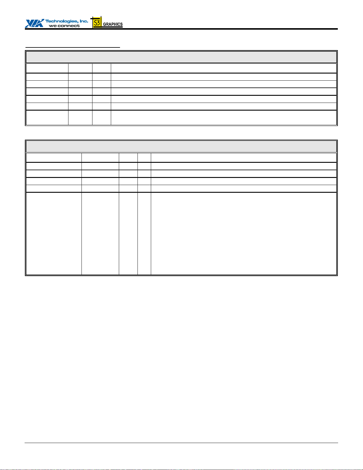
CN400 Data Sheet
CRT and Serial Bus Pin Descriptions
CRT Interface
Signal Name Pin # I/O Signal Description
AR
AG
AB
HSYNC
VSYNC
RSET
I/O pads for the pins in the above table are powered by VCC33GFX (i.e., 3.3V I/O).
T3 AO Analog Red. Analog red output to the CRT monitor.
T2 AO Analog Green. Analog green output to the CRT monitor.
T1 AO Analog Blue. Analog blue output to the CRT monitor.
V1 O Horizontal Sync. Output to CRT.
V2 O Vertical Sync. Output to CRT.
V4 AI
Reference Resistor. Tie to GNDDAC through an external 82Ω 1% resistor to control the
RAMDAC full-scale current value.
SMB / I2C Interface
Signal Name AGP Name Pin # I/O Signal Description
SBPLCLK
SBPLDAT
SBDDCCLK
SBDDCDAT
SPCLK2
SPCLK1 / CAPD12
SPDAT2,
SPDAT1 / CAPD13
I/O pads for SPCLK[2:1] / SPDAT[2:1] above are powered by VCC33GFX (i.e., 3.3V I/O).
All other pins in the above table are powered by VCC15AGP (i.e., 1.5V I/O).
GIRDY AH8 IO
GC#BE1 AH9 IO
GREQ AD4 IO
GGNT AD3 IO
n/a
n/a
n/a
n/a
W2,
AB2
V3,
AB3
IO Serial Port (SMB/I2C) Clock and Data. The SPCLKn pins are the
I2C Serial Bus Clock for Panel (Muxed on AGP Bus Pins).
I2C Serial Bus Data for Panel (Muxed on AGP Bus Pins).
I2C Serial Bus Clock for CRT DDC (Muxed on AGP Bus Pins).
I2C Serial Bus Data for CRT DDC (Muxed on AGP Bus Pins).
clocks for serial data transfer. The SPDATn pins are the data signals used
for serial data transfer. SPxxx1 is typically used for DVI monitor
communications and SPxxx2 is typically used for DDC for CRT monitor
communications. These pins are programmed via “Sequencer” graphics
registers (port 3C5) in the “Extended” VGA register space (see the
UniChrome-II Graphics Registers document for additional details). The
SPxxx1 registers are programmed via 3C5.31 (“IIC Serial Port Control 1”)
and the SPxxx2 registers are programmed via 3C5.26 (“IIC Serial Port
Control 0”). In both registers, the clock out state is programmed via bit-5
and the data out state via bit-4, clock in status may be read in bit-3 and data
in status in bit-2, and the port may be enabled via bit-0.
Revision 1.18, January 26, 2005 -22- Pin Descriptions
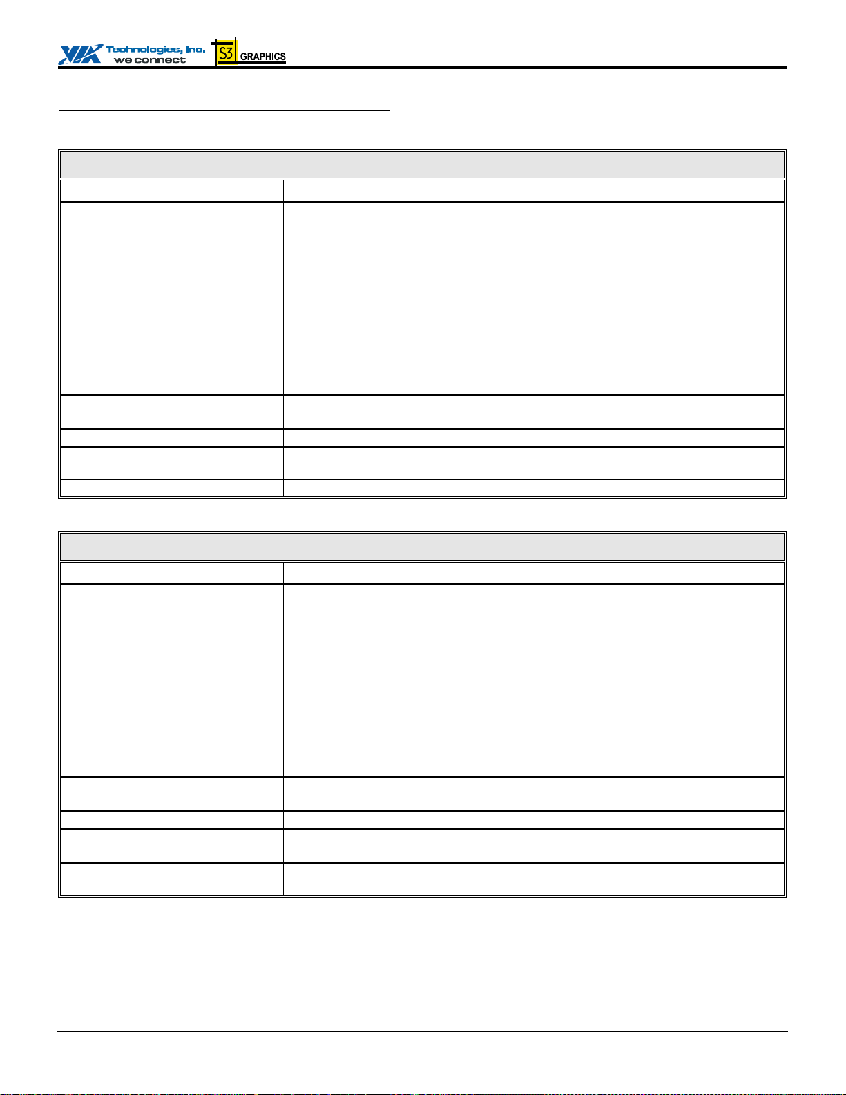
CN400 Data Sheet
Dedicated Digital Video Port 0 (DVP0) Pin Descriptions
The DVP0 dedicated Digital Video Port can be configured as either a TV Encoder interface port or a Video Capture input port,
selectable via strap pins DVP0D[6:5] (see the TV Encoder Interface and Video Capture Interface pin descriptions for details).
Dedicated Digital Video Port 0 (DVP0)
Signal Name Pin # I/O Signal Description
DVP0D11 / TVD11 / CAPD11,
DVP0D10 / TVD10 / CAPD10 / strap,
DVP0D9 / TVD9 / CAPD9 / strap,
DVP0D8 / TVD8 / CAPD8 / strap,
DVP0D7 / TVD7 / CAPD7 / strap,
DVP0D6 / TVD6 / CAPD6 / strap,
DVP0D5 / TVD5 / CAPD5 / strap,
DVP0D4 / TVD4 / CAPD4 / strap,
DVP0D3 / TVD3 / CAPD3 / strap,
DVP0D2 / TVD2 / CAPD2 / strap,
DVP0D1 / TVD1 / CAPD1 / strap,
DVP0D0 / TVD0 / CAPD0 / strap
DVP0HS / TVHS / CAPHS Y2 O Digital Video Port 0 Horizontal Sync. Internally pulled down.
DVP0VS / TVVS / CAPVS W5 O Digital Video Port 0 Vertical Sync. Internally pulled down.
DVP0DE / TVDE AC4 O Digital Video Port 0 Data Enable. Internally pulled down.
DVP0DET / TVCLKIN / CAPBCLK AC1 I Digital Video Port 0 Display Detect. If VGA register 3C5.12[5]=0,
DVP0CLK / TVCLK / CAPACLK Y5 O Digital Video Port 0 Clock. Internally pulled down.
The terminology “3C5.nn” above refers to the VGA “Sequencer” registers at I/O port 3C5 index “nn”
AD1,
AB4,
AC3,
AB5,
AA4,
AA5,
Y4,
V6,
AA3,
Y3,
W4,
W3
O Digital Video Port 0 Data. Default output drive is 8 mA. 16 mA may be
selected via SR3D[6]=1.
NOTE: DVP0D[6:0] are also used for power-up reset straps for the
embedded graphics controller. Check the Strap Pin table for details.
3C5.1A[5] will read 1 if display is connected. Tie to GND if not used.
Dedicated Digital Video Port 0 (DVP0) - TV Encoder Interface
Signal Name Pin # I/O Signal Description
TVD11 / DVP0D11 / CAPD11,
TVD10 / DVP0D10 / CAPD10 / strap,
TVD9 / DVP0D9 / CAPD9 / strap,
TVD8 / DVP0D8 / CAPD8 / strap,
TVD7 / DVP0D7 / CAPD7 / strap,
TVD6 / DVP0D6 / CAPD6 / strap,
TVD5 / DVP0D5 / CAPD5 / strap,
TVD4 / DVP0D4 / CAPD4 / strap,
TVD3 / DVP0D3 / CAPD3 / strap,
TVD2 / DVP0D2 / CAPD2 / strap,
TVD1 / DVP0D1 / CAPD1 / strap,
TVD0 / DVP0D0 / CAPD0 / strap
TVHS / DVP0HS / CAPHS Y2 O TV Encoder 0 Horizontal Sync. Internally pulled down.
TVVS / DVP0VS / CAPVS W5 O TV Encoder 0 Vertical Sync. Internally pulled down.
TVDE / DVP0DE AC4 O TV Encoder 0 Display Enable. Internally pulled down.
TVCLKIN / DVP0DET / CAPBCLK AC1 I TV Encoder 0 Clock In. Input from TV encoder. Internally pulled
TVCLK / DVP0CLK / CAPACLK Y5 O TV Encoder 0 Clock Out. Output to TV encoder. Internally pulled
The above pins may be connected to an external TV Encoder chip such as a VIA VT1625 for driving a TV set. I/O pads for the
pins on this page are powered by VCC33GFX (3.3V I/O).
AD1,
AB4,
AC3,
AB5,
AA4,
AA5,
Y4,
V6,
AA3,
Y3,
W4,
W3
O
TV Encoder 0 Data.
To configure DVP0 as a TV Out interface port, pins DVP0D[6:5] must be
strapped high.
Note: One TV Encoder interface is supported through either DVP0 or
GDVP1.
down.
down.
Revision 1.18, January 26, 2005 -23- Pin Descriptions
 Loading...