

Page 1

Data Sheet
CLE266
Version CD/CE
North Bridge
Revision 2.06
December 1, 2004
VIA TECHNOLOGIES, INC.
Page 2

Copyright Notice:
Copyright © 2002-2004 VIA Technologies Incorporated. All Rights Reserved. No part of this document may be reproduced, transmitted,
transcribed, stored in a retrieval system, or translated into any language, in any form or by any means, electronic, mechanical, magnetic, optical,
chemical, manual or otherwise without the prior written permission of VIA Technologies Incorporated. The material in this document is for
information only and is subject to change without notice. VIA Technologies Incorporated reserves the right to make changes in the product design
without reservation and without notice to its users.
Copyright © 2002-2004 S3 Graphics Incorporated. All rights reserved. If you have received this document from S3 Graphics Incorporated in
electronic form, you are permitted to make the following copies for business use related to products of S3 Graphics Incorporated: one copy onto your
computer for the purpose of on-line viewing, and one printed copy. With respect to all documents, whether received in hard copy or electronic form,
other use, copying or storage, in whole or in part, by any means electronic, mechanical, photocopying or otherwise, is not permitted without the prior
written consent of S3 Graphics Incorporated. The material in this document is for information only and is subject to change without notice. S3
Graphics Incorporated reserves the right to make changes in the product design without reservation and without notice to its users.
Trademark Notices:
VT8233A and CLE266 may only be used to identify products of VIA Technologies
C3™ is a registered trademark of VIA Technologies.
Windows XP™, Windows 2000™, Windows ME™, Windows 98™ and Plug and Play™ are registered trademarks of Microsoft Corporation.
PCI™ is a registered trademark of the PCI Special Interest Group.
PS/2™ is a registered trademark of International Business Machines Corporation.
VESA™ is a trademark of the Video Electronics Standards Association.
All trademarks are the properties of their respective owners.
Disclaimer Notice:
No license is granted, implied or otherwise, under any patent or patent rights of VIA Technologies or S3 Graphics. VIA Technologies and S3
Graphics make no warranties, implied or otherwise, in regard to this document and to the products described in this document. The information
provided by this document is believed to be accurate and reliable as of the publication date of this document. However, VIA Technologies and S3
Graphics assume no responsibility for any errors in this document. Furthermore, VIA Technologies and S3 Graphics assume no responsibility for
the use or misuse of the information in this document and for any patent infringements that may arise from the use of this document. The
information and product specifications within this document are subject to change at any time, without notice and without obligation to notify any
person of such change.
Offices:
VIA Technologies Incorporated
Taiwan Office:
th
Floor, No. 533
8
Chung-Cheng Road, Hsin-Tien
Taipei, Taiwan ROC
Tel : (886-2) 2218-5452
Fax : (886-2) 2218-5453
Home page :
http://www.via.com.tw
VIA Technologies Incorporated
USA Office :
940 Mission Court
Fremont, CA 94539
USA
Tel : (510) 683-3300
Fax : (510) 683-3301 or (510) 687-4654
Home Page :
http://www.viatech.com
S3 Graphics Incorporated
USA Office:
1045 Mission Court
Fremont, CA 94539
USA
Tel : (510) 687-4900
Fax : (510) 687-4901
Home Page:
http://www.s3graphics.com
Page 3
CLE266 Version CD / CE Desktop North Bridge Data Sheet
REVISION HISTORY
Document Release Date Revision Initials
1.0 1/14/03 Initial public release, same as internal revision 0.92 with confidential watermark removed DH
1.01 4/8/03 Updated Table 1 in Overview to indicate correct CRT screen resolutions supported
Updated mechanical specs to fix incorrect JEDEC-spec reference
1.1 4/25/03 Changed chipset name to north bridge chip name and removed VT#
Changed incorrect figure captions to table captions
1.2 5/29/03 Added “Version CD” to cover page
Fixed supported screen and LCD resolutions (1400x1050 max)
2.0 5/29/03 Changed “Version CD” to “Version CD / CE” DH
2.01 7/1/03 Removed 8MB Frame Buffer support
Fixed internal AGP speed & resolutions supported in graphics feature bullets & overview
Removed CPU/DRAM 133/100 freq support; added “Version CD/CE” to page header
2.02 7/17/03 Added 8MB Frame Buffer support information in product features, Table 1 (supported
CRT screen resolutions) and register setting of Device 0 RxE1[6:4]
Fixed typo of VCC25 information in notes of the pin list
2.03 3/22/04 Updated cover page, legal page and header
Updated the RSET resistor value in pin description table
Capitalized north bridge and south bridge
Modified the name of table 2 and table 3
Modified legend in mechanical specification
2.04 4/19/04 Added mechanical specifications for lead-free concern EY
2.05 8/11/04 Updated mechanical specification figure SV
2.06 12/1/04 Updated top marking in mechanical specificaiton VL
DH
DH
DH
DH
AL
SV
Revision 2.06, December 1, 2004 -i- Revision History
Page 4
CLE266 Version CD / CE Desktop North Bridge Data Sheet
TABLE OF CONTENTS
REVISION HISTORY .......................................................................................................................................................................I
TABLE OF CONTENTS.................................................................................................................................................................. II
LIST OF FIGURES .........................................................................................................................................................................IV
LIST OF TABLES ...........................................................................................................................................................................IV
PRODUCT FEATURES.................................................................................................................................................................... 1
CLE266 SYSTEM OVERVIEW ...................................................................................................................................................... 5
CLE266 VERSION CD / CE OVERVIEW....................................................................................................................................... 5
SYSTEM POWER MANAGEMENT ................................................................................................................................................... 6
HIGH-PERFORMANCE 3D ACCELERATOR.................................................................................................................................... 6
128-BIT 2D GRAPHICS ENGINE ..................................................................................................................................................... 6
DVD PLAYBACK AND VIDEO CONFERENCING ............................................................................................................................. 6
TV DISPLAY OUTPUT SUPPORT .................................................................................................................................................... 7
VIDEO CAPTURE INTERFACE ........................................................................................................................................................ 7
LCD, FLAT PANEL MONITOR AND TV OUTPUT DISPLAY SUPPORT........................................................................................... 7
HIGH SCREEN RESOLUTION CRT SUPPORT ................................................................................................................................7
PINOUTS............................................................................................................................................................................................ 8
PIN DESCRIPTIONS....................................................................................................................................................................... 11
REGISTERS..................................................................................................................................................................................... 19
REGISTER OVERVIEW ................................................................................................................................................................. 19
MISCELLANEOUS I/O................................................................................................................................................................... 30
PCI CONFIGURATION SPACE I/O ............................................................................................................................................... 30
DEVICE 0 REGISTER DESCRIPTIONS........................................................................................................................................... 31
Device 0 Host Bridge Header Registers .............................................................................................................................. 31
Device 0 Host Bridge Device-Specific Registers................................................................................................................. 33
V-Link Control...................................................................................................................................................................................... 33
Host CPU Control .................................................................................................................................................................................36
DRAM Control...................................................................................................................................................................................... 37
PCI Bus Control ....................................................................................................................................................................................43
GART / Graphics Aperture Control ......................................................................................................................................................45
AGP Control.......................................................................................................................................................................................... 46
V-Link Control...................................................................................................................................................................................... 48
Power Management............................................................................................................................................................................... 49
Frame Buffer and High Memory Control.............................................................................................................................................. 50
BIOS Scratch......................................................................................................................................................................................... 50
DEVICE 1 REGISTER DESCRIPTIONS........................................................................................................................................... 51
Device 1 PCI-to-PCI Bridge Header Registers .................................................................................................................. 51
Device 1 PCI-to-PCI Bridge Device-Specific Registers ..................................................................................................... 53
Internal AGP Bus Control ..................................................................................................................................................................... 53
Power Management............................................................................................................................................................................... 55
Revision 2.06, December 1, 2004 -ii- Table of Contents
Page 5
CLE266 Version CD / CE Desktop North Bridge Data Sheet
FUNCTIONAL DESCRIPTION.................................................................................................................................................... 56
INTEGRATED GRAPHICS CONTROLLER ...................................................................................................................................... 56
Internal Architecture ........................................................................................................................................................... 56
GRAPHICS MODES ....................................................................................................................................................................... 57
Desktop Modes - Single Display .......................................................................................................................................... 57
Desktop Modes - LCD VGA 640x480 Multiple Display .................................................................................................... 58
Desktop Modes - LCD SVGA 800x600 Multiple Display.................................................................................................. 59
Desktop Modes - LCD XGA 1024x768 Multiple Display.................................................................................................. 60
Desktop Modes - LCD SXGA 1280x1024 Multiple Display.............................................................................................. 61
Desktop Modes - LCD SXGA+ 1400x1050 Multiple Display............................................................................................ 62
Graphics Modes That Allow LCD Centering and Expansion .......................................................................................... 63
VGA Graphics Modes .......................................................................................................................................................... 64
Direct Draw Graphics Modes .............................................................................................................................................. 65
Graphics Modes for TV Display.......................................................................................................................................... 66
Additional Graphics Modes for IA Devices........................................................................................................................ 67
FLAT PANEL DISPLAY RGB MAPPING ....................................................................................................................................... 68
ELECTRICAL SPECIFICATIONS .............................................................................................................................................. 69
ABSOLUTE MAXIMUM RATINGS ................................................................................................................................................. 69
DC CHARACTERISTICS................................................................................................................................................................ 69
AC TIMING SPECIFICATIONS...................................................................................................................................................... 69
MECHANICAL SPECIFICATIONS............................................................................................................................................. 70
Revision 2.06, December 1, 2004 -iii- Table of Contents
Page 6

CLE266 Version CD / CE Desktop North Bridge Data Sheet
LIST OF FIGURES
FIGURE 1. SYSTEM BLOCK DIAGRAM.................................................................................................................................... 5
FIGURE 2. BALL DIAGRAM (TOP VIEW)................................................................................................................................. 8
FIGURE 3. GRAPHICS APERTURE ADDRESS TRANSLATION......................................................................................... 45
FIGURE 4. GRAPHICS CONTROLLER INTERNAL BLOCK DIAGRAM.......................................................................... 56
FIGURE 5. MECHANICAL SPECIFICATIONS – 548-PIN 27X27MM BALL GRID ARRAY PACKAGE WITH 1MM
BALL PITCH.............................................................................................................................................................. 70
FIGURE 6. LEAD-FREE MECHANICAL SPECIFICATIONS – 548-PIN 27X27MM BALL GRID ARRAY PACKAGE
WITH 1MM BALL PITCH ........................................................................................................................................ 71
LIST OF TABLES
TABLE 1. SUPPORTED CRT SCREEN RESOLUTIONS.......................................................................................................... 7
TABLE 2. PIN LIST (LISTED BY PIN NUMBER)...................................................................................................................... 9
TABLE 3. PIN LIST (LISTED BY PIN NAME) ......................................................................................................................... 10
TABLE 4. PIN DESCRIPTIONS .................................................................................................................................................. 11
TABLE 5. REGISTERS ................................................................................................................................................................. 19
TABLE 6. SYSTEM MEMORY MAP.......................................................................................................................................... 37
TABLE 7. MA MAP TYPE ENCODING..................................................................................................................................... 38
TABLE 8. MEMORY ADDRESS MAPPING TABLE ............................................................................................................... 38
TABLE 9. VGA / MDA MEMORY / IO REDIRECTION ......................................................................................................... 53
TABLE 10. DESKTOP GRAPHICS MODES – SINGLE DISPLAY ........................................................................................ 57
TABLE 11. DESKTOP GRAPHICS MODES – LCD VGA 640X480 MULTIPLE DISPLAY............................................... 58
TABLE 12. DESKTOP GRAPHICS MODES – LCD SVGA 800X600 MULTIPLE DISPLAY............................................. 59
TABLE 13. DESKTOP GRAPHICS MODES – LCD XGA 1024X768 MULTIPLE DISPLAY............................................. 60
TABLE 14. DESKTOP GRAPHICS MODES – LCD SXGA 1280X1024 MULTIPLE DISPLAY......................................... 61
TABLE 15. DESKTOP GRAPHICS MODES – LCD SXGA+ 1400X1050 MULTIPLE DISPLAY....................................... 62
TABLE 16. GRAPHICS MODES THAT ALLOW LCD CENTERING AND EXPANSION................................................. 63
TABLE 17. VGA GRAPHICS MODES........................................................................................................................................ 64
TABLE 18. DIRECT DRAW GRAPHICS MODES.................................................................................................................... 65
TABLE 19. GRAPHICS MODES FOR TV DISPLAY ............................................................................................................... 66
TABLE 20. ADDITIONAL GRAPHICS MODES FOR IA DEVICES ..................................................................................... 67
TABLE 21. FPD RGB MAPPING................................................................................................................................................. 68
TABLE 22. ABSOLUTE MAXIMUM RATINGS....................................................................................................................... 69
TABLE 23. DC CHARACTERISTICS......................................................................................................................................... 69
TABLE 24. AC TIMING MIN / MAX CONDITIONS................................................................................................................ 69
Revision 2.06, December 1, 2004 -iv- Table of Contents
Page 7

CLE266 Version CD / CE Desktop North Bridge Data Sheet
CLE266 VERSION CD / CE
NORTH BRIDGE
Single-Chip SMA North Bridge
with 133 / 100 / 66 MHz Front Side Bus for VIA C3 CPUs
with Integrated 2D / 3D AGP Graphics Core
plus Advanced DDR Memory Controller
supporting DDR266 / 200 DDR SDRAM
and PC133 / PC100 SDR SDRAM
for Desktop PC Systems
PRODUCT FEATURES
• Defines Integrated Solutions for Value PC Desktop Designs
– High performance SMA North Bridge: Integrated Apollo Pro266T and graphics accelerator in a single chip
– 64-bit advanced memory controller supporting DDR266 / 200 DDR SDRAM and PC133 / PC100 SDR SDRAM
– Combines with VIA VT8233A V-Link South Bridge for integrated audio, ATA-133 IDE and 4 USB ports
• High Performance CPU Interface
– Support for Socket-370 VIA C3 processors
– 133 / 100 / 66 MHz CPU Front Side Bus (FSB)
– Built-in Phase Lock Loop circuitry for optimal skew control within and between clocking regions
– Five outstanding transactions (Four In-Order Queue (IOQ) plus one output latch)
– Dynamic deferred transaction support
• High Bandwidth 266 MB / Sec 8-Bit V-Link Host Controller
– Supports 66 MHz V-Link Host interface with total bandwidth of 266 MB/Sec
– V-Link operates at 2x or 4x modes
– Full-duplex commands with separate strobe / command
– Request / Data split transaction
– Configurable outstanding transaction queue for Host to V-Link Client accesses
– Supports Defer / Defer-Reply transactions
– Transaction assurance for V-Link Host to Client access (eliminates V-Link Host-Client Retry cycles)
– Intelligent V-Link transaction protocol to minimize data wait-states / throttle transfer latency. All V-Link transactions
(both Host and Client) have a consistent view of transaction data depth and buffer size to avoid data overflow.
– Highly efficient V-Link arbitration with minimum overhead. All V-Link transactions have predictable cycle length
with known Command / Data duration.
Revision 2.06, December 1, 2004 -1- Product Features
Page 8

CLE266 Version CD / CE Desktop North Bridge Data Sheet
• Advanced High-Performance DDR / SDR DRAM Controller
– Supports DDR266 / 200 DDR SDRAM and PC133 / PC100 SDR SDRAM memory types
– DRAM interface synchronous with host CPU (133 / 100 MHz) for most flexible configuration
– DRAM interface may be faster or slower than CPU by 33 MHz
– Concurrent CPU, AGP and V-Link access
– Mixed 1M / 2M / 4M / 8M / 16M / 32M / 64MxN DRAMs
– Supports 4 banks up to 2 GB DRAMs (512Mb x8 / x16 DRAM technology)
– Flexible row and column addresses. 64-bit data width only
– LVTTL 3.3V DRAM interface with 2.5V SSTL-2 DRAM interface (DDR) and 5V-tolerant inputs (SDR)
– Programmable I/O drive capability for MA, command and MD signals
– Two-bank interleaving for 16Mbit SDRAM support
– Two-bank and four bank interleaving for 64Mbit SDRAM support
– Supports maximum 8-bank interleave (i.e., 8 pages open simultaneously); banks are allocated based on LRU
– Seamless DRAM command scheduling for maximum DRAM bus utilization (e.g., precharge other banks while
accessing the current bank)
– Four cache lines (16 quadwords) of CPU to DRAM write buffers
– Four cache lines of CPU to DRAM read prefetch buffers
– Read around write capability for non-stalled CPU read
– Speculative DRAM read before snoop result
– Burst read and write operation
– x-1/2-1/2-1/2-1-1/2-1/2-1/2 back-to-back accesses for DDR SDRAM (x-1-1-1-1-1-1-1 for SDR)
– Supports DDR SDRAM CL 2/2.5/3 and 1T per command
– Decoupled and burst DRAM refresh with staggered RAS timing (CAS before RAS or self refresh)
• Integrated Graphics / Video Accelerator
– Optimized Shared Memory Architecture (SMA)
– 8 / 16 / 32 / 64MB frame buffer using system memory
– Internal AGP 4x-equivalent performance
– Separate 128-bit data paths between North Bridge and graphics core for pixel data flow and texture / command
access
– Graphics engine clocks up to 133 MHz decoupled from memory clock
– Direct hardware inputs to force graphics accelerator into suspend / standby states
– High quality DVD video playback
– VIP 1.1 / VIP 2.0-compatible video capture inputs up to 165 MHz data rate
– Internal hardware VGA controller with true-color / high-color sprite for hardware cursor implementation
– 128-bit 2D graphics engine
– 128-bit 3D graphics engine
– Floating point triangle setup engine
– 3M triangles/second setup engine
– 133M pixels/second trilinear fill rate
• Extensive Display Support
– CRT display interface with 24-bit true-color RAMDAC up to 250 MHz pixel rate with gamma correction capability
– Direct TFT flat panel interface up to 24-bit data width supporting 18, 24 or 18+18 TFT panels or LVDS encoders
– 12-bit DVI 1.0-compatible interface for drive of flat panel monitor using external TMDS encoders
– Interface to external TV Encoder for NTSC or PAL TV display
– Flexible output configuration: CRT output plus 8-bit video capture port plus either 1) LCD Panel + DVI or TV-Out
or 2) DVI + TV-Out + 2
– Support for panel resolutions up to 1600x1200, CRT resolutions up to 1400x1050and DVI up to 1280x1024
– Automatic panel power sequencing and VESA DPMS CRT power-down
– Dual view capability where CRT and Flat Panel Monitor can have a different resolution and refresh rate
– Built-in reference voltage generator and monitor sense circuits
2
C Serial Bus and DDC Monitor Communications for CRT Plug-and-Play configuration
– I
nd
8-bit video capture port (or video capture port extension to 16-bit)
Revision 2.06, December 1, 2004 -2- Product Features
Page 9

CLE266 Version CD / CE Desktop North Bridge Data Sheet
• Video Support
– Up to three video windows for video conferencing applications
– High quality scaler (up or down) for both horizontal and vertical scaling (linear interpolation for horizontal and
vertical up-scaling and filtering for horizontal and vertical down-scaling)
– Color space conversion
– Color enhancement (contrast, hue, saturation, brightness and gamma correction)
– Color and chroma key support
– Hardware sub-picture blending
– Bob / weave de-interlacing mode and advanced de-interlacing to improve video quality
– Video capture inputs (one or two 8-bit ports or one 16-bit port) with built-in phase adjuster to fine tune the clock/data
signal timing
– PAL / NTSC TV output capability using external TV encoder
– Supports CCIR601standard
• MPEG-2/1 Video Decoder
– Motion compensation for full speed DVD playback
– Hardware accelerated Slice layer, IDCT and Motion compensation
• 2D Hardware Acceleration Features
– BitBLT (bit block transfer) functions including alpha blts
– Text function
– Bresenham line drawing / style line function
– ROP3, 256 operation
– Color expansion
– Source and destination color keys
– Transparency mode
– Window clipping
– 8, 15/16and 32 bpp mode acceleration
• 3D Hardware Acceleration Features
– Microsoft DirectX 7.0 and 8.0 compatible
– OpenGL driver available
– Floating-point setup engine
– Triangle rate up to 3-million triangles per second and Pixel rate up to 133-million pixels per second for 2 texture,
depth test and alpha blending
– Flat and Gouraud shading
– Hardware back-face culling
– 16-bit, 32-bit Z testand 24+8 Z+Stencil test support
– Z-Bias support
– Stipple Test, Line-Pattern test, Texture-Transparence test, Alpha test support
– Edge anti-aliasing support
– Two textures per pass
– Tremendous Texture Format: 16/32 bpp ARGB, 1/2/4/8 bpp Luminance, 1/2/4/8 bpp Intensity, 1/2/4/8 bpp Paletized
(ARGB), YUV 422/420 format
– Texture sizes up to 2048x2048
– High quality texture filter modes: Nearest, Linear, Bi-linear, Tri-linear, Anisotropic
– LOD-Bias support
– Vertex Fog and Fog Table
– Specular Lighting
– Alpha Blending
– High quality dithering
– ROP2 support
– Internal full 32-bit ARGB format for high rendering quality
– System balance to achieve high performance
Revision 2.06, December 1, 2004 -3- Product Features
Page 10

CLE266 Version CD / CE Desktop North Bridge Data Sheet
• Advanced System Power Management
– Power down of SDRAM (CKE)
– Independent clock stop controls for CPU / SDRAM and on-chip AGP bus
– Suspend power plane for preservation of memory data
– Suspend-to-DRAM and self-refresh power down
– Low-leakage I/O pads
– ACPI 1.0B and PCI Bus Power Management 1.1 compliant
• Full Software Support
– Drivers for major operating systems and APIs: [Windows 9x, Windows NT, Windows 2000, Windows XP,
Direct3D, DirectDraw and DirectShow, OpenGL ICD for Windows 9x, NT, 2000 and XP]
– North Bridge / Chipset and Video BIOS support (including all standard VESA CRT display modes)
• 2.5V Core and Mixed 3.3V / 5V Tolerant and GTL+ I/O
• 27 x 27mm Ball Grid Array Package with 548 Balls and 1mm Ball Pitch
Revision 2.06, December 1, 2004 -4- Product Features
Page 11
CLE266 Version CD / CE Desktop North Bridge Data Sheet
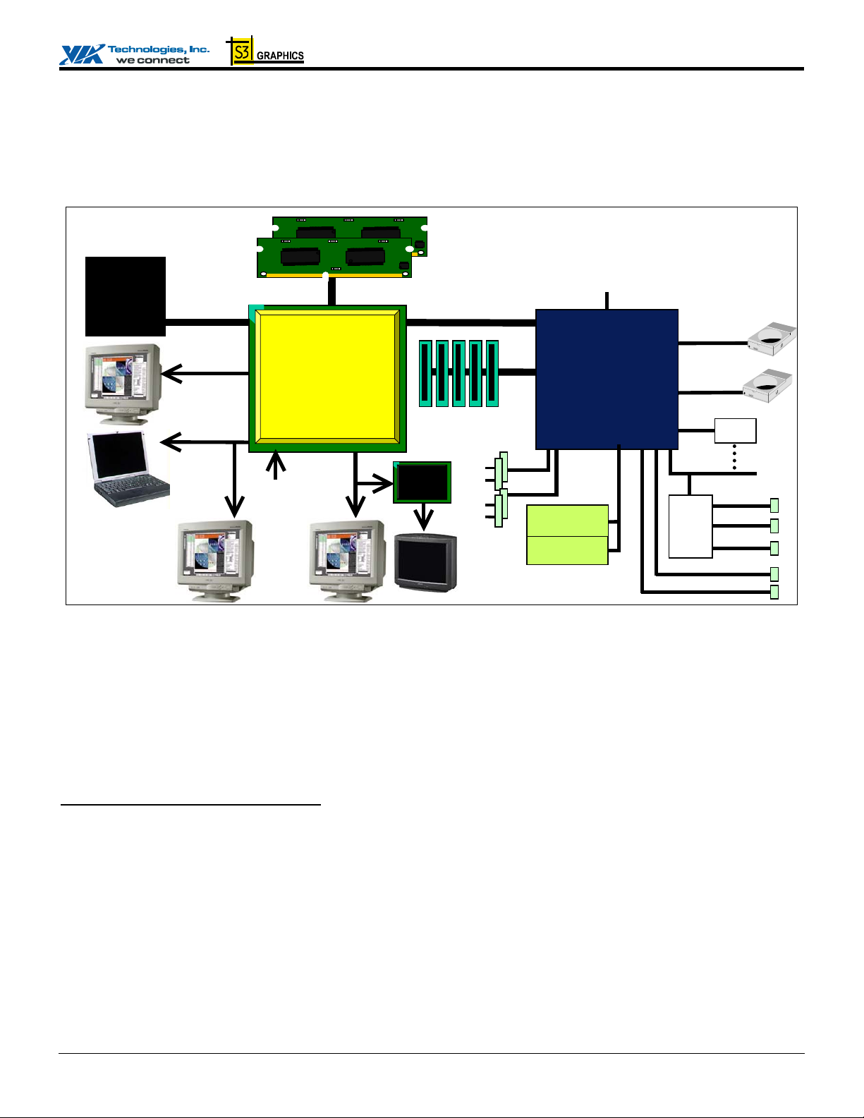
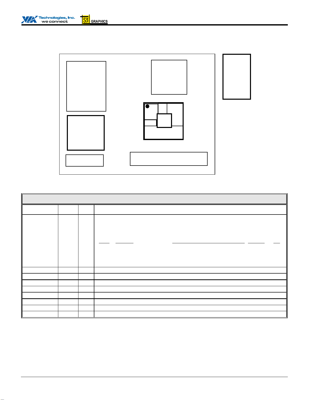
CLE266 SYSTEM OVERVIEW
CLE266 is a high performance, cost-effective and energy efficient SMA chipset North Bridge which may be used for the
implementation of desktop personal computer systems with 133 / 100 / 66 MHz CPU host bus (“Fron t Side Bus”) frequencies and
based on 64-bit Socket-370 VIA C3 processors.
System
VIA C3™
Socket-370
CPU
TFT Flat Panel
Flat
Panel
Monitor
133 or 100 MHz
Front Si de Bus
CRT
24-bit Direct
Panel Interface
or DVI plus 8-b it
Video Capture
Extension
64-bit 133 / 100 MHz DDR or SDR SDRAM
CLE266
SMA
North Bridge
548-pin HSBGA
12-bit DVI
or TV Out
8-Bit
Video
Capture
Port
Flat
Panel
Monitor
Figure 1. System Block Diagram
66 MHz QDR, 8-bit V-Link
PCI Slots
TV
Encoder
Television
33MHz,
32-bit
PCI
4x USB
Display
Manageme nt
VT8233A
V-Link
South Bridge
376-pin BGA
AC-Link
VT16 16
AC'97 Aud io Codec
MC-97
Modem Codec
Integrated
AC'97 Aud io
Bus
Direct
LPC
VT1211
LPC
Super
I/O
UDMA / ATA
133 / 100 / 66 / 33
EPROM
Or LPC
Serial / IR
Parallel
Floppy Disk
Keyboard
Mouse
The complete chipset consists of the CLE266 North Bridge and the VT8233A V-Link South Bridge. The CLE266 North Bridge
integrates VIA’s Apollo Pro266T system controller, 128-bit graphics accelerator and flat panel interfaces into a single 548 BGA
package. The CLE266 provides superior performance between the CPU, DRAM, V-Link bus and internal AGP 8x graphics
controller bus with pipelined, burst and concurrent operation. The VT8233A V-Link Client controller is a highly integrated PCI /
LPC controller. Its internal bus structure is based on a 66 MHz PCI bus that provides 2x bandwidth compared to previous
generation PCI / ISA bridge chips. The VT8233A also provides a 266 MB / Sec bandwidth Host / Client V-Link interface with VLink-PCI and V-Link-LPC controllers. It supports five PCI slots of arbitration and decoding for all integrated functions and LPC
bus.
CLE266 Version CD / CE Overview
The CLE266 supports four banks of DDR / SDR SDRAMs up to 2 GB. The DRAM controller supports DDR266 / 200 DoubleData-Rate (DDR) SDRAM but can also support standard PC1 33 / PC100 Synchronous DRAM (SDR SDRAM). The DD R / SDR
DRAM interface allows zero wait state bursting between the DRAM and the data buffers at 133 / 100 MHz. Th e different banks
of DRAM can be composed of an arbitrary mixture of 1M / 2M / 4M / 8M / 16M / 32M / 64M xN DRAMs. The DRAM controller
can run either synchronous or pseudo-synchronous with the host CPU bus.
The CLE266 host system controller supports a high speed 8-bit 66 MHz Quad Data Transfer interconnect (V-Link) to the
VT8233A South Bridge. Each chip also contains a built-in bus-to-bus bridge to allow simultaneous concurren t operations on each
bus. Five levels (doublewords) of post write buffers are included to allow for concurrent CPU and V-Link operation. For V-Link
Host operation, forty-eight levels (doublewords) of post write buffers and sixteen levels (doublewords) of prefetch buffers are
included for concurrent V-Link bus and DRAM/cache accesses. The combined V-Link Host and Client controllers realize a
complete PCI sub-system that supports enhanced PCI bus commands such as Memory-Read-Line, Memory-Read-Multiple and
Memory-Write-Invalid commands to minimize snoop overhead. In addition, advanced features are supported such as snoop ahead,
Revision 2.06, December 1, 2004 -5- Overview
Page 12

CLE266 Version CD / CE Desktop North Bridge Data Sheet
snoop filtering, L1 write-back forward to PCI master and L1 write-back merged with PCI post write buffers to minimize PCI
master read latency and DRAM utilization. Delay transaction and read caching mechanisms are also implemented for further
improvement of overall system performance.
The CLE266 North Bridge also integrates a VIA-designed 128-bit graphics accelerator into the chip. This brings mainstream
graphics performance to the Value PC with leading-edge 2D, 3D and DVD video acceleration into a cost effective package. Based
on its capabilities, the CLE266 is an ideal solution for the consumer, corporate desktop users and entry-level professionals.
The industry’s first low-cost integrated AGP 8x solution to support DDR memory, the CLE266 North Bridge combines internal
AGP 8x equivalent performance with massive 2Kx2K textures to deliver unprecedented performan ce and image quality for the
Value PC desktop market.
The 376-pin Ball Grid Array VT8233A Client V-Link PCI / LPC controller suppor ts four levels (doublewords) of line buffers,
type F DMA transfers and delay transaction to allow efficient PCI bus utilization and (PCI-2.1 compliant). The VT8233A
integrated PCI controller and PCI arbitration for up to five PCI slots. One of the PCI REQ / GNT pairs can be configur ed as highpriority to better support a low latency PCI bus master device.
The VT8233A also includes an integrated keyboard controller with PS2 mouse support, integrated DS12885 style real time clock
with extended 256 byte CMOS RAM, integrated master mode enhanced IDE controller with full scatter / gather capability and
extension to UltraDMA-133 / 100 / 66 / 33 for 133 / 100 / 66 / 33 MB/sec transfer rate, integrated USB interface with two root
hubs and four functional ports with built-in physical lay er transceivers, Distributed DMA support and OnNow / ACPI compliant
advanced configuration and power management interface.
System Power Management
For sophisticated power management, the CLE266 provides independent clock stop control for the CPU / SDRAM and PCI and
CKE control for powering down of the SDRAM. A separate suspend-well plane is implemented for the SDRAM control signals
for Suspend-to-DRAM operation. Using the CLE266 North Bridge coupled with the VT8233A South Bridge, a complete power
conscious PC main board can be implemented with no external TTLs.
High-Performance 3D Accelerator
Featuring an internal 128-bit 3D graphics engine, the CLE266 North Bridg e utilizes a single cycle architecture that provides high
performance along with superior image quality. Several new features enhance the 3D architecture, including single-pass
multitexturing, anisotropic filtering and an 8-bit stencil buffer. The chip also offers the industry’s only simultaneous usage of
single-pass multitexturing and single-cycle trilinear filtering – enab ling stunning image quality without performance loss. Image
quality is further enhanced with true 32-bit color rendering throughout the 3D pipeline to produce more vi vid and realistic images.
The advanced triangle setup engine provides industry leading 3D performance for a realistic user experience in games and other
interactive 3D applications. The 3D engine is optimized for AGP texturing from system memory.
128-bit 2D Graphics Engine
The CLE266 North Bridge advanced 128-bit 2D graphics engine delivers high-speed 2D acceleration for productivity applications.
The enhanced 2D architecture optimizes SMA performance and provides acceleration of all color depths.
DVD Playback and Video Conferencing
The CLE266 North Bridge provides the ideal architecture for high quality MPEG-2 based DVD applications and video
conferencing. For DVD playback, the integrated video accelerator offloads the CPU by performing the planar to packed format
conversion and motion compensation tasks, while it is enhanced s caling algorithm delivers incredible full-screen video playback.
For video conferencing, multiple video windows enable a cost effective solution.
Revision 2.06, December 1, 2004 -6- Overview
Page 13
CLE266 Version CD / CE Desktop North Bridge Data Sheet
TV Display Output Support
The CLE266 North Bridge provides an interface to an external TV Encoder (VIA VT1621, VT1622 or compatible).
Video Capture Interface
The CLE266 North Bridge provides a VIP 2.0-compatible interface to allow capture of video from an external source. This
interface can be configured as one 8-bit, one 16-bit or two 8-bit ports.
LCD, Flat Panel Monitor and TV Output Display Support
The CLE266 North Bridge supports a wide variety of LCD panels through a direct interface up to 24-bits wide. This includes
support for VGA, SVGA, XGA, SXGA+, UXGA and UXGA+ TFT color panels with 18-bit and 24-bit interfaces (both 1
pixel/clock and 2 pixels/clock for both 18 and 24-bit interfaces). The CLE266 North Bridge supports UXGA (1600x1200) and
higher resolutions only with the VIA VT1631 LVDS Transmitter chip since the VT1631 supports dual-edge data transfer.
In addition to the 24-bit panel interface, also provided is a 12-bit interface to a TMDS encoder. This interface is Digital Visual
Interface (DVI) 1.0 compliant for driving an external flat panel monitor. The pins of the DVI port can optionally be configured for
support of an external TV-Encoder for display of video on a TV display. An alternate configuration, however, allows the upper
bits of the 24-bit direct flat panel interface to be configured as a DVI interface with di splay resolution support up to 1280x1024.
This allows both TV out and DVI capability at the same time with the lower bits of the flat panel interface configured for either an
8-bit direct panel interface, a second 8-bit video capture port or an extension of the basic 8-bit capture port to 16 bits.
Available display interface combinations:
• CRT + DVI + TV-Out + 8-Bit or 16-Bit Video Capture Port
• CRT + DVI + TV-Out + Two 8-Bit Video Capture Ports
• CRT + 24-bit LCD Panel + DVI or TV-Out + 8-bit Video Capture Port
High Screen Resolution CRT Support
Resolutions Supported
VGA - 640x480x8/16/32
SVGA - 800x600x8/16/32
XGA - 1024x768x8/16/32
SXGA - 1280x1024x8
SXGA - 1280x1024x16
SXGA - 1280x1024x32
SXGA+ - 1400x1050x8
SXGA+ - 1400x1050x16
SXGA+ - 1400x1050x32
Note: WHQL's DCT certification requires frame buffer size to be 16MB or above. For non-Window based applications, CLE266
supports 8MB frame buffer to reserve more available memory space for the system. Please refer to the register setting of
Device 0 Offset E1[6:4] for more details.
Table 1. Supported CRT Screen Resolutions
System Memory Frame Buffer Size
8 MB 16/32 MB 64 MB
Revision 2.06, December 1, 2004 -7- Overview
Page 14
CLE266 Version CD / CE Desktop North Bridge Data Sheet
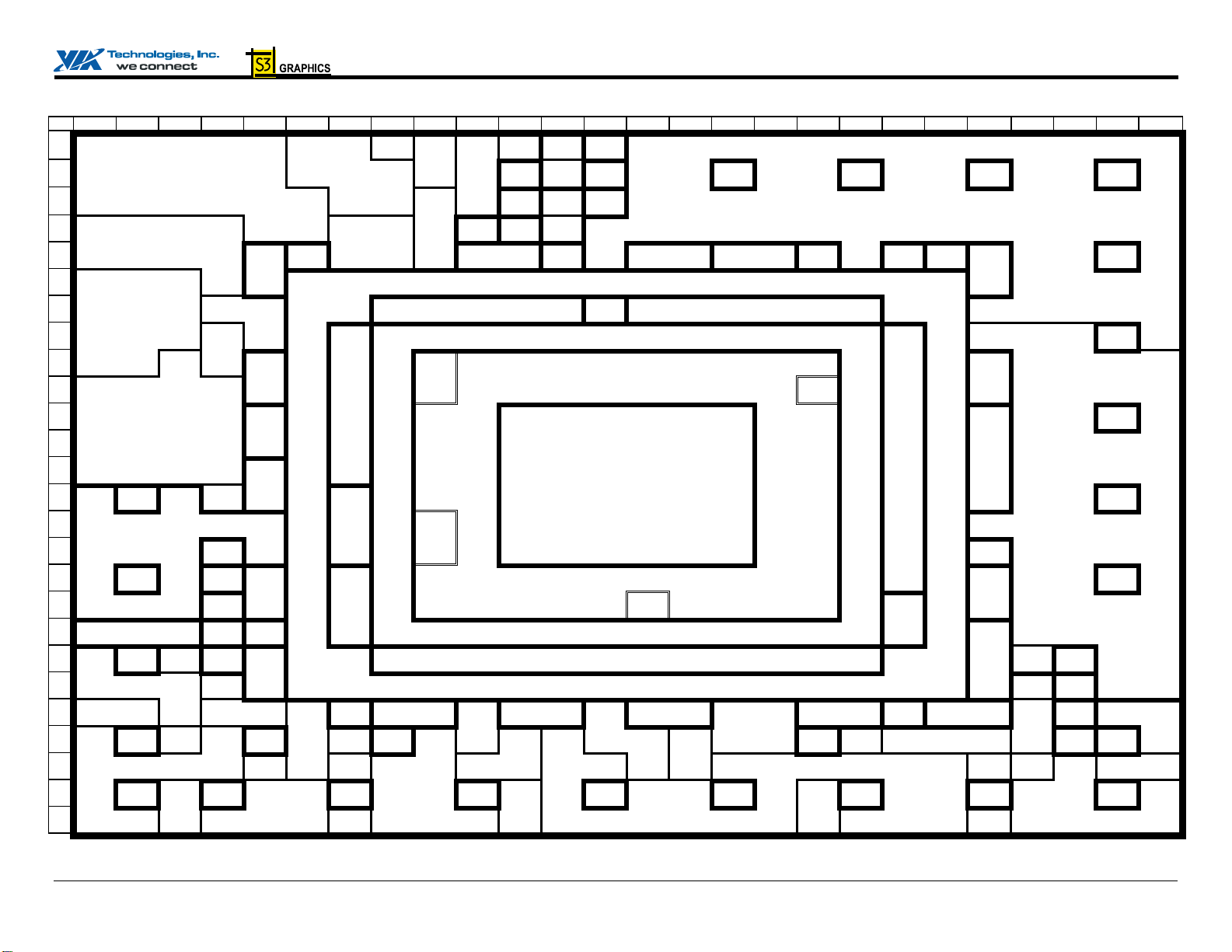
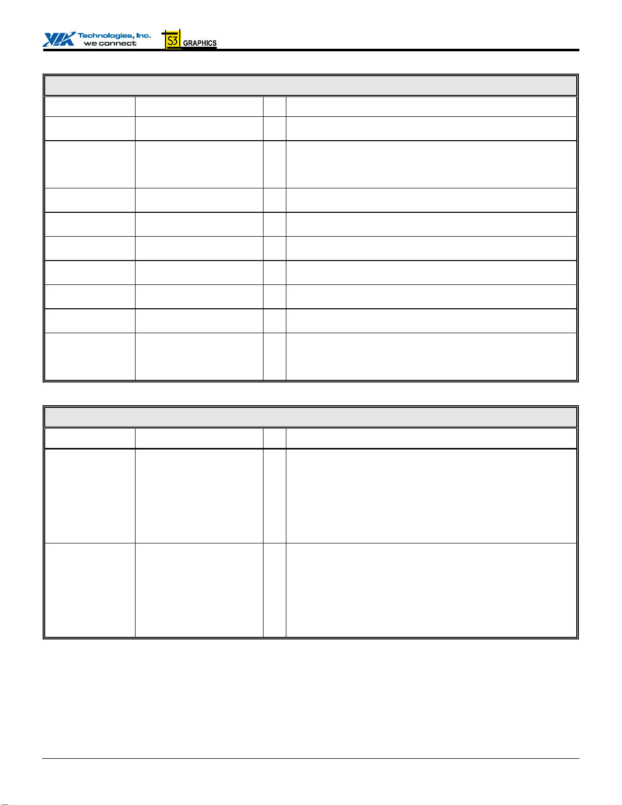
PINOUTS Figure 2. Ball Diagram (Top View)
Key 1 2 3 4 5 6 7 8 9 10 11 12 13 14 15 16 17 18 19 20 21 22 23 24 25 26
TVVS
TVD1
TVD3
TVD6
TVD9
DFT
A
DVIVS
DVID1
DVID3
DVID6
TVHS
TVD0
TVD2
B
DVIHS
DVID0
NC
TVCLK
C
DVIDT
CPD 3 CPD 2 CPD 1 CPD 0 TVBL#
D
CPD 5 CPD 4 CP
E
FPDE
F
CPD8
FPD2
G
CPD11
FPD5
H
CPD13
FPD7
J
CPD15
FPD10
K
DFDE
FPD15
L
DFD4
FPD18
M
DFD7
FPD21
N
DFD10
VAD
P
0
VAD 5 VDN
R
VUP
T
STB#
VAD
U
2
VAD 6 VAD 7 VAD 4 VL
V
PWR
W
OK
DVICLK
FPHS
CPHS
FPD1
CPD10
FPD4
CPD12
FPD6
CPD14
FPD9
DFHS
FPD14
DFD3
FPD17
DFD6
FPD22
DFD11
GND
STB
VUP
STB
GND
SUS
ST#
TVCKR
DFCLK
TVD5
DVID2
DVID5
TVD4
NC
DVID4
CLK
FPVS
CPVS
FPD0
CPD9
FPD3
DCLK I EN
CPCK1
FPCLK
DCLK
FPD8
FPD11
DFVS
DFD0
FPD13
FPD12
DFD2
DFD1
FPD19
FPD16
DFD8
DFD5
FPD20
FPD23
DFD9
DFDET
VAD 1 G
VDN
STB#
VDN
CMD
VREF
VL
PAR
COMP
RE
SET#
CPD 6 VCC
CPD 7 VCC
EN
VDD
O
CLK
VAD
3
VL
GND
CS3#
Y MD59 GND CS1# GND
AA MD63 MD58 MD62 CS0#
DQS
AB
7#
DQM
7
MD57
S
CAS# S WE#
DVID9
TVD8
DVID8
TVD7
DVID7
DVIDE
FP
FP
EN
VEE
BLT
GND
GND
VCC
FP
VCC
FP
GND
GND
VBE#
VUP
CMD
VCC
VL
VCC
VL
VSUS
25
VCC
M
VCC
M
TVD10
DVID10
TVD11
DVID11
AGP
IN
STDBY
INT
BIST
A#
AGP
SUSP
GPIO 0 GPIO 2 SP
GPIO 1 GPIO 3 SP
GND
F6 7 8 9 10 11 12 13 14 15 16 17 18 19 20 F21
G
VCC
H
VCC
J
VCC
K
VCC
L
VCC
M
VCC
N
VCC
P
VCC
R
VCC
T
VCC M VCC
U
VCC M VCC
V
VCC M VCC
W
Y
AA6 7 8 9 10 11 12 13 14 15 16 17 18 19 20 AA21
MA11
VREF
AC MD61 GND CS2# MD53 GND MA10 MD42 GND MD40 NC MA2 MD32 MA4 MA5
AD MD56 MD60 MD51 MD52
AE MD55 GND
AF MD50 MD54
DQS
GND MD47 MD46 GND MD41 MD39 GND
6#
DQM
MD49 MD48 MD43
6
S
RAS#
MA12
DQS
DQM
SP
CLK2 H SYNC
AGP
IN
BUSY#V SYNC
AGP
STP#
DAT2
DAT1
CLK1
VCC
FP
FP
FP
FP
FP
FP
VL
VL
VL
M
5#
5
VCC
FP
VCC
VCC
25
VCC
25
VCC
Panel
25
VCC
25
VCC
25
VCC
25
VCC
25
VCC
25
VCC
25
25
25
VCC
25
VCC M VCC M VCC M VCC M VCC M VCC M VCC M VCC M VCC M VCC M VCC M VCC
VCC M VCC
MD44 MD38 MA0 MA1 MD37 MD31 MA6
MD45 MD35 MD34
AB RSET
AG
SP
AR
VCC
RGB
GND GND XIN HD58 GND GND VTT VTT GND HD44
VCC
FP
FP
VCC
25
25
Flat
K10 11 12 13 14 15 16 K17
L
M
N
P
R
VL
Bus
T
U10 11 12 13 14 15 16 U17
DRAM
VCC
25
25
NC GND GND MA3 GND GND MA7 MA9
M
GND
GND
PLL1
GND
VCC
RGB
PLL1
VCC
GND
DAC
PLL2
GND
VCC
DAC
PLL2
VCC
VCC
FP
FP
VCC
VCC
25
25
GND GND GND GND GND GND
GND GND GND GND GND GND
GND GND GND GND GND GND
GND GND GND GND GND GND
GND GND GND GND GND GND
GND GND GND GND GND GND
VCC
VCC
25
25
DQM
MD33 GND MD30 MD25 GND MD22
4
DQS
MD36 MD27 MD26 MD29 MD28 MD19
4#
HD56 HD54 HD57 HD47 HD51 HD39 HD36 HD34 HD32 HD33 HD26 HD23 HD21
PLL3
GND HD61 HD55 GND HD40 HD49 GND HD37 HD22 GND HD19 HD24 GND HD16
VCC
HD60 HD46 HD52 HD63 HD41 HD45 HD38 HD28 HD31 HD25 HD30 HD7 HD3
PLL3
HD50 HD53 HD62 HD59 HD48 HD42 HD27 HD43 HD29 HD35 HD20 HD13 HD14 HD11
GND VTT VTT VTT VTT VTT VTT
VCC
VCC
VCC
25
VCC
25
25
VCC
25
VCC
25
25
VCC
VCC
25
25
DQM
MA8 MA13 GND MA14
3
DQS
MD24 MD23 MD18 MD17 MD11 MD10
3#
VCC
25
L
M
N
P
R
T
VCC
25
GTL
GND VTT HD2 HD9 GND HD18
VREF
VTT HD8 HD12 HD17 HD10
HD5 HD1 HD4 HD6 HD15
G
VCC
VCC
25
CPU
VCC
25
VCC M VCC M M
DQS
2#
DQM
2
VTT
25
VCC
VTT
25
VCC
VTT
25
VCC
VTT
25
VCC
VTT
25
VCC
VTT
25
VCC
VTT
25
VCC
VTT
25
VCC
VTT
25
VCC
VTT
25
VCC
VCC
25
M
VCC
VCC
25
M
M
GND MD16 MD14 GND MD12 MD8 GND MD6
MD21 MD20 MD15
VREF
CKE 0 CKE 2 CKE 1 MCLK
HA26 HA18
H
VTT HA29 HA24 HA27 HA30
J
VTT HA20 HA19 HA22 HA17
K
GND HA23 HA31 GND HA25
L
GND HA15 HA28 HA21 HA10
M
GND HA5 HA12 HA16 HA13
N
GND HA6 HA9 GND HA3
P
BNR# HA14 HA8 HA4 HA11
R
GTL
T
VREF
VTT
U
VTT
V
GND HIT#
W
GND
Y
GND MD0
VCC M VCC
MCLK
M
DQM 1 CKE
DQS
1#
CPU
RST#
HREQ
HA7
1#
DE
FER# H REQ0#
HIT
M# H REQ3#H LOCK#
D
BSY#
H
GND
CLK
HCK
VCC
HCK
VCC
MCK
GND
FB
MCK
MD2
3
MD13 MD9 MD3 MD7
GND HD0
HREQ
4# B PRI#
HT
H
REQ2#
RS1#
RS0#
D
RDY#
B
REQ0#
0#
GND
RDY#
RS2#
ADS#
MD5 MD4
GND MD1
DQM 0 DQS
Revision 2.06, December 1, 2004 -8- Pin Diagram
Page 15
CLE266 Version CD / CE North Bridge Data Sheet
K
K
K
Table 2. Pin List (Listed by Pin Number)
Pin # Pin Name Pin # Pin Name Pin # Pin Name Pin # Pin Name Pin # Pin Names Pin # Pin Name
A01 O TVVS / DVIVS D01 I CPD03 G19 P VTT P01 IO VAD0 / strap Y09 P VCCM AD01 IO MD56
A02 O TVD01 / DVID01 D02 I CPD02 G22 IO HD05 P02 P GND Y10 P VCCM AD02 IO MD60
A03 O TVD03 / DVID03 D03 I CPD01 G23 IO HD01 P03 IO VAD1 / strapY11 P VCCM AD03 IO MD51
A04 O TVD06 / DVID06 D04 I CPD00 G24 IO HD04 P04 I GCL
A05 O TVD09 / DVID09 D05 O TVBL# / DVIDE G25 IO HD06 P05 P GND Y13 P VCCM AD05 O SRAS#
A06 I DFTIN D06 O TVD11 / DVID11 G26 IO HD15 P07 P VCCVL Y14 P VCCM AD06 O MA12
A07 I AGPSTDBY D07 IO GPIO0 H01 O FPD05 / CPD13 P20 P VTT Y15 P VCCM AD07 O DQS5#
A08 IO SPCLK2 D08 IO GPIO2 H02 O FPD04 / CPD12 P22 P GND Y16 P VCCM AD08 IO MD44
A09 O HSYNC D09 IO SPDAT1 H03 O FPD03 / CPCK1 P23 IO HA06 Y17 P VCCM AD09 IO MD38
A10 O AB D10 P VCCRGB H04 I DCLKI P24 IO HA09 Y18 P VCCM AD10 O MA00
A11 A RSET D11 P GNDDAC H05 O ENBLT P25 P GND Y19 P VCCM AD11 O MA01
A12 P GNDPLL1 D12 P VCCPLL2 H07 P VCCFP P26 IO HA03 Y22 P GND AD12 IO MD37
A13 P GNDPLL3 D13 IO HD50 H20 P VTT R01 IO VAD5 Y23 I HCLK AD13 IO MD31
A14 IO HD56 D14 IO HD53 H22 IO HA26 R02 O VDNSTB Y24 P GNDHCK AD14 O MA06
A15 IO HD54 D15 IO HD62 H23 IO HA18 R03 O VDNSTB# Y25 IO RS2# AD15 O DQS3#
A16 IO HD57 D16 IO HD59 H24 O CPURST# R04 IO VAD3 / strapY26 IO DRDY# AD16 IO MD24
A17 IO HD47 D17 IO HD48 H25 P GND R05 IO VBE# AA01 IO MD63 AD17 IO MD23
A18 IO HD51 D18 IO HD42 H26 IO HD00 R07 P VCCVL AA02 IO MD58 AD18 IO MD18
A19 IO HD39 D19 IO HD27 J01 O FPD07 / CPD15 R20 P VTT AA03 IO MD62 AD19 IO MD17
A20 IO HD36 D20 IO HD43 J02 O FPD06 / CPD14 R22 IO BNR# AA04 O CS0# AD20 IO MD11
A21 IO HD34 D21 IO HD29 J03 O FPCLK / DFCL
A22 IO HD32 D22 IO HD35 J04 O DCLKO R24 IO HA08 AA22 P GND AD22 O DQM1
A23 IO HD33 D23 IO HD20 J05 P GND R25 IO HA04 AA23 IO MD00 AD23 O CKE3
A24 IO HD26 D24 IO HD13 J07 P VCCFP R26 IO HA11 AA24 P VCCHCK AD24 IO MD02
A25 IO HD23 D25 IO HD14 J20 P VTT T01 I VUPSTB# AA25 IO ADS# AD25 O DQM0
A26 IO HD21 D26 IO HD11 J22 P VTT T02 I VUPSTB AA26 O BREQ0# AD26 O DQS0#
B01 O TVHS / DVIHS E01 I CPD05 J23 IO HA29 T03 O VDNCMD AB01 O DQS7# AE01 IO MD55
B02 O TVD00 / DVID00 E02 I CPD04 J24 IO HA24 T04 P VLVREF AB02 O DQM7 AE02 P GND
B03 O TVD02 / DVID02 E03 I CPCLK J25 IO HA27 T05 I VUPCMD AB03 IO MD57 AE03 O DQS6#
B04 O TVD05 / DVID05 E04 I CPD06 J26 IO HA30 T07 P VCCVL AB04 O SCAS# AE04 P GND
B05 O TVD08 / DVID08 E05 P VCCFP K01 O FPD10 / DFDE / strapT20 P VTT AB05 O SWE# AE05 IO MD47
B06 O INTA# E06 P GND K02 O FPD09 / DFHS / strapT22 P GTLVREF AB06 O MA11 AE06 IO MD46
B07 I BISTIN E07 IO GPIO1 K03 O FPD08 / DFVS / strapT23 IO HREQ1# AB07 P MEMVREF AE07 P GND
B08 O AGPBUSY# E08 IO GPIO3 K04 O FPD11 / DFD00 / strapT24 IO HA07 AB08 P VCCM AE08 IO MD41
B09 O VSYNC E09 IO SPCLK1 K05 P GND T25 IO HREQ4# AB09 P VCCM AE09 IO MD39
B10 O AG E10 P GND K07 P VCCFP T26 IO BPRI# AB10 – NC AE10 P GND
B11 P GNDRGB E11 P GND K20 P VTT U01 IO VAD2 / strapAB11 P GND AE11 O DQM4
B12 P VCCPLL1 E12 I XIN K22 P VTT U02 P GND AB12 P GND AE12 IO MD33
B13 P GND E13 IO HD58 K23 IO HA20 U03 IO VLPAR AB13 O MA03 AE13 P GND
B14 IO HD61 E14 P GND K24 IO HA19 U04 P GND AB14 P GND AE14 IO MD30
B15 IO HD55 E15 P GND K25 IO HA22 U05 P VCCVL AB15 P GND AE15 IO MD25
B16 P GND E16 P VTT K26 IO HA17 U07 P VCCM AB16 O MA07 AE16 P GND
B17 IO HD40 E17 P VTT L01 O FPD15 / DFD04 / strapU20 P VTT AB17 O MA09 AE17 IO MD22
B18 IO HD49 E18 P GND L02 O FPD14 / DFD03 / strapU22 P VTT AB18 P VCCM AE18 O DQS2#
B19 P GND E19 IO HD44 L03 O FPD13 / DFD02 / strapU23 IO DEFER# AB19 P VCCM AE19 P GND
B20 IO HD37 E20 P GTLVREF L04 O FPD12 / DFD01 / strapU24 IO HREQ0# AB20 P MEMVREF AE20 IO MD16
B21 IO HD22 E21 P GND L05 P VCCFP U25 P GND AB21 P VCCM AE21 IO MD14
B22 P GND E22 P VTT L07 P VCCFP U26 IO HREQ2# AB22 P VCCM AE22 P GND
B23 IO HD19 E23 IO HD02 L20 P VTT V01 IO VAD6 AB23 O MCLK AE23 IO MD12
B24 IO HD24 E24 IO HD09 L22 P GND V02 IO VAD7 AB24 P VCCMCK AE24 IO MD08
B25 P GND E25 P GND L23 IO HA23 V03 IO VAD4 AB25 IO MD05 AE25 P GND
B26 IO HD16 E26 IO HD18 L24 IO HA31 V04 A VLCOMP AB26 IO MD04 AE26 IO MD06
C01 I DVIDET F01 O FPDE / CPD08 L25 P GND V05 P VCCVL AC01 IO MD61 AF01 IO MD50
C02 O TVCLK / DVICLK F02 O FPHS / CPHS L26 IO HA25 V07 P VCCM AC02 P GND AF02 IO MD54
C03 I TVCLKR / NC F03 O FPVS / CPVS M01 O FPD18 / DFD07 / strapV20 P VCCM AC03 O CS2# AF03 O DQM6
C04 O TVD04 / DVID04 F04 I CPD07 M02 O FPD17 / DFD06 / strapV22 P VTT AC04 IO MD53 AF04 IO MD49
C05 O TVD07 / DVID07 F05 P VCCFP M03 O FPD19 / DFD08 / strapV23 I HITM# AC05 P GND AF05 IO MD48
C06 O TVD10 / DVID10 F22 P VTT M04 O FPD16 / DFD05 / strapV24 IO HREQ3# AC06 O MA10 AF06 IO MD43
C07 I AGPSUSP F23 IO HD08 M05 P VCCFP V25 I HLOCK# AC07 IO MD42 AF07 O DQM5
C08 IO AGPSTP# F24 IO HD12 M07 P VCCFP V26 IO RS1# AC08 P GND AF08 IO MD45
C09 IO SPDAT2 F25 IO HD17 M20 P VTT W01 I PWRO
C10 O AR F26 IO HD10 M22 P GND W02 I SUSST# AC10 – NC AF10 IO MD34
C11 P VCCDAC G01 O FPD02 / CPD11 M23 IO HA15 W03 I RESET# AC11 O MA02 AF11 O DQS4#
C12 P GNDPLL2 G02 O FPD01 / CPD10 M24 IO HA28 W04 O CS3# AC12 IO MD32 AF12 IO MD36
C13 P VCCPLL3 G03 O FPD00 / CPD9 M25 IO HA21 W05 P VSUS25 AC13 O MA04 AF13 IO MD27
C14 IO HD60 G04 O ENVDD M26 IO HA10 W07 P VCCM AC14 O MA05 AF14 IO MD26
C15 IO HD46 G05 O ENVEE N01 O FPD21 / DFD10 / strapW20 P VCCM AC15 O DQM3 AF15 IO MD29
C16 IO HD52 G08 P VCCFP N02 O FPD22 / DFD11 / strapW22 P GND AC16 O MA08 AF16 IO MD28
C17 IO HD63 G09 P VCCFP N03 O FPD20 / DFD09 / strapW23 IO HIT# AC17 O MA13 AF17 IO MD19
C18 IO HD41 G10 P VCCFP N04 O FPD23 / DFDET W24 IO DBSY# AC18 P GND AF18 O DQM2
C19 IO HD45 G11 P VCCFP N05 P GND W25 IO HTRDY# AC19 O MA14 AF19 IO MD21
C20 IO HD38 G12 P VCCFP N07 P VCCFP W26 IO RS0# AC20 O CKE0 AF20 IO MD20
C21 IO HD28 G13 P GND N20 P VTT Y01 IO MD59 AC21 O CKE2 AF21 IO MD15
C22 IO HD31 G14 P VTT N22 P GND Y02 P GND AC22 O CKE1 AF22 O DQS1#
C23 IO HD25 G15 P VTT N23 IO HA05 Y03 O CS1# AC23 I MCLKFB AF23 IO MD13
C24 IO HD30 G16 P VTT N24 IO HA12 Y04 P GND AC24 P GNDMCK AF24 IO MD09
C25 IO HD07 G17 P VTT N25 IO HA16 Y05 P VCCM AC25 P GND AF25 IO MD03
C26 IO HD03 G18 P VTT N26 IO HA13 Y08 P VCCM AC26 IO MD01 AF26 IO MD07
Center VCC25 Pins (44 pins): H8-19, J8, 19, K8,19, L8,19, M8,19, N8,19, P8,19, R8,19, T8,19, V8,19, W8-19.
Center GND Pins (37 pins): G13, L11-16, M11-16, N11-16, P11-16, R11-16, T11-16
R23 IO HA14 AA05 P VCCM AD21 IO MD10
Y12 P VCCM AD04 IO MD52
AC09 IO MD40 AF09 IO MD35
Revision 2.06, December 1, 2004 -9- Pin Lists
Page 16
CLE266 Version CD / CE North Bridge Data Sheet
K
K
K
K
Table 3. Pin List (Listed by Pin Name)
Pin # Pin Name Pin # Pin Name Pin # Pin Name Pin # Pin Name Pin # Pin Names Pin # Pin Name
A10 O AB N01 O FPD21 / DFD10 / strap P24 IO HA09 A15 IO HD54 AC09 IO MD40 K07 P VCCFP
B10 O AG N02 O FPD22 / DFD11 / strapM26 IO HA10 B15 IO HD55 AE08 IO MD41 L05 P VCCFP
AA25 IO ADS# N04 O FPD23 / DFDET R26 IO HA11 A14 IO HD56 AC07 IO MD42 L07 P VCCFP
B08 O AGPBUSY# F01 O FPDE / CPD08 N24 IO HA12 A16 IO HD57 AF06 IO MD43 M05 P VCCFP
A07 I AGPSTDBY F02 O FPHS / CPHS N26 IO HA13 E13 IO HD58 AD08 IO MD44 M07 P VCCFP
C08 IO AGPSTP# F03 O FPVS / CPVS R23 IO HA14 D16 IO HD59 AF08 IO MD45 N07 P VCCFP
C07 I AGPSUSP P04 I GCLK M23 IO HA15 C14 IO HD60 AE06 IO MD46 AA24 P VCCHC
C10 O AR B13 P GND N25 IO HA16 B14 IO HD61 AE05 IO MD47 U07 P VCCM
B07 I BISTIN B16 P GND K26 IO HA17 D15 IO HD62 AF05 IO MD48 V07 P VCCM
R22 IO BNR# B19 P GND H23 IO HA18 C17 IO HD63 AF04 IO MD49 V20 P VCCM
T26 IO BPRI# B22 P GND K24 IO HA19 W23 IO HIT# AF01 IO MD50 W07 P VCCM
AA26 O BREQ0# B25 P GND K23 IO HA20 V23 I HITM# AD03 IO MD51 W20 P VCCM
AC20 O CKE0 E06 P GND M25 IO HA21 V25 I HLOCK# AD04 IO MD52 Y05 P VCCM
AC22 O CKE1 E10 P GND K25 IO HA22 U24 IO HREQ0# AC04 IO MD53 Y08 P VCCM
AC21 O CKE2 E11 P GND L23 IO HA23 T23 IO HREQ1# AF02 IO MD54 Y09 P VCCM
AD23 O CKE3 E14 P GND J24 IO HA24 U26 IO HREQ2# AE01 IO MD55 Y10 P VCCM
E03 I CPCLK E15 P GND L26 IO HA25 V24 IO HREQ3# AD01 IO MD56 Y11 P VCCM
D04 I CPD00 E18 P GND H22 IO HA26 T25 IO HREQ4# AB03 IO MD57 Y12 P VCCM
D03 I CPD01 E21 P GND J25 IO HA27 A09 O HSYNC AA02 IO MD58 Y13 P VCCM
D02 I CPD02 E25 P GND M24 IO HA28 W25 IO HTRDY# Y01 IO MD59 Y14 P VCCM
D01 I CPD03 G13 P GND J23 IO HA29 B06 O INTA# AD02 IO MD60 Y15 P VCCM
E02 I CPD04 H25 P GND J26 IO HA30 AD10 O MA00 AC01 IO MD61 Y16 P VCCM
E01 I CPD05 J05 P GND L24 IO HA31 AD11 O MA01 AA03 IO MD62 Y17 P VCCM
E04 I CPD06 K05 P GND Y23 I HCL
F04 I CPD07 L22 P GND H26 IO HD00 AB13 O MA03 AB07 P MEMVREF Y19 P VCCM
H24 O CPURST# L25 P GND G23 IO HD01 AC13 O MA04 AB20 P MEMVREF AA05 P VCCM
AA04 O CS0# M22 P GND E23 IO HD02 AC14 O MA05 AB10– NC AB08 P VCCM
Y03 O CS1# N05 P GND C26 IO HD03 AD14 O MA06 AC10– NC AB09 P VCCM
AC03 O CS2# N22 P GND G24 IO HD04 AB16 O MA07 W01 I PWROK AB18 P VCCM
W04 O CS3# P02 P GND G22 IO HD05 AC16 O MA08 W03 I RESET# AB19 P VCCM
W24 IO DBSY# P05 P GND G25 IO HD06 AB17 O MA09 W26 IO RS0# AB21 P VCCM
H04 I DCLKI P22 P GND C25 IO HD07 AC06 O MA10 V26 IO RS1# AB22 P VCCM
J04 O DCLKO P25 P GND F23 IO HD08 AB06 O MA11 Y25 IO RS2# AB24 P VCCMC
U23 IO DEFER# U02 P GND E24 IO HD09 AD06 O MA12 A11 A RSET B12 P VCCPLL1
A06 DFTIN U04 P GND F26 IO HD10 AC17 O MA13 AB04 O SCAS# D12 P VCCPLL2
AD25 O DQM0 U25 P GND D26 IO HD11 AC19 O MA14 E09 IO SPCLK1 C13 P VCCPLL3
AD22 O DQM1 W22 P GND F24 IO HD12 AC23 I MCLKFB A08 IO SPCLK2 D10 P VCCRGB
AF18 O DQM2 Y02 P GND D24 IO HD13 AB23 O MCL
AC15 O DQM3 Y04 P GND D25 IO HD14 AA23 IO MD00 C09 IO SPDAT2 R07 P VCCVL
AE11 O DQM4 Y22 P GND G26 IO HD15 AC26 IO MD01 AD05 O SRAS# T07 P VCCVL
AF07 O DQM5 AA22 P GND B26 IO HD16 AD24 IO MD02 W02 I SUSST# U05 P VCCVL
AF03 O DQM6 AB11 P GND F25 IO HD17 AF25 IO MD03 AB05 O SWE# V05 P VCCVL
AB02 O DQM7 AB12 P GND E26 IO HD18 AB26 IO MD04 D05 O TVBL# / DVIDE T03 O VDNCMD
AD26 IO DQS0# AB14 P GND B23 IO HD19 AB25 IO MD05 C02 O TVCLK / DVICLKR02 O VDNSTB
AF22 IO DQS1# AB15 P GND D23 IO HD20 AE26 IO MD06 C03 I TVCLKR R03 O VDNSTB#
AE18 IO DQS2# AC02 P GND A26 IO HD21 AF26 IO MD07 B02 O TVD00 / DVID00 V04 A VLCOMP
AD15 IO DQS3# AC05 P GND B21 IO HD22 AE24 IO MD08 A02 O TVD01 / DVID01 U03 IO VLPAR
AF11 IO DQS4# AC08 P GND A25 IO HD23 AF24 IO MD09 B03 O TVD02 / DVID02 T04 P VLVREF
AD07 IO DQS5# AC18 P GND B24 IO HD24 AD21 IO MD10 A03 O TVD03 / DVID03 W05 P VSUS25
AE03 IO DQS6# AC25 P GND C23 IO HD25 AD20 IO MD11 C04 O TVD04 / DVID04 B09 O VSYNC
AB01 IO DQS7# AE02 P GND A24 IO HD26 AE23 IO MD12 B04 O TVD05 / DVID05 E16 P VTT
Y26 IO DRDY# AE04 P GND D19 IO HD27 AF23 IO MD13 A04 O TVD06 / DVID06 E17 P VTT
C01 I DVIDET AE07 P GND C21 IO HD28 AE21 IO MD14 C05 O TVD07 / DVID07 E22 P VTT
H05 O ENBLT AE10 P GND D21 IO HD29 AF21 IO MD15 B05 O TVD08 / DVID08 F22 P VTT
G04 O ENVDD AE13 P GND C24 IO HD30 AE20 IO MD16 A05 O TVD09 / DVID09 G14 P VTT
G05 O ENVEE AE16 P GND C22 IO HD31 AD19 IO MD17 C06 O TVD10 / DVID10 G15 P VTT
J03 O FPCLK / DFCLK AE19 P GND A22 IO HD32 AD18 IO MD18 D06 O TVD11 / DVID11 G16 P VTT
G03 O FPD00 / CPD9 AE22 P GND A23 IO HD33 AF17 IO MD19 B01 O TVHS / DVIHS G17 P VTT
G02 O FPD01 / CPD10 AE25 P GND A21 IO HD34 AF20 IO MD20 A01 O TVVS / DVIVS G18 P VTT
G01 O FPD02 / CPD11 D11 P GNDDAC D22 IO HD35 AF19 IO MD21 P01 IO VAD0 / strap G19 P VTT
H03 O FPD03 / CPCK1 Y24 P GNDHCK A20 IO HD36 AE17 IO MD22 P03 IO VAD1 / strap H20 P VTT
H02 O FPD04 / CPD12 AC24 P GNDMCK B20 IO HD37 AD17 IO MD23 U01 IO VAD2 / strap J20 P VTT
H01 O FPD05 / CPD13 A12 P GNDPLL1 C20 IO HD38 AD16 IO MD24 R04 IO VAD3 / strap J22 P VTT
J02 O FPD06 / CPD14 C12 P GNDPLL2 A19 IO HD39 AE15 IO MD25 V03 IO VAD4 K20 P VTT
J01 O FPD07 / CPD15 A13 P GNDPLL3 B17 IO HD40 AF14 IO MD26 R01 IO VAD5 K22 P VTT
K03 O FPD08 / DFVS / strap B11 P GNDRGB C18 IO HD41 AF13 IO MD27 V01 IO VAD6 L20 P VTT
K02 O FPD09 / DFHS / strap D07 IO GPIO0 D18 IO HD42 AF16 IO MD28 V02 IO VAD7 M20 P VTT
K01 O FPD10 / DFDE / strap E07 IO GPIO1 D20 IO HD43 AF15 IO MD29 R05 IO VBE# N20 P VTT
K04 O FPD11 / DFD00 / strap D08 IO GPIO2 E19 IO HD44 AE14 IO MD30 C11 P VCCDAC P20 P VTT
L04 O FPD12 / DFD01 / strap E08 IO GPIO3 C19 IO HD45 AD13 IO MD31 E05 P VCCFP R20 P VTT
L03 O FPD13 / DFD02 / strap E20 P GTLVREF C15 IO HD46 AC12 IO MD32 F05 P VCCFP T20 P VTT
L02 O FPD14 / DFD03 / strap T22 P GTLVREF A17 IO HD47 AE12 IO MD33 G08 P VCCFP U20 P VTT
L01 O FPD15 / DFD04 / strap P26 IO HA03 D17 IO HD48 AF10 IO MD34 G09 P VCCFP U22 P VTT
M04 O FPD16 / DFD05 / strap R25 IO HA04 B18 IO HD49 AF09 IO MD35 G10 P VCCFP V22 P VTT
M02 O FPD17 / DFD06 / strap N23 IO HA05 D13 IO HD50 AF12 IO MD36 G11 P VCCFP T05 I VUPCMD
M01 O FPD18 / DFD07 / strap P23 IO HA06 A18 IO HD51 AD12 IO MD37 G12 P VCCFP T02 I VUPSTB
M03 O FPD19 / DFD08 / strap T24 IO HA07 C16 IO HD52 AD09 IO MD38 H07 P VCCFP T01 I VUPSTB#
N03 O FPD20 / DFD09 / strap R24 IO HA08 D14 IO HD53 AE09 IO MD39 J07 P VCCFP E12 I XIN
Center VCC25 Pins (44 pins): H8-19, J8,19, K8,19, L8,19, M8,19, N8,19, P8,19, R8,19, T8,19, V8,19, W8-19.
Center GND Pins (37 pins): G13, L11-16, M11-16, N11-16, P11-16, R11-16, T11-16
AC11 O MA02 AA01 IO MD63 Y18 P VCCM
D09 IO SPDAT1 P07 P VCCVL
Revision 2.06, December 1, 2004 -10- Pin Lists
Page 17
CLE266 Version CD / CE North Bridge Data Sheet
Pin Descriptions
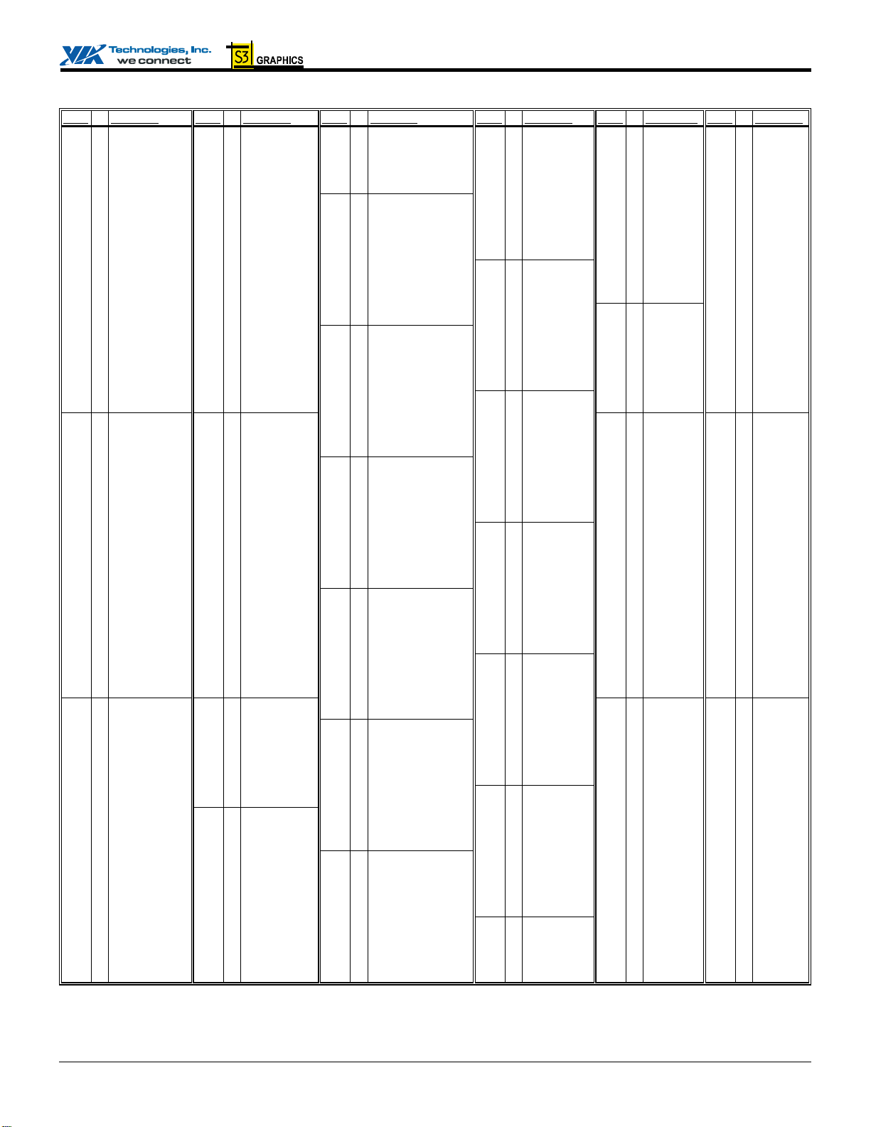
Table 4. Pin Descriptions
CPU Interface
Signal Name Pin # I/O Signal Description
HA[31:3]#
HD[63:0]#
ADS#
BNR#
BPRI#
DBSY#
DEFER#
DRDY#
HIT#
HITM#
HLOCK#
HREQ[4:0]#
HTRDY#
RS[2:0]#
CPURST#
BREQ0#
Note: Clocking of the CPU interface is performed with HCLK.
Note: Internal pullup resistors are provided on all GTL interface pins. If the CPU does not have internal pullups, the North
Bridge internal pullups may be enabled to allow the interface to meet GTL bus interface specifications (see strap
descriptions).
(see pin list) IO Host Address Bus. HA[31:3] connect to the address bus of the host CPU. During
CPU cycles HA[31:3] are inputs. These signals are driven by the CLE266 North Bridge
during cache snooping operations.
(see pin list) IO Host CPU Data. These signals are connected to the CPU data bus.
AA25 IO Address Strobe. The CPU asserts ADS# in T1 of the CPU bus cycle.
R22 IO Block Next Request. Used to block the current request bus owner from issuing new
requests. This signal is used to dynamically control the processor bus pipeline depth.
T26 IO Priority Agent Bus Request. The owner of this signal will always be the next bus
owner. This signal has priority over symmetric bus requests and causes the current
symmetric owner to stop issuing new transactions unless the HLOCK# signal is
asserted. The CLE266 North Bridge drives this signal to gain control of the processor
bus.
W24 IO Data Bus Busy. Used by the data bus owner to hold the data bus for transfers requiring
more than one cycle.
U23 IO Defer. A dynamic deferring policy is used to optimize system performance. The
DEFER# signal is also used to indicate a processor retry response.
Y26 IO Data Ready. Asserted for each cycle that data is transferred.
W23 IO Hit. Indicates that a caching agent holds an unmodified version of the requested line.
Also driven in conjunction with HITM# by the target to extend the snoop window.
V23 I Hit Modified. Asserted by the CPU to indicate that the address presented with the last
assertion of EADS# is modified in the L1 cache and needs to be written back.
V25 I Host Lock. All CPU cycles sampled with the assertion of HLOCK# and ADS# until
the negation of HLOCK# must be atomic.
T25, V24,
U26, T23,
U24
W25 IO Host Target Ready. Indicates that the target of the processor transaction is able to
Y25, V26, W26 IO Response Signals. Indicates the type of response per the table below:
H24 O CPU Reset. Reset output to CPU. External pullup and filter capacitor to ground
AA26 O Bus Request 0. Bus request output to CPU.
IO Request Command. Asserted during both clocks of the request phase. In the first
clock, the signals define the transaction type to a level of detail that is sufficient to
begin a snoop request. In the second clock, the signals carry additional information to
define the complete transaction type.
enter the data transfer phase.
RS[2:0]#
000 Idle State
001 Retry Response
010 Defer Response
011 Reserved
100 Hard Failure
101 Normal Without Data
110 Implicit Writeback
111 Normal With Data
should be provided per CPU manufacturer’s recommendations.
Response type
Revision 2.06, December 1, 2004 -11- Pin Description
Page 18
CLE266 Version CD / CE North Bridge Data Sheet
The pinouts were defined assuming the ATX PCB layout model shown below (and general pin layout shown) as a guide for PCB
component placement. Other PCB layouts (AT, LPX and NLX) were also considered and can typically follow the same general
component placement.
PCI Slots
VT8233A
South
Bridge
1 26
FP
Socket-370
CPU
CR
CPU
T
CLE
266
DRAM
A
…
AF
IDE Connectors
DRAM Modules
Power
Supply
V-Link Interface
Signal Name Pin # I/O Signal Description
VAD7,
VAD6,
VAD5,
VAD4,
VAD3 / strap,
VAD2 / strap,
VAD1 / strap,
VAD0 / strap
VLPAR
VBE#
VUPCMD
VUPSTB
VUPSTB#
VDNCMD
VDNSTB
VDNSTB#
V2
V1
R1
V3
R4
U1
P3
P1
U3 IO
R5 IO
T5 I
T2 I
T1 I
T3 O
R2 O
R3 O
IO
Address/Data Bus.
IO
IO
SB
Strap
IO
IO
IO
IO
IO
Function Setting (L=strap low, H=strap high) Register Pin
VAD3 GTL Pullup Enable L=Disable, H=Enable Rx50[6] SA19
VAD2 IOQ Depth L=1-Level, H=8-Level Rx50[7] SA18
VAD1 CPU FSB Clock Msb LL=66 MHz, LH=100 MHz Rx54[7] SA17
VAD0 CPU FSB Clock Lsb Hx=133 MHz Rx54[6] SA16
Parity.
Byte Enable.
Command from Client-to-Host.
Strobe from Client-to-Host.
Complement Strobe from Client-to-Host.
Command from Host-to-Client.
Strobe from Host-to-Client.
Complement Strobe from Host-to-Client.
Revision 2.06, December 1, 2004 -12- Pin Description
Page 19
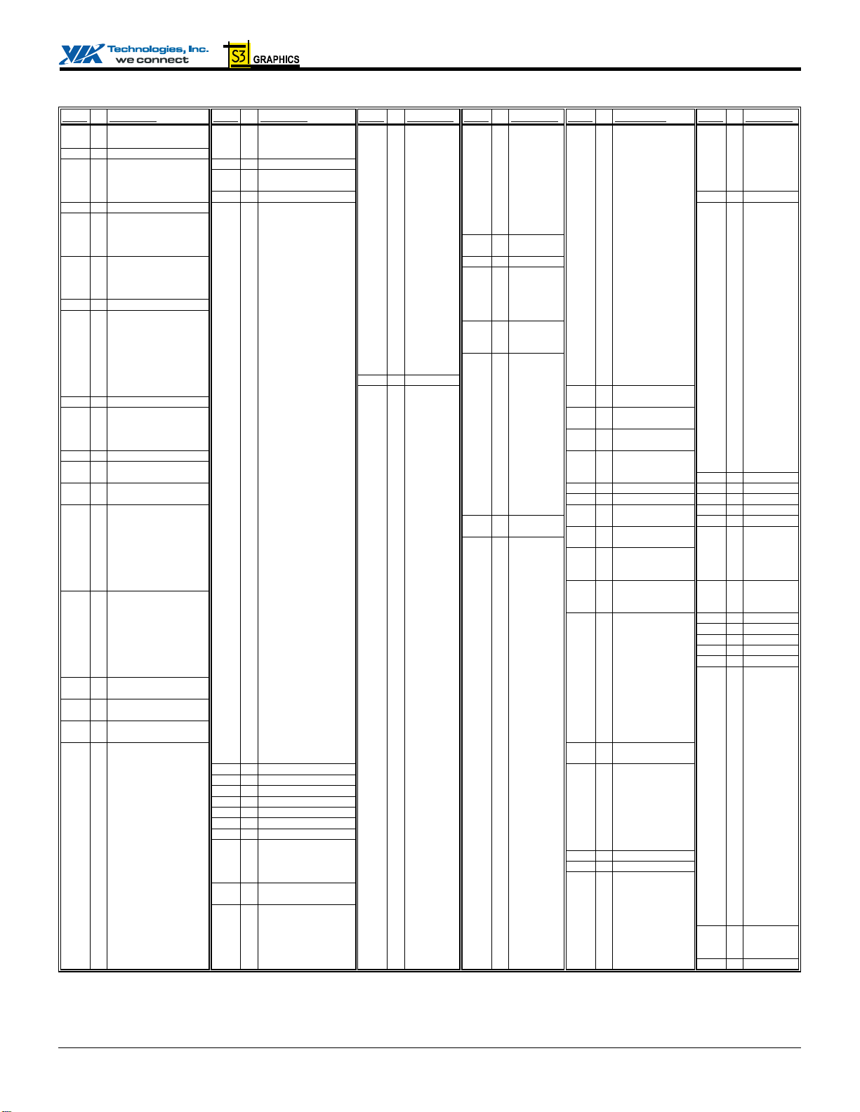
CLE266 Version CD / CE North Bridge Data Sheet
p
DDR Synchronous DRAM Memory Interface
Signal Name Pin # I/O Signal Description
MD[63:0]
MA[14-0]
CS[3:0]#
DQM[7:0]
DQS[7:0]# AB1, AE3, AD7, AF11,
SRAS#
SCAS#
SWE#
CKE[3:0]
(see pinout tables) IO Memory Data. These signals are connected to the DRAM data bus.
Output drive strength may be set by Device 0 Rx6D[1-0].
AC19, AC17, AD6, AB6,
AC6, AB17, AC16, AB16,
O Memory Address. DRAM address lines. Output drive strength may
be set by Device 0 Rx6C[7-6].
AD14, AC14, AC13, AB13,
AC11, AD11, AD10
W4, AC3, Y3, AA4 O Chip Select. Chip select of each bank. Output drive strength may be
set by Device 0 Rx6D[3-2].
AB2, AF3, AF7, AE11,
AC15, AF18, AD22, AD25
O Data Mask. Data mask of each byte lane. Output drive strength may
be set by Device 0 Rx6D[5-4].
IO DDR Data Strobe. Data strobe of each byte lane. Output drive
AD15, AE18, AF22, AD26
strength may be set by Device 0 Rx6C[3-2].
AD5 O Row Address Command Indicator. Output drive strength may be
set by Device 0 Rx6C[7-4].
AB4 O Column Address Command Indicator. Output drive strength may
be set by Device 0 Rx6C[7-4].
AB5 O Write Enable Command Indicator. Output drive strength may be
set by Device 0 Rx6C[7-4].
AD23, AC21, AC22, AC20 O Clock Enables. Clock enables for each DRAM bank for powering
down the SDRAM or clock control for reducing power usage and for
reducing heat / temperature in high-speed memory systems. See
Device 0 Rx6B[4].
SMB / I2C Interface
Signal Name Pin # I/O Signal Description
SPCLK[2:1]
SPDAT[2:1]
A8, E9 IO Serial Port (SMB/I2C) Clocks. These are the clocks for serial data
transfer. SPCLK1 is typically used for DDC communications with a
CRT monitor. As an output, it is programmed via CRA0[0]. As an
input, its status is read via CRA0[2]. In either case the serial port
must be enabled by CRA0[4] = 1. SPCLK2 is typically used for I
communications. As an output, it is programmed via CRB1[0]. As
an input, its status is read via CRB1[2]. The port is enabled via
CRB1[4] = 1.
C9, D9 IO Serial Port (SMB/I2C) Data. These are the data signals used for
serial data transfer. SPDAT1 is typically used for DDC
communications with a CRT monitor. As an output, it is
rogrammed via CRA0[1]. As an input, its status is read via
CRA0[3]. In either case the serial port must be enabled by CRA0[4]
= 1. SPDAT2 is typically used for I
output, it is programmed via CRB1[1]. As an input, its status is read
via CRB1[3]. The port is enabled via CRB1[4] = 1.
2
2
C communications. As an
C
Revision 2.06, December 1, 2004 -13- Pin Description
Page 20
CLE266 Version CD / CE North Bridge Data Sheet
Digital Monitor (DVI) Interface
Signal Name Pin # I/O Signal Description
DVID11 / TVD11,
DVID10 / TVD10,
DVID09 / TVD9,
DVID08 / TVD8,
DVID07 / TVD7,
DVID06 / TVD6,
DVID05 / TVD5,
DVID04 / TVD4,
DVID03 / TVD3,
DVID02 / TVD2,
DVID01 / TVD1,
DVID00 / TVD0
DVICLK / TVCLK C2 O Digital Monitor Clock Out. Internally pulled down during reset
DVIHS / TVHS B1 O Digital Monitor Horizontal Sync. Internally pulled down during reset
DVIVS / TVVS A1 O Digital Monitor Vertical Sync. Internally pulled down during reset
DVIDE / TVBL# D5 O Digital Monitor Display Enable. Indicates valid data on DVID[11:0]. Internally
DVIDET / NC C1 I Digital Monitor Detect. Rx?? will read 1 if a digital monitor is connected. Must be
D6
C6
A5
B5
C5
A4
B4
C4
A3
B3
A2
B2
O Digital Monitor Data Out. Internally pulled down during reset
pulled down during reset
tied to GND if not used.
TV Encoder Interface
Signal Name Pin # I/O Signal Description
TVD11 / DVID11,
TVD10 / DVID10,
TVD9 / DVID09,
TVD8 / DVID08,
TVD7 / DVID07,
TVD6 / DVID06,
TVD5 / DVID05,
TVD4 / DVID04,
TVD3 / DVID03,
TVD2 / DVID02,
TVD1 / DVID01,
TVD0 / DVID00
TVCLKR / NC C3 I TV Encoder Clock In. Input clock from encoder. Internally pulled down.
TVCLK / DVICLK C2 O TV Encoder Clock Out. Output clock to TV encoder. Internally pulled down.
TVHS / DVIHS B1 O TV Encoder Horizontal Sync. Internally pulled down during reset
TVVS / DVIVS A1 O TV Encoder Vertical Sync. Internally pulled down during reset
TVBL# / DVIDE D5 O TV Encoder Blanking. Internally pulled down during reset
D6
C6
A5
B5
C5
A4
B4
C4
A3
B3
A2
B2
O TV Encoder Data. Internally pulled down during reset
Revision 2.06, December 1, 2004 -14- Pin Description
Page 21
CLE266 Version CD / CE North Bridge Data Sheet
CRT Interface
Signal Name Pin # I/O Signal Description
AR
AB
AG
HSYNC
VSYNC
RSET
C10 A Analog Red. Analog red output to the CRT monitor.
A10 A Analog Blue. Analog blue output to the CRT monitor.
B10 A Analog Green. Analog green output to the CRT monitor.
A9 O Horizontal Sync. Output to CRT.
B9 O Vertical Sync. Output to CRT.
A11 A
Reference Resistor. Tie to GNDRGB through an external 147 Ω
control the RAMDAC full-scale current value.
± 1% resistor to
Direct LCD Panel Interface
Signal Name Pin # I/O Signal Description
Flat Panel Data Out. Bits 8-22 also function as strap inputs that are sampled on the
FPD23 / DFDET,
FPD22 / DFD11 / strap,
FPD21 / DFD10 / strap,
FPD20 / DFD09 / strap,
FPD19 / DFD08 / strap,
FPD18 / DFD07 / strap,
FPD17 / DFD06 / strap,
FPD16 / DFD05 / strap,
FPD15 / DFD04 / strap,
FPD14 / DFD03 / strap,
FPD13 / DFD02 / strap,
FPD12 / DFD01 / strap,
FPD11 / DFD00 / strap,
FPD10 / DFDE / strap,
FPD9 / DFHS / strap,
FPD8 / DFVS / strap,
FPD7 / CPD15,
FPD6 / CPD14,
FPD5 / CPD13,
FPD4 / CPD12,
FPD3 / CPCK1,
FPD2 / CPD11,
FPD1 / CPD10,
FPD0 / CPD09
FPVS / CPVS F3 O Flat Panel Vertical Sync. Internally pulled down.
FPHS / CPHS F2 O Flat Panel Horizontal Sync. Internally pulled down.
FPDE / CPD08 F1 O Flat Panel Data Enable. Internally pulled down.
FPCLK / DFCLK J3 O Flat Panel Clock. Internally pulled down during reset.
ENVDD
ENVEE
ENBLT
N4
N2
N1
N3
M3
M1
M2
M4
L1
L2
L3
L4
K4
K1
K2
K3
J1
J2
H1
H2
H3
G1
G2
G3
G4 O Enable VDD. This signal is driven high to initiate a flat panel power up sequence.
G5 O Enable VEE. This signal is driven high for a programmable time after ENVDD is
H5 O
O
rising edge of RESET#. These straps are defined per the table below. “L” indicates
O
strap low (4.7KΩ to ground), “H” = strap high (4.7KΩ to 10KΩ t 3.3V). See Design
O
Guide for details.
O
O
Strap
O
O
O
O
O
O
O
O
O
O
O
O
O
O
O
O
O
O
O
Function Setting Register
FPD22 Reserved for Test Always Strap Low –
FPD21-20 TV Mode LL=PAL, LH=NTSC, EXSR13[4:3]
HL=PAL-N, HH=PAL-NC
FPD19 TV # of Lines L=525 Lines, H=625 Lines EXSR12[6]
FPD18 DVI Port Configuration L=DVI, H=TV EXSR12[5]
FPD17 Panel Interface Config L=DVI / Capture, H=Panel EXSR12[4]
FPD16-13 Panel Type Customer Defined (contact VIA) EXSR12[3:0]
FPD12 Reserved for Test Always Strap Low –
FPD11 Reserved for Test Always Strap Low –
FPD10 Reserved for Test Always Strap Low –
FPD9 Reserved for Test Always Strap Low –
FPD8 Reserved for Test Always Strap Low –
driven high during a flat panel power up sequence.
Enable Backlight.
Revision 2.06, December 1, 2004 -15- Pin Description
Page 22
CLE266 Version CD / CE North Bridge Data Sheet
Video Capture Interface
Signal Name Pin # I/O Signal Description
I
CPD15 / FPD7,
CPD14 / FPD6,
CPD13 / FPD5
CPD12 / FPD4,
CPD11 / FPD2,
CPD10 / FPD1,
CPD09 / FPD0
CPD08 / FPDE
CPD07
CPD06
CPD05
CPD04
CPD03
CPD02
CPD01
CPD00
CPVS / FPVS F3 I Video Capture Vertical Sync. Internally pulled down.
CPHS / FPHS F2 I Video Capture Horizontal Sync. Internally pulled down.
CPCLK
CPCK1 / FPD3 H3 I Video Capture Clock 1. Clock for capture data inputs 8-15 when used as a second 8-bit
Note: The Video Capture Port may always be used in 8-bit input mode. The “upper” data bits (CPD[15:8] may be used as a 16-bit
extension or as a second 8-bit port if the 24-bit direct flat panel interface is not used.
J1
J2
H1
H2
G1
G2
G3
F1
F4
E4
E1
E2
D1
D2
D3
D4
E3 I Video Capture Clock 0. Clock for capture data inputs 0-7 (or 0-15 when capture port is
Flat Panel Data Out.
configured as 16-bit)
capture port.
Alternate Digital Monitor (DVI) Interface
Signal Name Pin # I/O Signal Description
O
DFD11 / FPD22,
DFD10 / FPD21,
DFD09 / FPD20,
DFD08 / FPD19,
DFD07 / FPD18,
DFD06 / FPD17,
DFD05 / FPD16,
DFD04 / FPD15,
DFD03 / FPD14,
DFD02 / FPD13,
DFD01 / FPD12,
DFD00 / FPD11
DFCLK / FPCLK J3 O Digital Monitor Clock. Internally pulled down during reset.
DFHS / FPD9 K2 O Digital Monitor Horizontal Sync. Internally pulled down during reset
DFVS / FPD8 K3 O Digital Monitor Vertical Sync. Internally pulled down during reset
DFDE / FPD10 K1 O Digital Monitor Display Enable. Indicates valid data on DFD[11:0]. Internally pulled down
DFDET / FPD23 N4 O Digital Monitor Detect. Rx?? will read 1 if a digital monitor is connected. Must be tied to
Note: All “DFxxx” pins perform the same function as the “DMxxx” pins (the other DVI interface muxed with the TV-out pins).
N2
N1
N3
M3
M1
M2
M4
L1
L2
L3
L4
K4
Digital Monitor Data Out.
during reset
GND if not used.
Revision 2.06, December 1, 2004 -16- Pin Description
Page 23
CLE266 Version CD / CE North Bridge Data Sheet
b
p
Clocks, Resets, Power Control, General Purpose I/O, Interrupts and Test
Signal Name Pin # I/O Signal Description
HCLK
MCLK
MCLKFB
DCLKI
DCLKO
XIN
RESET#
PWROK
SUSST#
INTA#
AGPBUSY#
GPIO0
GPIO1
GPIO2
GPIO3
AGPSTOP#
AGPSTDBY
AGPSUSP
GCLK
BISTIN
DFTIN
NC
Y23 I Host Clock. This pin receives the host CPU clock (100 / 133 MHz). This clock is
used by all CLE266 logic that is in the host CPU domain.
AB23 O Memory (SDRAM) Clock. Output from the internal clock generator to the
external clock buffer.
AC23 I Memory (SDRAM) Clock Feedback. Input from the external clock buffer.
H4 I Dot Clock (Pixel Clock) In. Used for external EMI reduction circuit if used.
Loop back from DCLKO if external EMI reduction circuit not implemented.
J4 O Dot Clock (Pixel Clock) Out. Used for external EMI reduction circuit if used.
Loop back to DCLKI if external EMI reduction circuit not implemented.
E12 I Reference Frequency Input. 14.31818 MHz reference clock input for the internal
graphics controller Phase Locked Loops (PLLs). All internal graphics controller
clocks are synthesized on chip using this frequency as a reference.
W3 I Reset. When asserted low, this signal resets the internal logic of the chip and sets
all register bits to their default values. The rising edge of this signal is used to
sample all power-up strap options. Normally driven by the South Bridge.
W1 I Power OK. When asserted high, this signal indicates that system voltages are
correct and stable. Driven by onthe chipset South Bridge.
W2 I Suspend Status. For implementation of the Suspend-to-DRAM feature.
Normally driven by the South Bridge. Connect to an external pullup if not used.
B6 O Interrupt. PCI interrupt output (handled by the interrupt controller in the South
Bridge)
B8 O AGP Interface Busy. Connect to a South Bridge GPIO pin for monitoring the
status of the internal AGP bus. See CLE266 Design Guide for details.
D7 O
E7 O
D8 O
E8 O
C8 I AGP Stop. Assert low to stop the internal AGP interface (for power measurement
A7 I AGP Standby. Assert high to put the internal AGP interface into standby mode
C7 I AGP Suspend. Assert high to put the internal AGP interface into suspend mode
P4 I Graphics Clock. 66 MHz clock from system clock synthesizer.
B7 I BIST (Built-In-Self-Test) In. This
A6 I DFT (Design-For-Test) In. This pin is used for testing and must be tied low on
AB10, AC10 – No Connect. Do not connect. Reserved for future use.
General Purpose Input / Output 0.
General Purpose Input / Output 1.
General Purpose Input / Output 2.
General Purpose Input / Output 3.
only, not used in normal operation)
(for power measurement only, not used in normal operation)
(for power measurement only, not used in normal operation)
all board designs.
all board designs.
oard Power Good circuitry. Also connected to
in is used for testing and must be tied low on
Revision 2.06, December 1, 2004 -17- Pin Description
Page 24
CLE266 Version CD / CE North Bridge Data Sheet
Power, Ground and Test
Signal Name Pin # I/O Signal Description
VTT
GTLVREF
VCCM
MEMVREF
VCCVL
VLCOMP
VLVREF
VCC25
VSUS25
VCCHCK
VCCMCK
VCCFP
VCCRGB
VCCDAC
VCCPLL1
VCCPLL2
VCCPLL3
GND
GNDHCK
GNDMCK
GNDRGB
GNDDAC
GNDPLL1
GNDPLL2
GNDPLL3
(see pin list) P Power for CPU I/O Interface Logic. Voltage is CPU dependent. See CLE266
Design Guide for details.
E20, T22 P CPU Interface GTL+ Voltage Reference. 2/3 VTT ±2% typically derived using a
resistive voltage divider. See CLE266 Design Guide for details.
(see pin list) P Power for Memory I/O Interface Logic. 2.5 ±5%.
AB7, AB20 P
P7, R7, T7, U5, V5 P Power for V-Link I/O Interface Logic. 2.5V ±5%.
V4 I V-Link P-Channel Compensation. Connect 70 Ω 1% resistor to ground.
T4 P V-Link Voltage Reference. 0.9V derived using a resistive voltage divider between
(see pin list) P Power for Internal Digital Logic. 2.5V ±5%.
W5 P Suspend Power. 2.5V ±5%.
AA24 P Power for Host CPU Clock DLL. 2.5V ±5%.
AB24 P Power for Memory Clock DLL. 2.5V ±5%.
(see pin table) P Power for Flat Panel, DVI, TV-Out and Video Capture Interfaces. 3.3V ±5%.
D10 P Power for CRT RGB Outputs. 2.5V ±5%.
C11 P Power for DAC Digital Logic. 2.5V ±5%.
B12 P Power for Graphics Controller PLL 1. 2.5V ±5%.
D12 P Power for Graphics Controller PLL 2. 2.5V ±5%.
C13 P Power for Graphics Controller PLL 3. 2.5V ±5%.
(see pin table) P Ground for Internal Digital Logic. Connect to primary PCB ground plane.
Y24 P Ground for Host CPU Clock Circuitry. Connect to main ground plain through a
AC24 P Ground for Memory Clock Circuitry. Connect to main ground plain through a
B11 P
D11 P
A12 P
C12 P
A13 P
Memory Voltage Reference.
VCC25 and ground (see Design Guide for details).
ferrite bead.
ferrite bead.
Connection Point for RGB Load Resistors.
Ground for DAC Digital Circuitry.
Ground for Graphics Controller PLL 1.
Ground for Graphics Controller PLL 2.
Ground for Graphics Controller PLL 3.
Revision 2.06, December 1, 2004 -18- Pin Description
Page 25

CLE266 Version CD / CE North Bridge Data Sheet
REGISTERS
Register Overview
The following tables summarize the configuration and I/O
registers. These tables also document the power-on default
value (“Default”) and access type (“Acc”) for each register.
Access type definitions used are RW (Read/Write), RO
(Read/Only), “—” for reserved / used (essentially the same as
RO) and RWC (or just WC) (Read / Write 1’s to Clear
individual bits). Registers indicated as RW may have some
read/only bits that always read back a fixed value (usually 0 if
unused); registers designated as RWC or WC may have some
read-only or read write bits (see individual register
descriptions following these tables for details). All offset and
default values are shown in hexadecimal unless otherwise
indicated.
Table 5. Registers
I/O Ports
Port #
I/O Port Default Acc
0022 PCI / AGP Arbiter Disable 00 RW
0CFB-0CF8 Configuration Address 0000 0000 RW
0CFF-0CFC Configuration Data 0000 0000 RW
Revision 2.06, December 1, 2004 -19- Register Overview
Page 26

CLE266 Version CD / CE North Bridge Data Sheet
Device 0 Registers - Host Bridge
Header Registers
Offset Configuration Space Header Default Acc
1-0 Vendor ID
3-2 Device ID
5-4 Command
7-6 Status
8 Revision ID
9 Program Interface 00 RO
A Sub Class Code 00 RO
B Base Class Code
C -reserved- 00 —
D Latency Timer 00
E Header Type 00 RO
F Built In Self Test (BIST) 00 RO
13-10 Graphics Aperture Base
14-2B -reserved- 00 —
2D-2C Subsystem Vendor ID 0000
2F-2E Subsystem ID 0000
30-33 -reserved- 00 —
34 Capability Pointer
35-3F -reserved- 00 —
Device-Specific Registers
Offset V-Link Control Default Acc
40 V-Link Revision ID 00
41 V-Link NB Capability
42 V-Link NB Downlink Command
44-43 V-Link NB Uplink Status
45 V-Link NB Bus Timer
46 V-Link Misc NB Control 00 RW
47 V-Link Control 00 RW
48 V-Link NB/SB Configuration
49 V-Link SB Capability
4A V-Link SB Downlink Status
4C-4B V-Link SB Uplink Command
4D V-Link SB Bus Timer
4E CCA Master High Priority 00 RW
4F V-Link SB Miscellaneous Control 00 RW
Offset Host CPU Protocol Control Default Acc
50 CPU Interface Request Phase Control
51 CPU Interface Basic Control 00 RW
52 CPU Interface Advanced Control 00 RW
53 CPU Interface Arbitration Control
54 CPU Miscellaneous Control 00 RW
1106
3123
0006 RW
0210 WC
0n
06
0000 0008 RW
A0
18 RO
88
8280 RO
44
18
18
88 RO
8280
44
20
03
RO
RO
RO
RO
RW
W1
W1
RO
RO
RW
RW
RW
RW
RW
RW
RW
RW
Device-Specific Registers (continued)
Offset DRAM Control Default Acc
55 DRAM Control 00 RW
56-57 -reserved- 00 —
58 MA Map Type
59 -reserved- 00 —
5F-5A DRAM Row Ending Address:
5A Bank 0 Ending (HA[31:24])
5B Bank 1 Ending (HA[31:24])
5C Bank 2 Ending (HA[31:24])
5D Bank 3 Ending (HA[31:24])
5E-5F -reserved-
60 DRAM Type 00 RW
61 ROM Shadow Control C0000-CFFFF 00 RW
62 ROM Shadow Control D0000-DFFFF 00 RW
63 ROM Shadow Control E0000-FFFFF 00 RW
64 DRAM Timing for All Banks
65 DRAM Arbitration Timer 00 RW
66 DRAM Arbitration Control 00 RW
67 DRAM DQS/SDR/MD Read Delay 00 RW
68 DRAM DDR Control 00 RW
69 Extended SMRAM Control 00 RW
6A DRAM Refresh Counter 00 RW
6B DRAM Arbitration Control 00 RW
6C SDRAM Control 00 RW
6D DRAM Control Drive Strength 00 RW
6E-6F -reserved- 00 —
Offset PCI Bus Control Default Acc
70 PCI Buffer Control 00 RW
71 CPU to PCI Flow Control
72 -reserved- 00 —
73 PCI Master Control 1 00 RW
74 -reserved- 00 —
75 PCI Arbitration 1 00 RW
76 PCI Arbitration 2 00 RW
77-7F -reserved- 00 —
22
01
01
01
01
01
E4
48
RW
RW
RW
RW
RW
RW
RW
RW
Revision 2.06, December 1, 2004 -20- Register Summary Tables
Page 27

CLE266 Version CD / CE North Bridge Data Sheet
Device 0 Device-Specific Registers (continued)
Offset GART/TLB Control Default Acc
83-80 GART/TLB Control 0000 0000 RW
84 Graphics Aperture Size 00 RW
85 Write Policy 00 RW
86-87 -reserved- 00 —
8B-88 Gr. Aperture TLB Base Register Base 0000 0000 RW
8C-9F -reserved- 00 —
Offset AGP Control Default Acc
A0 AGP ID
A1 AGP Next Item Pointer
A2 AGP Specification Revision
A3 -reserved- 00 —
A7-A4 AGP Status
AB-A8 AGP Command 0000 0000 RW
AC AGP Control 00 RW
AD AGP Miscellaneous Control 1
AE AGP Miscellaneous Control 2 00 RW
AF-B3 -reserved- 00 —
Offset V-Link Control Default Acc
B4 V-Link NB Compensation Control 00 RW
B5 V-Link NB Drive Control 00 RW
B6-B7 -reserved- 00 —
B8 V-Link SB Compensation Control 00 RW
B9 V-Link SB Drive Control 00 RW
BA-BB -reserved- 00 —
02 RO
C0 RO
20 RO
1F00 0207 RO
02
RW
Device 0 Device-Specific Registers (continued)
Offset Power Management Control Default Acc
BC Power Management Mode 00 RW
BD DRAM Power Management 00 RW
BE Dynamic Clock Stop 00 RW
BF MA / SCMD Pad Toggle Reduction 00 RW
C0 Power Management Capability
C1 Power Management Next Pointer 00
C2 Power Management Capabilities I 02
C3 Power Management Capabilities II 00
C4 Power Management Control/Status 00 RW
C5 Power Management Status 00 RW
C6 PCI-to-PCI Bridge Support Extension 00 RW
C7 Power Management Data 00 RW
C8-DF -reserved- 00 —
Offset Frame Buffer & High Memory Ctrl Default Acc
E0 CPU Direct Access FB Base 00 RW
E1 CPU Direct Access FB Size 00 RW
E2 VGA Arbitration Timer 1 00 RW
E3 UMA Control 00 RW
E4-E5 -reserved- 00 —
E6 SMM / APIC Decoding
E7 -reserved- 00 —
E8 VGA Arbitration Timer 2
E9-EF -reserved- 00 —
Offset Test, BIOS Scratch, Miscellaneous Default Acc
F7-F0 BIOS Scratch Registers 00 RW
F8-FB -reserved- 00 —
FC-FF Reserved (Do Not Program) 0000 RW
01 RO
RO
RO
RO
01
40
RW
RW
Revision 2.06, December 1, 2004 -21- Register Summary Tables
Page 28

CLE266 Version CD / CE North Bridge Data Sheet
Device 1 Registers - PCI-to-PCI Bridge
Header Registers
Offset Configuration Space Header Default Acc
1-0 Vendor ID
3-2 Device ID
5-4 Command
7-6 Status
8 Revision ID
9 Programming Interface 00 RO
A Sub Class Code
B Base Class Code
C -reserved- 00 —
D Latency Timer 00 RO
E Header Type
F -reserved- (Built In Self Test) 00 —
10-17 -reserved- 00 —
18 Primary Bus Number 00
19 Secondary Bus Number 00
1A Subordinate Bus Number 00
1B Secondary Latency Timer 00 RO
1C I/O Base
1D I/O Limit 00
1F-1E Secondary Status 0000 RO
21-20 Memory Base
23-22 Memory Limit (Inclusive) 0000
25-24 Prefetchable Memory Base
27-26 Prefetchable Memory Limit 0000
28-33 -reserved- 00 —
34 Capability Pointer
35-3D -reserved- 00 —
3F-3E PCI-to-PCI Bridge Control 0000
1106
B091
0007 RW
0230 WC
0n
04
06
01
F0 RW
FFF0 RW
FFF0 RW
80
RO
RO
RO
RO
RO
RO
RW
RW
RW
RW
RW
RW
RO
RW
Device-Specific Registers
Offset AGP Bus Control Default Acc
40 CPU-to-AGP Flow Control 1 00 RW
41 CPU-to-AGP Flow Control 2
42 AGP Master Control 00 RW
43 AGP Master Latency Timer
44 Reserved (Do Not Program)
45 Fast Write Control
47-46 PCI-to-PCI Bridge Device ID 0000 RW
48 AGP Parity Error Control 00 RW
49-7F -reserved- 00 —
Offset Power Management Default Acc
80 Capability ID
81 Next Pointer 00
82 Power Management Capabilities 1
83 Power Management Capabilities 2 00
84 Power Management Control / Status 00 RW
85 Power Management Status 00
86 PCI-PCI Bridge Support Extensions 00
87 Power Management Data 00
88-FF -reserved- 00 —
08
22
20
72
01 RO
02 RO
RW
RW
RW
RW
RO
RO
RO
RO
RO
Revision 2.06, December 1, 2004 -22- Register Summary Tables
Page 29

CLE266 Version CD / CE North Bridge Data Sheet
Graphics Controller Registers
PCI Configuration Space Header Registers
Offset
Configuration Space Header Default Acc
1-0 Vendor ID
3-2 Device ID
5-4 Command
7-6 Status
8 Revision ID
9 Program Interface 00 RO
A Sub Class Code 00 RO
B Base Class Code
C -reserved- 00 —
D Latency Timer 00 RO
E Header Type 00 RO
F Built In Self Test (BIST) 00 RO
13-10 Memory Base 0
17-14 Memory Base 1 0000 0000
18-2B -reserved- 00 —
2D-2C Subsystem Vendor ID 0000 RO
2F-2E Subsystem ID 0000 RO
30-33 -reserved- 00 —
34 Capability Pointer
35-3B -reserved- 00 —
3C Interrupt Line 00
3D Interrupt Pin
3E-3F -reserved- 00 —
1106
3122
0000 RW
0230 WC
0n
03
0000 0008 RW
60
01 RW
RO
RO
RO
RO
RW
RO
RW
Memory Base 0
Up to 64 MB for the graphics and video playback buffer.
Memory Base 1
16 MB for memory mapped I/O, 2D host Bitblt space and
burst command area.
Offset Range Memory Mapped I/O (0 to 2M-1) Acc
0000-01FF 2D Engine Control RW
0200-03FF Video-related Engines Control RW
0400-07FF 3D Engine Control RW
0800-0BFF Burst Command Area RW
0C00-0DFF DVD Engine (MPEG) Control RW
0E00-0FFF DMA / AGP Control RW
1000-83BF -reserved- —
83Cx-83Dx VGA Memory Mapped I/O RW
83E0-FFFF -reserved- —
Offset Range 2D Host Bitblt / Burst Command Area Acc
2M to 4M-1 2D Host Bitblt Space RW
4M to 8M-1 Burst Command Area RW
8M to 16M-1 -reserved- —
PCI Configuration Space Device-Specific Registers
Offset
Power Management Configuration Default Acc
40-5F -reserved- 00 —
60 Capability ID
61 Next Item Pointer
63-62 Power Management Capabilities
65-64 Power Management Control / Status 0000 RW
67-66 Data + PM Control / Status BSE 0000
68-6F -reserved- 00 —
AGP Configuration Default Acc
Offset
70 Capability ID
71 Next Item Pointer 00
73-72 Revision Number
77-74 AGP Status
7B-78 AGP Command 0000 0000 RW
7C-FF -reserved- 00 —
01 RO
70 RO
0622 RO
RO
02 RO
RO
0020 RO
1F00 0207 RO
Revision 2.06, December 1, 2004 -23- Register Summary Tables
Page 30

CLE266 Version CD / CE North Bridge Data Sheet
VGA Registers
Port Index General Registers Acc
3C2 - Miscellaneous Output
3CC - Miscellaneous Output
3C2 - Input Status 0
3?A - Input Status 1
3C3 - Video Subsystem Enable RW
46E8 - Video Adapter Enable RW
In the port column above "?" = B for monochrome mode and
D for color mode.
Port Index Attribute Controller Registers Acc
3C0 - Index RW
3C1 00-0F Color Palette RW
3C1 10 Mode Control RW
3C1 11 Overscan Color RW
3C1 12 Color Plane Enable RW
3C1 13 Horizontal Pixel Panning RW
3C1 14 Color Select RW
3C1 15-7F -reserved- —
Port Index Sequencer Registers Acc
3C4 - Index RW
3C5 00 Reset RW
3C5 01 Clocking Mode RW
3C5 02 Map Mask RW
3C5 03 Character Map Select RW
3C5 04 Memory Mode RW
3C5 05-0F -reserved- —
3C5 10-7F
Port Index Graphics Controller Registers Acc
3CE - Index RW
3CF 00 Set / Reset RW
3CF 01 Set / Reset Enable RW
3CF 02 Color Compare RW
3CF 03 Data Rotate RW
3CF 04 Read Map Select RW
3CF 05 Mode RW
3CF 06 Miscellaneous RW
3CF 07 Color Don't Care RW
3CF 08 Bit Mask RW
3CF 09-1F -reserved- —
3CF 20-7F
Refer to any VGA book or technical reference for detailed
descriptions of the bits of the above VGA-standard registers.
(extended registers - see next page)
(extended registers - see next page)
WO
RO
RO
RO
Port Index CRT Controller Registers Acc
3?4 - Index RW
3?5 00 Horizontal Total RW
3?5 01 Horizontal Display End RW
3?5 02 Start Horizontal Blank RW
3?5 03 End Horizontal Blank RW
3?5 04 Start Horizontal Retrace RW
3?5 05 End Horizontal Retrace RW
3?5 06 Vertical Total RW
3?5 07 Overflow RW
3?5 08 Preset Row Scan RW
3?5 09 Max Scan Line RW
3?5 0A Cursor Start RW
3?5 0B Cursor End RW
3?5 0C Start Address High RW
3?5 0D Start Address Low RW
3?5 0E Cursor Location High RW
3?5 0F Cursor Location Low RW
3?5 10 Vertical Retrace Start RW
3?5 11 Vertical Retrace End RW
3?5 12 Vertical Display End RW
3?5 13 Offset RW
3?5 14 Underline Location RW
3?5 15 Start Vertical Blank RW
3?5 16 End Vertical Blank RW
3?5 17 CRTC Mode Control RW
3?5 18 Line Compare RW
3?5 19-31 -reserved- —
3?5 32-7F
In the port column above "?" = B for monochrome mode and
D for color mode.
Refer to any VGA book or technical reference for detailed
descriptions of the bits of the above VGA-standard registers.
(extended registers - see next page)
Revision 2.06, December 1, 2004 -24- Register Summary Tables
Page 31

CLE266 Version CD / CE North Bridge Data Sheet
VGA Extended Registers
Port Index Extended Sequencer Registers Acc
3C5 10 Extended Register Unlock RW
3C5 11 Configuration 0
3C5 12 Configuration 1
3C5 13 Configuration 2
3C5 14 Memory Clock DPA 0 RW
3C5 15 Display Mode Control RW
3C5 16 Display FIFO Threshold Control RW
3C5 17 Display FIFO Control RW
3C5 18 Display Arbitor Control 0 RW
3C5 19 Clock Control RW
3C5 1A PCI Bus Control RW
3C5 1B Power Management Control 0 RW
3C5 1C Horiz Display Quadword Count Data RW
3C5 1D Horiz Display Quadword Count Control RW
3C5 1E Power Management Control RW
3C5 1F Memory Control 0 RW
3C5 20 Typical Arbiter Control 0 RW
3C5 21 Typical Arbiter Control 1 RW
3C5 22 Display Arbiter Control 1 RW
3C5 23 Memory Control 1 RW
3C5 24 Memory Control 2 RW
3C5 25 General Purpose I/O Port RW
3C5 26 IIC Serial Port Control 0 RW
3C5 27 Memory Control 3 RW
3C5 28 Memory Control 4 RW
3C5 29 Memory Control 5 RW
3C5 2A MCK De-skew Control 0 RW
3C5 2B MCK De-skew Control 1 RW
3C5 2C General Purpose I/O Port RW
3C5 2D Power Management Control 1 RW
3C5 2E Power Management Control 2 RW
3C5 2F PCI Config Memory Base Shadow 0 RW
3C5 30 PCI Config Memory Base Shadow 1 RW
3C5 31 IIC Serial Port Control 1 RW
3C5 32 SPR 1 RW
3C5 33 SPR 2 RW
3C5 34 SPR 3 RW
3C5 36-35 Subsystem Vender ID RW
3C5 38-37 Subsystem ID RW
3C5 3A-39 BIOS Reserved Register 1-0 RW
3C5 3F-3B -reserved- —
3C5 40 AGP Pad Control 1 RW
3C5 41 Typical Arbitor Control 1 RW
3C5 42 Typical Arbitor Control 2 RW
3C5 43 -reserved- —
(“3C5” Sequencer Extended Registers table continued at top
of next column)
RO
RO
RO
Port Index Extended Sequencer Regs (continued) Acc
3C5 44 LCDCK Clock Synth D Value (def=C3h) RW
3C5 45 LCDCK Clock Synth N Value (def=2Ah) RW
3C5 46 VCK Clock Synthesizer D Value (C3h) RW
3C5 47 VCK Clock Synthesizer N Value (2Ah) RW
3C5 48 ECK Clock Synthesizer D Value (47h) RW
3C5 49 ECK Clock Synthesizer N Value (6Ah) RW
3C5 4A MCK Clock Synthesizer D Value RW
3C5 4B MCK Clock Synthesizer N Value RW
3C5 4C-7F -reserved- —
Port Index Extended Graphics Controller Regs Acc
3CF 20 Offset Register Control RW
3CF 21 Offset Register A RW
3CF 22 Offset Register B RW
3CF 23-7F -reserved- —
Port Index Extended CRT Controller Regs Acc
3?5 32 Mode Control RW
3?5 33 HSYNC Adjuster RW
3?5 34 Starting Address Overflow RW
3?5 35 Extended Overflow RW
3?5 36 Power Mgmt Control 3 (Monitor Control) RW
3?5 37 -reserved- —
3?5 38 Signature Data Register B0 RW
3?5 39 Signature Data Register B1 RW
3?5 3A Signature Data Register B2 RW
3?5 3F-3B BIOS Reserved Register 6-2 RW
3?5 40 Test Mode Control 0 RW
3?5 41-45 -reserved- —
3?5 46 Test Mode Control 1 RW
3?5 47 Test Mode Control 2 RW
3?5 48 Test Mode Control 3 RW
3?5 49-7F -reserved- —
Revision 2.06, December 1, 2004 -25- Register Summary Tables
Page 32

CLE266 Version CD / CE North Bridge Data Sheet
2D Graphics Engine Registers
Offset 2D Graphics Engine Registers Acc
0000 GE Command RW
0004 GE Mode / Status RW
0008 BitBLT Source Address RW
000C BitBLT Destination Address RW
0010 Dimension RW
0014 Pattern Address RW
0018 FG Color or Destination Color Key RW
001C BG Color or Source Color Key RW
0020 Scissors Top and Left Limit RW
0024 Scissors Bottom and Right Limit RW
0028 Offset RW
002C Direct3D Control RW
0030 Source Map Base Address RW
0034 Destination Map Base Address RW
0038 Pitch RW
003C Mono Pattern Data Port 0 WO
0040 Mono Pattern Data Port 1 WO
0044 -reserved- —
0100-01FF Color Pattern RAM Ports 0-63 WO
All registers above are 32-bit memory mapped with offsets
relative to Memory Base 1.
Revision 2.06, December 1, 2004 -26- Register Summary Tables
Page 33

CLE266 Version CD / CE North Bridge Data Sheet
Video Engine Registers
Offset Video Playback & Blending Registers Acc
0200 Interrupt Flags & Masks Control RW
0204 Ram Table & Address Flip Status
0208 Alpha Win & HI H & V Start RW
020C Alpha Win H & V End & HI Center Offset RW
0210 Alpha Window Control RW
0214 CRT Starting Address RW
0218 Second Display Start Address RW
021C Alpha Stream Frame Buffer Stride RW
0220 CRT Color Key RW
0224 Alpha Win & HI FB Start Address RW
0228 Chroma Key Lower Bound RW
022C Chroma Key Upper Bound RW
0230 Video Stream 1 Control RW
0234 Video Win 1 Fetch Count. RW
0238 Video Win 1 FB Y Start Address 1 RW
023C Video Win 1 FB Stride RW
0240 Video Win 1 H & V Start RW
0244 Video Win 1 H & V End RW
0248 Video Win 1 FB Y Start Address 2 RW
024C Video Win 1 Display Zoom Control RW
0250 Video Win 1 Minify & Interpolation Ctrl RW
0254 Video Win 1 FB Y Start Address 0 RW
0258 Video 1 FIFO Depth / Threshold Control RW
025C Video Win 1 FB Y Start Address 3 RW
0260 HI Control RW
0264 Second Display Color Key RW
0268 V3 & Alpha Win FIFO Depth & Thr Ctrl RW
026C V1 Source Image Line Count RW
0270 HI Transparent Color RW
0274 V1 Display Temporary Zoom Control RW
0278 V3 & Alpha Win FIFO Depth / Thr Ctrl RW
027C, 0280 -reserved- —
0284 V1 CSC & Enhancement Control (I) RW
0288 V1 CSC & Enhancement Control (II) RW
028C V1 FB U Start Address 0 RW
0290, 0294 -reserved- —
0298 Compose Outputs Mode Select RW
029C -reserved- —
02A0 V3 Control RW
02A4 V3 Frame Buffer Starting Address 0 RW
02A8 V3 Frame Buffer Starting Address 1 RW
02AC V3 Frame Buffer Stride RW
02B0 V3 Horizontal and Vertical Start RW
02B4 V3 Horizontal and Vertical End RW
02B8 V3 & Alpha Window Fetch Count RW
02BC V3 Display Zoom Control 1 RW
02C0 V3 Minify & Interpolation Control RW
02C4 V3 CSC & Enhancement Control (I) RW
02C8 V3 CSC & Enhancement Control (II) RW
02CC V3 Display Temporary Zoom Control RW
RO
Offset Video Playback & Blending Regs (cont) Acc
02D0 Graphics Hardware Cursor Mode Control RW
02D4 Graphics Hardware Cursor Position RW
02D8 Graphics Hardware Cursor Origin RW
02DC Graphics Hardware Cursor FG Color RW
02E0 Graphics Hardware Cursor BG Color RW
02E4 Video Window 1 FB U Start Address 1 RW
02E8 Video Window 1 FB U Start Address 2 RW
02EC Video Window 1 FB U Start Address 3 RW
02F0 Video Window 1 FB V Start Address 0 RW
02F4 Video Window 1 FB V Start Address 1 RW
02F8 Video Window 1 FB V Start Address 2 RW
02FC Video Window 1 FB V Start Address 3 RW
All registers above are 32-bit memory mapped with offsets
relative to Memory Base 1. FG = Foreground, BG =
Background, Win = Window, FB = Frame Buffer, CSC =
Color Space Conversion, Thr = Threshold
Revision 2.06, December 1, 2004 -27- Register Summary Tables
Page 34

CLE266 Version CD / CE North Bridge Data Sheet
Video Engine Registers (continued)
Offset Video Capture Engine & HQV Regs Acc
0300 C0 Interrupt Flags and Masks Control RW
0304 C1 Interrupt Flags and Masks Control RW
0308, 030C -reserved- —
0310 C0 Interface Control RW
0314 C0 Video H Range (CCIR601 only) RW
0318 C0 Video V Range (CCIR601 only) RW
031C C0 Scaling Control RW
0320 C0 VBI Data Horizontal Range RW
0324 C0 VBI Data Vertical Range RW
0328 C0 VBI Memory Starting Address RW
032C C0 VBI Memory Stride RW
0330 C0 Ancillary Data Count Setting RW
0334 C0 Max Count of Active Video Data RW
0338 C0 Max VBI or ANC Memory Data Count RW
033C C0 Capture Data Count
0340 C0 Video Capture Data 1st FB Start Addr RW
0344 C0 Video Capture Data 2nd FB Start Addr RW
0348 C0 Video Capture Data 3rd FB Start Addr RW
034C -reserved- —
0350 C0 Active Video Data Memory Stride &
Coring Function
0354 C1 Interface Control RW
0358-377 -reserved- —
0378 C1 Max Count of Active Video Data RW
037C -reserved- —
0380 C1 Capture Data Count RW
0384 C1 Video Capture Data 1st FB Start Addr RW
0388 C1 Video Capture Data 2nd FB Start Addr RW
038C C1 Active Video Data Memory Stride &
Coring function
0390-3BF -reserved- —
03C0 Sub-picture FB Stride & Control RW
03C4 Sub-picture FB Start Address RW
03C8 Sub-picture 4 X 16 RAM Table Write Ctrl RW
03CC Sub-picture RAM Table Read Data
03D0 HQV Stream Control / Status RW
03D4 HQV SW Source Data Start Address 0 (Y) RW
03D8 HQV SW Source Data Start Address 1 (U) RW
03DC HQV SW Source Data Start Address 2 (V) RW
03E0 HQV Source Data Line Count & Fetch
Count Per Line
03E4 HQV Filter Control RW
03E8 HQV Minify Control RW
03EC HQV Destination Data Start Address 0 RW
03F0 HQV Destination Data Start Address 1 RW
03F4 HQV Destination FB Stride RW
03F8 HQV Source FB Stride RW
03FC -reserved- —
All registers above are 32-bit memory mapped with offsets
relative to Memory Base 1. FB = Frame Buffer, C0 = Capture
0, C1 = Capture 1, HQV = High Quality Video, VBI =
Vertical Blanking Interval
RO
RW
RW
RO
RW
3D Engine Registers
Offset 3D Graphics Engine Registers Acc
(see CLE266 graphics programming manual for details)
All registers above are 32-bit memory mapped with offsets
relative to Memory Base 1.
Revision 2.06, December 1, 2004 -28- Register Summary Tables
Page 35

CLE266 Version CD / CE North Bridge Data Sheet
DVD Engine Registers
Offset DVD Engine (MPEG) Regs Default Acc
0C00 Picture Description 0000 0000 RW
0C04 Macroblock Description 0000 0000 RW
0C08 Null xxxx xxxx
0C0C MPEG Control 0000 0000 RW
0C10 Motion Vector 0 xxxx xxxx
0C14 Motion Vector 1 xxxx xxxx
0C18 Motion Vector 2 xxxx xxxx
0C1C Motion Vector 3 xxxx xxxx
0C20 Buffer 0 Y Base Address xxxx xxxx
0C24 Buffer 0 Cb Base Address xxxx xxxx
0C28 Buffer 0 Cr Base Address xxxx xxxx
0C2C Buffer 1 Y Base Address xxxx xxxx
0C30 Buffer 1 Cb Base Address xxxx xxxx
0C34 Buffer 1 Cr Base Address xxxx xxxx
0C38 Buffer 2 Y Base Address xxxx xxxx
0C3C Buffer 2 Cb Base Address xxxx xxxx
0C40 Buffer 2 Cr Base Address xxxx xxxx
0C44 Buffer 3 Y Base Address xxxx xxxx
0C48 Buffer 3 Cb Base Address xxxx xxxx
0C4C Buffer 3 Cr Base Address xxxx xxxx
0C50 Line Offset xxxx xxxx
0C54 MPEG Decoder Status xxxx xxxx RW
0C58 IDCT Block Data xxxx xxxx
0C5C Quantizer Matrix Selection xxxx xxxx
0C60 Quantizer Matrix Content xxxx xxxx
0C64 Slice Bit Stream Content xxxx xxxx
0C80-0C8C IDCT Coefficients / Datum xxxx xxxx
0C90 Slice Control 1 xxxx xxxx
0C94 Slice Control 2 xxxx xxxx
0C98 Slice Control 3 xxxx xxxx
0C9C Slice Control 4 xxxx xxxx
0CA0 Slice Bit Stream xxxx xxxx
0CA4-0DFF -reserved- — —
All registers above are 32-bit memory mapped with offsets
relative to Memory Base 1.
W
W
W
W
W
W
W
W
W
W
W
W
W
W
W
W
W
W
W
W
W
R
W
W
W
W
W
W
DMA Controller Registers
Offset DMA Controller Registers Default Acc
0E00-0E3F -reserved- — —
0E40 Channel 0 Memory Address 0000 0000 RW
0E44 Channel 0 Device Address 0000 0000 RW
0E48 Channel 0 Byte Count 0000 0000 RW
0E4C Channel 0 Descriptor Pointer 0000 0000 RW
0E50 Channel 1 Memory Address 0000 0000 RW
0E54 Channel 1Device Address 0000 0000 RW
0E58 Channel 1Byte Count 0000 0000 RW
0E5C Channel 1Descriptor Pointer 0000 0000 RW
0E60 Channel 2 Memory Address 0000 0000 RW
0E64 Channel 2 Device Address 0000 0000 RW
0E68 Channel 2 Byte Count 0000 0000 RW
0E6C Channel 2 Descriptor Pointer 0000 0000 RW
0E70 Channel 3 Memory Address 0000 0000 RW
0E74 Channel 3 Device Address 0000 0000 RW
0E78 Channel 3 Byte Count 0000 0000 RW
0E7C Channel 3 Descriptor Pointer 0000 0000 RW
0E80 Channel 0 Mode 0000 0000 RW
0E84 Channel 1 Mode 0000 0000 RW
0E88 Channel 2 Mode 0000 0000 RW
0E8C Channel 3 Mode 0000 0000 RW
0E90 Channel 0 Command / Status 0000 0000 RW
0E94 Channel 1 Command / Status 0000 0000 RW
0E98 Channel 2 Command / Status 0000 0000 RW
0E9C Channel 3 Command / Status 0000 0000 RW
0EA0 Priority Type 0000 0000 RW
0EA4-0FFF -reserved- — —
All registers above are 32-bit memory mapped with offsets
relative to Memory Base 1. Channels 2 and 3 are currently
reserved.
Revision 2.06, December 1, 2004 -29- Register Summary Tables
Page 36

CLE266 Version CD / CE North Bridge Data Sheet
Miscellaneous I/O
One I/O port is defined: Port 22.
Port 22 – PCI / AGP Arbiter Disable ..............................RW
7-2 Reserved ........................................ always reads 0
1 AGP Arbiter Disable
0 Respond to GREQ# signal .....................default
1 Do not respond to GREQ# signal
0 PCI Arbiter Disable
0 Respond to all REQ# signals..................default
1 Do not respond to any REQ# signals,
including PREQ#
This port can be enabled for read/write access by setting bit-7
of Device 0 Configuration Register 78.
PCI Configuration Space I/O
All registers (listed above in the “register summary” section of
this document) are addressed via the following configuration
mechanism:
Mechanism #1
These ports respond only to double-word accesses. Byte or
word accesses will be passed on unchanged.
Port CFB-CF8 - Configuration Address......................... RW
31 Configuration Space Enable
0 Disabled................................................. default
1 Convert configuration data port writes to
30-24 Reserved ........................................always reads 0
23-16 PCI Bus Number
Used to choose a specific PCI bus in the system
15-11 Device Number
Used to choose a specific device in the system
10-8 Function Number
Used to choose a specific function if the selected
7-2 Register Number (also called the "Offset")
Used to select a specific DWORD in the
1-0 Fixed ........................................always reads 0
configuration cycles on the PCI bus
(devices 0 and 1 are defined)
device supports multiple functions (only function 0 is
defined).
configuration space
Port CFF-CFC - Configuration Data.............................. RW
Refer to PCI Bus Specification Version 2.2 for further details
on operation of the above configuration registers.
Revision 2.06, December 1, 2004 -30- Miscellaneous and Configuration Space I/O
Page 37

CLE266 Version CD / CE North Bridge Data Sheet
Device 0 Register Descriptions
Device 0 Host Bridge Header Registers
All registers are located in PCI configuration space. They
should be programmed using PCI configuration mechanism 1
through 0CF8 / 0CFC with bus number, function number and
device number
Device 0 Offset 1-0 - Vendor ID (1106h) ..........................RO
15-0 ID Code (reads 1106h to identify VIA Technologies)
Device 0 Offset 3-2 - Device ID (3123h)............................RO
15-0 ID Code (reads 3123h to identify the CLE266 North
Device 0 Offset 5-4 –Command (0006h).......................... RW
15-10 Reserved ........................................ always reads 0
9 Fast Back-to-Back Cycle Enable ........................RO
0 Fast back-to-back transactions only allowed to
1 Fast back-to-back transactions allowed to
8 SERR# Enable......................................................RO
0 SERR# driver disabled ...........................default
1 SERR# driver enabled
(SERR# is used to report ECC errors)
7 Address / Data Stepping......................................RO
0 Device never does stepping....................default
1 Device always does stepping
6 Parity Error Response........................................ RW
0 Ignore parity errors & continue..............default
1 Take normal action on detected parity errors
5 VGA Palette Snoop..............................................RO
0 Treat palette accesses normally..............default
1 Don’t respond to palette accesses on PCI bus
4 Memory Write and Invalidate Command .........RO
0 Bus masters must use Mem Write..........default
1 Bus masters may generate Mem Write & Inval
3 Special Cycle Monitoring ....................................RO
0 Does not monitor special cycles.............default
1 Monitors special cycles
2 PCI Bus Master....................................................RO
0 Never behaves as a bus master
1 Can behave as a bus master...................default
1 Memory Space......................................................RO
0 Does not respond to memory space
1 Responds to memory space...................default
0 I/O Space ..........................................................RO
0 Does not respond to I/O space ..............default
1 Responds to I/O space
equal to zero.
Bridge chip)
the same agent........................................default
different agents
Device 0 Offset 7-6 – Status (0210h)............................. RWC
15 Detected Parity Error
0 No parity error detected......................... default
1 Error detected in either address or data phase.
This bit is set even if error response is disabled
(command register bit-6).....write one to clear
14 Signaled System Error (SERR# Asserted)
........................................always reads 0
13 Signaled Master Abort
0 No abort received .................................. default
1 Transaction aborted by the master ...................
..................................write one to clear
12 Received Target Abort
0 No abort received .................................. default
1 Transaction aborted by the target .....................
..................................write one to clear
11 Signaled Target Abort .......................always reads 0
0 Target Abort never signaled
10-9 DEVSEL# Timing
00 Fast
01 Medium ................................. always reads 01
10 Slow
11 Reserved
8 Data Parity Error Detected
0 No data parity error detected ................. default
1 Error detected in data phase. Set only if error
response enabled via command bit-6 = 1 and
The CLE266 was initiator of the operation in
which the error occurred
..................................write one to clear
7 Fast Back-to-Back Capable ...............always reads 0
6 User Definable Features.....................always reads 0
5 66MHz Capable .................................. always reads 0
4 Supports New Capability list........... always reads 1
3-0 Reserved ........................................always reads 0
Device 0 Offset 8 - Revision ID (0nh)............................... RO
7-0 Chip Revision Code........................always reads 0nh
Device 0 Offset 9 - Programming Interface (00h)........... RO
7-0 Interface Identifier.........................always reads 00h
Device 0 Offset A - Sub Class Code (00h)........................ RO
7-0 Sub Class Code.......reads 00 to indicate Host Bridge
Device 0 Offset B - Base Class Code (06h)....................... RO
7-0 Base Class Code.. reads 06 to indicate Bridge Device
Device 0 Offset D - Latency Timer (00h) ........................ RW
Specifies the latency timer value in PCI bus clocks.
7-3 Guaranteed Time Slice for CPU ............... default=0
2-0 Reserved (fixed granularity of 8 clks).. always read 0
Bits 2-1 are writeable but read 0 for PCI specification
compatibility. The programmed value may be read
back in Offset 75 bits 5-4 (PCI Arbitration 1).
Revision 2.06, December 1, 2004 -31- Device 0 Register Descriptions
Page 38

CLE266 Version CD / CE North Bridge Data Sheet
Device 0 Host Bridge Header Registers (continued)
Device 0 Offset E - Header Type (00h).............................RO
7-0 Header Type Code ............. reads 00: single function
Device 0 Offset F - Built In Self Test (BIST) (00h)..........RO
7 BIST Supported .......reads 0: no supported functions
6-0 Reserved ........................................ always reads 0
Device 0 Offset 13-10 - Graphics Aperture Base
(00000008h) .......................................................................RW
31-28 Upper Programmable Base Address Bits ...... def=0
27-20 Lower Programmable Base Address Bits ...... def=0
These bits behave as if hardwired to 0 if the
corresponding Graphics Aperture Size register bit
(Device 0 Offset 84h) is 0.
27 26 25 24 23 22 21 20 (This Register)
7
RW RW RW RW RW RW RW RW 1M
RW RW RW RW RW RW RW 0 2M
RW RW RW RW RW RW 0 0 4M
RW RW RW RW RW 0 0 0 8M
RW RW RW RW 0 0 0 0 16M
RW RW RW 0 0 0 0 0 32M
RW RW 0 0 0 0 0 0 64M
RW 0 0 0 0 0 0 0 128M
0 0 0 0 0 0 0 0 256M
6 5 4 3 2 1 0 (Gr Aper Size)
Device 0 Host Bridge Header Registers (continued)
Device 0 Offset 2D-2C – Subsys Vendor ID (0000h)... W1/R
15-0 Subsystem Vendor ID .............................. default = 0
This register may be written once and is then read only.
Device 0 Offset 2F-2E – Subsystem ID (0000h)........... W1/R
15-0 Subsystem ID ............................................default = 0
This register may be written once and is then read only.
Device 0 Offset 34 - Capability Pointer (A0h)................. RO
Contains a byte offset from the start of configuration space.
7-0 AGP Capability List Pointer ........always reads A0h
19-0 Reserved ................................ always reads 00008
Note: The locations in the address range defined by this
register are prefetchable.
Revision 2.06, December 1, 2004 -32- Device 0 Register Descriptions
Page 39

CLE266 Version CD / CE North Bridge Data Sheet
Device 0 Host Bridge Device-Specific Registers
These registers are normally programmed once at system
initialization time.
V-Link Control
Device 0 Offset 40 – V-Link Specification ID (00h).........RO
7-0 Specification Revision...................... always reads 00
Device 0 Offset 41 – NB V-Link Capability (18h) ...........RO
7-6 Reserved ........................................ always reads 0
5 16-bit Bus Width Supported ...............................RO
0 Not Supported ........................................default
1 Supported
4 8-Bit Bus Width Supported.................................RO
0 Not Supported
1 Supported ...............................................default
3 4x Rate Supported ...............................................RO
0 Not Supported
1 Supported ...............................................default
2 2x Rate Supported ...............................................RO
0 Not Supported ........................................default
1 Supported
1-0 Reserved ........................................ always reads 0
Device 0 Offset 42 – NB Downlink Command (88h) ......RW
7-4 DnCmd Max Request Depth (0=1 DnCmd).. def = 8
3-0 DnCmd Write Buffer Size (doublewords)..... def = 8
Device 0 Offset 44-43 – NB Uplink Status (8280h)..........RO
15-12 UpCmd P2C Write Buffer Size (max lines).. def = 8
11-8 UpCmd P2P Write Buffer Size (max lines) .. def = 2
7-4 UpCmd Max Request Depth (0=1 UpCmd).. def = 8
3-0 Reserved ........................................ always reads 0
Device 0 Offset 45 –NB V-Link Bus Timer (44h)........... RW
7-4 Timer for Normal Priority Requests from SB
0000 Immediate
0001 1*4 VCLKs
0010 2*4 VCLKs
0011 3*4 VCLKs
0100 4*4 VCLKs.......................default (both timers)
0101 5*4 VCLKs
0110 6*4 VCLKs
0111 7*4 VCLKs
1000 8*4 VCLKs
1001 16*4 VCLKs
1010 32*4 VCLKs
1011 64*4 VCLKs
11xx Own the bus for as long as there is a request
3-0 Timer for High Priority Requests from SB
0000 Immediate
0001 1*2 VCLKs
0010 2*2 VCLKs
0011 3*2 VCLKs
0100 4*2 VCLKs.......................default (both timers)
0101 5*2 VCLKs
0110 6*2 VCLKs
0111 7*2 VCLKs
1000 8*2 VCLKs
1001 16*2 VCLKs
1010 32*2 VCLKs
1011 64*2 VCLKs
11xx Own the bus for as long as there is a request
Revision 2.06, December 1, 2004 -33- Device 0 Register Descriptions
Page 40

CLE266 Version CD / CE North Bridge Data Sheet
Device 0 Offset 46 – NB V-Link Misc Control (00h)......RW
7 Downstream High Priority
0 Disable High Priority Down Commands .....def
1 Enable High Priority Down Commands
6 Downlink Priority
0 Treat Downlink Cycles as Normal Priority.def
1 Treat Downlink Cycles as High Priority
5-4 Combine Multiple STPGNT Cycles into V-Link
Command
00 Compatible, 1 command per V-Link cmd....def
01 2 commands per V-Link command
10 3 commands per V-Link command
11 4 commands per V-Link command
3-2 V-Link Master Access Ordering Rules
00 High priority read, pass normal read (not pass
write) .....................................................default
01 Read (high/normal) pass write (HR>LR>W)
1x Read / write in order
1-0 Reserved ........................................ always reads 0
Device 0 Offset 47 – V-Link Control (00h)......................RW
7-6 Reserved ........................................ always reads 0
5 C2P Read L1 Ready Returned After P2C Write
Flush
0 Disable ...................................................default
1 Enable
4-3 Reserved ........................................ always reads 0
2 Auto-Disconnect
0 Disable ...................................................default
1 Enable
1 V-Link Disconnect Cycle for HALT cycle
0 Disable ...................................................default
1 Enable
0 V-Link Disconnect Cycle for STPGNT Cycle
0 Disable ...................................................default
1 Enable
Device 0 Offset 48 – NB/SB V-Link Configuration (18h)RW
7 Reserved ........................................always reads 0
6 Rest Bus Width Supported
0 Not Supported........................................ default
1 Supported
5 16-bit Bus Width Supported
0 Not Supported........................................ default
1 Supported
4 8-Bit Bus Width Supported
0 Not Supported
1 Supported .............................................. default
3 4x Rate Supported
0 Not Supported
1 Supported .............................................. default
2 2x Rate Supported
0 Not Supported........................................ default
1 Supported
1-0 Reserved ........................................always reads 0
Revision 2.06, December 1, 2004 -34- Device 0 Register Descriptions
Page 41

CLE266 Version CD / CE North Bridge Data Sheet
Device 0 Offset 49 – SB V-Link Capability (18h) ............RO
7-6 Reserved ........................................ always reads 0
5 16-bit Bus Width Supported ...............................RO
0 Not Supported ........................................default
1 Supported
4 8-Bit Bus Width Supported.................................RO
0 Not Supported
1 Supported ...............................................default
3 4x Rate Supported ...............................................RO
0 Not Supported
1 Supported ...............................................default
2 2x Rate Supported ...............................................RO
0 Not Supported ........................................default
1 Supported
1-0 Reserved ........................................ always reads 0
Device 0 Offset 4A – SB Downlink Status (88h) ..............RO
7-4 DnCmd Max Request Depth (0=1 DnCmd).. def = 8
3-0 DnCmd Write Buffer Size (doublewords)..... def = 8
Device 0 Offset 4C-4B – SB Uplink Command (8280h).RW
15-12 UpCmd P2C Write Buffer Size (max lines).. def = 8
11-8 UpCmd P2P Write Buffer Size (max lines) .. def = 2
7-4 UpCmd Max Request Depth (0=1 UpCmd).. def = 8
3-0 Reserved ........................................ always reads 0
Device 0 Offset 4D – SB V-Link Bus Timer (44h)..........RW
7-4 Timer for Normal Priority Requests from SB
0000 Immediate
0001 1*4 VCLKs
0010 2*4 VCLKs
0011 3*4 VCLKs
0100 4*4 VCLKs ...................... default (both timers)
0101 5*4 VCLKs
0110 6*4 VCLKs
0111 7*4 VCLKs
1000 8*4 VCLKs
1001 16*4 VCLKs
1010 32*4 VCLKs
1011 64*4 VCLKs
11xx Own the bus for as long as there is a request
3-0 Timer for High Priority Requests from SB
0000 Immediate
0001 1*2 VCLKs
0010 2*2 VCLKs
0011 3*2 VCLKs
0100 4*2 VCLKs ...................... default (both timers)
0101 5*2 VCLKs
0110 6*2 VCLKs
0111 7*2 VCLKs
1000 8*2 VCLKs
1001 16*2 VCLKs
1010 32*2 VCLKs
1011 64*2 VCLKs
11xx Own the bus for as long as there is a request
Device 0 Offset 4E – CCA Master Priority (00h)........... RW
7 1394 High Priority
0 Low priority........................................... default
1 High priority
6 LAN / NIC High Priority
0 Low priority........................................... default
1 High priority
5 Reserved ........................................always reads 0
4 USB High Priority
0 Low priority........................................... default
1 High priority
3 Reserved ........................................always reads 0
2 IDE High Priority
0 Low priority........................................... default
1 High priority
1 AC97-ISA High Priority
0 Low priority........................................... default
1 High priority
0 PCI High Priority
0 Low priority........................................... default
1 High priority
Device 0 Offset 4F – SB V-Link Misc Control (00h)...... RW
7 Upstream Command High Priority
0 Disable high priority up commands....... default
1 Enable high priority up commands
6-1 Reserved ........................................always reads 0
0 Down Cycle Wait for Up Cycle Write Flush
(Except Down Cycle Post Write)
0 Disable................................................... default
1 Enable
Revision 2.06, December 1, 2004 -35- Device 0 Register Descriptions
Page 42

CLE266 Version CD / CE North Bridge Data Sheet
Host CPU Control
Device 0 Offset 50 – Request Phase Control (00h) .........RW
7 CPU Hardwired IOQ (In Order Queue) Size
Default via VAD2 from strap on South Bridge LA18.
0 1-Level
1 8-Level
6 GTL Pullup
Default via VAD3 from strap on South Bridge LA19.
0 Disable
1 Enable
5 GTL Always Pullup Mode
0 Disable
1 Enable...................................................default
4-0 Dynamic Defer Snoop Stall Count
Device 0 Offset 51 – CPU Interface Basic Control (00h)RW
7 Add 1T Delay for CPU-to-Memory Requests
0 Disable ...................................................default
1 Enable
6 Read Around Write
0 Disable ...................................................default
1 Enable
5 DRQ Control
0 Non pipelined.........................................default
1 Pipelined
4 CPU to PCI Read Defer
0 Disable ...................................................default
1 Enable
3 Two Defer / Retry Entries
0 Disable ...................................................default
1 Enable
2 Two Defer / Retry Entries Shared
0 Each entry is dedicated to 1 CPU...........default
1 Each entry is shared by 2 CPUs
1 PCI Master Pipelined Access
0 Disable ...................................................default
1 Enable
0 Dual Processor Mode Enhancement
0 Disable ...................................................default
1 Enable
Device 0 Offset 52 – CPU Interface Advanced Ctrl (00h)RW
7 CPU RW DRAM 0WS for Back-to-Back Pipeline
Access
0 Disable................................................... default
1 Enable
6 HREQ / HPRI
0 Disable................................................... default
1 Enable
5 GTL POS
0 Disable................................................... default
1 Enable
4 Dynamic Snoop Stall for CPU FIFO Full
0 Disable................................................... default
1 Enable
3 Write Retire Policy After 2 Writes
0 Disable................................................... default
1 Enable
2 133 / 100 DADS Fast Conversion
0 Disable................................................... default
1 Enable
1 Consecutive Speculative Read
0 Disable................................................... default
1 Enable
0 Speculative Read
0 Disable................................................... default
1 Enable
Device 0 Offset 53 – CPU Arbitration Control (03h)..... RW
7-4 Host Timer ..............................................default = 0
3-0 BPRI Timer (units of 4 HCLKs) .............. default = 3
Device 0 Offset 54 – CPU Miscellaneous Control (00h) RW
7-6 CPU Frequency (VAD1-0 strap from South Bridge
pins SA[16-17])
00 -reserved 01 100
1x 133
5 SDRAM Burst Length of 8
0 Disable................................................... default
1 Enable
4-3 Reserved ........................................always reads 0
2 AGP Capability Header Support
0 Disable................................................... default
1 Enable
1-0 Reserved ........................................always reads 0
Revision 2.06, December 1, 2004 -36- Device 0 Register Descriptions
Page 43

CLE266 Version CD / CE North Bridge Data Sheet
DRAM Control
These registers are normally set at system initialization time
and not accessed after that during normal system operation.
Some of these registers, however, may need to be programmed
using specific sequences during power-up initialization to
properly detect the type and size of installed memory (refer to
the CLE266 BIOS porting guide for details).
Table 6. System Memory Map
Space Start Size Address Range Comment
DOS 0 640K 00000000-0009FFFF Cacheable
VGA 640K 128K 000A0000-000BFFFF Used for SMM
BIOS 768K 16K 000C0000-000C3FFF Shadow Ctrl 1
BIOS 784K 16K 000C4000-000C7FFF Shadow Ctrl 1
BIOS 800K 16K 000C8000-000CBFFF Shadow Ctrl 1
BIOS 816K 16K 000CC000-000CFFFF Shadow Ctrl 1
BIOS 832K 16K 000D0000-000D3FFF Shadow Ctrl 2
BIOS 848K 16K 000D4000-000D7FFF Shadow Ctrl 2
BIOS 864K 16K 000D8000-000DBFFF Shadow Ctrl 2
BIOS 880K 16K 000DC000-000DFFFF Shadow Ctrl 2
BIOS 896K 64K 000E0000-000EFFFF Shadow Ctrl 3
BIOS 960K 64K 000F0000-000FFFFF Shadow Ctrl 3
Sys 1MB — 00100000-DRAM Top Can have hole
Bus D Top DRAM Top-FFFEFFFF
Init 4G-64K 64K FFFEFFFF-FFFFFFFF 000Fxxxx alias
Device 0 Offset 55 – DRAM Control (00h)..................... RW
7 0WS Back-to-Back Write to Different DDR Bank
0 Disable................................................... default
1 Enable
6 Reserved ........................................ always reads 0
5 DQS Input DLL Adjustment
0 Disable................................................... default
1 Enable
4 DQS Output DLL Adjustment
0 Disable................................................... default
1 Enable
3 DQM Removal (Always Perform 4-Burst RW)
0 Disable................................................... default
1 Enable
2 DQS Output
0 Disable................................................... default
1 Enable
1 Auto Precharge for TLB Read or CPU WriteBack
0 Disable................................................... default
1 Enable
0 Write Recovery Time
0 1T .................................................... default
1 2T
Revision 2.06, December 1, 2004 -37- Device 0 Register Descriptions
Page 44

CLE266 Version CD / CE North Bridge Data Sheet
Device 0 Offset 58 - DRAM MA Map Type (22h) ..........RW
7-5 Bank 1/0 MA Map Type (see Table 7 below)
4 Bank 1/0 1T Command Rate
0 2T Command .........................................default
1 1T Command
3-1 Bank 3/2 MA Map Type (see Table 7 below)
0 Bank 3/2 1T Command Rate
0 2T Command .........................................default
1 1T Command
Table 7. MA Map Type Encoding
000 16Mb 8-bit, 9-bit, 10-bit Column Address
001 64/128Mb
010 64/128Mb 9-bit Column Address
011 64/128Mb
100 -reserved 101 256Mb 8-bit Column Address
110 256Mb
111 256Mb 10/11-bit Column Address
8-bit Column Address ...................default
10/11-bit Column Address
9-bit Column Address
Device 0 Offset 5F-5A – DRAM Row Ending Address:
Offset 5A – Bank 0 Ending (HA[31:24]) (01h).......... RW
Offset 5B – Bank 1 Ending (HA[31:24]) (01h) .......... RW
Offset 5C – Bank 2 Ending (HA[31:24]) (01h).......... RW
Offset 5D – Bank 3 Ending (HA[31:24]) (01h).......... RW
Note : BIOS is required to fill the ending address registers
for all banks even if no memory is populated. The endings
have to be in incremental order.
Device 0 Offset 60 – DRAM Type (00h).......................... RW
7-4 Reserved ........................................ always reads 0
3-2 DRAM Type for Bank 3/2
00 SDR SDRAM........................................ default
01 -reserved-
10 DDR SDRAM
11 -reserved 1-0 DRAM Type for Bank 1/0
00 SDR SDRAM........................................ default
01 -reserved-
10 DDR SDRAM
11 -reserved-
Table 8. Memory Address Mapping Table
SDR / DDR SDRAM (x4 DRAMs supported by SDR only)
MA: 14 13 12 11 10 9 8 7 6 5 4 3 2 1 0
16Mb
(000)
64/128Mb
2K page
001
4K page
010
8K page
011
256Mb
2K page
101
4K page
110
8K page
111
24 131312PC112414
14
14
14
25
26
27
24
14
27
14
25
14
27
14
26
14
27
14
24
14
27
14
25
14
27
14
26
14
28
14
13
13
13
13
13
13
13
13
13
13
13
13
11
12
26
PC
24
12
26
PC
24
25
PC
12
11
12
26
PC
24
12
26
PC
24
25
PC
12
22
21 9 20 8 19 7 18617516415312 row
23
10
23
25
23
11
23
11
23
25
23
11
23
11
22
21
10
9
22
21
10
9
22
21
10
9
22
21
10
9
22
21
10
9
22
21
10
9
20
20
20
20
20
20
19
18
19
19
19
19
19
17
7
6
5
18
17
7
6
5
18
17
7
6
5
18
17
7
6
5
18
17
7
6
5
18
17
7
6
5
8
8
8
8
8
8
16
16
16
16
16
16
4
4
4
4
4
4
10,9,8 col
x16 (14,8)
15
x32 (14,8)
3
x8 (14,9)
15
x16 (14,9)
3
x4 (14,10)
15
x8 (14,10)
3
x4 (14,11)
15
x32 (15,8)
3
15
x16 (15,9)
3
15
x8 (15,10)
3
x4 (15,11)
Revision 2.06, December 1, 2004 -38- Device 0 Register Descriptions
Page 45

CLE266 Version CD / CE North Bridge Data Sheet
Device 0 Offset 61 - Shadow RAM Control 1 (00h)........RW
7-6 CC000h-CFFFFh
00 Read/write disable..................................default
01 Write enable
10 Read enable
11 Read/write enable
5-4 C8000h-CBFFFh
00 Read/write disable..................................default
01 Write enable
10 Read enable
11 Read/write enable
3-2 C4000h-C7FFFh
00 Read/write disable..................................default
01 Write enable
10 Read enable
11 Read/write enable
1-0 C0000h-C3FFFh
00 Read/write disable..................................default
01 Write enable
10 Read enable
11 Read/write enable
Device 0 Offset 62 - Shadow RAM Control 2 (00h)........RW
7-6 DC000h-DFFFFh
00 Read/write disable..................................default
01 Write enable
10 Read enable
11 Read/write enable
5-4 D8000h-DBFFFh
00 Read/write disable..................................default
01 Write enable
10 Read enable
11 Read/write enable
3-2 D4000h-D7FFFh
00 Read/write disable..................................default
01 Write enable
10 Read enable
11 Read/write enable
1-0 D0000h-D3FFFh
00 Read/write disable..................................default
01 Write enable
10 Read enable
11 Read/write enable
Device 0 Offset 63 - Shadow RAM Control 3 (00h)....... RW
7-6 E0000h-EFFFFh
00 Read/write disable ................................. default
01 Write enable
10 Read enable
11 Read/write enable
5-4 F0000h-FFFFFh
00 Read/write disable ................................. default
01 Write enable
10 Read enable
11 Read/write enable
3-2 Memory Hole
00 None .................................................... default
01 512K-640K
10 15M-16M (1M)
11 14M-16M (2M)
1-0 SMI Mapping Control
SMM
Code
00 DRAM DRAM PCI PCI
01 DRAM DRAM DRAM DRAM
10 DRAM PCI PCI PCI
11 DRAM DRAM DRAM DRAM
Non-SMM
Data Code Data
Revision 2.06, December 1, 2004 -39- Device 0 Register Descriptions
Page 46

CLE266 Version CD / CE North Bridge Data Sheet
Device 0 Offset 64 - DRAM Timing for All Banks (E4h)RW
7 Precharge Command to Active Command Period
0 T
RP = 2T
1 TRP = 3T.................................................default
6 Active Command to Precharge Command Period
0 T
1 T
RAS = 5T
RAS = 6T.....................................................def
5-4 CAS Latency
SDR
DDR
00 1T 01 2T 2T
10 3T 2.5T............................................default
11 - 3T
3 Reserved ........................................ always reads 0
2 ACTIVE to CMD
0 2T
1 3T .....................................................default
1-0 Bank Interleave
00 No Interleave..........................................default
01 2-way
10 4-way
11 Reserved
For 16Mb SDRAMs bank interleave is always 2-way
Device 0 Offset 67 – DDR Strobe Input Delay (00h)...... RW
SDR:
7-5 Reserved ........................................always reads 0
4 MD Latch Clock Select
0 Internal clock ......................................... default
1 External feedback clock
3 Reserved ........................................always reads 0
2-0 MD Latch Delay
DDR:
7-6 CS Early Clock Select.............................. default = 0
5-0 DQS Input Delay ......................................default = 0
(if Rx66[7]=0, read DLL calibration result)
Device 0 Offset 68 – DDR Strobe Output Delay (00h)... RW
7-0 DDR DQS Output Delay .........................default = 0
Device 0 Offset 65 - DRAM Arbitration Timer (00h) ....RW
7-4 AGP Timer (units of 4 MCLKs)............... default = 0
3-0 CPU Timer (units of 4 MCLKs)............... default = 0
Device 0 Offset 66 - DRAM Arbitration Control (00h)..RW
7 SDR – Feedback Clock Select
DDR - DQS Input Delay Setting
0 Auto (Rx67 reads DLL calibration result) ...def
1 Manual (Rx67 reads DQS input delay)
6 Reserved ........................................ always reads 0
5-4 Arbitration Parking Policy
00 Park at last bus owner ............................default
01 Park at CPU
10 Park at AGP
11 -reserved 3-0 AGP / CPU Priority (units of 4 MCLKs)
Revision 2.06, December 1, 2004 -40- Device 0 Register Descriptions
Page 47

CLE266 Version CD / CE North Bridge Data Sheet
Device 0 Offset 69 – DRAM Clock Select (00h)..............RW
7 CPU Operating Frequency Faster Than DRAM
0 CPU Same As or Equal to DRAM.........default
1 CPU Faster Than DRAM by 33 MHz
6 DRAM Operating Frequency Faster Than CPU
0 DRAM Same As or Equal to CPU.........default
1 DRAM Faster Than CPU by 33 MHz
Rx54[7-6]
01 10 100 / 66
01 00 100 / 100
01 01 100 / 133†
1x 00 133 / 133
†Rx53[6] must also be set to 1 for DRAM > CPU
All other bit combinations are not supported
5 DRAM Controller Queue Greater Than 2
0 Disable ...................................................default
1 Enable
4 DRAM Controller Queue Not Equal to 4
0 Disable ...................................................default
1 Enable
3 DRAM 8K Page Enable
0 Disable ...................................................default
1 Enable
2 DRAM 4K Page Enable
0 Disable ...................................................default
1 Enable
1 Reserved ........................................ always reads 0
0 Multiple Page Mode
0 Disable ...................................................default
1 Enable
Rx69[7-6] CPU / DRAM
Device 0 Offset 6A - Refresh Counter (00h)................... RW
7-0 Refresh Counter (in units of 16 MCLKs)
00 DRAM Refresh Disabled ...................... default
01 32 MCLKs
02 48 MCLKs
03 64 MCLKs
04 80 MCLKs
05 96 MCLKs
… …
The programmed value is the desired number of 16-
MCLK units minus one.
Device 0 Offset 6B - DRAM Arbitration Control (00h) RW
7 Fast Read to Write turn-around
0 Disable................................................... default
1 Enable
6 Page Kept Active When Cross Bank
0 Disable................................................... default
1 Enable
5 Burst Refresh
0 Disable................................................... default
1 Enable
4 CKE Function
0 Disable................................................... default
1 Enable
3 CA22 / CA14 Swap
0 Disable................................................... default
1 Enable for performance enhancement
2-0 SDRAM Operation Mode Select
000 Normal SDRAM Mode ......................... default
001 NOP Command Enable
010 All-Banks-Precharge Command Enable
(CPU-to-DRAM cycles are converted
to All-Banks-Precharge commands).
011 MSR Enable
CPU-to-DRAM cycles are converted to
commands and the commands are driven on
MA[14:0]. The BIOS selects an appropriate
host address for each row of memory such that
the right commands are generated on
MA[14:0].
100 CBR Cycle Enable (if this code is selected,
CAS-before-RAS refresh is used; if it is not
selected, RAS-Only refresh is used)
101 Reserved
11x Reserved
Revision 2.06, December 1, 2004 -41- Device 0 Register Descriptions
Page 48

CLE266 Version CD / CE North Bridge Data Sheet
Device 0 Offset 6C - Drive Control 1 (00h) ..................... RW
7-6 SRAS#, SCAS#, SWE#, MA Drive
00 Lowest....................................................default
01
10
11 Highest
5-4 Reserved ........................................ always reads 0
3-2 DDR DQS# Drive
00 Lowest....................................................default
01
10
11 Highest
1-0 MD/MECC/CAS/CKE Early Clock Select
00 Latest .....................................................default
01
10
11 Earliest
Device 0 Offset 6D - Drive Control 2 (00h)..................... RW
7-6 Early Clock Select for SCMD, MA Output (for 1T
Command)
00 Latest .................................................... default
01
10
11 Earliest
5-4 DQM Drive
00 Lowest................................................... default
01
10
11 Highest
3-2 CS# Drive
00 Lowest................................................... default
01
10
11 Highest
1-0 Memory Data Drive (MD, MECC)
00 Lowest................................................... default
01
10
11 Highest
Revision 2.06, December 1, 2004 -42- Device 0 Register Descriptions
Page 49

CLE266 Version CD / CE North Bridge Data Sheet
PCI Bus Control
These registers are normally programmed once at system
initialization time.
Device 0 Offset 70 - PCI Buffer Control (00h)................RW
7 CPU to PCI Post-Write
0 Disable ...................................................default
1 Enable
6 Reserved ........................................ always reads 0
5-4 PCI Master to DRAM Prefetch
00 Always prefetch .....................................default
x1 Never prefetch
10 Prefetch only for Enhance command
3 Reserved ........................................ always reads 0
2 PCI Master Read Caching
0 Disable ...................................................default
1 Enable
1 Delay Transaction
0 Disable ...................................................default
1 Enable
0 Reserved ........................................ always reads 0
Device 0 Offset 71 - CPU to PCI Flow Control (48h).. RWC
7 Retry Status ...................................................... RWC
0 No retry occurred ...................................default
1 Retry occurred
6 Retry Timeout Action
0 Retry forever (record status only)
1 Flush buffer or return FFFFFFFFh for reads
.....................................................default
5-4 Retry Count and Retry Backoff
00 Retry 2 times, backoff CPU ...................default
01 Retry 16 times
10 Retry 4 times
11 Retry 64 times
3 PCI Burst
0 Disable
1 Enable ...................................................default
2 Reserved ........................................ always reads 0
1 Compatible Type#1 Configuration Cycles
0 Disable (fixed AD31) .............................default
1 Enable
0 IDSEL Control
0 AD11, AD12 ..........................................default
1 AD30, AD31
Device 0 Offset 73 - PCI Master Control (00h).............. RW
7 Reserved ........................................always reads 0
6 PCI Master 1-Wait-State Write
0 Zero wait state TRDY# response........... default
1 One wait state TRDY# response
5 PCI Master 1-Wait-State Read
0 Zero wait state TRDY# response........... default
1 One wait state TRDY# response
4 WSC#
0 Disable................................................... default
1 Enable
3-1 Reserved ........................................always reads 0
0 PCI Master Broken Timer Enable
0 Disable................................................... default
1 Enable. Force into arbitration when there is no
FRAME# 16 PCICLK’s after the grant.
Revision 2.06, December 1, 2004 -43- Device 0 Register Descriptions
Page 50

CLE266 Version CD / CE North Bridge Data Sheet
Device 0 Offset 75 - PCI Arbitration 1 (00h) ..................RW
7 Arbitration Mode
0 REQ-based (arbitrate at end of REQ#) ..default
1 Frame-based (arbitrate at FRAME# assertion)
6-4 Latency Timer........... read only, reads Rx0D bits 2:0
3 Reserved ........................................ always reads 0
2-0 PCI Master Bus Time-Out
(force into arbitration after a period of time)
000 Disable ...................................................default
001 1x16 PCICLKs
010 2x16 PCICLKs
011 3x16 PCICLKs
100 4x16 PCICLKs
... ...
111 7x16 PCICLKs
Device 0 Offset 76 - PCI Arbitration 2 (00h).................. RW
7 I/O Port 22 Access
0 CPU access to I/O address 22h is passed on to
the PCI bus ............................................ default
1 CPU access to I/O address 22h is processed
internally
6 Reserved ........................................always reads 0
5-4 Master Priority Rotation Control
00 Disable................................................... default
01 Grant to CPU after every PCI master grant
10 Grant to CPU after every 2 PCI master grants
11 Grant to CPU after every 3 PCI master grants
Setting 01
after the current bus master completes, no matter how
many PCI masters are requesting.
Setting 10
the current PCI master grant, the highest priority
master will get the bus after the current master
completes, but the CPU will be guaranteed to get the
bus after that master completes.
Setting 11
highest priority will get the bus next, then the next
highest priority will get the bus, then the CPU will
get the bus.
In other words, with the above settings, even if
multiple PCI masters are continuously requesting the
bus, the CPU is guaranteed to get access after every
master grant (01), after every other master grant (10)
or after every third master grant (11).
3-2 Select REQn# to REQ4# mapping
00 REQ4#................................................... default
01 REQ0#
10 REQ1#
11 REQ2#
1 Reserved ........................................always reads 0
0 REQ4# is High Priority Master
0 Disable................................................... default
1 Enable
: the CPU will always be granted access
: if other PCI masters are requesting during
: if other PCI masters are requesting, the
Revision 2.06, December 1, 2004 -44- Device 0 Register Descriptions
Page 51

CLE266 Version CD / CE North Bridge Data Sheet
GART / Graphics Aperture Control
Device 0 Offset 83-80 - GART/TLB Control (00000000h) RW
31-16 Reserved ........................................ always reads 0
The function of the Graphics Address Relocation Table
(GART) is to translate virtual 32-bit addresses issued by an
AGP device into 4K-page based physical addresses for system
memory access. In this translation, the upper 20 bits (A31A12) are remapped, while the lower 12 address bits (A1 1-A0)
are used unchanged.
A one-level fully associative lookup scheme is used to
15-8 Reserved (test mode status) .................................RO
7 Flush Page TLB
0 Disable................................................... default
1 Enable
6-0 Reserved (always program to 0).........................RW
Note: For any master access to the Graphics Aperture range,
snoop will not be performed.
implement the address translation. In this scheme, the upper
20 bits of the virtual address are used to point to an entry in a
page table located in system memory. Each page table entry
contains the upper 20 bits of a physical address (a "physical
page" address). For simplicity, each page table entry is 4
bytes. The total size of the page table depends on the GART
range (called the "aperture size") which is programmable.
This scheme is shown in the figure below.
Device 0 Offset 84 - Graphics Aperture Size (00h)........ RW
7-0 Graphics Aperture Size
00000000 256M ......................................... default
10000000 128M
11000000 64M
11100000 32M
11110000 16M
11111000 8M
31 12 11 0
Virtual Page Address Page Offset
index
TLB Base
Page Table
31 12 11 0
Physical Page Address Page Offset
11111100 4M
11111110 2M
11111111 1M
Offset 85 – Write Policy (00h) ......................................... RW
7 Reserved ........................................always reads 0
6-4 Write Request Limit ................................ default = 0
3 DRAM Bus Float When Idle
0 Disable................................................... default
1 Enable
2-0 Write Request Base .................................. default = 0
Figure 3. Graphics Aperture Address Translation
Since address translation using the above scheme requires an
access to system memory, an on-chip cache (called a
"Translation Lookaside Buffer" or TLB) is utilized to enhance
performance. The on-chip TLB contains 16 entries. Address
"misses" in the TLB require an access of system memory to
retrieve translation data. Entries in the TLB are replaced using
an LRU (Least Recently Used) algorithm.
Addresses are translated only for accesses within the
"Graphics Aperture" (GA). The Graphics Aperture can be any
power of two in size from 1MB to 256MB (i.e., 1MB, 2MB,
4MB, 8MB, etc). The base of the Graphics Aperture can be
anywhere in the system virtual address space on an address
boundary determined by the aperture size (e.g., if the aperture
size is 4MB, the base must be on a 4MB address boundary).
The Graphics Aperture Base is defined in register offset 10 of
device 0. The Graphics Aperture Size and TLB Table Base
are defined in the following register group (offsets 84 and 88
respectively) along with various control bits.
Offset 8B-88 - GA Translation Table Base (00000000h) RW
31-12 Graphics Aperture Translation Table Base.
11-2 Reserved ........................................ always reads 0
1 Graphics Aperture A[31:28]
0 Disable................................................... default
1 Enable
Note: To disable the Graphics Aperture, set this bit to
0 Reserved ........................................ always reads 0
Pointer to the base of the translation table in system
memory used to map addresses in the aperture range
(the pointer to the base of the "Directory" table).
0 and set all bits of the Graphics Aperture Size to 0.
To enable the Graphics Aperture, set this bit to 1 and
program the Graphics Aperture Size to the desired
aperture size.
Revision 2.06, December 1, 2004 -45- Device 0 Register Descriptions
Page 52

CLE266 Version CD / CE North Bridge Data Sheet
AGP Control
Device 0 Offset A3-A0 - AGP Capability Identifier
(0020C002h) ..........................................................RO
31-24 Reserved ...................................... always reads 00
23-20 Major Specification Revision ..... always reads 0010
Major rev # of AGP spec to which device conforms
19-16 Minor Specification Revision ..... always reads 0000
Minor rev # of AGP spec to which device conforms
Bits 23-16 indicate the device conforms to AGP 2.0
15-8 Pointer to Next Item .... always reads C0h (last item)
7-0 AGP ID .. (always reads 02 to indicate it is AGP)
Device 0 Offset A7-A4 - AGP Status (1F000207h) ..........RO
31-24 Maximum AGP Requests .............. always reads 1F†
Max # of AGP requests the device can manage (32)
† See also RxFC[1] and RxFD[2-0]
23-10 Reserved ........................................ always reads 0
9 Supports Side Band Addressing ....... always reads 1
8-6 Reserved ........................................ always reads 0
5 4G Supported ................. (can be written at RxAE[5]
4 Fast Write Supported.... (can be written at RxAE[4]
3 Reserved ........................................ always reads 0
2 4X Rate Supported ............................ always reads 1
1 2X Rate Supported ............................ always reads 1
0 1X Rate Supported ............................ always reads 1
Device 0 Offset AB-A8 - AGP Command (00000000h) .. RW
31-24 Request Depth (reserved for target) ..always reads 0s
23-10 Reserved .......................................always reads 0s
9 Side Band Addressing Enable
0 Disable ...................................................default
1 Enable
8 AGP Enable
0 Disable ...................................................default
1 Enable
7-6 Reserved .......................................always reads 0s
5 4G Enable
0 Disable ...................................................default
1 Enable
4 Fast Write Enable
0 Disable ...................................................default
1 Enable
3 Reserved .......................................always reads 0s
2 4X Mode Enable
0 Disable ...................................................default
1 Enable
1 2X Mode Enable
0 Disable ...................................................default
1 Enable
0 1X Mode Enable
0 Disable ...................................................default
1 Enable
Device 0 Offset AC - AGP Control (00h)........................ RW
7 Reserved ........................................ always reads 0
6 AGP Read Synchronization
0 Disable................................................... default
1 Enable
5 AGP Read Snoop DRAM Post-Write Buffer
0 Disable................................................... default
1 Enable
4 GREQ# Priority Becomes Higher When Arbiter is
Parked at AGP Master
0 Disable................................................... default
1 Enable
3 2X Rate Supported
0 Disable................................................... default
1 Enable
2 Fence / Flush
0 Disable – low priority requests may be
executed out of order............................. default
1 Enable – all normal priority AGP operations
will be executed in order
1 AGP Grant Parking Policy
0 Non-Parking Grant – if GFRM# or GPIPE# is
asserted, GGNT# is deasserted.............. default
1 Parking Grant – if GFRM# or GPIPE# is
asserted, GGNT# is not de-asserted until
GREQ# is deasserted or timeout
0 AGP to PCI Master or CPU to PCI Turnaround
Cycle
0 2T or 3T Timing .................................... default
1 1T Timing
Revision 2.06, December 1, 2004 -46- Device 0 Register Descriptions
Page 53

CLE266 Version CD / CE North Bridge Data Sheet
Device 0 Offset AD – AGP Misc Control 1 (02h)............RW
7-6 Reserved ........................................ always reads 0
5 Input on AGP GD / GBE Pads
0 Disable ...................................................default
1 Enable
4 Choose First or Last Ready of DRAM
0 Last ready chosen...................................default
1 First ready chosen
3-0 AGP Data Phase Latency Timer ........ default = 02h
Device 0 Offset AE – AGP Misc Control 2 (00h) ........... RW
7-6 Reserved ........................................ always reads 0
5 4G Supported
0 4G not supported ................................... default
1 4G supported
4 Fast Write Supported
0 Fast Write not supported ....................... default
1 Fast Write supported
3 Reserved ........................................ always reads 0
2 4X Rate Supported
0 Disable................................................... default
1 Enable
1-0 Reserved ........................................ always reads 0
Revision 2.06, December 1, 2004 -47- Device 0 Register Descriptions
Page 54

CLE266 Version CD / CE North Bridge Data Sheet
V-Link Control
Device 0 Offset B4 – V-Link NB Compensation Ctrl (00h)RW
7-6 V-Link Autocomp Output Value...... always reads 0
5 Pullup Compensation Selection
0 Auto Comp (use values in bits 7-6)........default
1 Manual Comp (use values in bits 3-2)
4 Pulldown Compensation Selection
0 Auto Comp (use values in bits 7-6)........default
1 Manual Comp (use values in bits 1-0)
3-2 Pullup Compensation Manual Setting ......... def = 0
1-0 Pulldown Compensation Manual Setting .... def = 0
Device 0 Offset B5 – V-Link NB Drive Control (00h)....RW
7-6 NB V-Link Strobe Pullup Manual Setting
5-4 NB V-Link Strobe Pulldown Manual Setting
3-1 Reserved ........................................ always reads 0
0 NB V-Link Slew Rate Control
0 Disable ...................................................default
1 Enable
Device 0 Offset B8 – V-Link SB Compensation Ctrl (00h)RW
7-6 V-Link Autocomp Output Value ......always reads 0
5 Pullup Compensation Selection
0 Auto Comp (use values in bits 7-6) ....... default
1 Manual Comp (use values in bits 3-2)
4 Pulldown Compensation Selection
0 Auto Comp (use values in bits 7-6) ....... default
1 Manual Comp (use values in bits 1-0)
3-2 Pullup Compensation Manual Setting.......... def = 0
1-0 Pulldown Compensation Manual Setting..... def = 0
Device 0 Offset B9 – V-Link SB Drive Control (00h).... RW
7-6 SB V-Link Strobe Pullup Manual Setting
5-4 SB V-Link Strobe Pulldown Manual Setting
3-1 Reserved ........................................ always reads 0
0 SB V-Link Slew Rate Control
0 Disable................................................... default
1 Enable
Revision 2.06, December 1, 2004 -48- Device 0 Register Descriptions
Page 55

CLE266 Version CD / CE North Bridge Data Sheet
Power Management
Device 0 Offset BC – Power Management Mode (00h)..RW
7 Dynamic Power Management
0 Disable ...................................................default
1 Enable
6-0 Reserved ........................................ always reads 0
Device 0 Offset BD – DRAM Power Mgmt Mode (00h) RW
7 Reserved ........................................ always reads 0
6 Dynamic CKE When DRAM Is Idle
0 Disable ...................................................default
1 Enable
5 Dynamic DRAM I/O Pad Power-Down (Float)
0 Disable ...................................................default
1 Enable
4-0 Reserved ........................................ always reads 0
Device 0 Offset BE – Dynamic Clock Stop Control (00h)RW
7 Host CPU Interface Power Management
0 Disable ...................................................default
1 Enable
6 System Memory Interface Power Management
0 Disable ...................................................default
1 Enable
5 V-Link Interface Power Management
0 Disable ...................................................default
1 Enable
4 AGP Interface Power Management
0 Disable ...................................................default
1 Enable
3 Reserved ........................................ always reads 0
2 Graphics Memory Interface Power Management
0 Disable ...................................................default
1 Enable
1 Configuration Registers Power Management
0 Disable ...................................................default
1 Enable
0 Reserved ........................................ always reads 0
Device 0 Offset C0 – Power Management Capability ID RO
7-0 Capability ID ..................................always reads 01h
Device 0 Offset C1 – Power Management Next Pointer. RO
7-0 Next Pointer ......... always reads 00h (“Null” Pointer)
Device 0 Offset C2 – Power Mgmt Capabilities I ........... RO
7-0 Power Management Capabilities .. always reads 02h
Device 0 Offset C3 – Power Mgmt Capabilities II.......... RO
7-0 Power Management Capabilities .. always reads 00h
Device 0 Offset C4 – Power Mgmt Control / Status ...... RW
7-2 Reserved ........................................ always reads 0
1-0 Power State
00 D0 .................................................... default
01 -reserved 10 -reserved 11 D3 Hot
Device 0 Offset C5 – Power Management Status........... RW
7-0 Power Management Status.................. default = 00h
Device 0 Offset C6 – PCI-to-PCI Bridge Support Ext... RW
7-0 P2P Bridge Support Extensions ..........default = 00h
Device 0 Offset C7 – Power Management Data ............. RW
7-0 Power Management Data ....................default = 00h
Device 0 Offset BF – DRAM Pad Toggle Reduction (00h)RW
7 MA / SCMD Pin Toggle Reduction
0 Disable ...................................................default
1 Enable (MA and S command pins won’t
toggle if not accessed)
6 Slew Rate Control for MA / SCMD
0 Disable ...................................................default
1 Enable
5-0 Reserved ........................................ always reads 0
Revision 2.06, December 1, 2004 -49- Device 0 Register Descriptions
Page 56

CLE266 Version CD / CE North Bridge Data Sheet
Frame Buffer and High Memory Control
Device 0 Offset E0 – CPU Direct Access FB Base (00h) RW
7-1 CPU Direct Access FB Base Address[27:21] .def=0
0 CPU Direct Access Frame Buffer
0 Disable ...................................................default
1 Enable
Device 0 Offset E1 – CPU Direct Access FB Size (00h)..RW
7 Internal VGA
0 Disable ...................................................default
1 Enable
6-4 Frame Buffer Size
000 None .....................................................default
001 -reserved 010 -reserved 011 8MB
100 16MB
101 32MB
110 64MB
111 -reserved Note: For WHQL certified driver, the frame buffer
size is required to be 16MB or above.
3-0 CPU Direct Access FB Base Address[31:28] .def=0
Device 0 Offset E2 – VGA Arbitration Timer 1 (00h) ...RW
7-4 Timer for Promoted High Priority Display
Requests .................................................... def = 0
3-0 Timer for Promoted High Priority Display .def = 0
The fields above are defined in units of 16 memory (DRAM)
clocks. (See also note under VGA Timer 2 description).
Device 0 Offset E3 – UMA Control (00h)........................RW
7-5 Reserved ........................................ always reads 0
4 Frame Buffer Address Conversion
0 Disable ...................................................default
1 Enable
Setting this bit further optimizes the MA table for
VGA frame buffer accesses according to the DRAM
page size in use. Setting this bit should improve
VGA performance especially in tiling address mode.
This but cannot be used at the same time as CPU
Direct Access FB mode. If used, this bit must be set
before enabling the internal VGA to prevent display
corruption.
3-2 Reserved ........................................ always reads 0
1-0 Frame Buffer Bank
Device 0 Offset E6 – SMM / APIC Decoding (01h) ....... RW
7-6 Reserved ........................................ always reads 0
5 Reserved (Do Not Program).................... default = 0
4 I/O APIC Decoding
0 FECxxxxx accesses go to PCI ............... default
1 FEC00000 to FEC7FFFF accesses go to PCI
FEC80000 to FECFFFFF accesses go to AGP
3 MSI (Processor Message) Support
0 Disable (master access to FEExxxxx will go to
PCI) .................................................... default
1 Enable (master access to FEExxxxx will be
passed to host side to do snoop)
2 Top SMM
0 Disable................................................... default
1 Enable
1 High SMM
0 Disable................................................... default
1 Enable
0 Compatible SMM
0 Disable
1 Enable................................................... default
Device 0 Offset E8 – VGA Arbitration Timer 2 (40h)... RW
7-4 Timer for Promoted Low Priority Display
Requests .................................... default = 0100b
3-0 Timer for Promoted Low Priority Display ..def = 0
The fields above are defined in units of 16 memory (DRAM)
clocks.
VGA timers 1 and 2 are access arbitration timers between the
display engine and the graphics engine. Normally the display
engine has lower priority than the graphics engine unless the
display buffer is below the threshold level where display
requests become high priority. The VGA Timers provide the
ability to override this deault behavior. These bits should be
set prior to turning on the VGA.
BIOS Scratch
Device 0 Offset F7-F0 – BIOS Scratch Registers........... RW
7-0 No hardware function..............................default = 0
Revision 2.06, December 1, 2004 -50- Device 0 Register Descriptions
Page 57

CLE266 Version CD / CE North Bridge Data Sheet
Device 1 Register Descriptions
Device 1 PCI-to-PCI Bridge Header Registers
All registers are located in PCI configuration space. They
should be programmed using PCI configuration mechanism 1
through CF8 / CFC with bus number of 0 and function number
equal to 0 and device number
Device 1 Offset 1-0 - Vendor ID (1106h) ..........................RO
15-0 ID Code (reads 1106h to identify VIA Technologies)
Device 1 Offset 3-2 - Device ID (B091h) ...........................RO
15-0 ID Code (reads B091h to identify the on-chip PCI-
to-PCI Bridge device)
Device 1 Offset 5-4 – Command (0007h)......................... RW
15-10 Reserved ........................................ always reads 0
9 Fast Back-to-Back Cycle Enable ........................RO
0 Fast back-to-back transactions only allowed to
the same agent........................................default
1 Fast back-to-back transactions allowed to
different agents
8 SERR# Enable......................................................RO
0 SERR# driver disabled ...........................default
1 SERR# driver enabled
(SERR# is used to report ECC errors)
7 Address / Data Stepping......................................RO
0 Device never does stepping....................default
1 Device always does stepping
6 Parity Error Response........................................ RW
0 Ignore parity errors & continue..............default
1 Take normal action on detected parity errors
5 Reserved ........................................ always reads 0
4 Memory Write and Invalidate Command .........RO
0 Bus masters must use Mem Write..........default
1 Bus masters may generate Mem Write & Inval
3 Special Cycle Monitoring ....................................RO
0 Does not monitor special cycles.............default
1 Monitors special cycles
2 Bus Master ......................................................... RW
0 Never behaves as a bus master
1 Enable to operate as a bus master on the
primary interface on behalf of a master on the
secondary interface ...............................default
1 Memory Space..................................................... RW
0 Does not respond to memory space
1 Enable memory space access ................default
0 I/O Space ......................................................... RW
0 Does not respond to I/O space
1 Enable I/O space access ........................default
equal to one.
Device 1 Offset 7-6 - Status (Primary Bus) (0230h).... RWC
15 Detected Parity Error ........................always reads 0
14 Signaled System Error (SERR#).......always reads 0
13 Signaled Master Abort
0 No abort received .................................. default
1 Transaction aborted by the master with
Master-Abort (except Special Cycles)..............
......................................write 1 to clear
12 Received Target Abort
0 No abort received .................................. default
1 Transaction aborted by the target with Target-
Abort ......................................write 1 to clear
11 Signaled Target Abort .......................always reads 0
10-9 DEVSEL# Timing
00 Fast
01 Medium ................................. always reads 01
10 Slow
11 Reserved
8 Data Parity Error Detected ...............always reads 0
7 Fast Back-to-Back Capable ...............always reads 0
6 User Definable Features.....................always reads 0
5 66MHz Capable................................ always reads 1
4 Supports New Capability list........... always reads 1
3-0 Reserved ........................................always reads 0
Device 1 Offset 8 - Revision ID (0nh)............................... RO
7-0 Chip Revision Code........................always reads 0nh
Device 1 Offset 9 - Programming Interface (00h)........... RO
This register is defined in different ways for each Base/SubClass Code value and is undefined for this type of device.
7-0 Interface Identifier...........................always reads 00
Device 1 Offset A - Sub Class Code (04h)........................ RO
7-0 Sub Class Code.reads 04 to indicate PCI-PCI Bridge
Device 1 Offset B - Base Class Code (06h)....................... RO
7-0 Base Class Code.. reads 06 to indicate Bridge Device
Device 1 Offset D - Latency Timer (00h) ......................... RO
7-0 Reserved ........................................always reads 0
Device 1 Offset E - Header Type (01h) ............................ RO
7-0 Header Type Code............ reads 01: PCI-PCI Bridge
Revision 2.06, December 1, 2004 -51- Device 1 Register Descriptions
Page 58

CLE266 Version CD / CE North Bridge Data Sheet
Device 1 Offset 18 - Primary Bus Number (00h)............RW
7-0 Primary Bus Number .............................. default = 0
This register is read write, but internally the chip always uses
bus 0 as the primary.
Device 1 Offset 19 - Secondary Bus Number (00h) ........RW
7-0 Secondary Bus Number........................... default = 0
Note: AGP must use these bits to convert Type 1 to Type 0.
Device 1 Offset 1A - Subordinate Bus Number (00h) ....RW
7-0 Primary Bus Number .............................. default = 0
Note: AGP must use these bits to decide if Type 1 to Type 1
command passing is allowed.
Device 1 Offset 1B – Secondary Latency Timer (00h) ....RO
7-0 Reserved ........................................ always reads 0
Device 1 Offset 1C - I/O Base (F0h).................................RW
7-4 I/O Base AD[15:12]......................... default = 1111b
3-0 I/O Addressing Capability ...................... default = 0
Device 1 Offset 1D - I/O Limit (00h)................................RW
7-4 I/O Limit AD[15:12] ................................ default = 0
3-0 I/O Addressing Capability ...................... default = 0
Device 1 Offset 1F-1E - Secondary Status........................RO
15-0 Secondary Status
Rx44[4] = 0: these bits read back 0000h
Rx44[4] = 1: these bits read back same as Rx7-6
Device 1 Offset 34 - Capability Pointer (80h).................. RO
Contains a byte offset from the start of configuration space.
7-0 AGP Capability List Pointer ....... always reads 80h
Device 1 Offset 3F-3E – PCI-to-PCI Bridge Control
(0000h) .............................................................................. RW
15-4 Reserved ........................................always reads 0
3 VGA-Compatible I/O and Memory Addresses
0 Do not forward VGA accesses .............. default
1 Forward VGA accesses
Note: VGA addresses are memory A0000-BFFFFh
and I/O addresses 3B0-3BBh, 3C0-3CFh and 3D03DFh (10-bit decode). "Mono" text mode uses
B0000-B7FFFh and "Color" Text Mode uses B8000BFFFFh. Graphics modes use Axxxxh. Mono VGA
2 Block / Forward ISA I/O Addresses
0 Forward all I/O accesses to the AGP bus if
.................................................... default
1 Do not forward I/O accesses to the AGP bus
1-0 Reserved ........................................always reads 0
uses I/O addresses 3Bx-3Cxh and Color VGA uses
3Cx-3Dxh. If an MDA is present, a VGA will not
use the 3Bxh I/O addresses and B0000-B7FFFh
memory space; if not, the VGA will use those
addresses to emulate MDA modes.
they are in the range defined by the I/O Base
and I/O Limit registers (device 1 offset 1C-
1D)
that are in the 100-3FFh address range even if
they are in the range defined by the I/O Base
and I/O Limit registers.
Device 1 Offset 21-20 - Memory Base (FFF0h)...............RW
15-4 Memory Base AD[31:20]................. default = FFFh
3-0 Reserved ........................................ always reads 0
Device 1 Offset 23-22 - Memory Limit (Inclusive) (0000h) RW
15-4 Memory Limit AD[31:20] ....................... default = 0
3-0 Reserved ........................................ always reads 0
Device 1 Offset 25-24 - Prefetchable Memory Base
(FFF0h) .............................................................................RW
15-4 Prefetchable Memory Base AD[31:20]..def = FFFh
3-0 Reserved ........................................ always reads 0
Device 1 Offset 27-26 - Prefetchable Memory Limit
(0000h) ...............................................................................RW
15-4 Prefetchable Memory Limit AD[31:20] ....... def = 0
3-0 Reserved ........................................ always reads 0
Revision 2.06, December 1, 2004 -52- Device 1 Register Descriptions
Page 59

CLE266 Version CD / CE North Bridge Data Sheet
Device 1 PCI-to-PCI Bridge Device-Specific Registers
Internal AGP Bus Control
Device 1 Offset 40 - CPU-to-AGP Flow Control 1 (00h)RW
7 CPU-AGP Post Write
0 Disable ...................................................default
1 Enable
6 Reserved ........................................ always reads 0
5 CPU-AGP One Wait State Burst Write
0 Disable ...................................................default
1 Enable
4-3 Read Prefetch Control
00 Always prefetch .....................................default
10 Prefetch only for “Enhance” command
x1 Prefetch Disable
2 MDA Present on AGP
0 Forward MDA accesses to AGP ............default
1 Forward MDA accesses to PCI
Note: Forward despite IO / Memory Base / Limit
Note: MDA (Monochrome Display Adapter)
addresses are memory addresses B0000h-B7FFFh
and I/O addresses 3B4-3B5h, 3B8-3BAh and 3BFh
(10-bit decode). 3BC-3BE are reserved for printers.
Note: If Rx3E bit-3 is 0, this bit is a don't care (MDA
accesses are forwarded to the PCI bus).
1 AGP Master Read Caching
0 Disable ...................................................default
1 Enable
0 AGP Delay Transaction
0 Disable ...................................................default
1 Enable
Device 1 Offset 41 - CPU-to-AGP Flow Control 2 (08h) RW
7 Retry Status
0 No retry occurred................................... default
1 Retry Occurred ........................write 1 to clear
6 Retry Timeout Action
0 No action taken except to record status ....... def
1 Flush buffer for write or return all 1s for read
5-4 Retry Count
00 Retry 2, backoff CPU ............................ default
01 Retry 4, backoff CPU
10 Retry 16, backoff CPU
11 Retry 64, backoff CPU
3 CPU-to-AGP Bursting Timeout
0 Disable
1 Enable................................................... default
2 Reserved ........................................always reads 0
1 CPU-to-PCI/AGP Cycles Invalidate PCI/AGP
Buffered Read Data
0 Disable................................................... default
1 Enable
0 AGP Read Bursting
0 Disable................................................... default
1 Enable
Table 9. VGA / MDA Memory / IO Redirection
3E[3]
VGA
Pres.
0 - PCI PCI PCI PCI PCI PCI
1 0 AGP AGP AGP AGP AGP AGP
1 1 AGP PCI AGP PCI AGP PCI
40[2]
MDA
Pres.
VGA
is
on
MDA
on
is
Axxxx,
B8xxx
Access
B0000
-B7FFF
Access
3Cx,
3Dx
I/O
3Bx
I/O
Revision 2.06, December 1, 2004 -53- Device 1 Register Descriptions
Page 60

CLE266 Version CD / CE North Bridge Data Sheet
Device 1 Offset 42 - AGP Master Control (00h).............RW
7 AGP Performance Enhancement
0 Disable ...................................................default
1 Enable
6 AGP Master One Wait State Write
0 Disable ...................................................default
1 Enable
5 AGP Master One Wait State Read
0 Disable ...................................................default
1 Enable
4 Break Consecutive PCI Master Accesses
0 Disable ...................................................default
1 Enable
3 Dynamic AGP Mem Read Ready Head-Tail Select
0 Disable (use tail to return data) ..............default
1 Enable (dynamically use head or tail to return
data)
2 Claim I/O R/W and Memory Read Cycles
0 Disable ...................................................default
1 Enable
1 Claim Local APIC FEEx xxxx Cycles
0 Disable ...................................................default
1 Enable
0 Support Host CPU Snoop Cycles at 2T Rate
0 Disable ...................................................default
1 Enable
Device 1 Offset 43 - AGP Master Latency Timer (22h) RW
7-4 Host to AGP Time slot
0 Disable (no timer)
1 16 GCLKs
2 32 GCLKs .............................................default
… …
F 240 GCLKs
3-0 AGP Master Time Slot
0 Disable (no timer)
1 16 GCLKs
2 32 GCLKs .............................................default
… …
F 240 GCLKs
Device 1 Offset 45 – Fast Write Control (72h) ............... RW
7 Force Fast Write Cycle to be QW Aligned
(if Rx45[6] = 0)
0 Disable................................................... default
1 Enable
6 Merge Multiple CPU Transactions Into One Fast
Write Burst Transaction
0 Disable
1 Enable................................................... default
5 Merge Multiple CPU Write Cycles To Memory
Offset 23-20 Into Fast Write Burst Cycles
(if Rx45[6] = 0)
0 Disable
1 Enable................................................... default
4 Merge Multiple CPU Write Cycles To
Prefetchable Memory Offset 27-24 Into Fast
Write Burst Cycles (if Rx45[6] = 0)
0 Disable
1 Enable................................................... default
3 Reserved ........................................always reads 0
2 Fast Write Burst 4T Max (No Slave Flow Control)
0 Disable................................................... default
1 Enable
1 Fast Write Fast Back to Back
0 Disable
1 Enable................................................... default
0 Fast Write Initial Block 1 Wait State
0 Disable................................................... default
1 Enable
Rx45 CPU Write CPU Write
Bits Address Address
7-4
in Mem1 in Mem2 Fast Write Cycle Alignment
x1xx - - QW aligned, burstable
0000 - - DW aligned, nonburstable
x010 0 0 n/a
0010 0 1 DW aligned, non-burstable
x010 1 - QW aligned, burstable
x001 0 0 n/a
x001 - 1 QW aligned, burstable
0001 1 0 DW aligned, non-burstable
x011 0 0 n/a
x011 1 - QW aligned, burstable
x011 0 1 QW aligned, burstable
1000 - - QW aligned, non-burstable
1010 0 1 QW aligned, non-burstable
1001 1 0 QW aligned, non-burstable
Revision 2.06, December 1, 2004 -54- Device 1 Register Descriptions
Page 61

CLE266 Version CD / CE North Bridge Data Sheet
Device 1 Offset 47-46 – PCI-to-PCI Bridge Device ID...RW
15-0 PCI-to-PCI Bridge Device ID ........... default = 0000
Device 1 Offset 48 – AGP Parity Error Control.............RW
7-2 Reserved ........................................ always reads 0
1 Pass AGP Data Parity Error to V-Link
0 Disable ...................................................default
1 Enable
0 Pass AGP Address Parity Error to V-Link
0 Disable ...................................................default
1 Enable
Power Management
Device 1 Offset 80 – Capability ID (01h) ......................... RO
7-0 Capability ID ..................................always reads 01h
Device 1 Offset 81 – Next Pointer (00h) ........................... RO
7-0 Next Pointer: Null ..........................always reads 00h
Device 1 Offset 82 – Power Mgmt Capabilities 1 (02h).. RO
7-0 Power Mgmt Capabilities ..............always reads 02h
Device 1 Offset 83 – Power Mgmt Capabilities 2 (00h).. RO
7-0 Power Mgmt Capabilities .............. always reads 00h
Device 1 Offset 84 – Power Mgmt Ctrl/Status (00h)...... RW
7-2 Reserved ........................................always reads 0
1-0 Power State
00 D0 .................................................... default
01 -reserved 10 -reserved 11 D3 Hot
Device 1 Offset 85 – Power Mgmt Status (00h)............... RO
7-0 Power Mgmt Status.................................. default = 00
Device 1 Offset 86 – P2P Br. Support Extensions (00h). RO
7-0 P2P Bridge Support Extensions ............... default = 00
Device 1 Offset 87 – Power Management Data (00h) ..... RO
7-0 Power Management Data .........................default = 00
Revision 2.06, December 1, 2004 -55- Device 1 Register Descriptions
Page 62

CLE266 Version CD / CE North Bridge Data Sheet
FUNCTIONAL DESCRIPTION
Integrated Graphics Controller
North Bridge Host Bus
Host Bus Interface
VGA GFX Controller
Command Engine
128-bit 2D Engine
DVD Engine
Video Processor
Vertex
Cache
Setup
Engine
Texture
Engine
Texture
Rendering
Cache
3D Engine
Capture Port 0 / VIP 2.0
Capture Port 1
Capture
Devices
Display Engine
Display 0
Panel
Digital
Interface Port 1
DAC
Display 1
Digital Interface
Port 0
HW Sprite
Pipelines
HW Cursor
Scaler
YUV-to-RGB
Video Stream
LVDS / DVI
CRT
DVI / TV
GFX Stream
AGP-like Interface
Memory Interface Unit
North Bridge Memory Controller
Internal Architecture
A high-level block diagram of the integrated graphics controller core is shown in Figure 4 above. This diagram is intended to be
used for gaining an understanding of chip features and programming. It shows logical structure but is not intended to show actual
internal implementation details.
Revision 2.06, December 1, 2004 -56- Functional Description – Integrated Graphics
Figure 4. Graphics Controller Internal Block Diagram
Page 63

CLE266 Version CD / CE North Bridge Data Sheet
Graphics Modes
Mode support is influenced by:
• Amount, speed and bus width of video memory
• Display resolution and color depth
• Maximum refresh capability detected for the display devices
• Panel Size
• Single IGA or Dual IGA setting
• SAMM setting
Desktop Modes - Single Display
LCD Single Display modes follow the 60Hz refresh column in the table below.
RESOLUTION
640x480
800x600
1152x864
1280x1024
1400x1050**
BPP
8
16
32
8
16
32
8
16
32
8
16
32
8
16
32
8
16
32
CRT MAXIMUM REFRESH
60
√ √ √ √ √
√ √ √ √ √
√ √ √ √ √
√ √ √ √ √
√ √ √ √ √
√ √ √ √
√ √ √
√ √
√ √
√ √
√ √
√ √
√ √ √
√ √ √
√ √
√ √ √
√ √
√
75
√1 √1
√1
√3
√1
√3 √4
85
100
√1
Table 10. Desktop Graphics Modes – Single Display
120
1024x768
Key for Desktop Modes
** = Mode available for systems where this LCD panel size is detected
= Supported with DDR200 or DDR266: Mode available and Overlay available
√
= DDR200: Mode available, overlay not available. DDR266: Mode available, overlay available.
√1
= DDR200: Mode available, overlay not available. DDR266: Mode available, overlay not available.
√2
= DDR200: Mode not available, overlay not available. DDR266: Mode available, overlay available.
√3
= DDR200: Mode not available, overlay not available. DDR266: Mode available, overlay not available.
√4
Revision 2.06, December 1, 2004 -57- Functional Description – Integrated Graphics
Page 64

CLE266 Version CD / CE North Bridge Data Sheet
Desktop Modes - LCD VGA 640x480 Multiple Display
CRT
RESOLUTION
640x480
800x600
1024x768
1152x864
1280x1024
1400x1050
BPP
8
√ √ √ √ √ √ √ √ √ √ √ √ √ √ √
16
√ √ √ √ √ √ √ √ √ √ √ √ √ √ √
32
√ √ √ √ √ √ √ √ √ √ √ √ √ √ √
8
√ √ √ √ √ √ √ √ √ √ √ √ √ √ √
16
√ √ √ √ √ √ √ √ √ √ √ √ √ √
32
√ √ √ √
8
√ √ √ √
16
√ √ √
32
√ √
8
√ √
16
√ √
32
√
8
√
16
√
32
√
8
√1 √2
16
√2 √2
32
√4
LCD 8BPP LCD 16BPP LCD 32BPP
CRT MAXIMUM REFRESH CRT MAXIMUM REFRESH CRT MAXIMUM REFRESH
60
75
85
100
120
60
75
85
100
120
60
75
85
100
√1
√1
√1
√1 √1
√1 √1
√1 √4
√ √ √ √
√ √ √ √
√ √ √
√ √
√ √
√ √
√
√
√
√
√1 √2
√2 √2
√4
√1
√1
√1 √1
√1 √1
√1 √4
√1
√ √ √
√ √ √
√ √
√ √
√ √
√
√
√
√1 √1 √2
√1 √2 √4
√2 √2
√2 √2
√4
√1 √2
√1
√1
√1
√1 √2
√1
√1
120
√1
Table 11. Desktop Graphics Modes – LCD VGA 640x480 Multiple Display
Key for Desktop Modes
= Supported with DDR200 or DDR266: Mode available and Overlay available
√
= DDR200: Mode available, overlay not available. DDR266: Mode available, overlay available.
√1
= DDR200: Mode available, overlay not available. DDR266: Mode available, overlay not available.
√2
= DDR200: Mode not available, overlay not available. DDR266: Mode available, overlay available.
√3
= DDR200: Mode not available, overlay not available. DDR266: Mode available, overlay not available.
√4
= Mode and Motion Compensation available with LCD in standalone configuration only
√5
Revision 2.06, December 1, 2004 -58- Functional Description – Integrated Graphics
Page 65

CLE266 Version CD / CE North Bridge Data Sheet
Desktop Modes - LCD SVGA 800x600 Multiple Display
CRT
RESOLUTION
640x480
800x600
1024x768
1152x864
1280x1024
1400x1050
BPP
8
√ √ √ √ √ √ √ √ √ √ √ √ √ √ √
16
√ √ √ √ √ √ √ √ √ √ √ √ √ √ √
32
√ √ √ √ √ √ √ √ √ √ √ √ √ √ √
8
√ √ √ √ √ √ √ √ √ √ √ √ √ √ √
16
√ √ √ √ √ √ √ √ √ √ √ √ √ √
32
√ √ √ √
8
√ √ √ √
16
√ √ √
32
√ √
8
√ √
16
√
32
√
8
√
16
√
32
√
8
√2 √2
16
√2 √2
32
√4
LCD 8BPP LCD 16BPP LCD 32BPP
CRT MAXIMUM REFRESH CRT MAXIMUM REFRESH CRT MAXIMUM REFRESH
60
75
85
100
120
60
75
85
100
120
60
75
85
100
√1
√1
√1
√1
√1 √1
√1 √1
√1 √4
√ √ √ √
√ √ √ √
√ √ √
√ √
√ √
√
√
√
√
√
√2 √2
√2 √2
√4
√1
√1
√1
√1 √1
√1 √1
√1 √4
√1
√ √ √
√ √ √
√ √
√ √
√ √
√
√
√
√1 √2 √2
√1 √4 √4
√2 √2
√2 √2
√4
√1 √2
√1
√1
√1
√2 √2
√1
√1
120
√1
Table 12. Desktop Graphics Modes – LCD SVGA 800x600 Multiple Display
Key for Desktop Modes
= Supported with DDR200 or DDR266: Mode available and Overlay available
√
= DDR200: Mode available, overlay not available. DDR266: Mode available, overlay available.
√1
= DDR200: Mode available, overlay not available. DDR266: Mode available, overlay not available.
√2
= DDR200: Mode not available, overlay not available. DDR266: Mode available, overlay available.
√3
= DDR200: Mode not available, overlay not available. DDR266: Mode available, overlay not available.
√4
= Mode and Motion Compensation available with LCD in standalone configuration only
√5
Revision 2.06, December 1, 2004 -59- Functional Description – Integrated Graphics
Page 66

CLE266 Version CD / CE North Bridge Data Sheet
Desktop Modes - LCD XGA 1024x768 Multiple Display
CRT
RESOLUTION
640x480
800x600
1024x768
1152x864
1280x1024
1400x1050
BPP
8
√ √ √ √ √ √ √ √ √ √ √ √ √ √ √
16
√ √ √ √ √ √ √ √ √ √ √ √ √ √ √
32
√ √ √ √ √ √ √ √ √ √ √ √ √ √ √
8
√ √ √ √ √ √ √ √ √ √ √ √ √ √ √
16
√ √ √ √ √ √ √ √ √ √ √ √ √ √
32
√ √ √ √
8
√ √ √ √
16
√ √ √
32
√ √
8
√ √
16
√
32
√
8
√
16
√1 √1 √1
32
√1 √1 √4
8
√2 √2
16
√2 √2
32
√4
LCD 8BPP LCD 16BPP LCD 32BPP
CRT MAXIMUM REFRESH CRT MAXIMUM REFRESH CRT MAXIMUM REFRESH
60
75
85
100
120
60
75
85
100
120
60
75
85
100
√1
√1
√1
√1
√1 √1
√ √ √ √
√ √ √ √
√ √ √
√ √
√ √
√
√
√
√1 √1 √1
√1 √1 √4
√2 √2
√2 √2
√4
√1
√1
√1
√1 √1
√1
√ √ √
√ √ √
√1 √1 √2
√
√1 √1 √1
√1
√
√1 √1
√1 √1
√1 √2 √2
√1 √2 √2
√1 √2 √4
√2 √2
√2 √2
√4
√1
√1
120
√1
Table 13. Desktop Graphics Modes – LCD XGA 1024x768 Multiple Display
Key for Desktop Modes
= Supported with DDR200 or DDR266: Mode available and Overlay available
√
= DDR200: Mode available, overlay not available. DDR266: Mode available, overlay available.
√1
= DDR200: Mode available, overlay not available. DDR266: Mode available, overlay not available.
√2
= DDR200: Mode not available, overlay not available. DDR266: Mode available, overlay available.
√3
= DDR200: Mode not available, overlay not available. DDR266: Mode available, overlay not available.
√4
= Mode and Motion Compensation available with LCD in standalone configuration only
√5
Revision 2.06, December 1, 2004 -60- Functional Description – Integrated Graphics
Page 67

CLE266 Version CD / CE North Bridge Data Sheet
Desktop Modes - LCD SXGA 1280x1024 Multiple Display
CRT
RESOLUTION
640x480
800x600
1024x768
1152x864
1280x1024
1400x1050
BPP
8
√ √ √ √ √ √ √ √ √ √
16
√ √ √ √ √ √ √ √ √ √
32
√ √ √ √ √ √ √ √ √ √
8
√ √ √ √ √ √ √ √ √ √
16
√ √ √ √
32
√ √ √
8
√ √ √
16
√
32
√1 √1 √2
8
√
16
√1 √1
32
√1 √2
8
√1 √1 √2
16
√1 √2 √2
32
√2 √2 √4
8
√2 √2
16
√2 √2
32
√4
LCD 8BPP LCD 16BPP LCD 32BPP
CRT MAXIMUM REFRESH CRT MAXIMUM REFRESH CRT MAXIMUM REFRESH
60
75
85
100
120
60
75
85
100
120
60
75
85
100
√1 √1 √1 √1 √1
√1 √1 √1 √3 √4
√3 √3 √3 √4 √4
√1 √1 √1 √3 √2
√1
√1
√1
√1 √1 √1
√1
√ √ √ √
√ √ √
√ √ √
√1 √1 √1
√
√1 √1 √2
√1
√
√1 √1
√1 √2
√1 √1 √2
√1 √2 √2
√2 √2 √4
√2 √2
√2 √2
√4
√1 √3 √4 √4 √4 √4
√1
√1
√3 √4 √4 √4
√1 √1 √2 √4
√4 √4 √4 √4
√4 √4 √4
√2 √2
√4 √4
√4 √4
√4 √4 √4
√4 √4 √4
√4
√4 √4
√4 √4
120
Table 14. Desktop Graphics Modes – LCD SXGA 1280x1024 Multiple Display
Key for Desktop Modes
= Supported with DDR200 or DDR266: Mode available and Overlay available
√
= DDR200: Mode available, overlay not available. DDR266: Mode available, overlay available.
√1
= DDR200: Mode available, overlay not available. DDR266: Mode available, overlay not available.
√2
= DDR200: Mode not available, overlay not available. DDR266: Mode available, overlay available.
√3
= DDR200: Mode not available, overlay not available. DDR266: Mode available, overlay not available.
√4
= Mode and Motion Compensation available with LCD in standalone configuration only
√5
Revision 2.06, December 1, 2004 -61- Functional Description – Integrated Graphics
Page 68

CLE266 Version CD / CE North Bridge Data Sheet
Desktop Modes - LCD SXGA+ 1400x1050 Multiple Display
Note: LCD at 32bpp is not supported with SXGA+ panels.
CRT
RESOLUTION
BPP
LCD 8BPP LCD 16BPP
CRT MAXIMUM REFRESH CRT MAXIMUM REFRESH CRT MAXIMUM REFRESH
60
75
85
100
120
60
75
85
100
120
60
LCD 32BPP5
75
85
100
120
640x480
800x600
1024x768
1152x864
1280x1024
1400x1050
Table 15. Desktop Graphics Modes – LCD SXGA+ 1400x1050 Multiple Display
Key for Desktop Modes
= Supported with DDR200 or DDR266: Mode available and Overlay available
√
= DDR200: Mode available, overlay not available. DDR266: Mode available, overlay available.
√1
= DDR200: Mode available, overlay not available. DDR266: Mode available, overlay not available.
√2
= DDR200: Mode not available, overlay not available. DDR266: Mode available, overlay available.
√3
= DDR200: Mode not available, overlay not available. DDR266: Mode available, overlay not available.
√4
= Mode and Motion Compensation available with LCD in standalone configuration only
√5
8
√ √ √ √ √ √ √ √ √ √
16
√ √ √ √ √ √ √ √ √ √
32
√ √ √ √ √ √ √ √ √ √
8
√ √ √ √ √ √ √ √ √ √
16
√ √ √ √
32
√ √ √
8
√ √ √
16
√
32
√1 √2 √2
8
√
16
√1 √1
32
√1 √2
8
√1 √1 √2
16
√1 √2 √2
32
√2 √2 √4
8
√2 √2
16
√2 √2
32
√4 √4
√1 √1 √2
√1
√1
√1
√1
√ √ √ √
√ √ √
√ √ √
√1 √1 √2
√
√1 √2 √2
√1
√
√1 √1
√1 √2
√1 √1 √2
√1 √2 √2
√2 √2 √4
√2 √2
√2 √2
√4 √4
√1
√1
√1
Revision 2.06, December 1, 2004 -62- Functional Description – Integrated Graphics
Page 69

CLE266 Version CD / CE North Bridge Data Sheet
Graphics Modes That Allow LCD Centering and Expansion
When the LCD resolution is smaller than the panel’s native resolution, software and hardware may activate centering or expansion
depending on the display setting, using the high quality interpolated scaler.
RESOLUTION
640x480
800x600
1024x768
1280x1024
1400x1050
LCD NATIVE RESOLUTION
LCD XGA 1024x768
CE CE CE CE
CE CE CE CE
CE CE CE
LCD WXGA 1280x1024
LCD SXGA+ 1400x1050
CE CE
LCD UXGA 1600x1200
Table 16. Graphics Modes That Allow LCD Centering and Expansion
C
CE
= Centered
= Centering and Expansion possible for LCD
Revision 2.06, December 1, 2004 -63- Functional Description – Integrated Graphics
Page 70

CLE266 Version CD / CE North Bridge Data Sheet
VGA Graphics Modes
Legacy VGA modes may be supported by BIOS and DOS, but most are not enabled for drivers.
CRT REFRESH
RESOLUTION
40x25
80x25
320x200
640x200
80x25
320x200
640x200
640x350
640x350
640x480
640x480
320x200*
800x600**
BPP
c 16 text 0,1
c 16 text 2,3
2 4 2-bit planar 4,5
1 2 1-bit planar 6
bw mono text 7
4 16 4-bit planar 0D
4 16 4-bit planar 0E
bw mono 1-bit planar 0F
4 16 4-bit planar 10
1 2 2-bit planar 11
4 16 4-bit planar 12
8 256 8-bit packed 13
4 16 4-bit planar 102
COLORS
MEMORY
MODE
60
70
75
85
100
√
√
√
√
√
√
√
√
√
√
√
√
√
√ √ √
Table 17. VGA Graphics Modes
= Supported
√
= Legacy VGA Mode 13, 320x200x8 is used by DirectDraw
*
= Legacy VESA Mode 102, 800x600x4 is used by Windows XP
**
= Black and White
bw
= Color
c
Revision 2.06, December 1, 2004 -64- Functional Description – Integrated Graphics
Page 71

CLE266 Version CD / CE North Bridge Data Sheet
Direct Draw Graphics Modes
Overlay is enabled for all the Direct Draw modes listed below.
RESOLUTION
320x200
320x240
400x300
512x384
640x400
BPP
8 13
16 10E
32 10F
8 131
16 133
32 134
8 141
16 143
32 144
8 151
16 153
32 154
8 100
16 11D
32 11E
CRT REFRESH
85
MODE
√
√
√
√
√
√
√
√
√
√
√
√
√
√
√
Table 18. Direct Draw Graphics Modes
√ = Supported
Revision 2.06, December 1, 2004 -65- Functional Description – Integrated Graphics
Page 72

CLE266 Version CD / CE North Bridge Data Sheet
Graphics Modes for TV Display
Modes supported on TV using an external TV encoder:
RESOLUTION
40x25_TEXT
80x25_TEXT
320x200
640x480
800x600
1024x768
CH7009/
CH7010
NTSC
c
c
c
c
bw
8
4
8
16
32
8
16
32
8
16
32
BPP
VT1621 VT1622
NTSC
√ √ √ √ √ √ √ √
√ √ √ √ √ √ √ √
√ √ √ √ √ √ √ √
√ √ √ √ √ √ √ √
√ √ √ √ √ √ √ √
√ √ √ √ √ √ √ √
√ √ √ √ √ √ √ √
√ √ √ √ √ √ √ √
√ √ √ √ √ √ √ √
√ √ √ √ √ √ √ √
√ √ √ √ √ √ √ √
√ √ √ √ √ √ √ √
√ √ √ √ √ √ √ √
PAL
NTSC
√ √ √ √ √ √
√ √ √ √ √ √
√ √ √ √ √ √
PAL
Table 19. Graphics Modes for TV Display
SAA7108/
SAA7109
PAL
NTSC
PAL
= Supported
√
= Black and White
bw
= Color
c
Revision 2.06, December 1, 2004 -66- Functional Description – Integrated Graphics
Page 73

CLE266 Version CD / CE North Bridge Data Sheet
Additional Graphics Modes for IA Devices
These modes will be available for use in IA devices, but are not supported for PC configurations.
CRT
REFRESH
RESOLUTION
720x480
720x576
848x480
1024x512
BPP
8 171
16 173
32 175
8 17C
16 17E
32 17F
8 15C
16 15D
32 15F
8 1A9
16 1AA
32 1AB
MODE
60
√ √
√ √
√ √
√ √
√ √
√ √
√ √
√ √
√ √
√ √
√ √
√ √
75
Table 20. Additional Graphics Modes for IA Devices
√ = Supported
Revision 2.06, December 1, 2004 -67- Functional Description – Integrated Graphics
Page 74

CLE266 Version CD / CE North Bridge Data Sheet
Flat Panel Display RGB Mapping
Table 21. FPD RGB Mapping
Pin RGB RGB
FPD0 B0
FPD1 B1
FPD2 B2 B2
FPD3 B3 B3
FPD4 B4 B4
FPD5 B5 B5
FPD6 B6 B6
FPD7 B7 B7
FPD8 G0
FPD9 G1
FPD10 G2 G2
FPD11 G3 G3
FPD12 G4 G4
FPD13 G5 G5
FPD14 G6 G6
FPD15 G7 G7
FPD16 R0
FPD17 R1
FPD18 R2 R2
FPD19 R3 R3
FPD20 R4 R4
FPD21 R5 R5
FPD22 R6 R6
FPD23 R7 R7
18Bit 24Bit
Revision 2.06, December 1, 2004 -68- Functional Description – Integrated Graphics
Page 75

CLE266 Version CD / CE North Bridge Data Sheet
ELECTRICAL SPECIFICATIONS
Absolute Maximum Ratings
Table 22. Absolute Maximum Ratings
Symbol Parameter Min Max Unit Notes
TC Case operating temperature 0 85 °C 1
TS Storage temperature –55 125 °C 1
VIN Input voltage –0.5 V
V
Output voltage –0.5 V
OUT
Note 1. Stress above the conditions listed may cause permanent damage to the device. Functional operation of
this device should be restricted to the conditions described under operating conditions.
Note 2. V
RAIL
Memory can be 3.3V only. PCI can be 3.3V or 5.0V. Video can be 3.3V or 5.0V. Flat Panel can be 3.3V only.
AGP can be 1.5V (4x transfer mode) or 3.3V (2x transfer mode).
DC Characteristics
TC = 0-85°C, V
= VCC ±5%, V
RAIL
is defined as the VCC level of the respective rail. The CPU interface can be 3.3V or 2.5V.
= 2.5V ±5%, GND=0V
CORE
Table 23. DC Characteristics
+ 10% Volts 1, 2
RAIL
+ 10% Volts 1, 2
RAIL
Symbol Parameter Min Max Unit Condition
VIL Input Low Voltage –0.50 0.8 V
VIH Input High Voltage 2.0 VCC+0.5 V
VOL Output Low Voltage – 0.55 V I
VOH Output High Voltage 2.4 – V I
IIL Input Leakage Current – ±10 uA 0 < V
IOZ Tristate Leakage Current – ±20 uA 0.55 < V
= 4.0mA
OL
= –1.0mA
OH
IN
< VCC
OUT
< VCC
AC Timing Specifications
AC timing specifications provided are based on external zero-pf capacitance load. Min/max cases are based on the following
table:
Table 24. AC Timing Min / Max Conditions
Parameter Min Max Unit
5.0V Power 4.75 5.25 Volts
3.3V Power (I/O Pads, VCCQ for 2x transfer mode) 3.135 3.465 Volts
2.5V Power (Internal Logic) 2.375 2.625 Volts
1.5V Power (VCCQ for 4x transfer mode) 1.425 1.575 Volts
Case Temperature 0 85 °C
Revision 2.06, December 1, 2004 -69- Electrical Specifications
Page 76

CLE266 Version CD / CE North Bridge Data Sheet
MECHANICAL SPECIFICATIONS
Y = Date Code Year
W = Date Code Week
= Lot Code
L
CORNER
2 7.00 ±0. 20
B
0.20( 4X)
1.17 REF
0.56 REF
PIN #1
25 .00
A
2
6
2
5
2
4
2
3
2
2
2
1
2
0
1
9
1
8
1
7
1
6
1
5
1
4
1
3
1
2
1
1
1
0
9
8
7
6
5
4
3
2
1
1.00
6
30ºTYP
C
SEATING PLANE
4.00*45º(4X)
24.00 REF
CLE266
YYWWVV CCCCC
M
LLLLLLLLLL
27x27x2.23
mm
25.00
27.00 ± 0.20
JEDEC Spec MS-
034
548-Pin BGA
C
○
○
YWVUTRPNMLKJHGFEDCBA
Ø 0.10
S
Ø 0.25
Ø 0.60 ±0.10 (548x)
101112131415161718192021222324252
1.00
Ø 1.00 (3X) REF
Chip Name
24 .00 R EF
Country of Assembly
TAIWAN or CHINA
A
A
A
A
A
C
AFAE
B
D
C
CA BSSS
123456789
A
B
C
D
E
F
G
H
J
K
L
M
N
P
R
T
U
V
W
Y
A
A
A
B
A
C
A
D
A
E
AF
0.15 C
2.23 ± 0.13
0.50 ± 0.10
Figure 5. Mechanical Specifications – 548-Pin 27x27mm Ball Grid Array Package with 1mm Ball Pitch
Revision 2.06, December 1, 2004 -70- Mechanical Specifications
Page 77

CLE266 Version CD / CE North Bridge Data Sheet
24.00 REF
CLE266
○G○C○
Ø 0.10
Ø 0.25
101112131415161718192021222324252
27x27x2.23
M
A
A
YWVUTRPNMLKJHGFEDCBA
A
A
A
C
B
D
C
S
CA BSSS
Ø 0.60 ±0.10 (548x)
Y = Date Code Year
W = Date Code Week
= Lot Code
L
PIN #1
CORNER
25 .00
2 7.00 ±0. 20
4.00*45º(4X)
2
6
2
5
2
4
2
3
2
2
2
1
2
0
1
9
1
8
1
7
1
6
1
5
1
4
1
3
1
2
1
1
1
0
9
8
7
6
5
4
3
2
1
6
1.00
YYWWVV CCCCC
LLLLLLLLLL
mm
B
0.20( 4X)
1.17 REF
0.56 REF
A
25.00
27.00 ± 0.20
JEDEC Spec MS-034
30ºTYP
C
SEATIN G PLANE
548-Pin BGA
1.00
Figure 6. Lead-Free Mechanical Specifications – 548-Pin 27x27mm Ball Grid Array Package with 1mm Ball Pitch
AFAE
123456789
Ø 1.00 (3X) REF
24 .00 R EF
A
B
C
D
E
F
G
H
J
K
L
M
N
P
R
T
U
V
W
Y
A
A
A
B
A
C
A
D
A
E
AF
2.23 ± 0.13
0.50 ± 0.10
Chip Name
Country of Assembly
TAIWAN or CHINA
Mark indicates lead-free package
0.15 C
Revision 2.06, December 1, 2004 -71- Mechanical Specifications
 Loading...