

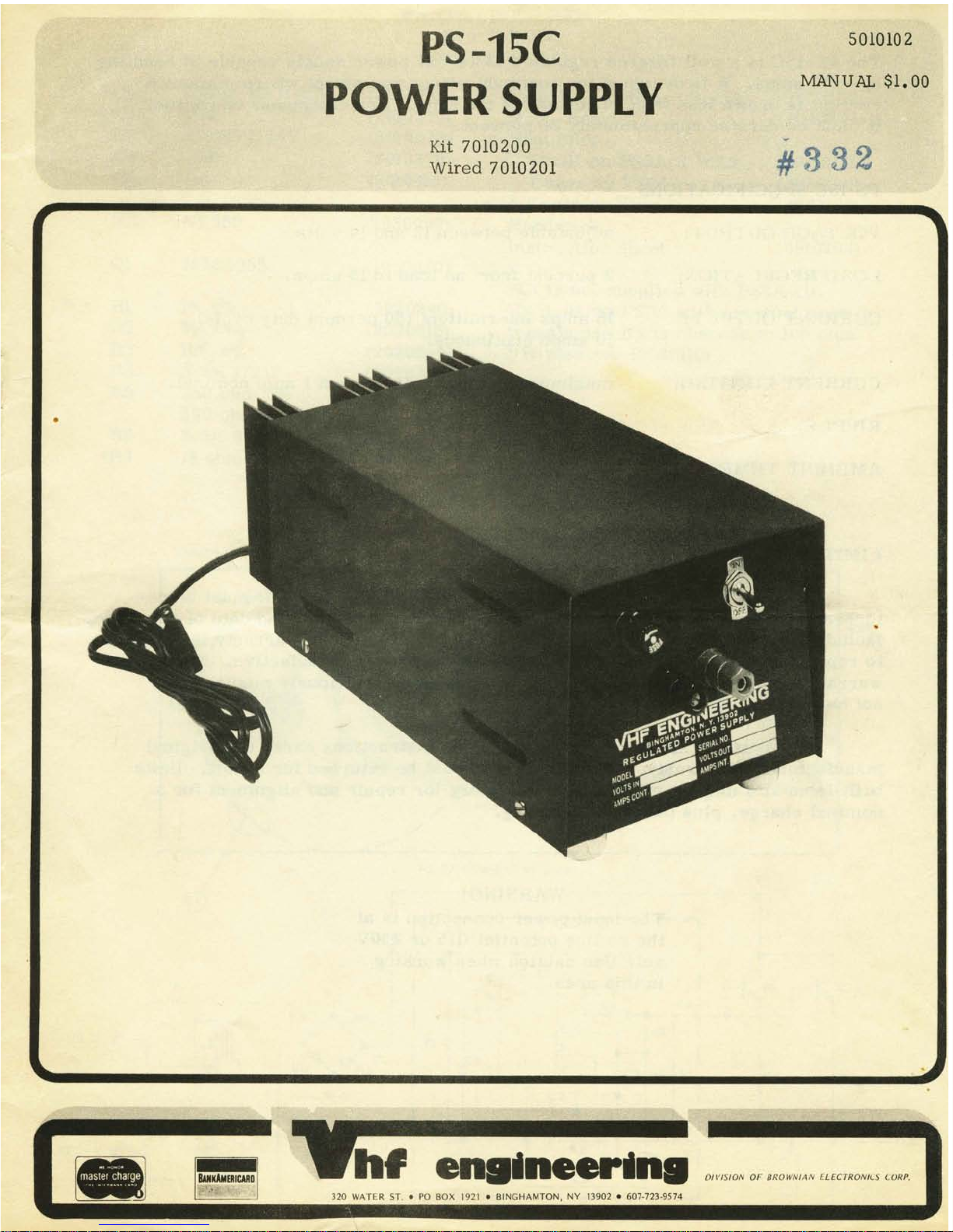
VHF Engineering PS-15C Instruction Manual
170
WATkR
ZT
PO
ROX
1971 . RINGHAMTON
NY
11902
607-721-9574

The PS-15C
is
a well filtered regulated 12-14 volt power supply capable of handlin
up to 15 amps.
It
is
designed for con~munications equipment where maximum
current
is
drawn less than 50 pcrcent of the time. For continuous operation,
it must be derated
approximately
20 percent.
*%@W$
PS-15C SPECIFICATIONS
@#
VOLTAGE OUTPUT:
adjustable between 12 and 14 volts.
LOAD REGULATION:
2
percent from no load to 15 anips.
CURRENT OUTPU'I
15 amps intermittent (50 percent duty cycle)
10 amps continuous.
CURRENT LIMITING: maximum short circuit current
1
amp nominal.
RIPPLE
:
50 MV at 10 amps.
AMBIENT TEMP:
OC
maximum.
LIMITED WARRANTY
Factory wired units are warranted for one year. The unit must be re-
turned to the factory postpaid with a note describing difficulty
and
date of purchase,
include a check to cover return postage.
Our liability under warranty
is
limited
to repair, adjustment or replacement of units proven to be defective. No further
warranty
is
expressed or implied. Units modified or obviously misused will
not be covered by the warranty.
The parts in kits built according to our instructions carry the original
manufacturers1 warranty. Defective parts must
be
returned for credit. Units
built from kits may be returned to the factory for repair and alignment for a
nominal charge, plus parts and shipping.
WARNING!
The input power connection
is
at
the ac line potential (115 or
230V
ac). Use caution when working
in this area.
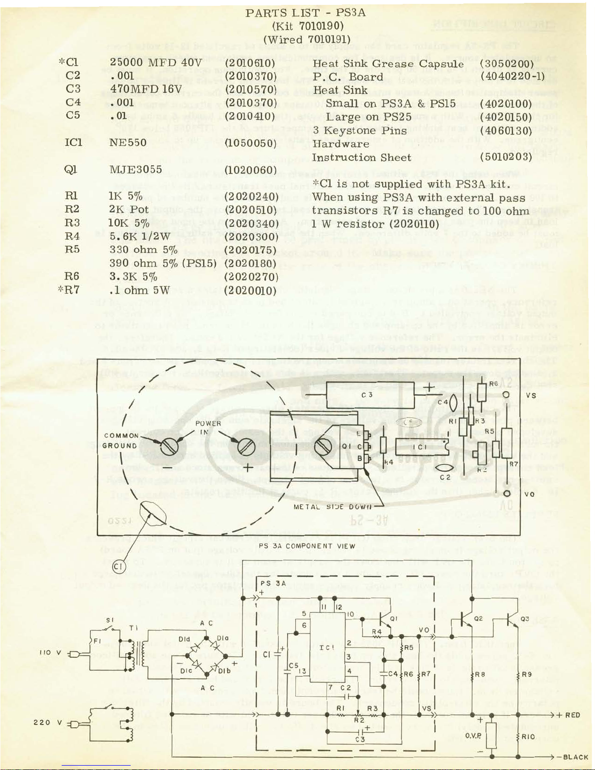
PARTS LIST - PS3A
(Kit 7010190)
(Wired 7010191)
25000
MFD
40V (2010610)
.OO1
(2 010 3 70)
470MFD 16V (2 010 5 70)
.001 (2 010 3 70)
.01 (2010410)
1K 5% (2 020240)
2K Pot (202 0510)
1OK 570 (2020340)
5.6K 1/2W (2020300)
330 ohm
570 (2020175)
390 ohm
5% (PS15) (2020180)
3.3K 570 (2 02 02 70)
.1
ohm 5W (2020010)
Heat Sink Grease Capsule
(
3050200)"
P.C. Board (4040220-1)
Heat Sink
Small on
PS3A & PS15
(4020100)
Large on PS25 (4020150)
3 Keystone Pins (4060130)
Hardware
Instruction Sheet (5010203)
*C1
is
not supplied with PS3A kit.
When using
PS3A with external pass
transistors R7
is
changed to 100 ohm
1
W resistor (2020110)
.
CIRCUIT
l,3t'SCNIF"I
ION
The PS-3A regulator card can supply up to 6 amps of regulated 12-14 volts from
an unregulated source. It
is
designed for communicptions equipment where maximum
current
is
drawn less than 50 percent of the time. For continuous operation, it must be
derated to 3 amps with the heat sink supplied. The maximum current
is
limited by the
power dissipation (input voltage minus output times current) and the current capabilities
of the pass transistor, which
is
90 watts and 10 amps respectively at room temperature
for the
TIP3055. With a supply voltage of 20 volts, the PS3A
will
handle 6 amps by
adding additional heat sinking to keep the case temperature of the TIP3055 below
120°
centigrade. With the addition of external pas€ transistors, currents up to amps can be
k
regulated.
When using the
PS3A without external pass transistors, the maximum short
circuit current
is
6
amps. When used with external pass transistors,
R-7
is
changed
to 100 ohms. The maximum 'current of 6 amps
is
multiplied
by
the number of pass
transistors. The unregulated input must be at least two volts above the output under
load to keep the pass transistors out of saturation. Any ripple on the input voltage
must be added to the 2 volts difference.
When the pass transistor saturates regulation
is
lost.
THEORY
OF
OPER.4TJON
The IVE550
is
a precision voltage regulator chip that contains a zener voltage
reference, operational amplifier, current limiter, and pass transistor.
-4 portion of the
output voltage controlled by R-4
is
compared to a reference voltage, any difference or
error
is
amplified by the op-amp and changes the bias on the internal pass transistor to
eliminate the error.
The reference voltage for the
NE550
is
1.6 volts.
Therefore, the
t
autput voltage is the ratio of the voltage divider (consisting of R-1, 2, and 3) times
1.
6.
The current limiter transistor saturates when a voltage of .6
is
applied between pins 2 and
3, shuting down the output. Therefore, with a
.1
ohm resistor for R-5, the supply will
;hut $own
when.
a-~urrent
Qf
6
amps
is
reached.
The current limiting section of
IC1 operates when a vol
between pins 2 and 3 of IC1.
This voltage
is
the algebraic sum of
developed across R-5 and
R-7.
Reverse voltage
is
the result of
r
through R-5 and R-6 to ground.
Its value
is
dependent mainly
and
the value of
R-6.
Forward voltage (disabling voltage)
is
applied across
R-7
by the
load current through the paralled
E-B
junctions of the pass transistors and
.1
ohm
emitter resistors.
Its value
is
a function of load current. When the voltage across
R-7
s
.6
volts higher than the voltage across R-5, current limiting results.
3UPPLIES USING OVP
The over-voltage protection
(OliP)
is essentially a crowbar circuit which prevents
the output voltage from
rjsing above 14 volts.
if
t!le
supply voltage (pot on PS3A board)
is
set too high, the OVP will shut down the supply as soon as it
is
turned on.
To reset
the OVP:
turn the power off - wait about one minute for the filter capacitor to discharge
-
turn the regulator pot down - reapply power - adjust the regulator pot for the desired output
volt age.
Install
IC first.
The
T1P
3055 transis!or
is
installed with the metal side down.
The
6-32
screw holds the heat sink on top
of
the transistor.
Be sure to use some silicon
grease \)ctween
the
)]cat sink and
the
trar~slfor.
The mctal part of
the
transistor
is
interndly connected to
t11e
collector.
Therefore, the screw and heat sink have full
voltage on them.
Care should be taken to prevent them from grounding out.
Observe
pclarity on the electrolytic condensers.
The board
is
usually mounted by the filter con
dcnser.
If
it'is used without the filter condenser (when used with an existing filtered
unregulated supply) it may be
]mounted on stand offs by drilling mounting holes
in
the
corners of the board,
 Loading...