

Vextrec GMB-P6EIMG User Manual

P6EIMG
High Performance
Pentium II PCI
Mainboard
User’s Guide
Version 1.02

WARNING
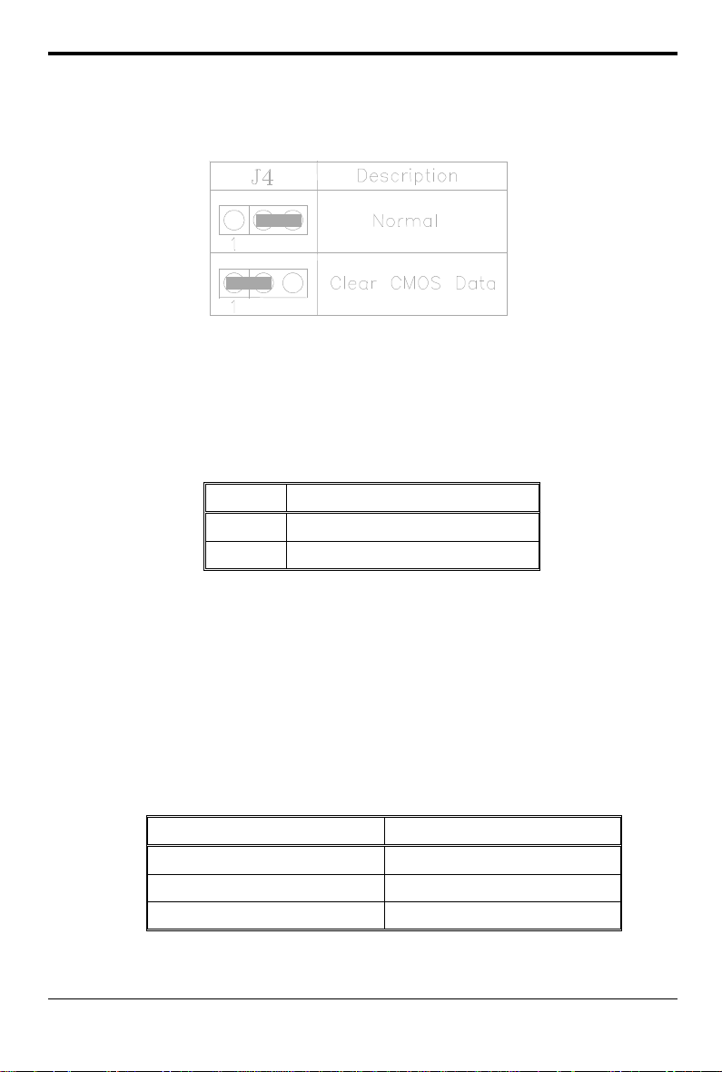
For the system to operate normally, please make sure J4 of the mainboard is set as below. Refer
to Fig. 4 in this manual for the location J4.
If J4 is shorted to 1-2, no CMOS data can be retained.
CAUTION
The motherboard is an electrostatic sensitive device. Don’t open or handle except at a staticfree workstation.
POWER OFF
It needs to hold the power switch 4 seconds to turn off the power.
Windows, MS-DOS, and MS Word are trademarks of Microsoft Corporation.
Novell, Netware are trademarks of Novell, Inc.
Lotus, 1-2-3, and Symphony are trademarks of Lotus Development Corporation.
PC, AT, PC-DOS, OS/2 and Presentation Manager are trademarks of IBM Corporation.
UNIX is the trademark of AT&T.
Intel i82440EX and Pentium II are registered trademark of Intel Corporation.
All other brand and product names are trademarks or registered trademarks of their respective
companies.
The information presented in this publication has been carefully checked for reliability; however,
no responsibility is assumed for inaccuracies, whereas, specification is subjected to change
without notice.
2

CONTENTS
CHAPTER 1 INTRODUCTION 5
CHAPTER 2 JUMPER SETTINGS 7
2.1 JUMPERS PRESENTATION 7
2.2 GRAPHICAL DESCRIPTION OF JUMPER SETTINGS 8
2.3 CPU SPEED 9
2.4 J4 - CLEAR CMOS DATA 10
2.5 J24 – POWER ON/OFF AFTER POWER FAILURE 10
2.6 MEMORY CONFIGUARTION 10
CHAPTER 3 CONNECTOR CONFIGURATION 11
3.1 J1 - SPEAKER 12
3.2 J2 - POWER ON/OFF SWITCH 12
3.3 J3 - RESET 12
3.4 J5 – KEYLOCK CONNECTOR 12
3.5 J6 - HDD LED 13
3.6 J7 - IrDA CONNECTOR 13
3.7 J9, J10 – PRIMARY/SECONDARY IDE CONNECTORS 13
3.8 J11 – CD-ROM AUDIO CONNECTOR (SONY) 13
3.9 J15 – CD-ROM AUDIO CONNECTOR (MITSUMI/PANASONIC) 14
3.10 J16, JA1 – CPU, SYSTEM/POWER SUPPLY FAN CONNECTOR 14
3.11 J19 - FLOPPY DRIVE CONTROLLER 14
3.12 JP5 – WAKE UP ON LAN 14
3.13 SLOT 1 FOR PENTIUM II CPU 14
3.14 PS1 - ATX POWER SUPPLY CONNECTOR 15
3.15 PS/2 KEYBOARD CONNECTOR 15
3.16 PS/2 MOUSE CONNECTOR 15
3.17 UNIVERSAL SERIAL BUS PORT 0 & 1 15
3.18 SERIAL PORT COM1 & COM2 16
3.19 PARALLEL PORT CONNECTOR 16
3.20 AUDIO PORT CONNECTOR 16
3.21 RETENTION MECHANISM KITS INSTALLATION GUIDE 16
CHAPTER 4 AWARD BIOS SETUP GUIDE 21
4.1 AWARD BIOS SETUP 21
4.2 STANDARD CMOS SETUP 23
4.3 BIOS FEATURES SETUP 24
4.4 CHIPSET FEATURES SETUP 26
4.5 POWER MANAGEMENT SETUP MENU 28
4.6 PCI CONFIGURATION 30
4.7 INTEGRATED PERIPHERALS SETUP MENU 32
4.8 LOAD SETUP DEFAULTS MENU 34
4.9 SUPERVISOR PASSWORD 34
3

4.10 USER PASSWORD 34
4.11 IDE HDD AUTO DETECTION 35
4.12 SCSI HARD DISK INSTALLATION 35
4.13 SAVE & EXIT SETUP MENU 35
4.14 EXIT WITHOUT SAVING MENU 35
CHAPTER 5 SOFTWARE INSTALLATION 36
5.1 INTEL 82440EX PCI AGP CHIPSET PATCH UTILITY FOR
WINDOWS 95 36
5.2 INTEL BUS MASTER IDE DRIVER FOR WIN 95 INSTALLATION 36
5.3 SOUND DRIVER INSTALLATION 37
5.4 THE AUDIORACK32 FOR WIN95 37
5.4.1 INTRODUCTION 38
5.4.2 INSTALLING THE AudioRack32 38
5.4.3 UNINSTALLING THE AudioRack32 41
CHAPTER 6 FLASH AND DMI UTILITY 42
6.1 AWARD FLASH UTILITY 42
6.2 DESKTOP MANAGEMENT INTERFACE (DMI) OVERVIEW 44
APPENDIX A QUICK GUIDE 48
4

CHAPTER 1 INTRODUCTION
Preface
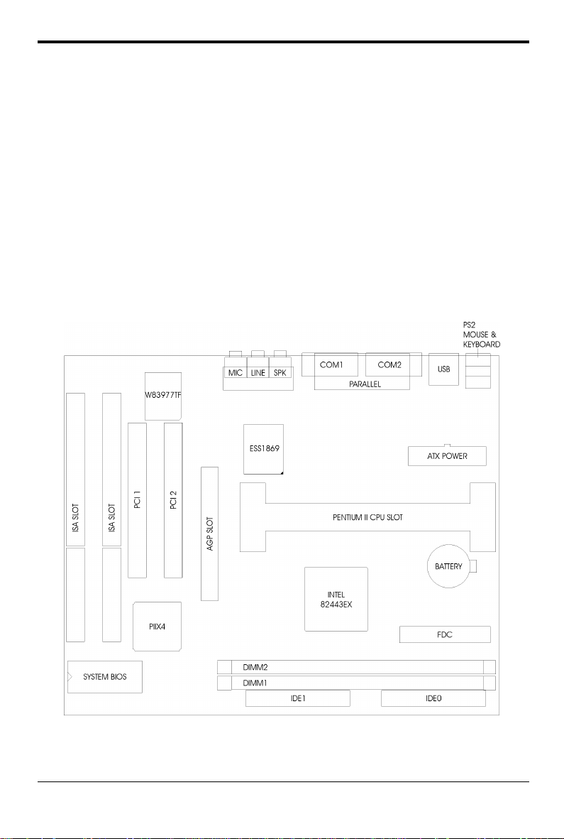
The motherboard is a 4 layer, Mini ATX form factor high performance PCI/AGP mainboard.
It includes Intel i82440EX system chipset, Winbond W83977TF Super I/O controller, ESS
1869 Sound Chip.
Features
Processor
• Intel Pentium II series.
• The mainboard can run with following speeds:
233, 266, 300 and 333MHz
Chipset
• Intel i82443EX (PCI A.G.P. Controller)
• Intel 82371AB (PCI ISA IDE Xcelerator)
• Winbond W83977TF (Super I/O Controller)
• ESS 1869 (Audio Drive Sound Controller)
Main Memory
• Memory configurations up to 256MB SDRAM or 512MB EDO.
• DIMM socket for SDRAM (3.3V unbuffered).
• Support both Synchronous DRAM and Extended Data Output (EDO) Mode DRAM
Modules.
• ECC Function ensure data correction and integrity.
Multi I/O
• On board Multi-I/O supports two serial, one parallel ports and floppy drive controller.
• Serial ports are 16550 Fast UART compatible.
• Parallel port has EPP and ECP capabilities.
• PS/2 keyboard and PS/2 mouse connector is provided.
• IrDA supported.
• USB supported.
Accelerated Graphics Port (AGP) Interface
• A.G.P. specification compliant
• A.G.P. 66/133MHz devices supported
PCI IDE
• On board supports PCI Master IDE Controller, two connectors support up to four IDE
devices such as HDD, CD ROM drive and Tape Back-up drives, etc.
• PCI Master IDE controller supports PIO Mode 3 and 4 devices, I/O data transfer rate can be
up to 16.6MB/s.
• Ultra DMA Mode supported. Transfer rate can be up to 33MB/s.
5
Chapter 1
Sound Controller (Optional)
• Compatible with all major PC sound standards, including Sound Blaster Pro, MPU-401
and Windows Sound System.
• Plug-and-Play support for Audio, Joystick, FM Controller, MPU-401.
• Wave Audio support sample rates from 4KHz to 44KHz.
• Full-duplex monophonic mode, half-duplex stereo mode.
System BIOS
• Award BIOS (128KB Flash EPROM).
Slots
• One AGP slot
• Two PCI slots
• Two ISA slots
Form Factor
• Mini ATX Form Factor Size (244mm x 200mm) 4 Layer
Fig. 1 Key Components of the Mainboard
6
CHAPTER 2 JUMPER SETTINGS
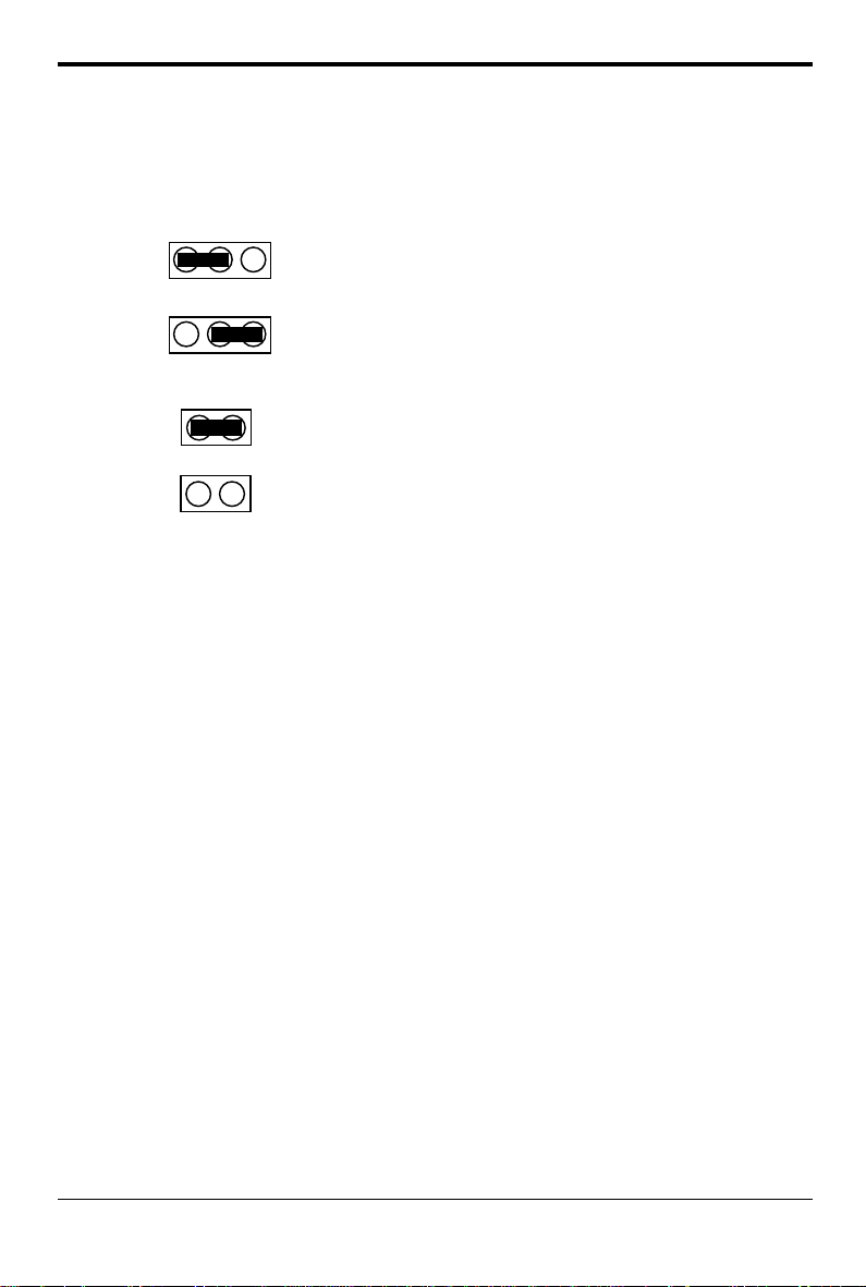
2.1 JUMPERS PRESENTATION
Pins 1 and 2 are shorted with a jumper cap.
1 2 3
Pins 2 and 3 are shorted with a jumper cap.
1 2 3
The jumper is shorted when the jumper cap is placed
over the two pins of the jumper.
The jumper is open when the jumper cap is removed
from jumper.
Jumpers Convention
Different color of jumper caps (mini-jumpers) are used on the board to represent
different usage of the jumpers:
Red: CPU Clock setting
Black: Other
7
Chapter 2
2.2 GRAPHICAL DESCRIPTION OF JUMPER
SETTINGS
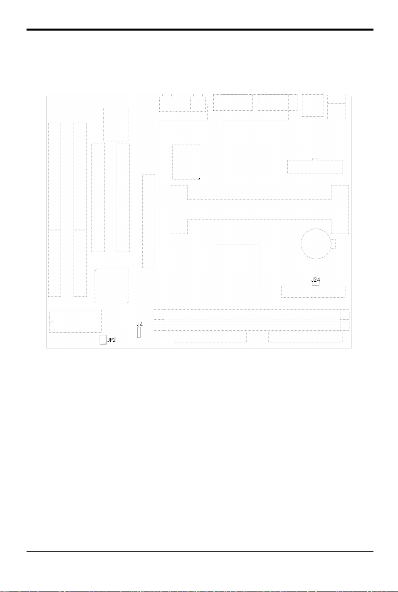
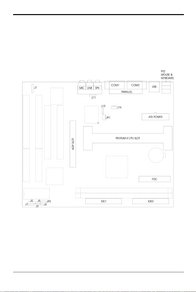
Fig. 2 Jumper Location of the mainboard
8
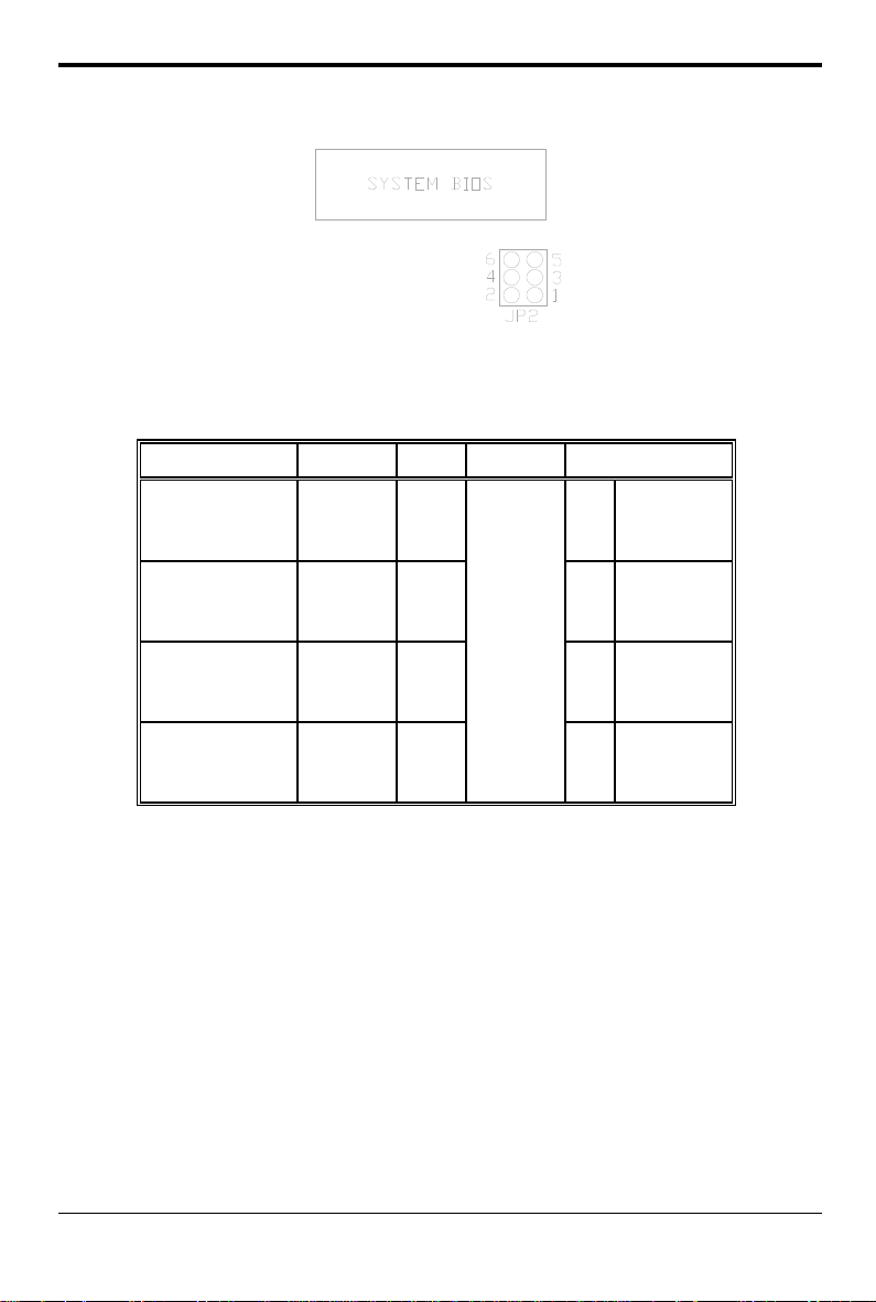
2.3 CPU SPEED
The table below summaries the CPU frequence and settings of each jumper of the
motherboard.
CPU Type Freq. Ratio Bus Freq. Rating Setting
Pentium II 233MHz 3.5x JP2: 1-2 OFF
Pentium II 266MHz 4.0x
Pentium II 300MHz 4.5x JP2: 1-2 OFF
Pentium II 333MHz 5.0x JP2: 1-2 ON
Fig. 3
66MHz
Jumper Settings
3-4 OFF
5-6 ON
JP2: 1-2 ON
3-4 ON
5-6 OFF
3-4 ON
5-6 OFF
3-4 OFF
5-6 OFF
Table 1: Jumper Setting
9
Chapter 2
2.4 J4 - CLEAR CMOS DATA
J4 is used to clear the content of the CMOS Data in the RTC (build in PIIX4 chip).
Table 2: Clear CMOS Data
2.5 J24 – POWER ON/OFF AFTER POWER FAILURE
This jumper sets the power of the system after the main power has failed then
recovered.
J24 System After Power Failure
ON ON
OFF OFF
Table 3
2.6 MEMORY CONFIGUARTION
The mainboard lets user upgrade system memory via DIMM sockets on the
mainboard. On board memory is located in four banks: Bank 0 - 3. Two DIMM
sockets are provided for EDO DRAM or Synchronous DRAM. Table 4 provide the
typical memory configurations supported by the mainboard.
The maximum memory size is up to 256MB (SDRAM) or 512MB (EDO). The size
of each DIMM can be 8MB, 16MB, 32MB, 64MB or 128MB.
Bank 0/1 (DIMM2) Bank 2/3 (DIMM1)
Installed None
None Installed
Installed Installed
Table 4
10
CHAPTER 3 CONNECTOR
CONFIGURATION
Once the mainboard has been fastened into system case, the next step is to connect the internal
cables. The internal cables are wire leads with plastic female connectors that attach to the
connectors. The mainboard connectors have varying numbers of pins and are the points of
contact between the mainboard and other parts of the computer.
Fig 4 Connector Location
11
Chapter 3
3.1 J1 - SPEAKER
J1 is a four pins connector, which is used to connect the system speaker.
Fig. 5 Speaker
3.2 J2 - POWER ON/OFF SWITCH
It is used to switch on or off the ATX power supply. The power is turned on by
short the power switch once. It needs to hold the power switch about 4 seconds to
turn it off when it has not start to display.
3.3 J3 - RESET
Attach the Reset switch cable to this connector. The Reset switch restarts the
system.
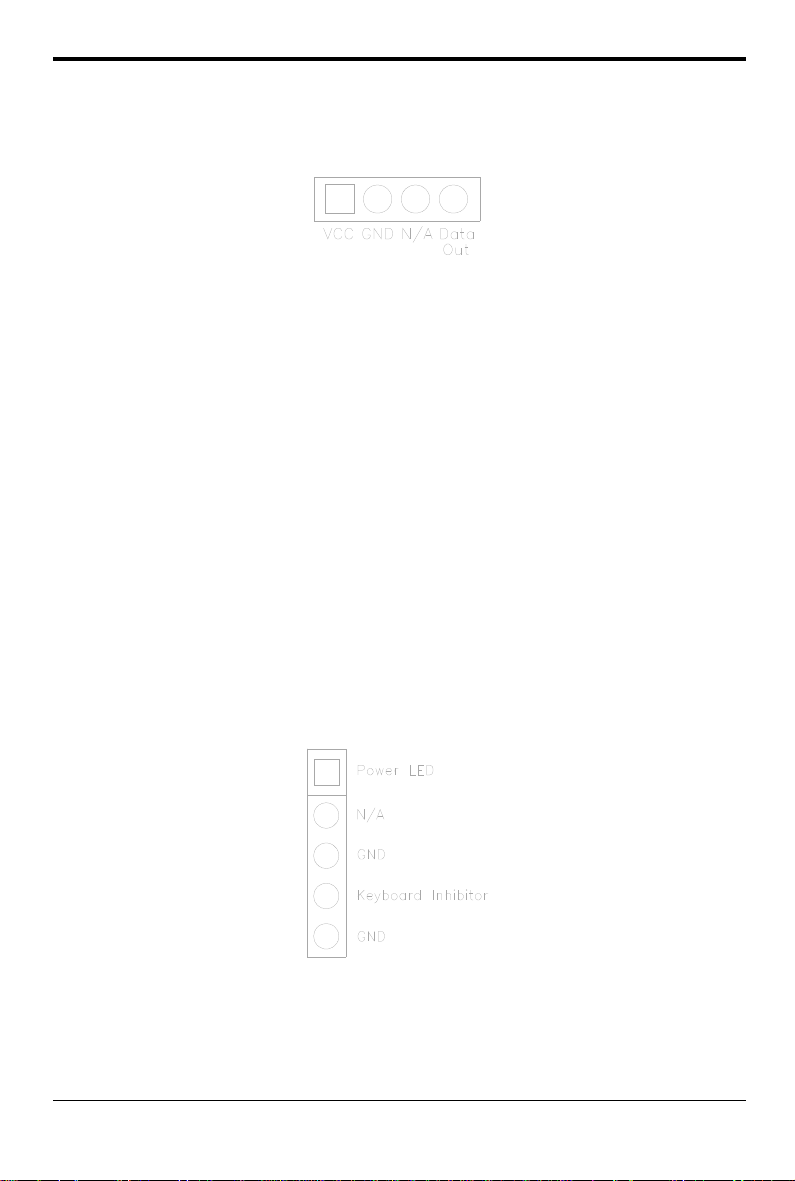
3.4 J5 – KEYLOCK CONNECTOR
Attach the power led cable to this connector. If the system is power on, the indicator
lights.
Fig. 6 Keylock Connector
12
3.5 J6 - HDD LED
J6 is usually connected to a HDD LED on front of the system case. If the HDD is in
operation, the indicator lights during operation.
Fig. 7 HDD LED
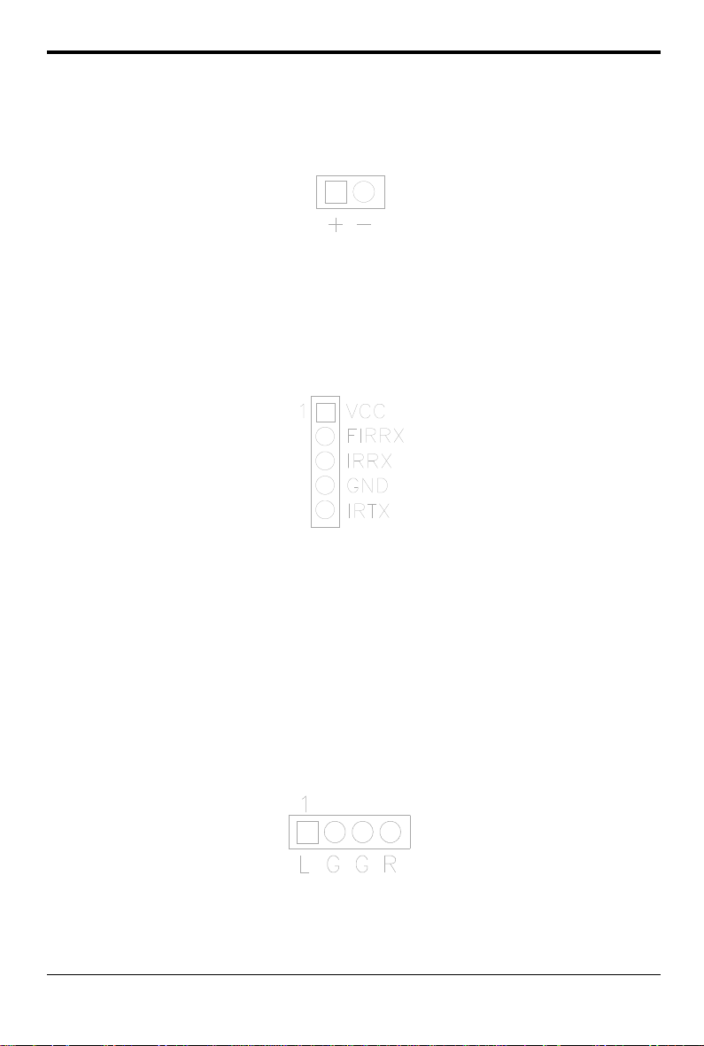
3.6 J7 - IrDA CONNECTOR
J7 is a IrDA connector that use UART2 as interface of IrDA Infrared and ASKIR.
Fig. 8 IrDA Connector
Connector Configuration
3.7 J9, J10 – PRIMARY/SECONDARY IDE
CONNECTORS
These connectors support the provided IDE hard disk ribbon cable. After
connecting the single end to the board, connect the two plugs on the other end to
your hard disk or other device.
3.8 J11 – CD-ROM AUDIO CONNECTOR (SONY)
Fig. 9 CD-ROM Audio
13
Chapter 3
3.9 J15 – CD-ROM AUDIO CONNECTOR
(MITSUMI/PANASONIC)
Fig. 10 CD-ROM Audio
3.10 J16, JA1 – CPU, SYSTEM/POWER SUPPLY FAN
CONNECTOR
J16 is a three-pin connector, which is used to connect with the CPU Fan Power
cable. JA1 is another three-pin connector for optional System/Power Supply Fan.
3.11 J19 - FLOPPY DRIVE CONTROLLER
This connector supports the floppy drive ribbon cable. After connecting the single
end to the board, connect the two plugs on the other end to the floppy drive.
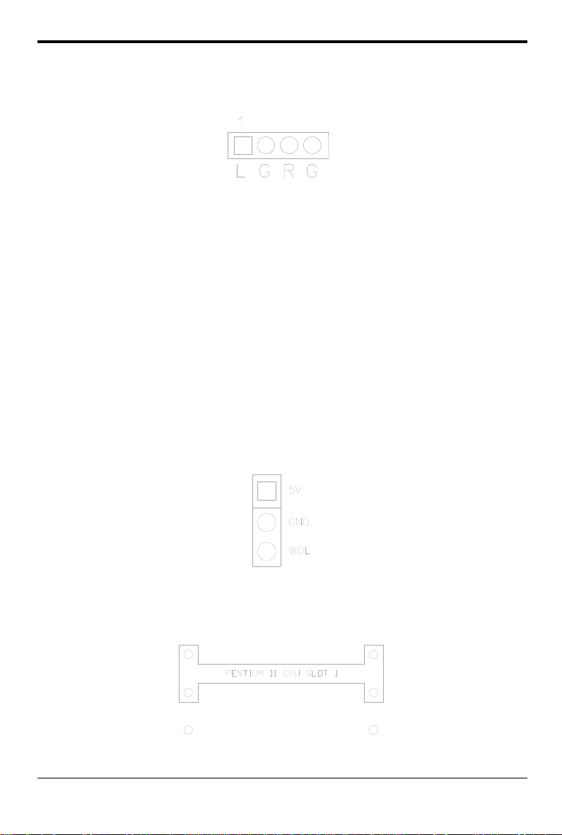
3.12 JP5 – WAKE UP ON LAN
Fig. 11 Wake up On LAN
3.13 SLOT 1 FOR PENTIUM II CPU
Fig. 12 Slot 1 for Pentium CPU
14
Connector Configuration
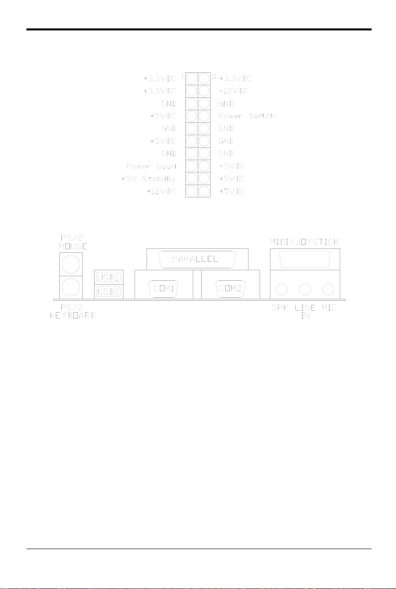
3.14 PS1 - ATX POWER SUPPLY CONNECTOR
Fig. 13 ATX Power Supply Connector
Fig. 14 I/O Connector
3.15 PS/2 KEYBOARD CONNECTOR
This connector is a six-pin female mini DIN connector using a PS/2 plug. If a
standard AT size keyboard plugs, you may use the DIN to mini DIN adaptor.
3.16 PS/2 MOUSE CONNECTOR
This connector is a six-pin female mini DIN connector using a PS/2 plug. Plug the
jack on the PS/2 keyboard cable into this connector.
3.17 UNIVERSAL SERIAL BUS PORT 0 & 1
These connectors are two four pin female sockets which are available for connecting
USB device.
15
 Loading...