

Vextrec GMB-486SG User Manual

GMB-486SG
High Performance
486
VLB Motherboard
User’s Manual
For
GMB-486sg v2
Manual Edition 6.03

This guide contains instructions for configuring and installing the mainboard.
• Chapter 1,
• Chapter 2,
mainboard's jumpers. Brief sections on installing memory.
• Chapter 3,
• Chapter 4,
• Chapter 5,
• Chapter 6,
Introduction
Hardware Configuration
Mainboard Installation
BIOS Setup
BIOS POST Messages
BIOS Default Drive Table
, acquaints user with th e special f eatu res of th e mainboard.
, gives information on configuring memory and setting the
, is an overview of how to install the mainboard in a system .
, provides the BIOS information for system configuration.
, provides references for all POST error mes s ag es .
, provides a Default Drive Disk table contained in Setup.
WARNING
For the system to operate normally please make sure JP16 of the mainboard is set as below. Refer to Fig 2 in
this manual for the location JP16.
If JP16 is open, no
CMOS data can be
retained.
The information presented in this publication has been carefully checked for reliability; however, no
responsibility is assumed for inaccu racies, whereas, specification is subjected to change with ou t n otice.
All rights reserved. No part of this Manual may be reproduced in any form without the written permission.
i

UNPACKING THE MAINBOARD
The Mainboard comes packed in a s t u rdy cardboard shipping carton. The carton con tai n s :
• The Mainboard
• This User's Guide
Note: Do not remove the mainboard from its original packing until ready to install.
The mainboard is easily damaged by static electricity. Observe the following precautions while unpacking and
installing the mainboard.
1. Touch an unpainted area of the system chassis before handling the mainboard or any component.
Doing so, discharges the static ch arg e th e u ser's body may h ave bu ilt.
2. Remove the mainboard from its anti-static wrapping and place it on a grounded surface, component
side up.
3. Inspect the mainboard for damage. Shipping may have loosened integrated circuits from their
sockets. If any integ rated circuit appears loos e, press caref u lly to seat it firmly in th is s ocket.
Do not apply power if the mainboard appears damaged. If there is damage to the board, or items are missing,
contact dealer immediately .
ii

CONTENTS
CHAPTER 1 INTRODUCTION 1
1.1 KEY FEATURES 1
1.2 MAINBOARD COMPONENTS 3
1.3 VES A LOCAL BUS SPECIAL FEATURES 4
CHAPTER 2 HARDWARE CONFIGURATION 5
2.1 JUMPER AND MEMORY BANK LOCATIONS 5
2.2 JP8, JP10-JP15, JP21, JP22, JP24, JP25, JP30,
JP31, JP34-JP36, JP38 - CPU TYPE CONFIGURATION 6
2.3 CPU INSTALLATION 14
2.4 CACHE CONFIGURATION 15
2.4.1 UPGRADING CACHE 15
2.4.2 CACHE SIZE AND MEMORY LOCATIONS 16
2.4.3 CACHE CHIP SOCKETS AND JUMPER LOCATIONS16
2.4.4 JP1-JP4, JP33 - CACHE & TAG RAM JUMPER SETTING 17
2.4.5 INSTALLING CACHE CHIPS 18
2.5 JP28, JP29 - VL-BUS IDENTIFY PINS 19
2.6 JP16 - CMOS RAM BATTERY SETTING 19
2.7 JP17 - MONITOR SETTING 20
2.8 JP20 - CPU CLOCK DELAY 20
2.9 JP5, JP6, JP7 - CPU FREQUENCY
CONFIGURATION 21
2.10 JP37 - FLASH ROM JUMPER 21
2.11 MEMORY INSTALLATION 22
2.11.1 INSTALLING SIMM 25
CHAPTER 3 MAINBOARD INSTALLATION 27
3.1 COMPONENTS 27
3.2 INSTALLING THE MAINBOARD 28
3.3 CONNECTION THE MAINBOARD 28
3.3.1 CONNECTION LOCATIONS 29
3.4 CONNECTORS 29
3.4.1 CN1 - KEYBOARD CONNECTOR 29
3.4.2 CN2 - POWER SUPPLY CONNECTOR 30
3.4.3 J1 - EXTERNAL BATTERY 30
3.4.4 J2 - GREEN POWER SUPPLY CONNECTOR 31
3.4.5 J3 - TURBO SWITCH CONNECTOR 31
3.4.6 J4 - TURBO LED CONNECTOR 32
3.4.7 J5 - SPEAKER CONNECTOR 32
3.4.8 J6 - RESET SWITCH CONNECTOR 32
3.4.9 J7 - KEYLOCK & POWER LED CONNECTOR 33
3.4.10 JP26 - GREEN PC BREAK SWITCH 33
3.4.11 JP27 - SM_LED CONNECTOR 33
3.5 SYSTEM ASSEMBLY OVERVIEW 34
CHAPTER 4 AWARD BIOS SETUP 35
4.1 ENTERING SETUP 35
4.2 CONTROL KEYS 36
4.3 GETTING HELP 36
4.4 THE MAIN MENU 37
4.4.1 STANDARD CMOS SETUP MENU 38
iii

4.4.2 BIOS FEATURES SETUP MENU 39
4.4.3 CHIPSET FEATURES SETUP MENU 40
4.4.4 POWER MANAGEMENT SETUP MENU 41
4.4.5 LOAD BIOS DEFAULTS MENU 43
4.4.6 LOAD SETUP DEFAULTS MENU 43
4.4.7 PASSWORD SETTING MENU 43
4.4.8 IDE HDD AUTO DETECTION MENU 44
4.4.9 SAVE & EXIT SETUP MENU 44
4.4.10 EXIT WITHOUT SAVING MENU 44
CHAPTER 5 BIOS POST MESSAGE 45
5.1 POST BEEP 45
5.2 ERROR MESSAGES 45
iv

Introduction
CHAPTER 1 INTRODUCTION
The mainboard is a 2/3 body AT size high-performance mainboard that provides with basic elements on which
to build an advanced computer. The mainboard running from 25MHz to 133MHz, supports Normal 486
CPUs, Intel's SL-Enhanced 486, Cyrix Cx486S/DX/DX2, UMC U5SX-486, P24D/P24T; and optionally
support P24C(486DX4), Am486DX2/DX4(3.45V), Enhanced Am486DX2/DX4 (3.45V), Cx486DX2V66/V80, Cyrix DX4-100, Cx5x86-100, TI DX2-80, IBM486-4V3100GC/GIC and AMD-X5-133ADW
CPUs.
1.1 KEY FEATURES
The advanced features of the m ain board in clu de:
• Supports Intel ' s S L En hanced 80486DX2/DX/SX,
Cyrix's C x 486S/ DX/DX2, UMC U5S X-486, normal 486, P24D/P24T;
and optionally s u pport P24C(486DX4), Am486DX2/DX4(3.45V),
Enhanced Am 486DX2/DX4 (3.45V), C x 486DX2-V66/V80, Cyrix
DX4-100, Cx5x86-100, TI DX2-80, IBM 486-4V3100GC / GIC an d
AMD-X5-133ADW CPUs.
• Supports Cache Wri te back C PU (P24T/P24D/Cx486S /DX/ DX2/DX2V),
and Enhanced Am486DX2/DX4, Cyrix DX4/5x86, IBM 486 an d
AMD-X5 CPUs.
• 100% IBM PC-AT compatible, single chi ps 486 s olution.
• Provides power saving features to allow a system, through the control of
BIOS, to reduce the CPU clock frequency down to 0MHz
(STOP CLOCK) when the system is idle.
• Supports Pow er Management Mode
- Supports the SMM and t h e SMI
- CPU Stop Clock Fun c ti on
- Long and Sh ort S ystem Timers
- Supports the A PM cont rol
- Supports Break Switch control
- Power Saving also on non-SMI CPU
- More System Ev en t Monitorin g an d th e Pow er s av in g C ont rol
• Direct Mapped Cache Controller
- Write-Back or Write-Through Schemes
- Bank Interleave or Non-Interleav e C ach e
- Flexible Cache S ize: 128/256/ 512KB
• Memory s ize from 1MB to 128MB, possible usi n g combinations of
1M, 2M, 4M, 8M, 16M, 32M, or 64M 72-pin SIMM modul es i n
four memory banks.
• Easy upgrade th e system, just chang e C PU, or and alter jumper only.
• System & v ideo Bios Sh adow, optional caching of sh adowed system &
video BIOS.
1

Chapter 1
• Hidden DRAM refres h su pport .
• Support KB control Turbo/Det u rbo mode select.
• Support 7 Direct Memory Access channels and 16 Interru pt lev els .
• Three 16-bit I/O slots , on e 8- bi t I/ O s lot s , an d t h ree St an dard VES A
Local Bus master slot.
• Battery backup for CMOS conf ig u ration an d real time clock/calendar.
• 8MHz AT Bus clock & speed chan g eable by hardware or keyboard, C PU
clock adjustable by jumper.
• 2/3 Baby AT board size = 220mm(W) X 250mm (L ).
2
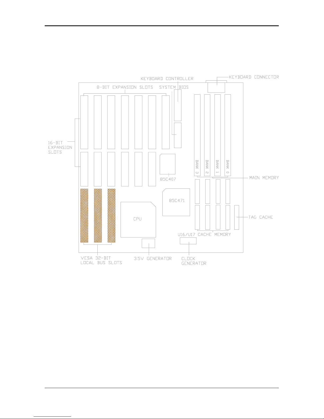
1.2 MAINBOARD COMPONENTS
This section gives a brief description of key components on the mainboard. Refer to Fig 1 for
component locations.
Introduction
Fig 1 Key Components of th e Mainboard
3

Chapter 1
1.3 VESA LOCAL BUS SPECIAL FEATURES
• Three-bus master are supported on the VESA Local-Bus. The VESA Local-Bus connector type is a
standard 32-bit Micro Channel type connector, and is located inline with a s ystem I/O bus connector.
• Three slots are provided on the mainboard. Either with one master or three master slots.
• The VESA Local-Bus can support high speed video controllers, and other peripherals, such as hard
disk controllers, LAN adapters , an d s o on.
• Interface protocol depends on the CPU speed, but protocol selection and switching is invisible to all
add-in boards, software, and end users. The VESA Local-Bus always remains totally transparent to
all application software.
• 32-bits optimum data bus width
4
Hardware Configuration
CHAPTER 2 HARDWARE CONFIGURATION
This chapter describes how to set the mainboard jumpers for cache memory and display type, and how to
install memory modules.
Before beginning the conf ig u ration , us er s h ould tak e th e f ollowing precautions:
• Turn off the pow er s u ppl y, and unplug th e power cord before begin.
• Unplug all cables that connect the mainboard to any external devices.
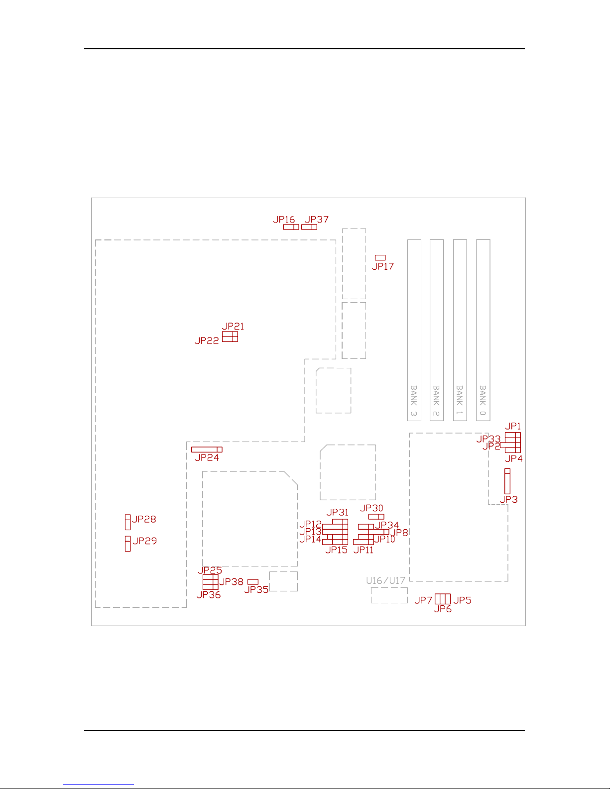
2.1 JUMPER AND MEMORY BANK LOCATIONS
Fig 2 Jumper and Memory Bank Locations
5
Chapter 2
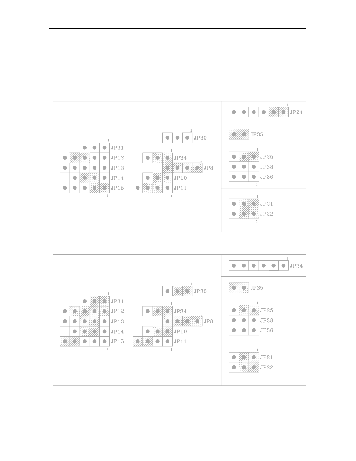
2.2 JP8, JP10-JP15, JP21, JP 22, JP 24, JP 25, JP 30,
JP31, JP34-JP36, JP38 - CPU TYPE CONFIGURATION
The mainboard can support processor at different speed. Various jumpers are required to setup for
installing different CPU. Refer to Fig 2 for the jumpers’ location, and set the jumper according to the
following table:
JP8, JP10-JP15, JP21, JP22, JP24, JP25, JP30, JP31, JP34-JP36, JP38
--CPU Type Configuration
Table 1A: CPU Type: - P24T
Table 1B: CPU Type: - P24D (DX2)
6
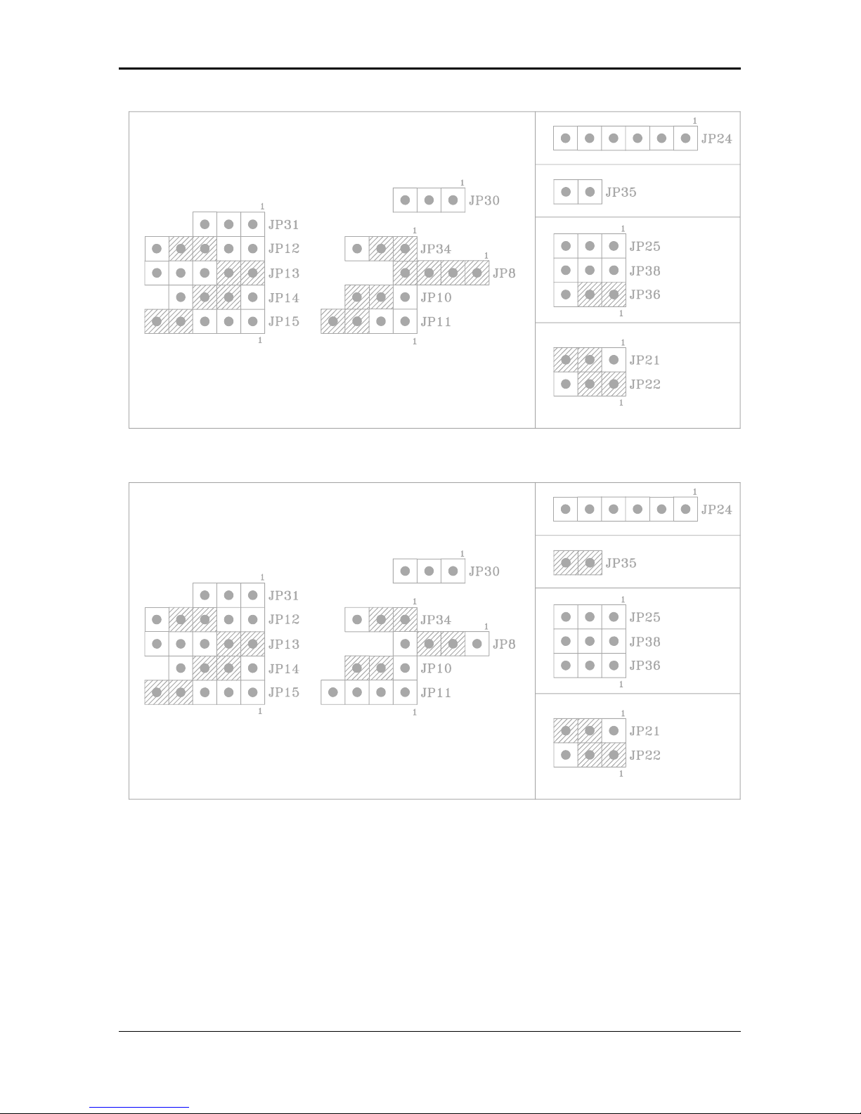
Table 1C: CPU Type: - P24C (DX4) (OPTIONAL)
Hardware Configuration
Table 1D: CPU Type: - 486SX/SLE 486S X
7
Chapter 2
Table 1E: CPU Type: - 486DX/DX2, SLE 486DX/DX2
Table 1F: CPU Type: - Cyrix 486S
8
Table 1G: CPU Type: - Cyrix 486DX/DX2
Hardware Configuration
Table 1H: CPU Type: - UMC U5SX-486
9
Chapter 2
Table 1I: CPU Type: - Enhanced Am486DX2/DX4 (3.45V)
(A80486DX2-XXSV8B/A80486DX4-1XXSV8B)
For DX4-100 CPU Frequency: 33MHz
For DX4-120 CPU Frequency: 40MHz
Table 1J: CPU Type: - Am486DX2 (3.45V) (Optional)
10
 Loading...