

Page 1

SAT 507D
SERVICE MANUAL
1999
Page 2
2
DO NOT CHANGE ANY MODULE UNLESS THE SET IS PLUGGED OFF.
SAT-507D operates between 85 with 265VAC main supply and this voltage level has
THE RISK OF ELECTRICAL SHOCK.
Safety precautions
• Servicing of this satellite receiver should only be carried out by a qualified person.
• DISCONNECT THE RECEIVER’S MAIN SUPPLY BEFORE OPENING THE COVER.
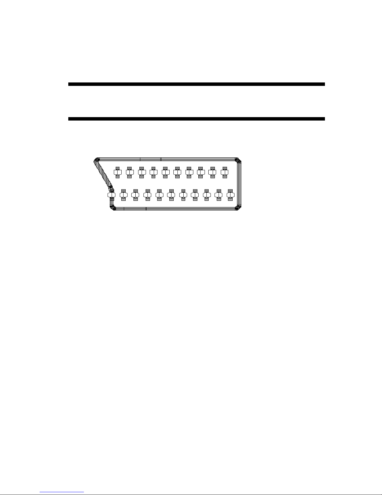
SCART CONNECTIONS
20 18 16 14 12 10 8 6 4 2
21 19 17 15 13 11 9 7 5 3 1
DECODER/VCR SCART TV SCART
1) Audio out R 1) Audio out R
2) Audio in R 2) No connection
3) Audio out L 3) Audio out L
4) Audio ground 4) Audio ground
5) No connection 5) No connection
6) Audio in L 6) No connection
7) No connection 7) No connection
8) Video Int/Ext Switch 8) Video Int/Ext switch
9) No connection 9) No connection
10) No connection 10) No connection
11) Green in 11) Ground
12) No connection 12) No connection
13) No connection 13) No connection
14) No connection 14) No connection
15) No connection 15) No connection
16) No connection 16) No connection
17) Video ground 17) Video ground
18) Ground 18) Ground
19) Video out 19) Video out
20) Video in 20) No connection
21) Ground 21) Ground
Page 3

3
1. INTRODUCTION:
SAT-507D satellite receiver is designed to work for years under proper conditions without
any maintenance and produced with quality control assurance. SAT-507D is a basic model
satellite receiver. The technical information of the receiver will be explained in the
following pages.
2. POWER SUPPLY:
The TOPSWITCH concept is used in power supply. The switching and control circuit is
associated with IC03(TOP223). R251, C201 and D10 are protection circuit of IC03. The
5V regulation is provided by using IC06 (opto-coupler), secondary side components
(C135, D09, R221, R218, R220, IC08, C78, C274) which are coming to reference side of
transformer. IC02 (op-amp) and Q56 with external components generate the LNB voltage.
After the max LNB current or LNB short circuit controls are detected by Q07 and Q08,
the LNB power is cut-off by IC07. The 5V standby switching is made by (Q02). Q12
switches 13/18V. The 22kHz signal generated from IC01 (STV0042A) and it is switched
by Q10, Q11 and after amplified by IC02 than added to LNB voltage via Q56. In order to
reduce the power consumption in standby mode, Q03V switches off the 5V power supply.
When the double LNB inputs tuner is used, the switching of LNB powers is done by Q38,
Q40, Q35, Q39, Q34, Q29, Q25.
3. VIDEO CIRCUIT:
The composite video is first set to a standard level by means of a 64 step gain controlled
amplifier( Pin 17 of IC01 is base band video input ). In the case that the modulation is
negative, an inverter can be switched in. Then energy dispersal is removed by a sync tip
clamping circuit, which is used on all inputs to a video switching matrix, thus making sure
that no DC steps occur when switching video sources. The matrix can be used to feed
video to and from decoders, VCR’s and TV’s. Additionaly all the video outputs are
tristate type (high impedance mode is supported), allowing a simple parallel connections
to the scarts. After the video processing is finished, the external video enter to pin18 of
IC05. The sync of video is generated by R121, C45, R269 , C275, C46, R123, R227,
C177 and send to pin12 of IC07. According to decision of video, the selected video
(internal/external) is sent to the video outputs( scarts, modulator etc.) at pin16 of IC05.
4. SOUND CIRCUIT:
The two audio channels are totally independent except for the possibility given to output
on both channels only one of the selected input audio channels. To allow a very cost
effective application, each channel uses PLL demodulation. Neither external complex
filter nor ceramic filters are needed. The frequency of the demodulated subcarrier is
chosen by a frequency synthesizer which sets the frequency of the internal local oscillator
by comparing its phase with the internally generated reference. When the frequency is
reached, the microprocessor switches in the PLL and the demodulation starts. At any
moment the microprocessor can read from the device (watchdog registers) the actual
frequency to which the PLL is locked. It can also verify that a carrier is present at the
wanted frequency (by reading AMPLK status bit) thanks to a synchronous amplitude
detector, which is also used for the audio input AGC. In order to maintain constant
amplitude of the recovered audio regardless of variations between satellites or subcarriers,
the PLL loop gain may be programmed from 56 values. Any frequency deviation can be
accomodated (from ±30kHz till ±400kHz). In the typical application, the
Page 4

4
STV0042Aoffers two audio de-emphasis 75ms and 50ms. Adynamic noise reduction
system (ANRS) is integrated into the STV0042A using a low pass filter, the cut-off
frequency of which is controlled by the amplitude of the audio after insertion of a bandpass filter. Two types of audio outputs are provided : one is a fixed 1VRMS and the other
is a gain controlled 2VRMS max. The control range being from +12dB to -26.75dBwith
1.25dBsteps. This output can also be muted. A matrix is implemented to feed audio to and
from decoders VCR’s and TV’s. Noise reduction system and de-emphasis can be inserted
or by-passed through bus control. Also all the audio outputs are tri-state type (high
impedance mode is supported), allowing a simple parallel connections to the scarts . The
audio outputs are pin4 of IC01( audio R ) and pin7 of IC07( audio L ).
5. CONTROL CIRCUIT:
The satellite receiver is controlled by the microcontroller IC07. All switching and PLL
control are accomplished by this IC. IC09 (EEPROM) is used as the memory IC for
reading/writing. Infrared signals sent by the R/C are received and sent to IC06 by IR1
infrared module. For tact switches and 4x7-Segment display (common anode) there’s
multiplexed control. The 60Hz signal is generated at pin1 of IC07 but this is optional.
6. OTHERS:
A 22kHz tone is generated for LNB control. It is selectable by bus control and available
on one of the two pins connected to the external video de-emphasis networks. By means
of the I2C bus there is the possibility to drive the ICs into a low power consumption mode
with active audio and video matrixes. Independently from the main power mode, each
individual audio and video output can be driven to high impedance mode.
Page 5

5
IC DESCRIPTIONS AND INTERNAL BLOCK DIAGRAMS
IC NAME PAGE NO
• 87C52 ........................................................................................6
• STV0042 ...................................................................................9
• LC74763.................................................................................... 12
• 24C32 ........................................................................................15
• LM358.......................................................................................17
•
CQY80NG................................................................................... 19
•
TOP223Y…………………………………………………………………21
Page 6

6
80C52
MICROCONTROLLER
GENERAL DESCRIPTION:
The 80C52 is a general purpose microcontroller. It is intended for use as the central
control mechanism in this satellite receiver. The 80C52 is a member of the 80C51
microcontroller family.
FEATURES:
• Power control modes
• 256 bytes of RAM
• 8 Kbytes of ROM
• 32 programmable I/O lines
• Three 16 bit timer/counters
• 64 K program memory space
• 64 K data memory space
• Fully static design
• 0.8µ CMOS process
• Boolean processor
• 6 interrupt sources
• Programmable serial port
PINNING
1. T2/P1.0 60Hz Output
2. T2EX/P1.1 AV Input (decoder/VCR scart pin8)
3. P1.2
4. P1.3
5. P1.4
6. P1.5 22Khz control pin
7. P1.6
8. P1.7
9. RST
10. P3.0/RXD
11. P3.1/TXD
12. P3.2/INT0 Horizontal Synch. Input
13. P3.3/INT1 Infrared Input
14. P3.4/T0
15. P3.5/T1 LNB Short Circuit Control Input
16. P3.6/WR LNB Power Output
17. P3.7/RD Standby
18. XTAL2 oscillator output
19. XTAL1 oscillator input; 12 MHz crystal
20. Vss ground supply input
21. P2.0/A9 7 Segment Display Driver
22. P2.1/A8 7 Segment Display Driver
Page 7

7
23. P2.2/A10 7 Segment Display Driver
24. P2.3/A11 7 Segment Display Driver
25. P2.4/A12 7 Segment Display Driver/Keypad Input
26. P2.5/A13 7 Segment Display Driver/Keypad Input
27. P2.6/A14 7 Segment Display Driver/Keypad Input
28. P2.7/A15 Keypad Output
29. PSEN
30. ALE
31. EA
32. P0.7/A7 H/V
33. P0.6/A6 CS
34. P0.5/A5 SDA
35. P0.4/A4 SCL
36. P0.3/A3 7 Segment Display Driver
37. P0.2/A2 7 Segment Display Driver
38. P0.1/A1 7 Segment Display Driver
39. P0.0/A0 7 Segment Display Driver
40. Vcc +5V supply voltage input
Page 8

8
BLOCK DIAGRAM
Page 9

9
STV0042A
SATELLITE SOUND AND VIDEO PROCESSOR
GENERAL DESCRIPTION:
The STV0042A BICMOS integrated circuit realizes all the necessary signal processing
from the tuner to the Audio/Video input and output connectors regardless the satellite
system. The STV0042A is intended for low cost satellite receiver application.
FEATURES:
SOUND
• TWO INDEPENDENT SOUND DEMODULATORS
• PLL DEMODULATION WITH 5-10MHz FREQUENCY SYNTHESIS
• PROGRAMMABLE FM DEMODULATOR BANDWIDTH ACCOMODATING FM
DEVIATIONS FROM ±30kHz TILL ±400kHz
• PROGRAMMABLE 50/75µs OR NO DE-EMPHASIS DYNAMIC NOISE
REDUCTION
• ONE OR TWO AUXILIARY AUDIO INPUTS AND OUTPUTS
• GAIN CONTROLLED AND MUTEABLE AUDIO OUTPUTS
• HIGH IMPEDANCE MODE AUDIO OUTPUTS FOR TWIN TUNER
APPLICATIONS
VIDEO
• COMPOSITE VIDEO 6-bit 0 to 12.7dB GAIN CONTROL
• COMPOSITE VIDEO SELECTABLE INVERTER
• TWO SELECTABLE VIDEO DE-EMPHASIS NETWORKS
• 4 x 2 VIDEOMATRIX
• HIGH IMPEDANCE MODE VIDEO OUTPUTS FOR TWIN TUNER
APPLICATIONS
MISCELLANEOUS
• 22kHz TONE GENERATION FOR LNB CONTROL
• I2C BUS CONTROL : CHIP ADDRESSES = 06HEX
• LOW POWER STAND-BY MODE WITH ACTIVE AUDIO AND VIDEO
MATRIXES
Page 10

10
PINNING
Page 11

11
BLOCK DIAGRAM
Page 12

12
LC74763
ON SCREEN DISPLAY IC
GENERAL DESCRIPTION:
The LC74763 is an on-screen display CMOS LSI that superimpose text and lowlevelgraphics onto a TV screen (video signal) under the control of a microcontroller. The
display characters have a 12 by 18 dots structure, and 128 characters are provided.
FEATURES:
• Display structure: 12 lines by 24 characters (up to 288 characters)
• Maximum character display: Up to 288 characters
• Character configuration: 12 (W) by 18 (H) dots structure
• Number of characters: 128 characters (128 plus space 2 fonts)
• Character sizes: Three sizes (normal, double, and triple sizes)
• Display starting positions: 64 horizontal and 64 vertical locations
• Reverse video function: Characters can be inverted on a per character basis.
• Flashing types: Two types with periods of 0.5 and 1.0 second on a per character basis
(duty fixed at 50%)
• Background color: One of eight colors (when internal synchronization used)
• External control input: Serial data input in 8-bit units
• Built-in horizontal/vertical sync separation circuit,
• AFC circuit, and synchronization detector
• Video output: Composite video signal output in
• NTSC, PAL, PAL-M, PAL-N, PAL60, NTSC4.43, or SECAM format
Page 13

13
PINNING:
Note: pin 29 is used as general I/O for LNB input switching.
Page 14

14
BLOCK DIAGRAM
Page 15

15
24C32
32KBit 5.0V CMOS SERIAL EEPROM
GENERAL DESCRIPTION:
24C32 is a 4K x 8 (32Kbit) Serial Electrically Erasable PROM. This device has been
developed for advanced, low power applications such as personal communications or data
acquisition. The 24C32 features an input cache for fast write loads with a capacity of eight
8-byte pages, 64 bytes. It also features a fixed 4K-bit block of ultra-high endurance
memory for data that changes frequently. The 24C32 is capable of both random and
sequential reads up to 32K boundary. Functional address lines allow up to 8 - 24C32
devices on the same bus, for up to 256K bits address space. Advanced CMOS technology
makes this device ideal for low-power non-volatile code and data applications.
FEATURES:
• Voltage operating range: 4.5V to 5.5V
- Peak write current 3 mA at 5.5V
- Maximum read current 150 µA at 5.5V
- Standby current 1 µA typical
• Industry standard two-write bus protocol, I2C compatible
- Including 100 kHz and 400 kHz modes
• Self-timed write cycle (including auto-erase)
• Power on-off data protection circuitry
• Endurance:
- 10000000 ERASE/WRITE cycles guaranteed for High Endurance Block
- 100000 E/W cycles guaranteed for Standard Endurance Block
• 8 byte page, or byte modes available
• 1 page x 8 line input cache (64 bytes) for fast write loads
• Schmitt trigger, filtered inputs for noise suppression
• Output slope control to eliminate ground bounce
• 2 ms typical write cycle time, byte or page
• Factory programming (OTP) available
• Up to 8 chips may be connected to the same bus for up to 256K bits total memory
• Electrostatic discharge protection > 4000V
• Data retention > 40 years
• 8-pin PDIP/SOIC packages
• Temperatures ranges:
- Commercial: 0°C to +70°C
- Industrial: -40°C to +85°C
PINNING:
MICROCHIP ATMEL
Page 16

16
BLOCK DIAGRAM
MICROCHIP
ATMEL
Page 17

17
LM358
LOW POWER DUAL OPERATIONAL AMPLIFIER
GENERAL DESCRIPTION:
These circuits consist of two independent, high gain, internally frequency compensated
which were designed specifically to operate from a single power supply over a wide range
of voltages. The low power supply drain is independent of the magnitude of the power
supply voltage.
Application areas include transducer amplifiers, dc gain blocks and all the conventional
op-amp circuits which now can be more easily implemented in single power supply
systems. For example, these circuits can be directly supplied with the standard +5V which
is used in logic systems and will easily provide the required interface electronics without
requiring any additional power supply.
In the linear mode the input common-mode voltage range includes ground and the output
voltage can also swing to ground, even though operated from only a single power supply
voltage.
FEATURES:
• INTERNALLY FREQUENCY COMPENSATED
• LARGE DC VOLTAGE GAIN : 100dB
• WIDE BANDWIDTH (unity gain) : 1.1MHz (temperature compensated)
• VERY LOW SUPPLY CURRENT/OP (500mA) –ESSENTIALLY INDEPENDENT
OF SUPPLY VOLTAGE
• LOW INPUT BIAS CURRENT : 20nA (temperature compensated)
• LOW INPUT OFFSET VOLTAGE : 2mV
• LOW INPUT OFFSET CURRENT : 2nA
• INPUT COMMON-MODE VOLTAGE RANGE INCLUDES GROUND
• DIFFERENTIAL INPUT VOLTAGE RANGE EQUAL TO THE POWER SUPPLY
VOLTAGE
• LARGE OUTPUT VOLTAGE SWING 0V TO (VCC –1.5V)
PINNING:
1 - Output 1
2 - Inverting input 1
3 - Non-inverting input 1
4 - VCC 5 - Non-inverting input 2
6 - Inverting input 2
7 - Ouput 2
8 - VCC +
Page 18

18
BLOCK DIAGRAM:
Page 19

19
CQY80NG
OPTOCOUPLER WITH PHOTOTRANSISTOR OUTPUT
GENERAL DESCRIPTION:
The CQY80N(G) series consist of a phototransistor optically coupled to a gallium
arsenide infrared-emitting diode in a 6-lead plastic dual inline package. The elements are
mounted on one leadframe using a coplanar technique, providing a fixed distance between
input and output for highest safety requirements.
FEATURES:
• Rated impulse voltage (transient overvoltage) VIOTM = 6 kV peak
• Isolation test voltage (partial discharge test voltage) Vpd = 1.6 kV
• Rated isolation voltage (RMS includes DC) VlOWM = 600 VRMS (848 V peak)
• Rated recurring peak voltage (repetitive) VIORM = 600 VRMS
• Creepage current resistance according to VDE 0303/IEC 112
• Comparative Tracking Index: CTI = 275
• Thickness through insulation . 0.75 mm
PINNING
1. Anode
2. Cathode
3. No Connection
4. Emitter
5. Collector
6. Base
BLOCK DIAGRAM:
Page 20

20
TOP223Y
Three-terminal Off-line PWM Switch
FUNCTIONAL DESCRIPTION:
TOPSwitch is a self biased and protected linear control current-to-duty cycle converter
with an open drain output. High efficiency is achieved through the use of CMOS and
integration of the maximum number of functions possible. CMOS process significantly
reduces bias currents as compared to bipolar or discrete solutions. Integration eliminates
external power resistors used for current sensing and/or supplying initial start up bias
current.
During normal operation, the duty cycle of the internal output MOSFET decreases linearly
with increasing CONTROL pin current as shown in Figure 4. To implement all the
required control, bias, and protection functions, the DRAIN and CONTROL pins each
perform several functions as described below.
BLOCK DIAGRAM:
Page 21

21
PIN FUNCTIONAL DESCRIPTION
DRAIN Pin:
Output MOSFET drain connection. Provides internal bias current during start-up
operation via an internal switched high-voltage current source. Internal current sense
point.
CONTROL Pin:
Error amplifier and feedback current input pin for duty cycle control. Internal shunt
regulator connection to provide internal bias current during normal operation. It is also
used as the connection point for the supply bypass and auto-restart/
compensation capacitor.
SOURCE Pin:
Y package – Output MOSFET source connection for high voltage power return. Primary
side circuit common and reference point. P and G package – Primary side control circuit
common and reference point.
SOURCE (HV RTN) Pin: (P and G package only)
Output MOSFET source connection for high voltage power return.
Page 22

22
TROUBLE SHOOTING
• ANY TROUBLE : CHECK ALL RELEVANT VOLTAGES
• ANY VOLTAGE ERROR: FUSE, IC03, SMT(TRANSFORMER),POWERCORD
• +5V : PIN7 OF SMPS01, IC06, IC08, D09
• +12V : PIN8 OF SMPS01, D08, CHECK +5V AGAIN.
• NO LNB SUPPLY : PIN9 OF SMPS01, D06, CHECK LNB SHORT
CIRCUIT, Q56, D36, Q09, IC02
• 2 LNB INPUT : CHECK LNBA/ LNBB, Q39,Q40,Q25,Q38,Q35,Q34,Q29
• 13V/18V : IC02, Q56, D36, Q12, Q09
• 22KHz : IC02, CHECK PIN13 OF IC01, Q11, Q12
• NO PICTURE/SOUND : TUNER01, CHECK TUNER VOLTAGES, CHECK
VIDEO AT PIN5 OF IC01, AT PIN18 AND PIN16( IC05).
CHECK SYNC INPUT OF IC07 (PIN12). CHECK AUDO
L,R OUTPUTS (PIN4,7 OF IC01), SUPPLIES OF IC01(
PIN25,34,14), CHANGE IC01
• NO IR. CONTROL : IR1, IC07, CHECK +5V OF IR1
• DISPLAY ERROR : DISP1, Q45, Q46, Q47, Q48
• NO KEYPAD CONTROL : SW1, SW2, SW3, CHECK IC07
• MEMORY : IC09
• WRONG OSD COLOUR : CHANGE XTAL03(PAL) OR XTAL01(NTSC)
• NO OSD : CHECK LC OSCILLATOR(L09,C43,C44), SUPPLY OF
IC05
Page 23

23
TECHNICAL SPECIFICATIONS
SATELLITE TUNER
Input frequency : 920-2150 MHz
Input Impedance : 75 Ohm
Input Level : -65dBm -30dBm
IF-Frequency : 479.5 MHz
IF-Bandwidth : 27 MHz nominal
Gain Control : AGC
Tuning : PLL
LNB Power: 400mA max.
AUDIO
Frequency Band : 5.00-9.00 MHz
Mode : Stereo / Mono
De-emphasis : Flat / 50µs / 75µs with/without DNR
Output Connector : Scart & Cinch Socket (L/R)
Tuning : PLL Freq. Synt.
VIDEO
Bandwidth : 5 MHz
De-emphasis : CCIR 405-1
Output Level : 1 Vpp / 75 ohm
RF MODULATOR
Output Frequency : UHF 30 - 39
System : PAL G
TV Connector : IEC male
Antenna Connector: IEC female
OTHERS
Scart Connector : TV, DECODER/VCR
Supply Voltage : 85 - 265 VAC, 50 Hz
Carton Size (mm) : 328 x 205 x 103
Weight (Kg) : 1
Operating Temp. : +5°C - +60°C
 Loading...