

Page 1

VESTEL STB
SERVICE MANUAL
SATELLITE STB
MODELS
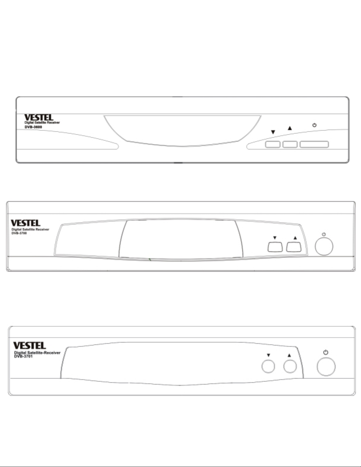
SAT 3600
SAT 3700
SAT 3701
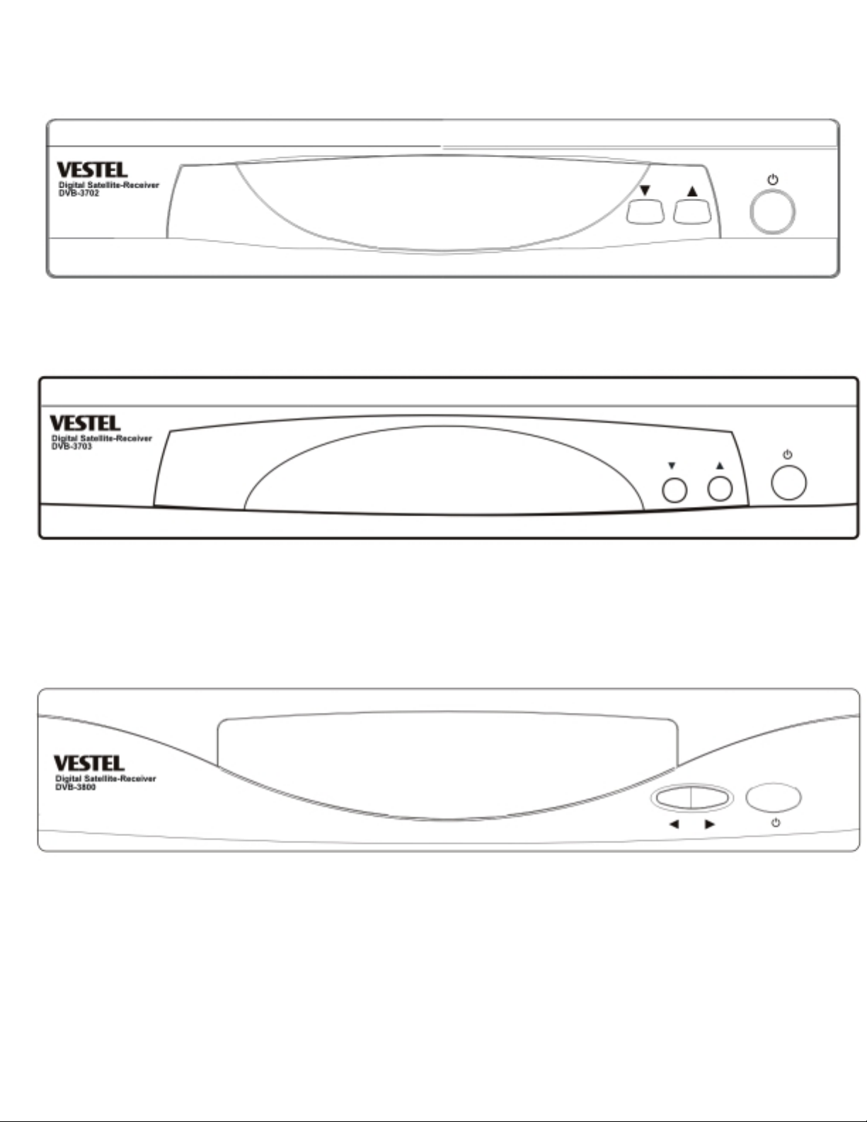
SAT 3702
SAT 3703
SAT 3800
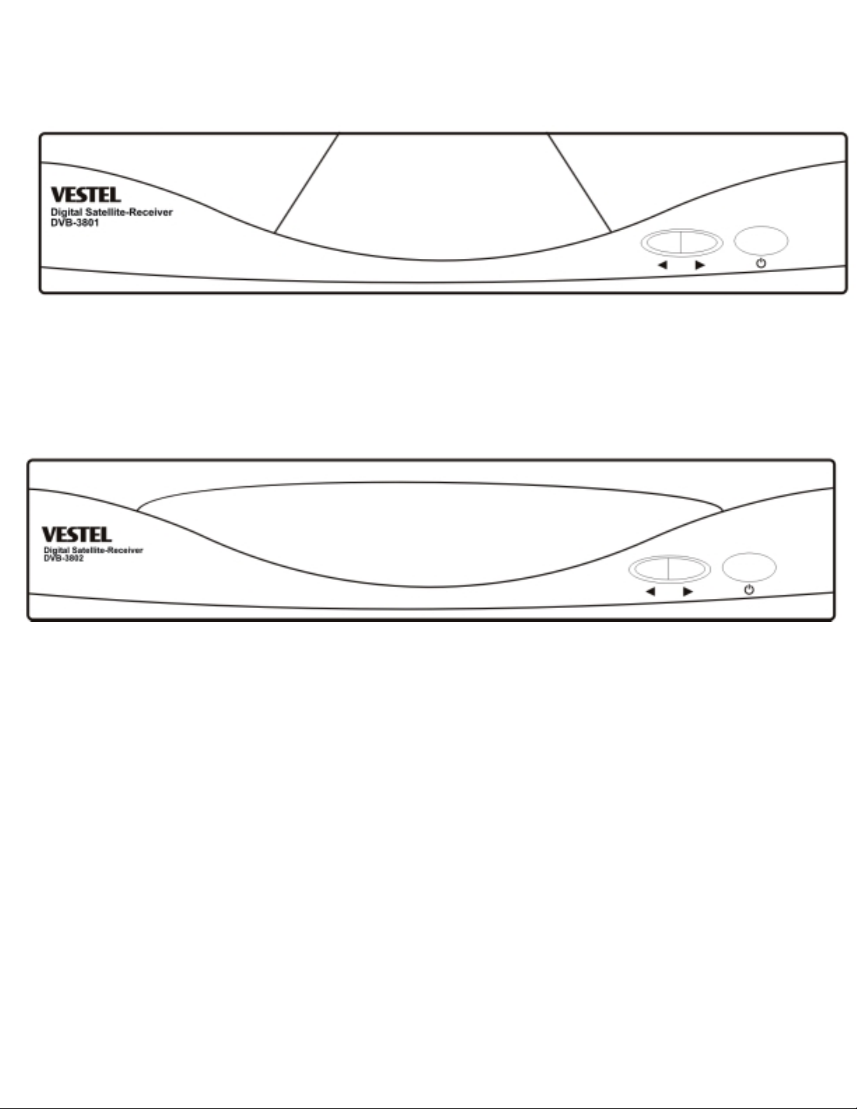
SAT 3801
SAT 3802
Page 2
SERVICE MANUAL
SATELLITE STB MODELS
Rev 1.0 21.10.02 16:23 Page 2
Page 3
SERVICE MANUAL
Rev 1.0 21.10.02 16:23 Page 3
Page 4
SERVICE MANUAL
Rev 1.0 21.10.02 16:23 Page 4
Page 5

SERVICE MANUAL
SATELLITE STB MODELS......................................................................................................................................................2
REVISION HISTORY .................................................................................................................................................................6
GENERAL DESCRIPTION........................................................................................................................................................7
I5518 (IC100)........................................................................................................................................................................7
ST
SDRAM 8MB
F
LASH MEMORY 1 MBYTE (IC301)........................................................................................................................................23
EEPROM
YTE (IC300)......................................................................................................................................................23
S 128K (16,384 X 8) 2-WIRE SERIAL (IC302).........................................................................................................25
USED IC LISTS .......................................................................................................................................................................... 33
CONNECTORS..................................................................................................................... ..................................................... 34
P
OWER CONNECTOR..................................................................................................................................................................34
F
RONT PANEL CONNECTOR ....................................................................................................................................................... 34
5512 JTAG C
ONNECTORS.........................................................................................................................................................34
SCART CONNECTION........................................................................................................................................................... 35
TV S
CART SOCKET...................................................................................................................................................................35
CART SOCKET................................................................................................................................................................36
VCR S
RS232 S
RCA (A
ERIAL PORT..................................................................................................................................................................36
UDIO AND COMPOSITE VIDEO) CONNECTOR................................................................................................................. 36
POWER REQUIREMENTS......................................................................................................................................................37
PCB EXPLANATIONS..............................................................................................................................................................37
INTRODUCTION................................................................................................................................................................... 37
POWER BOARD (16PW07 E3) ............................................................................................................................................ 37
MAIN BOARD (16MB07 E3 ) ............................................................................................................................................... 38
FRONT PANEL BOARD (TK507-2)....................................................................................................................................39
SERVICE MENU INTERFACE...............................................................................................................................................40
RF M
ODULATOR SYSTEM :........................................................................................................................................................40
ODULATOR TYPE : ............................................................................................................................................................ 40
RF M
T
UNER TYPE :............................................................................................................................................................................40
S
CARTS :.................................................................................................................................................................................... 40
R
EBOOT :................................................................................................................................................................................... 40
C
LEAR DATABASE :...................................................................................................................................................................41
L/R: DBC
OWNLOAD PGM : ...................................................................................................................................................................42
D
R
EMOTE/FRONT TEST : .............................................................................................................................................................. 42
7-S
S
YSTEM DIAGNOSTIC :............................................................................................................................................................... 43
D
EVELOPMENT TEAM :..............................................................................................................................................................43
U
PLOAD DEFAULT SAT_XPDRS :...............................................................................................................................................43
OWNLOAD DEFAULT SAT_XPDRS :......................................................................................................................................... 43
D
R
S232 TEST :.............................................................................................................................................................................44
OPY – OK: UPLOAD PGM :....................................................................................................................................... 41
EGMENT DISPLAY TEST :......................................................................................................................................................43
SOFTWARE UPGRADE THROUGH RS232.........................................................................................................................45
SCHEMATICS............................................................................................................. ERROR! BOOKMARK NOT DEFINED.
BILL OF MATERIALS.............................................................................................................................................................48
BOARD LAYOUT.......................................................................................................ERROR! BOOKMARK NOT DEFINED.
Rev 1.0 21.10.02 16:23 Page 5
Page 6

SERVICE MANUAL
REVISION HISTORY
Rev 1.0 07/25/02 Tuncay Akkurt Initial Revision
Schematics
Rev 1.0 21.10.02 16:23 Page 6
Page 7

SERVICE MANUAL
GENERAL DESCRIPTION
Major functional blocks are discussed briefly in this section. A more detailed description is contained later in the
document.
STi5518 (IC100)
1. Introduction
The STi5518 integrates in a single chip: a transport dem ultiplex block; an ST20 32-bit system CPU; an
audio/video MPEG2 decoder; display and gr aphics features; a digi tal video encoder; and s ystem peripherals. The
Sti5518 integrates D irecTV and D VB desc ram blers in the tra nsport demultip lex block , allowin g it to be used in b oth
Digital Video Broadcasting (DVB) and Digital Satellite System (DSS) set-top box applications.
2. Technical Specification
Integrated 32-bit host CPU up to 81 MHz
2 Kbytes of Icache, 2 Kbytes of Dcache, and 4 Kbytes of SRAM configurable as Dcache.
Audio decoder
5.1 channel Dolby Digital® /MPEG-2 multi-channel decoding, 3 X 2-channel PCM outputs
IEC60958 -IEC61937 digit al out put
SRS®/TruSurround®
DTS® digital out and MP3 decoding
Alignment beep for satellite dishes.
Video decoder
Supports MPEG-2 MP@ML
Fully programmable zoom-in and zoom-out
NTSC to PAL conversion.
DVD and SVCD subpicture decoder
High performance on-screen display
2 to 8 bits per pixel OSD options
Anti-flicker, anti-flutter and anti-aliasing filters.
PAL/NTSC/SECAM encoder
RGB, CVBS, Y/C and YUV outputs with 10-bit DACs
Macrovision® 7.01/6.1 compatible (optional).
Shared SDRAM memory interface
1 or 2x16-Mbit, or 1x64-Mbit 125 MH
Programmable CPU memory interface for SDRAM, ROM, peripherals...
Front-end interface
DVD, VCD, SVCD and CD-DA compatible
Z SDRAM.
Rev 1.0 21.10.02 16:23 Page 7
Page 8

SERVICE MANUAL
Serial, parallel and ATAPI int er f ac es
Hardware sector filtering
Integrated CSS decryption and track buffer.
Hardware transport-stream demultiplexor
Parallel/serial input
DES and DVB descramblers
32 PID support.
Integrated peripherals
2 UARTs, 2 SmartCards, I
2C controller, 3 PWM outputs, 3 capture timers
Modem support
44 bits of programmable I/O
IR transmitter/receiver.
Professional toolset support
ANSI C compiler and libraries.
208 pin PQFP package.
The STi5518 is a hig hly integrated single-chip deco der, d es ig ned f or use in feature-rich mass-market set-top boxes.
It integrates a high-performance 32-bit CPU, a dedicated block for DVB/DirecTV transport demultiplexing and
descrambling, modules for MPEG-2 video and audio decoding with 3D-surround and MP3 support, advanced
display and graphics features, a digital video encoder and all of the system peripherals required in a typical low-cost
interactive receiv er. To cover t he needs of DVD-capable s et-top boxes , ST i5518 integr ation opt ions incl ude a CS S
decryption block, a Dolby Digital audio decoder and Macrovision copy protection. An ATAPI interface is built-in,
supporting the glueles s c onnection of s tandar d Hard Dis k Drives. I n this wa y, the ST i551 8 is id eal for set- top boxes
featuring trick modes such as live TV recording , pausing and time-shif ting. The STi5518 is backward compatible
with the popular STi5500 set-t op box deco der, all owing eas y migrat ion from the previous generation. T he high level
of integration in a single PQFP-2 08 pac kage makes the STi5518 ideally suited fo r lo w-c os t, h ig h-vol ume set-top box
applications.
Rev 1.0 21.10.02 16:23 Page 8
Page 9

SERVICE MANUAL
3. Architecture overview
The figure below shows the architecture of the Sti5518.
This chapter gives a brief overview of each of the functional blocks of the STi5518.
4. STi5518 functional modules
a. Central processor
The STi5518 Central Processing Unit is a ST20C2+ 32-bit processor core. It contains instruction processing logic,
instruction and data pointers, and an operand regist er. It directly accesses the high-s peed on-chip SRAM, which
can store data or programs and uses the cache to reduce access time to off-chip program and data memory.
The processor can access memory via the Programmable CPU Interface (often referred to as the EMI) or the
Shared Memory Interface (SMI), which is shared with the video, audio, sub-picture and OSD decoders.
Rev 1.0 21.10.02 16:23 Page 9
Page 10

SERVICE MANUAL
b. MPEG video decoder
This is a real-time video compression processor supporting the MPEG-1 and MPEG-2 standards at video rates up t
720 x 480 x 60 Hz and 720 x 576 x 50 Hz. Picture format conversion for display is performed by vertical and
horizontal filters. User- defined bitmaps can be super -impos ed on the d isplay pictur e b y using the on- screen d isplay
function. The display unit is part of the MPEG vide o decoder, it overla ys the f our displa y planes shown i n the figure
below. The display planes are norm ally overlaid in the ord er illustrated, with the background color at the back and
the sub-picture at the f ront (us ed as a curs or p lane). T he s ub-pic ture pla ne ca n a ltern ativel y be posi tioned bet ween
the OSD and MPEG video planes where it can be used as a second on-screen display plane.
c. Audio decoder
The audio decoder accepts: Dolby Digital, MPEG-1 layers I, II and III, MPEG-2 layer II 6-channel, PCM, CDDA data
formats; MPEG2 PES streams for MPEG-2, MPEG-1, Dolby Digital, MP3, and Linear PCM (LPCM). The audio
decoder supports DTS® digital out (DVD DTS and CDDA DTS). SPDIF input data (IEC-60958 or IEC-61937
standards) is accepted if an external circuitry extr acts the PCM clock from the str eam. Skip frame, repeat block s
and soft mute frame features can be used to synchronize audio and video data. PTS audio extraction is also
supported. The devic e outputs up to 6 channels of PCM data and appr opriate clocks for ex ternal digital-to-anal og
converters. Program mable downmix enables 1,2, 3 or 4 channel outputs. D ata can be output in either I²S f ormat or
Sony format. The decoder can form at output data according t o IEC-60958 s tandard (for non c ompress ed data: L/R
channels, 16, 18, 20 an d 24-bits) or IEC-6193 7 standar d (for com pres sed data), for F
or 32 kHz. Sampling frequenc i es of 96 kHz, 48 kHz, 44.1 kHz, 32 kHz and half sampling frequencies are supported.
A downsampling f ilter (9 6 kHz/48 kHz) is available. T he decoder supports dual mode for MPEG an d Do lby Digital. It
includes a Dolby surround compatible downmix and a ProLogic decoder. A pink noise generator enables the
accurate positioning of speakers for optim al surround sound s etup. PCM be ep tone is a s pecial m ode used for S et
Top Box. It generates a triangular signal of variable frequency and amplitude on the left and right channels. In
global mute mode, the decoder decodes the incoming bitstream normally but the PCM and SPDIF outputs are
softmuted. This mode is used to prepare a period of decoding mode, to synchronize audio and video data without
hearing the audio. S low-forward and fast-forward tr ick modes are available f or compressed and n on-compressed
data. The control interface of the decoder is activated via memory mapped registers in the ST20 address space.
S = 96 kHz, 48 kHz, 44.1 k Hz
d. IR transmitter/receiver
The STi5518 provides a pulse-position modulated signal for automatic VCR programming by the set-top box. The
signal is output to the IR blast pin and an accessory jack pin, simultaneously. The pulse frequency, number of
pulses (envelope length) and the total cycle time is controlled by registers.
e. Modem analog front-end interface
The Modem Analog Front- end interface is used to trans fer transmit and receive D AC and ADC samples bet ween
the memory and an external modem analog front-end (MAFE), using a synchronous serial protocol. DMA is used to
transfer the sample data between memory buffers and the MAFE interface module, with separate transmit and
receive buffer s and double buf fering of the buf fer pointer s. FIFOs are us ed to tak e into account the ac cess laten cy
to memory, in a worst c ase system and to all ow the use of bursts for m emory bandwidth eff iciency improvem ent.
The V22 bis standard is supported.
f. Memory subsystem
On-chip
The on-chip memory includes 2K bytes of instruction c ache, 2Kbytes of data cache and 4 Kbytes of SRAM th at can
be optionally configured as data cache. The subsystem provides 240M/bytes of internal bandwidth, supporting
pipelined 2- cycle internal m emory access. The instruction a nd data caches are direct-m apped, with a write-back
system for the data-c ache. The caches support bur st accesses to the external memories for refill and write-back.
Burst access increases the performance of pagemode DRAM memories.
Off-chip
There are two off-chip memory interfaces:
• The external memory interface (EMI) accessed by the ST20 is used for the transfer of data and programs
between the STi5518 and external peripherals, flash and additional SDRAM and DRAM.
Rev 1.0 21.10.02 16:23 Page 10
Page 11

SERVICE MANUAL
• Shared memory interface (SMI) controls the movement of data between the STi5518 and 16, 32 or 64 Mbits of
SDRAM. This external SDRAM stores the display data generated by the MPEG decoder and CPU and the C2+
code data.
The EMI uses minimal external support logic to support memory subsystems, and accesses a 32 Mbytes of physical
address space (greater if SDRAM or DRAM is used) i n four ge nera l purpos e m emor y banks of 8 or 16 b its wide, 21
or 22 address lines, an d byte select. F or applications req uiring extra m emory, the EMI su pports this extra memor y
with zero external support logic , even for 16-bit SDRAM devices. The EMI c an be configured for a wide variety of
timing and decode functions b y the conf igurat ion regis ters. The t im ing of each of the four m em or y banks c an be set
separately, with different device types being placed in each bank with no need for external hardware.
g. Serial communication
Asynchronous serial controllers
The Asynchronous Serial Controller (ASC), also referred to as the UART interface, provides serial communication
between the STi5518 and other microcontrollers, microprocessors or external peripherals. The STi5518 has four
ASCs, two of which are generally used by the SmartCard controllers.
Eight or nine bit data transfer, parity generation, and the number of stop bits are programmable. Parity, framing, and
overrun error detection increase data transfer reliability. Transmission and reception of data can be double-buffered,
or 16-deep FIFOs can be used. A mechanism to distinguish the address from the data bytes is included for
multiprocessor comm unication. Testing is supported by a loop-back option. A 16-bit baud-rate generator provides
the ASC with a separate serial clock signal.
Two ASCs support full-duplex and 2 half-duplex asynchronous communication, where both the transmitter and the
receiver use the same data fram e format and the sam e baud rate. Each A SC can be set to operate in SmartCard
mode for use when interfacing to a SmartCard.
Synchronous serial controller
Two Synchronous Serial Controllers (SSC) provide high-speed interfaces to a wide variety of serial memories,
remote control recei vers and other microcontrol lers. The SSCs support all of the features of the Serial Peripher al
Interface bus (SPI) a nd the I
SSCs share pins with the parallel input/output (PIO) ports, and support half-duplex synchronous communication.
h. Front-end interface
The STi5518 can be connected to a front-end through the following interfaces:
2C bus. The SSCs c an be program med to interf ace to other serial b us standar ds. The
• I2S interface;
• multi-format serial interface;
• multi-format parallel interface;
• ATAPI interface (for Hard Disk Drives and DVD-ROMs)
i. On-chip PLL
The on-chip PLL accepts 27 MHz input and generates all the internal high-frequency clocks needed for the CPU,
MPEG and audio subsystems.
j. Diagnostic controller (DCU)
The ST20 Diagnostic Controller Unit (DCU) is used to boot the CP U and to c ontro l a nd monitor the chip systems via
the standard IEEE 1194.1 Test Acc ess Port. The DCU includes on-chip hard ware with ICE (In Circuit Emulation)
and LSA (Logic State Analyzer) featur es to facilitate verificati on and debugging of softwar e running on the on-c hip
CPU in real time. It is an independent hardware module with a private link from the host to support real-time
diagnostics.
k. Interrupt subsystem
The interrupt system allows an on-chip module or external interrupt pin to interrupt an active process so that an
Rev 1.0 21.10.02 16:23 Page 11
Page 12

SERVICE MANUAL
interrupt handling process can be run. An interrupt can be signalled by one of the following: a signal on an external
interrupt pin, a signal from an internal peripheral or subsystem, software asserting an interrupt in the pending
register. Interrupts are im plemented by an on-chip interrupt controll er and an on-ch ip interrupt-level co ntroller. The
interrupt controller s upports eight prioritized inter rupts as inputs and manag es the pending interrupts. Th is allows
the nesting of pre-em ptive interrupts for real-time system design. Each interrupt can be programmed to be at a
lower or higher priority than the high priority process queue.
l. PAL/NTSC/SECAM encoder
The integrated digital encoder converts a multiplexed 4:2:2 or 4:4:4 YCbCr stream into a standard analog baseband
PAL/NTSC or SECAM signal and into RGB, YUV, Yc and CV BS components. The encoder can perform closedcaption, CGMS encoding, and a ll o ws M ac rovision
TM 7.01/6.1 copy protection. The DENC is able to encode Tele tex t
according to the “CCIR/ITU-R Broadcast Teletext System B” specification, also known as “World System Teletext”.
In DVB applicatio ns, Teletext data is em bedded within D VB stream s as MPEG d ata packets . It is the respons ibility
of the software to han dle incoming data p ackets and in partic ular to store T eletext packets in a buf fer, which the n
passes them to the DENC on request.
m. SmartCard interfaces
Two SmartCard interfaces support SmartCards compliant with ISO7816-3. Each interface is has a UART (ASC), a
dedicated programmable clock generator, and eight bits of parallel IO port.
n. PWM and counter module
The PWM and counter module provides three PWM encoder outputs, three PWM decoder (capture) inputs and four
programmable timer s. Each capt ure input can be programmed to detect r ising edge, falling edge, both edges or
neither edge (disabled) . These facilities are c locked by two indep endent clocks , one for PWM outputs and one for
capture inputs/timers. The PWM counter is 8-bit, with 8-bit registers to set the output-high time. The
capture/compare counter and the compare and capture registers are 32-bit. The module generates a single
interrupt signal.
o. Parallel I/O module
44 bits of parallel I/O are configured in 6 ports, and each bit is programmable as output or input. The output can be
configured as a totem-pole or open- drain driver. The input com pare logic can ge nerate an interr upt on any chan ge
of any input bit. Many parallel IO have alt ernate functions and can be connected to an int ernal peripheral signal
such as a UART or SSC.
Rev 1.0 21.10.02 16:23 Page 12
Page 13
SERVICE MANUAL
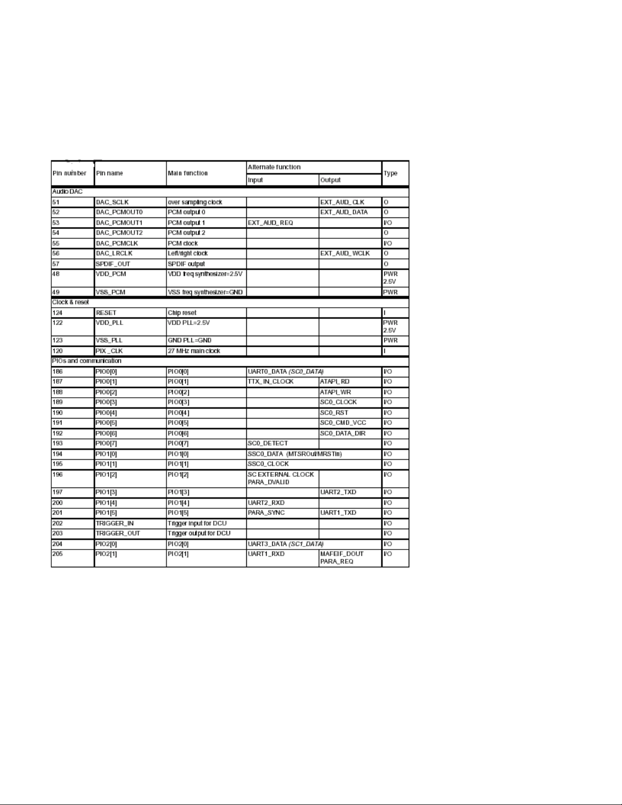
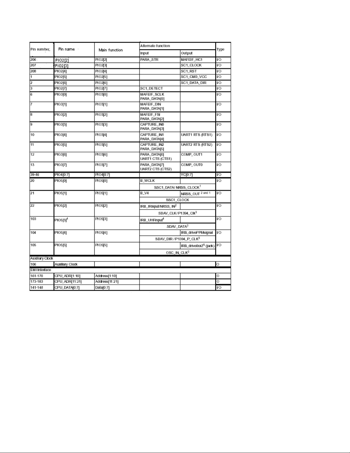
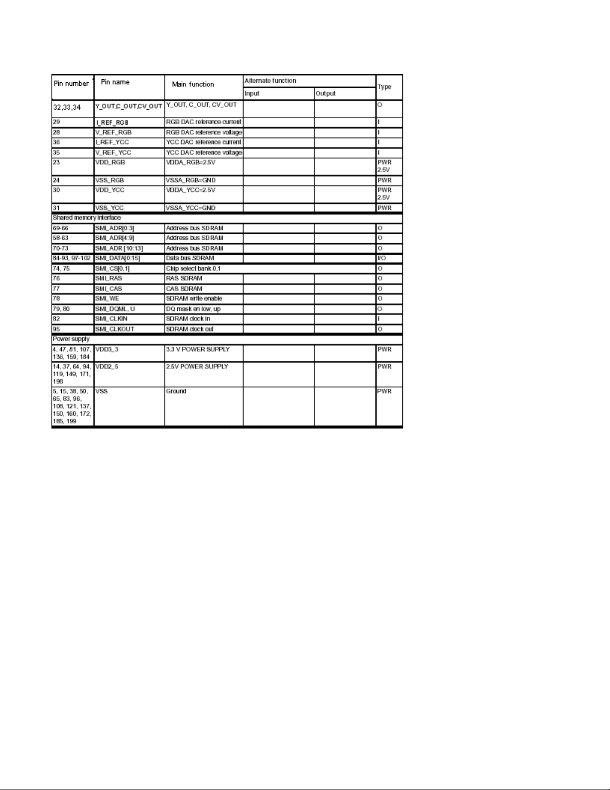
5. Pin list sorted by function
Alternate functions printed in Italic show a suggested use of the PIO; alternate functions not printed in Italic are
multiplexed with a specific hardware.
Rev 1.0 21.10.02 16:23 Page 13
Page 14
SERVICE MANUAL
Rev 1.0 21.10.02 16:23 Page 14
Page 15

SERVICE MANUAL
Rev 1.0 21.10.02 16:23 Page 15
Page 16
SERVICE MANUAL
1. FEI_CFG bits 8 and 9 must be programmed according to the required NRSS configuration.
2. The NRSS_IN and NRSS_OUT pins are swapped around on the STi5518 compared to the STi5508.
3. Register LNK_SDAV_CONF bit 22 (SDE) must be set to 1 to validate the output path.
4. Inverted. ATTENTION! the PIO input is also inverted.
5. The PIO must be configured in open drain.
6. BOOT_FROM_ROM is active during reset.
7. Tie low whenever JTAG is not used.
Rev 1.0 21.10.02 16:23 Page 16
Page 17

SERVICE MANUAL
6. Pins sorted by pin number
Rev 1.0 21.10.02 16:23 Page 17
Page 18

SERVICE MANUAL
Rev 1.0 21.10.02 16:23 Page 18
Page 19

SERVICE MANUAL
Rev 1.0 21.10.02 16:23 Page 19
Page 20

SERVICE MANUAL
Rev 1.0 21.10.02 16:23 Page 20
Page 21

SERVICE MANUAL
Rev 1.0 21.10.02 16:23 Page 21
Page 22

SERVICE MANUAL
1. FEI_CFG bits 8 and 9 must be programmed according to the required NRSS configuration.
2. The NRSS_IN and NRSS_OUT pins are swapped around on the STi5518 compared to the STi5508.
3. Register LNK_SDAV_CONF bit 22 (SDE) must be set to 1 to validate the output path.
4. Inverted. ATTENTION! the PIO input is also inverted.
5. The PIO must be configured in open drain.
6. Tie low whenever JTAG is not used
7. BOOT_FROM_ROM is active during reset.
Rev 1.0 21.10.02 16:23 Page 22
Page 23

SERVICE MANUAL
SDRAM 8MByte (IC300)
FEATURES
• PC66-, PC100- and PC133-compliant
• Fully synchronous; all signals registered on positive edge of system clock
• Internal pipelined operation; column address can be
changed every clock cycle
• Internal banks for hiding row access/ precharge
• Programmable burst lengths: 1, 2, 4, 8 or full page
• Auto Precharge, includes CONCURRENT AUTO
PRECHARGE, and Auto Refresh Modes
• Self Refresh Modes: standard and low power
• 64ms, 4,096-cycle refresh
• LVTTL-compatible inputs and outputs
• Single +3.3V ±0.3V power supply
GENERAL DESCRIPTION
The 64Mb SDRAM is a high-speed CMOS, dynamic random-access memory containing 67,108,864 bits. It is
internally configured as a quad-bank DRAM with a synchronous interface (all signals are registered on the positive
edge of the clock signal, CLK). Each of the x4’s 16,777,216 -bit banks is organized as 4,096 rows by 1,024 columns by 4
bits. Each of the x8’s 16,777,216-bit banks is organized as 4,096 rows by 512 columns by 8 bits. Each of the x16’s
16,777,216-bit banks is organized as 4,096 rows by 256 columns by 16 bits. Read and write accesses to the
SDRAM are burst oriented; accesses start at a selected location and continue for a programmed number of
locations in a progr ammed sequenc e. Accesses begi n with the registr ation of an ACT IVE command, which is then
followed by a READ or WRITE
command. The address bits registered coincident with the ACTIVE command are used to select the bank and row to be
accessed (BA0, BA1 select the bank; A0-A11 select the row). The address bits registered coincident with the READ or
WRITE command are used to select the starting column location for the burst access.
The SDRAM provides for programmable READ or WRITE burst lengths of 1, 2, 4 or 8 locations, or the full page,
with a burst terminate option. An AUTO PRECHARGE function may be enabled to provide a self-timed row precharge that
is initiated at the end of the burst sequence. The 64Mb SDRAM uses an internal pipelined architecture to achieve highspeed operation. This architecture is compatible with the 2n rule of prefetch architectures, but it also allows the column
address to be changed on every clock cycle to achieve a high-speed, fully random access. Precharging one bank while
accessing one of the other three banks will hide the precharge cycles and provide seamless, high-speed, random-access
operation. The 64Mb SDRAM is designed to operate in 3.3V, lowpower memory systems. An auto refresh mode is
provided, along with a power-saving, power-down mode. All inputs and outputs are LVTTL-compatible. SDRAM’s offer
substantial advances in DRAM operating performance, including the ability to synchronously burst data at a high data rate
with automatic column-address generation, the ability to interleave between internal banks in order to hide precharge time
and the capability to randomly change column addresses on each clock cycle during a burst access.
Flash Memory 1 MByte (IC301)
Low Voltage Single Supply Flash Memory
2.7V to 3.6V SUPPLY VOLTAGEfor
PROGRAM, ERASE and READ OPERATIONS
FASTACCESS TIME: 90ns
FASTPROGRAMMING TIME
– 10µs by Byte / 20µs by Word typical
PROGRAM/ERASE CONTROLLER (P/E.C.)
– Program Byte-by-Byte or Word-by-Word
– Status Register bits and Ready/Busy Output
MEMORY BLOCKS
– Boot Block (Top or Bottom location)
– Parameter and Main blocks
Rev 1.0 21.10.02 16:23 Page 23
Page 24

SERVICE MANUAL
BLOCK, MULTI-BLOCK and CHIP ERASE
MULTI BLOCK PROTECTION/TEMPORARY
UNPROTECTION MODES
ERASE SUSPEND and RESUME MODES
– Read and Program another Block during
Erase Suspend
LOW POWER CONSUMPTION
– Stand-byand AutomaticStand-by
100,000 PROGRAM/ERASE CYCLES per
BLOCK
20 YEARSDATARETENTION
– Defectivity below 1ppm/year
ELECTRONIC SIGNATURE
– Manufacturer Code: 0020h
– Device Code, M29W800T: 00D7h
– Device Code, M29W800B: 005Bh
DESCRIPTION
The M29W800 is a non-volatile memory that may be erased electrically at the block or chip level and programmed
in-system ona Byte-by-Byteor Wordby-Word basis using only a single 2.7V to 3.6V V
CC supply. For Program and
Erase operations the necessary high voltages are generated internally. The device can also be programmed in
standard programmers. The array matrix organisation allows each block to be erased and reprogrammed without
affecting other blocks. Blocks can be protected against programing and erase on programming equipment, and
temporarily unprotected to make changes in the application. Each block can be programmed and erased over
100,000 cycles. Instructions for Read/Reset, Auto Select for reading the Electronic Signature or Block Protection
status, Programming, Blockand Chip Erase, Erase Suspend and Resume are written to the device in cycles of
commands to a Command Interface using standard microprocessor write timings. The device is offered in
TSOP48(12 x 20mm) and SO44 packages. Both normal and reverse pinouts are available for the TSOP48package.
Organisation
TheM29W800 is organised as 1 Mx8 or 512K x16 bits selectable by the BYTE signal. When BYTEis Low the Bytewide x8 organisation is selected and the address lines are DQ15A–1 and A0-A18. The Data Input/Output signal
DQ15A–1 acts as address line A–1 which selects the lower or upper Byte of the memory word for output on DQ0DQ7,DQ8-DQ14 remain at High impedance. When BYTEis High the memory uses the address inputs A0-A18 and
the Data Input/Outputs DQ0-DQ15. Memory control is provided by Chip Enable E, Output Enable G and Write
EnableW inputs. AReset/Block Temporary Unprotection RPtri-level input provides a hardware reset when pulled
Low,and when held High (atV
ID) temporarily unprotects blocks previously protected allowing them to be programed
and erased. Erase and Program operations are controlled by an internal Program/Erase Controller (P/E.C.). Status
Register data output on DQ7 provides a Data Polling signal, and DQ6 and DQ2 provide Toggle signals to indicate
the state of the P/E.C operations. A Ready/Busy RB output indicates the completion of the internal algorithms.
Memory Blocks
The devices feature asymmetrically blocked architecture providing system memory integration. Both M29W800Tand
M29W800Bdeviceshavean array of 19 blocks, one Boot Block of 16 KBytes or 8KWords, two Parameter Blocks of 8
KBytes or 4KWords, one Main Block of 32 KBytes or 16KWordsand fifteen Main Blocks of 64 KBytes or 32KWords.
The M29W800Thas the Boot Block at the top of the memory address space and the M29W800B locates the Boot
Block starting at the bottom. The memory maps are showed in Figure3. Each block can be erased separately, any
combination of blocks can be specified for multi-block erase or the entire chip may be erased. The Erase operations
are managed automatically by the P/E.C. The block erase operation can be suspended in order to read from or
program to any block not being ersased, and then resumed. Block protection provides additional data security. Each
block can be separately protected or unprotected against Program or Erase on programming equipment. All
previously protected blocks can be temporarily unprotected in the application.
Rev 1.0 21.10.02 16:23 Page 24
Page 25

SERVICE MANUAL
Bus Operations
The following operations can be performed using the appropriate bus cycles: Read(Array, Electronic Signature,
Block Protection Status), Write command, Output Disable, Standby, Reset, Block Protection, Unprotection,
Protection Verify, Unprotection Verify and Block Temporary Unprotection.
Command Interface
Instructions, made up of commands written in cycles, can be given to the Program/Erase Controller through a
Command Interface (C.I.). For added data protection, program or erase execution starts after4 or 6 cycles. The first,
second, fourth and fifth cycles are used to input Coded cycles to the C.I. This Coded sequence is the same for all
Program/Erase Controller instructions. The ’Command’ itself and its confirmation, when applicable, are given on the
third, fourth or sixth cycles. Any incorrect command or any improper command sequence will reset the device to
Read Array mode.
Instructions
Seven instructions are defined to perform Read Array, Auto Select (to read the Electronic Signature or Block
Protection Status), Program, Block Erase, Chip Erase, Erase Suspend and Erase Resume. The internal P/E.C.
automatically handles all timing and verification of the Program and Erase operations. The Status Register Data
Polling, Toggle, Error bits and the RB output may be read at any time, during programming or erase, to monitor
the progress of the operation. Instructions are composed of up to six cycles. The first two cycles input a Coded
sequence to the Command Interface which is common to all instructions The third cycle inputs the instruction setup command. Subsequent cycles output the addressed data, Electronic Signature or Block Protection Status for
Read operations. In order to give additional data protection, the instructions for Program and Block or Chip Erase
require further command inputs. For a Program instruction, the fourth command cycle inputs the address and data
to be programmed. For an Erase instruction (Block or Chip), the fourth and fifth cycles input a further Coded
sequence before the Erase confirm command on the sixth cycle. Erasure of a memory block may be suspended, in
order to read data from another block or to program data in another block, and then resumed. When power is first
applied or if V
CC falls below VLKO, the command interface is reset to Read Array.
EEPROMs 128K (16,384 x 8) 2-wire Serial (IC302)
Features
• Low-voltage and Standard-voltage Operation
– 5.0 (V
– 2.7 (VCC = 2.7V to 5.5V)
– 1.8 (V
• Internally Organized 16,384 x 8 and 32,768 x 8
• 2-wire Serial Interface
• Schmitt Trigger, Filtered Inputs for Noise Suppression
• Bidirectional Data Transfer Protocol
• 1 MHz (5V), 400 kHz (2.7V) and 100 kHz (1.8V) Compatibility
• Write Protect Pin for Hardware and Software Data Protection
• 64-byte Page Write Mode (Partial Page Writes Allowed)
• Self-timed Write Cycle (5 ms Typical)
• High Reliability
– Endurance: 100,000 Write Cycles
– Data Retention: 40 Years
– ESD Protection: > 4000V
• Automotive Grade and Extended Temperature Devices Available
• 8-pin JEDEC PDIP, 8-lead JEDEC and EIAJ SOIC, 14-lead TSSOP, and
8-pad Leadless Array Packages
Description
The AT24C128/256 provides 131,072/262,144 bits of serial electrically erasable and programmable read only
memory (EEPROM) organized as 16,384/32,768 words of 8 bits each. The device’s cascadable feature allows up to
four devices to share a common 2-wire bus. The device is optimized for use in many industrial and commercial
CC = 4.5V to 5.5V)
CC = 1.8V to 3.6V)
Rev 1.0 21.10.02 16:23 Page 25
Page 26

SERVICE MANUAL
applications where low-power and low-voltage operation are essential. The devices are available in space-saving 8pin JEDEC PDIP, 8-lead EIAJ, 8-lead JEDEC SOIC, 14-lead TSSOP, and 8-pad LAP packages. In addition, the
entire family is available in 5.0V (4.5V to 5.5V), 2.7V (2.7V to 5.5V) and 1.8V (1.8V to 3.6V) versions.
Pin Description
SERIAL CLOCK (SCL): The SCL input is used to positive edge clock data into each EEPROM device and negative
edge clock data out of each device.
SERIAL DATA (SDA): The SDA pin is bidirectional for serial data transfer. This pin is open-drain driven and may
be wire-O Red with any number of other open-drain or open collector devices.
DEVICE/PAGE ADDRESSES (A1, A0): The A1 and A0 pins are device address inpu ts that are hard wir ed or left not
connected for hardware compatibility with AT24C32/64. When the pins are hardwired, as many as four 128K/256K
devices may be addressed on a single bus system (device addressing is discussed in detail under the Device
Addressing section). When the pins are not hardwired, the default A
1 and A0 are zero.
WRITE PROTECT (WP): The write protect input, when tied to GND, allows normal write operations. When WP is
tied high to V
GND. Switching WP to V
CC, all write operations to the memory are inhibited. If left unconnected, WP is internally pulled down to
CC prior to a write operation creates a software write protect function.
Memory Organization
AT24C128/256, 128K/256K SERIAL EEPROM: The128K/256K is internally organized as 256/512 pages of 64-
bytes each. Random word addressing requires a 14/15-bit data word address.
Absolute Maximum Ratings
Operating Temperature.................................. -55°C to +125°C
Storage Temperature ..................................... -65°C to +150°C
Voltage on Any Pin
with Respect to Ground .....................................-1.0V to +7.0V
Maximum Operating Voltage .......................................... 6.25V
DC Output Current........................................................ 5.0 mA
Rev 1.0 21.10.02 16:23 Page 26
Page 27

SERVICE MANUAL
Tuner Alps (TU400)
Rev 1.0 21.10.02 16:23 Page 27
Page 28

SERVICE MANUAL
Rev 1.0 21.10.02 16:23 Page 28
Page 29

SERVICE MANUAL
Rev 1.0 21.10.02 16:23 Page 29
Page 30

SERVICE MANUAL
Rev 1.0 21.10.02 16:23 Page 30
Page 31

SERVICE MANUAL
Rev 1.0 21.10.02 16:23 Page 31
Page 32

SERVICE MANUAL
Rev 1.0 21.10.02 16:23 Page 32
Page 33

SERVICE MANUAL
USED IC LISTS
MAINBOARD (16MB07 E3)
MAX 232 (IC101) RS232 Driver/Receiver
Sti5518(IC100) Set Top Box Backend Decoder With Integrated Host Processor
TSH 22 (IC103) Dual Bipolar Operational Amplifier
M74HCU04 (IC102) Hex Inverter
MT48LC4M16A2 (IC300) 1 Mbyte x 16 x 4 banks SDRAM
M29W800T (IC301) Single Supply Flash Memory
M24C128 (IC302) 128Kbit Serial EEPROM
LM833 (IC501) Low Noise Dual Operational Amplifier
CS4335 (IC500) 8-Pin, 24 Bit, 96 KHz Stereo D/A Converter
DS1811 (IC400) Reset IC
NDS8947 (Q402) Dual P – Channel Enhancement Mode Field Effect Transistor
POWER BOARD (16PW07 E3)
TOP233Y (IC1) SMPS primary IC
SFH617A (IC2) Optocoupler
TL431(IC3) Programmable Precision Reference
LM358N (IC4) Low Power Dual Operantional Amplifier
LM7812 (IC5) 12V Voltage Regulator
Rev 1.0 21.10.02 16:23 Page 33
Page 34

SERVICE MANUAL
CONNECTORS
Power Connector
Power Connector – PL400
Pin Description
1LNB_SUPPLY_IN
2+30V
3+12 V
4GND
5GND
6+5 V
7+3V3
8+3V3
9H/V
10 LNB_POWER_ENABLE
11 DISEQC
Front Panel Connector
Front Panel Connector – PL401
Pin Description
1 STANDBY
2 SW3_STDBY
3GND
4 SW1_UP
5 SW1_DOWN
6GND
7IR_IN
85VFP
5512 JTAG Connectors
JTAG Connector – PL100
Pin Description Pin Description
1 ------ 11 TCK
2GND12GND
3 TRIGOUT 13 TDI
4GND14GND
5 TRIGIN 15 TDO
6GND16GND
7 ------ 17 JTAGRESET
8GND18GND
9TMS19TRST
10 GND 20 GND
Rev 1.0 21.10.02 16:23 Page 34
Page 35

SERVICE MANUAL
SCART CONNECTION
20 18 16 14 12 10 8 6 4 2
21 19 17 15 13 11 9 7 5 3 1
TV Scart Socket
TV Scart Socket – PL200
Pin Description Pin Description
1 Audio Right Output 12 No Connection
2 No Connection 13 GND
3 Audio Left Output 14 GND
4 GND 15 RED Output
5 GND 16 Fast Blanking Output
6 No Connection 17 GND
7
8 Function Switching Output 19 CVBS Output
9 GND 20 No Connection
10 No Connection 21 GND
11 GREEN Output
BLUE Output
18
GND
Rev 1.0 21.10.02 16:23 Page 35
Page 36

SERVICE MANUAL
VCR Scart Socket
VCR Scart Socket – PL200
Pin Description Pin Description
1
2 Audio Right Input 13 GND
3 Audio Left Output 14 GND
4 GND 15 No Connection
5 GND 16 No Connection
6 Audio Left Input 17 GND
7 No Connection 18 GND
8 Function Switching Input 19 CVBS Output
9 GND 20 CVBS Input
10 No Connection 21 GND
Audio
Right Output
12 No Connection
11
No Connection
RS232 Serial Port
RS232 Header – JK_DSUB_9
Pin Description Pin Description
1-2-
3TXD4CTS
5RXD6RTS
7-8-
9GND
RCA (Audio and Composite Video) Connector
A/V Connector – JK1
Pin Description
1 CVBS VIDEO
2 LEFT AUDIO
3 RIGHT AUDIO
Rev 1.0 21.10.02 16:23 Page 36
Page 37

SERVICE MANUAL
POWER REQUIREMENTS
Power measurements are for a board configured according to the included Bill of Materials while playing a
typical DVB channel.
16MB07 E3 Board
Power Consumption
Voltage Current mA Power
LNB_SUPPLY_IN (13V, 18V) ----- -----
+30V 1mA
+12V 30mA
STAND_BY
LNB_SUPPLY_IN (13V, 18V) 500mA (max)
POWER_ON
+5V 130mA
+3V3 ----- ----
Voltage Current mA Power
+30V 1mA
+12V 100mA
+5V 200mA
+3V3 960mA
Watts
Watts
PCB EXPLANATIONS
INTRODUCTION
DVB-S (digital satellite receiver) is designed with ST chipset. The technical information of
the receiver will be explained as three parts in the following pages: Power Board, Main Board
and Front Panel Board.
POWER BOARD (16PW07 E3)
The TOPSwitch concept is used for power supply. TOP 233Y (IC1) is designed to work
until 50 Watts in family of TOPSwitch_FX with 5 pins. The receiver works between 85 and 265
VAC mains voltage by using TOP 233Y in SMPS (Switch Mode Power Supply). The secondary
voltage regulation is adjusted by changing the duty cycle of drain signal according to the
feedback voltage, which is got from the secondary side of transformer. The feedback voltages
are 3.3V and 5V. This is connected to the comparator pin of TOP 233Y (IC1-pin1) via IC12
(Optocoupler). The comparator pin also protects the box against short circuits and overload. The
Vcc voltage of IC1 is between 2V –3V at pin2. The TOP 233Y works at a fixed frequency. This
frequency is fixed by RC oscillator at pin1. The pin3 and pin 4 are ground and the pin5 is drain
of MOSFET, which is inside the TOP 233Y.
Rev 1.0 21.10.02 16:23 Page 37
Page 38

SERVICE MANUAL
The switching of LNB supply voltage is done here. 18V and 22V outputs of transformer
switched by Q1, Q2 and H/V output of STV299 (TU400). By this way overheating and
unnecessary power consumption of Q5 (BD235) that regulates the LNB supply is prevented.
22kHz tone which is needed for DiSEqC signals, is generated at pin15 (Alps-TU400) or pin12
(Sharp-TU400) of STV0299 in tuner 22KHz is added to LNB supply here via LM358N (IC4).
16PW07-3 Power Board
Range of Voltage
Voltage Range of Voltage
LNB_SUPPLY_IN (13V, 18V) -----
+30V 31V – 34V
+12V 11.8V – 12.20V
+5V 4.7 V – 5.3V
STAND_BY
LNB_SUPPLY_IN (13V VER) 13 V – 14 V
LNB_SUPPLY_IN (18V HOR) 17V – 19V
POWER_ON
+3V3 3.6 V – 3.9V
Voltage Range of Voltage
+30V 31 V – 34 V
+12V 11.8 V – 12.2 V
+5V 4.8 V – 5.2 V
+3V3 3.3 V – 3.6V
+2V5 2.4 V – 2.7V
MAIN BOARD (16MB07 E3 )
The main board contains two parts: Front-end and Back-end. The digital signal is
demodulated in Front-end and then decoded in Back-end. Analog signals are processed in
different part.
The tuner (TU400 Alps or Sharp) is capable of getting both digital broadcasts. After the
modulated signals (I, Q outputs) receive from tuner, they go to STV0299 for demodulation
process in tuner. (TU400) In this IC, QPSK (Quadrated Phase Shift Keying) demodulation and
Forward Error Correction (FEC) are done which is necessary to demodulate DVB-S
transmission. TS (transport stream): The multiplexed digital stream which includes video, audio
and data information related to more than one channel (can be only one channel for SCPC
signals) and DVB tables. TS signals which are generated after demodulation, reach to Sti5518
(IC100) via 8 bits data bus. However, Byte Clock (TSIn_BCLK), Packet Clock (TSIn _STROUT)
signals are also sent to ST5518 (IC100) for demultiplexing process of TS. STV0299 is controlled
by I2C. In addition, 22kHz tone which is needed for DiSEqC signals, is generated at pin12 (Alps)
or pin10 (Sharp) of STV0299 in tuner.
LNB supply voltage (13/18V) is regulated via power board. Switching of supply voltage
between LOOP_IN and LNB_SUPPLY is done by Q402 transistors. The voltage on R403 is
proportional with the current of LNB supply. Overload on LNB supply increases the voltage on
R403, which results switching of Q400, Q401. By this way input LNB_OVERLOAD signal port of
Rev 1.0 21.10.02 16:23 Page 38
Page 39

SERVICE MANUAL
Sti 5518 (IC100) has the knowledge of LNB overload and then LNB supply is cut off for
protection of box via Sti 5518 port (P25).
At the backend part, there is a 32-bit CPU ST20 (in Sti 5518 embedded) that controls all
processes. Demultiplexer of the CPU provides the transmission of the desired channel’s
information from TS (Transport Stream) to MPEG Decoder section. The program that runs on
Sti5518 is in Flash memories (IC301). 8Mbits SDRAM (IC300) is used for data memory of this
program.
ST20 uses 32- bit data and 22- bit address buses for access to flash, DRAM and MPEG
decoder. It uses RAS, CAS etc. (read, write, enable) signals to activate related IC while
accessing them.
The clock which is needed by Sti 5518 (IC100), is generated at power on mode by
27MHz crystal (X100) and IC102 (74HCU04). The output of PWM outputs of Sti 5518 (IC100), is
filtered to have a DC level via R129 and C118. At the output of ICS3, the 27MHz clock can be
adjusted according to capacity of pins of 27MHz crystal to ground. This capacity is related with
DC value on D100 and D101 (BB133) at pins of crystal. This operation maintains
synchronization between audio-video that are coming from MPEG transport stream and PCR
clock.
Sti 5518 (IC100) can communicate any micro controller via RS232 by using IC101
(MAX232- RS232 level converter). The RS232 output of receiver is used for debug any problem
using Windows Hyper Terminal program.
MPEG decoder in Sti 5518 (IC100), is responsible for decoding of MPEG video and audio
signals. The video, which is compressed using MPEG2 and audio, which is compressed using
MPEG1 Layer 1-2, are processed here. After decoding, CCIR 601 formatted 8-bit video and
PCM formatted audio, are generated by mpeg decoder.
If digital broadcast has a teletext information, Sti 5518 (IC100) inserts teletext info into
VBI (vertical blanking interval) which can be watched on TV. Digital audio that is PCM formatted
on Sti 5518’ s output, is processed by CS4335 (IC500) and amplified by LM833 (IC501) and
then switched through IC200 (M74HC4052).
In digital mode, RGB signals are only delivered to TV scart. CVBS output is distributed
through IC201 (M74HC4052) to TV, AUX/VCR and VCR scarts. When VCR becomes active,
audio and video signals are driven to TV and VCR scarts, which is activated by pin8 of VCR
scart.
The program information is stored in 128Kbits EEPROM (24C128 – IC302) via I2C.
FRONT PANEL BOARD (TK507-2)
Rev 1.0 21.10.02 16:23 Page 39
Page 40

SERVICE MANUAL
To show program number, 4 digit 7 segment display (P2) is used on front panel board.
They are driven by 97C52 (IC502) which is controlled by MC. The functional keys are Standby,
Prog+, Prog-. IR module (IR01) is used for remote control.
FRONT PANEL PCBs
Functional Keys
Key Name Description
Standby
Prog +
Prog -
Standby
Program Up
Program Down
16FP05-2
Key Name
SW101
SW102
SW103
SERVICE MENU INTERFACE
There is a service menu for service person which is accessed by entering “MAIN MENU”
then pressing “9”, “2”, “9”, “5”, “2”, “6” keys on the remote control. You will see se rvice me nu
on the screen. This menu consists of fifteen active lines.
RF Modulator System :
You can control RF modulator system at this line. RF modulator system option can be
selected as Pal G or Pal I or Pal K type in software side by pressing left or right cursor key on
the remote control.
RF Modulator Type :
You can control RF modulator type at this line. RF modulator option can be selected as
Sharp or Samsung or LG type in software side by pressing left or right cursor key on the remote
control.
Tuner Type :
You can control Tuner type in software version at this line
Scarts :
You can control number of scarts in software version at this line
Reboot :
Rev 1.0 21.10.02 16:23 Page 40
Page 41

SERVICE MANUAL
You press OK button on the remote commander. Apparatus is restart.
Clear Database :
You press OK button on the remote commander. These settings reinitialize whole
EEPROM and store all programs erase.
L/R: DBCopy – OK: Upload PGM :
The object of this manual is to give necessary information and details to the user to
UPLOAD the program table to the receiver through RS232.
The list of the necessary equipment is as follows:
• Receiver and TV
• PC with “Hyper Terminal” function,
• RS232 serial communication cable (male to female modem cable).
Steps to be followed by the user are given below:
1. Connect the serial communication cable between the RS232 outport of the receiver and the
serial communication port (COM1 or COM2) of the PC.
2. Make sure that the PC is on and the receiver is in Power on mode.
3. Run “Hyper Terminal” program of the PC from Start / Programs / Accessories /
Communications / Hyper Terminal menu.
4. For a new connection, run Hypertrm.exe file.
5. Give a name and choose an icon for the connection. (You do not need to make a new
connection every time. You can use this name for the future connections.)
6. Choose communication port in the new coming window (COM1 or COM2) whichever you
have used in Step 1.
7. Port settings should be as follows:
Bits per second : 38400
Data Bits : 8
Parity : None
Stop bits : 1
Flow control : None
8. Now Hyper Terminal connection is established.
9. Go to “L/R: DBCopy – OK: Upload PGM” line on the service menu and press “LEFT” or
“RIGHT” keys of remote control (for copying database to the receiver). Please wait until the
print statements on the Hyper Terminal screen end.
10. From “Transfer” menu, choose “Receive File”.
11. Choose 1K Xmodem as protocol type.
12. “L/R: DBCopy – OK: Upload PGM” line on the service menu and press “OK” key of remote
control. Then Receive on of Hyper Terminal window and enter a file name like
(Program_table.pit) and press “OK” button. then You will see the progress on the PC
screen. Besides, on TV screen the receiver will count the downloaded packets.
Rev 1.0 21.10.02 16:23 Page 41
Page 42

SERVICE MANUAL
13. Wait for the transfer to be completed. Then, disconnect and exit from Hyper Terminal
window.
Download PGM :
The object of this manual is to give necessary information and details to the user to
upgrade the program table of the receiver through RS232.
The list of the necessary equipment is as follows:
• Receiver and TV
• PC with “Hyper Terminal” function,
• RS232 serial communication cable (male to female modem cable).
Steps to be followed by the user are given below:
1. Connect the serial communication cable between the RS232 outport of the receiver and the
serial communication port (COM1 or COM2) of the PC.
2. Make sure that the PC is on and the receiver is in Power on mode.
3. Go to “ Clear Database ” line and press “OK” key and then wait for twenty seconds (old
program table is deleted).
4. Run “Hyper Terminal” program of the PC from Start / Programs / Accessories /
Communications / Hyper Terminal menu.
5. For a new connection, run Hypertrm.exe file.
6. Give a name and choose an icon for the connection. (You do not need to make a new
connection every time. You can use this name for the future connections.)
7. Choose communication port in the new coming window (COM1 or COM2) whichever you
have used in Step 1.
8. Port settings should be as follows:
Bits per second : 38400
Data Bits : 8
Parity : None
Stop bits : 1
Flow control : None
9. Now Hyper Terminal connection is established. From “Transfer” menu, choose “Send File”.
10. Enter file name to be sent (program table).
11. Choose 1K Xmodem as protocol type.
12. Press Send button of Hyper Terminal window and then Go to “Download PGM” line on the
service menu and press “OK” key of remote control. You will see the progress on the PC
screen. Besides, on TV screen the receiver will count the downloaded packets.
13. Wait for the transfer to be completed. Then, disconnect and exit from Hyper Terminal
window.
Reset receiver by replugging in the mains cord of the set to the mains supply. Receiver will tune
to new program table.
Remote/Front Test :
Rev 1.0 21.10.02 16:23 Page 42
Page 43

SERVICE MANUAL
You press “OK” button remote commander to enter Remote/Front panel test then you can
see name of the button on the front panel or remote commander you pressed. By pressing Menu
button on the remote commander two times, you can exit.
7-Segment Display Test :
You press the OK key on the remote commander to start 7-segment display test. You
can see the test pattern on the display.
System Diagnostic :
You press the OK key on the remote commander and show your IC information in
apparatus main hardwar e
Development Team :
You press the OK key on the remote commander and Show your development team list
Upload Default Sat_Xpdrs :
This line can explain information under line
Download Default Sat_Xpdrs :
The object of this manual is to give necessary information and details to the user to
transmission the program table and preset table to the receiver through RS232.
The list of the necessary equipment is as follows:
• Receiver (master that sends the program table), TV
• Receiver (slave that receives the program table), TV
• RS232 serial communication cable (male to male modem cable).
Steps to be followed by the user are given below:
1. Connect the serial communication cable between the RS232 outport of the receiver to other
receiver.
2. Make sure that both receivers are in Power on mode.
3. Open the “main menu” and press “929526” keys sequentially for both of the receivers, you
will see service menu on the TV screens.
4. Go to “L/R: DBCopy – OK: Upload PGM” line on the service menu for master receiver and
press “LEFT” or “RIGHT” keys of remote control (for copying database to the receiver).
5. Go to “Download PGM” line on the service menu for slave receiver
6. “L/R: DBCopy – OK: Upload PGM” line on the service menu and press “OK” key of remote
control for master device. “Download PGM” line on the service menu and press “OK” key of
remote control for slave device. Besides, on TV screen the receiver will count the
downloaded packets.
7. Wait for the transfer to be completed the program table for both receivers.
8. Power off both receivers then power on them.
Rev 1.0 21.10.02 16:23 Page 43
Page 44

SERVICE MANUAL
9. Open the “main menu” and press “929526” keys sequentially for both of the receivers, you
will see service menu on the TV screens.
10. Go to “Upload default Sat_Xpdrs” line on the service menu for master receiver.
11. Go to “Download default Sat_Xpdrs” line on the service menu for slave receiver
12. “Upload default Sat_Xpdrs” line on the service menu and press “OK” key of remote control
for master device. “Download default Sat_Xpdrs” line on the service menu and press “OK”
key of remote control for slave device. Besides, on TV screen the receiver will count the
downloaded packets.
13. Wait for the transfer to be completed the preset table for both receivers.
Rs232 Test :
You connect the jumper to Rx output and Tx output. You press the “OK” key on the
remote commander then you can see “tESt” at the front display. You release the “OK” key on the
remote commander
then you can see “Err” at the front display.
You can return to main menu by pressing “Menu” keys on the remote control
Rev 1.0 21.10.02 16:23 Page 44
Page 45

SERVICE MANUAL
SOFTWARE UPGRADE THROUGH RS232 FOR HAVİNG 7-SEGMENT
DISPLAY MODELS
The object of this manual is to give necessary information and details to the user to
upgrade the software of the receiver through RS232.
The list of the necessary equipment is as follows:
Receiver and TV
PC with “Hyper Terminal” function,
RS232 serial communication cable (male to female modem cable).
Steps to be followed by the user are given below:
1. Connect the serial communication cable between the RS232 out port of the receiver and the
serial communication port (COM1 or COM2) of the PC.
2. Make sure that the PC is on and the receiver is in the Standby mode.
3. Run “Hyper Terminal” program of the PC from Start / Programs / Accessories /
Communications / Hyper Terminal menu.
4. For a new connection, run Hypertrm.exe file.
5. Give a name and choose an icon for the connection. (You do not need to make a new
connection every time. You can use this name for the future connections.)
6. Choose communication port in the new coming window (COM1 or COM2) whichever you
have used in Step 1.
7. Port settings should be as follows:
Bits per second : 115200
Data Bits : 8
Parity : None
Stop bits : 1
Flow control : None
8. Now Hyper Terminal connection is established. From “Transfer” menu, choose “Send File”.
9. Enter file name to be sent.
10. Choose Xmodem1K as protocol type.
11. Get the receiver out of standby mode using front panel keys just after pressing Send button
at the hyper terminal window. You will see the progress on the PC screen. Besides, front
panel display of the receiver will count the downloaded packets.
12. Wait for the transfer to be completed. Then, disconnect and exit from Hyper Terminal
window.
Receiver will automatically start to operate
Rev 1.0 21.10.02 16:23 Page 45
Page 46

SERVICE MANUAL
SOFTWARE UPGRADE THROUGH RS232 FOR HAVING LED MODELS
The object of this manual is to give necessary information and details to the user to
upgrade the software of the receiver through RS232.
The list of the necessary equipment is as follows:
Receiver and TV
PC with “Hyper Terminal” function,
RS232 serial communication cable (male to female modem cable).
Steps to be followed by the user are given below:
1. Connect the serial communication cable between the RS232 out port of the receiver and the
serial communication port (COM1 or COM2) of the PC.
2. Make sure that the PC is on.
3. Run “Hyper Terminal” program of the PC from Start / Programs / Accessories /
Communications / Hyper Terminal menu.
4. For a new connection, run Hypertrm.exe file.
5. Give a name and choose an icon for the connection. (You do not need to make a new
connection every time. You can use this name for the future connections.)
6. Choose communication port in the new coming window (COM1 or COM2) whichever you
have used in Step 1.
7. Port settings should be as follows:
Bits per second : 115200
Data Bits : 8
Parity : None
Stop bits : 1
Flow control : None
8. Now Hyper Terminal connection is established. From “Transfer” menu, choose “Send File”.
9. Enter file name to be sent.
10. Choose Xmodem1K as protocol type.
11. Plug in the mains cord of the set to the mains supply just after pressing Send button at the
hyper terminal window. You will see the progress on the PC screen. Besides, front panel
display of the receiver will count the downloaded packets.
12. Wait for the transfer to be completed. Then, disconnect and exit from Hyper Terminal
window.
Receiver will automatically start on standby mode. Af ter software initialisation(it takes 5 second)
finished you can turn on your digital set-top box by pressing one of the standby button, up/down
or numeric buttons on remote control or up/down/standby button on the front panel.
Rev 1.0 21.10.02 16:23 Page 46
Page 47

SERVICE MANUAL
Rev 1.0 21.10.02 16:23 Page 47
Page 48

SERVICE MANUAL
BILL OF MATERIALS
Ves.Code Description
20092206 MAINBOARD (MAN) SHARP
20092207 MAINBOARD (RAD) SHARP
20092208 MAINBOARD (SMD) SHARP
30000294 CAP SMD 100NF 50V K (0805) C427 C412 C413 C414 C244 C438 C265
30000814 RES SMD 1/10W 820R J R225 R233 R240 R246
30001734 JUMPER SMD (0805) S107 S108 S415 S416 S417 S418 S419
30001968 FERRITE BEAD (0805) BLM21B201S L106 L301 L302 L303 L304 L407 L400 L409
L410 L414 L208 L417 L418 L419 L420 L4 21 L422 L423
30007366 IC TSH22 (SO8) tape&reel IC103
30007378 IC LM 833(SO8) tape&reel IC501
30010689 DIODE VAR BB133 SMD D100 D101
30010780 IC 74HCU04 (SO14) tape&reel IC102
30010796 IC 24C128 SMD tape&reel IC302
30010817 IC MAX232 (SOIC16) IC101
30010822 IC M74HC4052 (SO16) tape&reel IC200 IC201
30012509 RES SMD 1/16W 100K J (0603) R502 R503
30012510 RES SMD 1/16W 100R J (0603) R108 R140 R147 R148 R254 R255 R411 R280 R281
30012551 TR BC847B SMD Q102 Q103 Q104 Q200 Q201 Q202 Q203 Q204 Q205 Q400 Q403
Q500 Q501 Q502 Q503 Q504 Q505 Q506 Q209 Q215 Q507 Q217
30012552 TR BC857B SMD Q100 Q101 Q105 Q206 Q207 Q208 Q212 Q401
30012559 CAP SMD 10PF 50V D COG (0603) C204 C208 C212 C216
30012560 CAP SMD 100PF 50V J (0603) C236 C220
30012564 CAP SMD 18PF 50V J (0603) C113 C116
30012567 CAP SMD 220PF 50V J (0603) C232 C234 C235 C243 C246
30012568 CAP SMD 270PF 50V J (0603) C502 C504
30012570 CAP SMD 330PF 50V J (0603) C119
30012573 CAP SMD 47PF 50V J (0603) C205 C206 C209 C210 C213 C214 C217 C218
30012581 CAP SMD 1NF 50V K R (0603) C221 C222 C228 C230 C238 C239 C241 C400 C401
C432 C433 C434 C435 C436 C240
30012582 CAP SMD 10NF 50V K R (0603) C100 C102 C104 C107 C114 C115 C409
30012583 CAP SMD 1.5NF 50V K (0603) C260
30012608 CAP SMD 27PF 50V J CH (0603) C515 C516
30012616 CAP SMD 2.7NF 50V K B (0603) C511 C512
30012641 RES SMD 1/16W 10K J (0603) R113 R114 R118 R119 R120 R121 R142 R300 R400
R401 R283 R512 R513 R514 R527 R292
30012650 RES SMD 1/16W 15K J (0603) R282
30012657 RES SMD 1/16W 1K J (0603) R134 R208 R211 R212 R213 R250 R251 R252 R253
R266 R267 R180 R518 R259 R214 R133 R135
30012658 RES SMD 1/16W 1M J (0603) R123
30012659 RES SMD 1/16W 2.2K J (0603) R110 R111 R402 R516 R539
30012667 RES SMD 1/16W 220K J (0603) R504 R510
30012668 RES SMD 1/16W 220R J (0603) R248 R519 R520 R521 R522 R523 R524 R525 R540
30012669 RES SMD 1/16W 22K J (0603) R128 R137 R138 R139 R218 R219 R220 R256 R257
R276 R277 R278 R279 R136 R287 R216 R273 R272 R271 R286 R290 R291
30012673 RES SMD 1/16W 270R J (0603) R249
30012677 RES SMD 1/16W 3.3K J (0603) R506 R509 R209
30012684 RES SMD 1/16W 330R J (0603) R224 R231 R238 R245
30012685 RES SMD 1/16W 33K J (0603) R404 R501 R507
30012692 RES SMD 1/16W 4.7K J (0603) R100 R109 R117 R505 R508 R526 R528 R529 R530
R531 R532 R533 R221 R228 R235 R242 R536 R537 R538 R541
Rev 1.0 21.10.02 16:23 Page 48
Page 49

SERVICE MANUAL
30012694 RES SMD 1/16W 470K J (0603) R124 R125
30012695 RES SMD 1/16W 470R J (0603) R227 R232 R241
30012696 RES SMD 1/16W 47K J (0603) R511 R500 R126
30012698 RES SMD 1/16W 5.6K J (0603) R515
30012702 RES SMD 1/16W 560R J (0603) R200 R201 R202 R203 R204 R205 R206 R207
30012707 RES SMD 1/16W 680R J (0603) R223 R229 R237 R243 R258 R222 R230 R236 R244
30012709 RES SMD 1/16W 7.5K J (0603) R217 R269 R270
30012712 RES SMD 1/16W 8.2K J (0603) R127 R129
30012713 RES SMD 1/16W 75R J (0603) R143 R226 R234 R239 R247
30012800 IC DAC CS4335 tape&reel IC500
30012982 RES SMD 1/16W 10R J 0603 R288 R289
30012985 JUMPER SMD 0603 S201 S203 S205 S300 S302 S304 S400 S401 S403 S404 S407
S411 S412 R116
30012986 RES SMD 1/16W 68R J 0603 R260
30014022 RES SMD 1/16W 47R J (0603) R103 R104 R105 R106 R130 R131 R144 R145 R517
30014088 IC SDRAM 4MX16 100MHZ tape&reel IC300
30014128 RES SMD 1/16W 33R J (0603) R112 R122 R132 R149 R151 R413 R414 R415 R184
R419 R420 R421 R422 R423 R424 R425 R416
30014342 IC TS87C52X2-MCB tape&reel IC502
30014344 TR NDS8947 IC402
30014442 RES SMD 1/16W 20K F(0603) R101 R102
30014714 IC DS1811(RESET IC) IC400
30014952 IC FLASH 8MB (TOP BOOT) tape&reel IC301
30016427 IC STI5518 IC100
30016654 CAP SMD 100NF 16V K R (0603) C108 C109 C110 C111 C112 C117 C120 C122
C123 C124 C125 C127 C128 C129 C130 C131 C133 C134 C135 C136 C138 C139 C201
C203 C223 C252 C253 C254 C255 C300 C302 C303 C305 C306 C307 C308 C309 C310
C311 C402 C403 C404 C405 C406 C407 C408 C410 C411 C418 C420 C421 C422 C423
C428 C506 C507 C509 C510 C225 C415C513 C430 C142 C269 C437 C233
30017143 COIL SMD 22UH (2520) L100 L101 L102 L103 L200 L201 L202 L203 L204 L207
L300 L405 L500 L501 L206
30017653 RES SMD NET 1/16W 47RX4 J (0603) R153 R154 R155 R156 R157 R158 R159 R160
R161 R162 R163 R164 R165 R166 R167 R168 R169 R170
30018776 PCB 16MB07E3
50010922 LABEL FRONT ''YESIL NOKTA'' (ÇAP 1 CM )
30000345 CAP EL 10UF 50V M C101 C103 C105 C106 C256 C257 C258 C301 C503 C505
30000352 CAP EL 100UF 16V M C118 C121 C126 C132 C304 C508
30000353 CAP EL 100UF 25V M C200 C245 C247 C248 C249 C250 C251 C207 C211 C215 C219
30000355 CAP EL 100UF 50V M C259 C261 C262
30000362 CAP EL 1UF 50V M C517 C518
30000375 CAP EL 220UF 16V M C202 C263 C264
30000384 CAP EL 2.2UF 50V M C500 C501
30000395 CAP EL 47UF 6.3V M (4*7MM) C416 C417 C429
30000400 CAP EL 47UF 50V M C424 C425 C426 C419 C514
30000407 CAP EL 470UF 16V M C312
30001452 TR BC327 Q216
30011011 COIL FIXED 22UH J RAD L401 L402 L403 L404 L415 L205
30000769 RES CF 1/2W 680R J R406
30001422 TR BD238 Q402
30001753 XTAL 8MHZ X500
30001851 CONN MALE 7P 2.5MM PL401
30006710 CONN MALE 11P TOP WHITE PL400
30007040 JACK D-SUB 9P JACK_D
30007367 XTAL 27MHZ R=20 OHM X100
30010700 DIODE BYV28-200 3.5A/200V 90A D400
30010902 HEADER 10X2(2,54MM) PL100
Rev 1.0 21.10.02 16:23 Page 49
Page 50

SERVICE MANUAL
30010921 DOUBLE-DECK SCART SOCKET PL200
30014089 MODULATOR RF TAMC_G001D TU200
30014123 TUNER NIM BS2F7VZ0180 TU400
30014191 CONN MALE 12P TOP WHITE PL500
30014195 JACK RCA 3P-DVB- JK1
30016742 RES MF 1/2W 0.82R J R403
35000006 SINGLE BATT.CONTACT (-) RC2000
50010759 LABEL SERIAL NO (UNIVERSAL)
20092367 POWERBOARD CHS.DVB-4 (MAN)
20092368 POWERBOARD CHS.DVB-4 (RAD)
20092369 POWERBOARD CHS.DVB-4 (AXI)
20092370 POWERBOARD CHS.DVB-4 (SEQ)
30000452 RES CF 1/4W 10R J R6
30000471 RES CF 1/4W 10K J R14 R23 R29 R30 R34 R35
30000477 RES CF 1/4W 100K J R43
30000583 RES CF 1/4W 220R J R10
30000590 RES CF 1/4W 2.2K J R26
30000599 RES CF 1/4W 220K J R42
30000712 RES CF 1/4W 470R J R5
30000718 RES CF 1/4W 4.7K J R13 R28 R31
30000736 RES CF 1/4W 51R J R11 R44
30000767 RES CF 1/4W 68R J R20
30000769 RES CF 1/2W 680R J R12
30000790 RES CF 1/4W 6.8R J R40
30000820 RES CF 1/4W 82K J R27
30000888 RES MF 1/4W 15K F R9
30000985 RES MF 1/4W 47K F R22 R24
30001028 RES MF 1/4W 82K G R25 R32
30001284 DIODE 1N4148 0.15A/100V 0.5A D5
30001303 DIODE BYD33M 1A/1000V 20A D9
30001318 DIODE BA159 1A/800V 20A D6
30001329 DIODE 1N4007 1A/1000V 30A D1 D2 D3 D4 D14
30001377 DIODE ZENER 33V UZT 33B D13
30002583 SHORT CIRCUIT # 0.6MM GR 0,875 J2 J4 J1 J3 J5 J6 D15
30007200 RES MF 1/4W 10K F R7 R8 R21
70000593 SEQUENCER TAPE 5.8mmx2700m M 0,810
30018871 PCB 16PW07E3
30000225 CAP CER 220PF 50V J SL C37
30000244 CAP CER 330PF 50V J SL C25
30000269 CAP CER 68PF 50V J CH C27
30000283 CAP CER 1NF 50V K B C26 C29
30000287 CAP CER 10NF 50V K B C28
30000295 CAP CER 100NF 50V Z F C12 C24 C32 C5 C30
30000352 CAP EL 100UF 16V M C10 C11 C33
30000371 CAP EL 22UF 50V M C13
30000400 CAP EL 47UF 50V M C34
30000431 CAP CER 100PF 1KV M C35 C36 C38
30001454 TR BC548B Q2 Q6 Q7 Q8 Q9 Q10
50010759 LABEL SERIAL NO (UNIVERSAL)
30000094 CAP MKT 220NF 275V M AC C1 C2
30000359 CAP EL 1000UF 16V M C8 C9
30000361 CAP EL 1000UF 35V M C19
30000377 CAP EL 220UF 35V M C15 C16
30000402 CAP EL 47UF 100V M C17
30000409 CAP EL 470UF 25V M C20
30000423 CAP EL 47UF 400V M C3
Rev 1.0 21.10.02 16:23 Page 50
Page 51

SERVICE MANUAL
30000440 CAP CER 2.2NF 4KV M C21
30000525 RES CF 1/2W 1.5K J R41
30000603 RES CF 1/2W 2.2M J (400V) R1
30001422 TR BD238 Q1
30001446 TR BD235 Q5
30001501 IC MC7812CT IC5
30001506 IC TL431 IC3
30001731 FUSE 2.5A 250V 5*20MM F1
30001792 CONN.MALE 2P MOLEX PL1
30002103 LINE FILTER 2*32MH (AK19) L6
30006710 CONN MALE 11P TOP WHITE PL2
30010700 DIODE BYV28-200 3.5A/200V 90A D8 D10 D11
30010708 DIODE ZENER 200V D16
30011450 COIL CHOKE 22UH RADIAL L1 L2 L3 L5
30012864 IC TOP233Y IC1
30013160 COIL ZBF116T-01A L7 L8
30014414 TRF SMPS DVB TR1
30015087 IC TCET1102G IC2
30015124 IC LM358N (ANALOG SAT) IC4
30017602 DIODE SCHOTTKY 3A D7
35000136 TK79-A (GRAY)
35000158 NUT C ZN BOTTOM M3
35000165 RONDELA C ZNSY 3*6*04 (M3)
35000181 C ZN YSMB M3*8
35002781 TR SOGUTUCU (10X19X35 MM)
50010759 LABEL SERIAL NO (UNIVERSAL)
20103681 TOUCH B.ASSY DVB-4 RED DS.
30000345 CAP EL 10UF 50V M CT01
30000459 RES CF 1/4W 100R J RT03
30001670 PREAMPLIFIER TFMS5360 IR01
30002178 SWITCH TACT SKHHLU X1 X2 X3
30002583 SHORT CIRCUIT # 0.6MM GR 0,250 J1 J2
30011017 DISPL.SEGMENT A-574E (H-96)B/W P2
30011068 PCB TK507-2
30018914 CONN ASSY 7P 15CM W/FERRITE P1
30018915 CONN ASSY 12P 13CM W/FERRITE KON04
20105468 R/C DVB2 SERVISAT (S) (SILVER)
20062060 UKV B.ASSY. (MAN)
20062061 UKV B.ASSY. (SMD)
30000464 RES SMD 1/10W 100R J R101
30000475 RES SMD 1/10W 10K J 0805 R104
30000499 RES SMD 1/10W 1.2K J (0805) R102
30000546 RES SMD 1/10W 1.5R J (0805) R106
30000727 RES SMD 1/10W 47K J (0805) R105
30000778 RES SMD 1/10W 6.8K J 0805 R100
30002731 RES SMD 1/10W 68R J R103
30002735 IC SAA3010T IC1
30015100 PCB 16UV04-1
30000395 CAP EL 47UF 6.3V M (4*7MM) C100
30001452 TR BC327 Q102
30001454 TR BC548B Q101
30002733 LED INFRARED IR333 D100
30011443 XTAL REZ 429KHZ (0.9MM) X100
35000006 SINGLE BATT.CONTACT (-) RC2000
35000007 SINGLE BATT.CONTACT (+) RC2000
35000003 DOUBLE BATTERY CONTACT UKV-900
Rev 1.0 21.10.02 16:23 Page 51
Page 52

SERVICE MANUAL
35000210 S C ZNSY YSMB 2.9*6.5
40006044 LENS RCDVB (I)
40008432 RUBBER PAD TRP38 (RCDVB) R01
40009550 BOTTOM COVER RCDVB (I) (SILVER)
40009561 BATTERY COVER RCDVB (I) (SILVER)
40011111 TOP CVR.RCDVB2 UK750 SERVISAT (S) (SLV)
50010561 NYLON (8CM *25CM ) KG 0,002
30011787 POWER CORD ASSY.(2.4MT W/FTZ)-SATELLITE30016831 CONN ASSY 11P 10CM W/FERRITE
35000228 C ZNSY YSMB 2.9*9.5
35002504 RONDELA DKP 14*9.5*0.6
35002530 C ZNSY YSMB 2.9*6
35002531 C ZNSY YSMB 2.9*8
35002560 3/8 UNEF-2A
35005664 TOP CVR.DVB-4(M.SLV)(LARGE)FF166/7837 ST
40005461 FOOT RUBBER RF-002 10*2.7
40005474 CABLE HOLDER 5RF-4
40010912 DVB 4 LARGE BOTTOM COVER
40011113 FRONTA.DVB-4 SERVISAT DSR 2003 3800(SLV)
50010560 NYLON (38CM *42CM ) KG 0,016
50010687 BIG CARTON BOX (OUT)(5'L#)
50010759 LABEL SERIAL NO (UNIVERSAL)
50010922 LABEL FRONT ''YESIL NOKTA'' (1 CM )
50010940 12MM TAPE
50013519 LABEL BARCODE (60x60) TRIPLE
50014939 LABEL BARCODE (80x30) OUTBOX
50018038 SNOW BOX RECEIVER LEFT
50018040 SNOW BOX RECEIVER RIGHT
50029712 PASTEBOARD DVB-4 STD
50029717 PROG.LIST DVB-4 SERVISAT/FRA
50029718 PROG.LIST.DVB-4 SERVISAT/ARABIC
50029719 PASTEBOARD ET#.DVB-4 SERVISAT DSR2003
50029720 USER_MAN.DVB-4 SERVISAT DSR 2003/FRA
50029721 USER_MAN.DVB-4 SERVISAT DSR 2003/ARABIC
50029722 TAG.DVB-4 SERVISAT DSR 2003/ENG
Rev 1.0 21.10.02 16:23 Page 52
Page 53

SERVICE MANUAL
Rev 1.0 21.10.02 16:23 Page 53
 Loading...