

Page 1

AV2500/2600
DIGITAL HOME
ENTERTAINMENT SYSTEM
SERVICE MANUAL
Page 2

1. GENERAL DESCRIPTION
1.1 ES680X Vibratto-II CL DVD Processor
DESCRIPTION
The ES6809 Vibratto™II CL processor is a single chip DVD system on chip with DivX®, MPEG-4,
and DVD video playback. The ES6809 integrates all front-end DVD servo control functions
including read channel, ECC, servo DSP, MCU for high performance disc read and a high quality
TV encoder for a brilliant 480p/576p progressive scan video output with Macrovision™ copy
protection. The ES6809 is an ideal solution for stand-alone DVD players, DVD receivers,
DVD/VCR combos and DVD A/V minicomponent systems.
The ES6809 is built on the ESS proprietary dual CPU Programmable Multimedia Processor
(PMP) core consisting of 32-bit RISC and 64-bit DSP processors that deliver the best DVD
feature set. This PMP core, common through out all generations of Vibratto DVD products,
allows for easy migration from previous ESS based designs. The processing units enable
simultaneous parallel execution of system commands and data processing to perform specialized
encoding and decoding tasks. The vector engine performs audio and video processing to support
MPEG, Dolby®, DTS™, JPEG and DivX standards.
The front-end servo control of the ES6809 supports all popular optical pick-up units (OPU). Its
high performance error handling allows for playback of scratched and fingerprinted media. The
ES6809 has a unified memory architecture for both the front-end servo control and backend
decoder to achieve the lowest possible system memory cost.
The ES6809 has unmatched audio features including an integrated high quality stereo audio
digital to analog converter (DAC) and an analog to digital converter (ADC).
Additionally, the ES6809 supports DVD-Audio, CD-DA, HDCD, MP3, WMA, AAC, Dolby
ProLogic™ II digital audio formats and Karaoke.
The ES6809 CL DVD processor with DTS support is offered with the ES6809D, which has the
same pinout as the standard ES6809. The ES6809 and ES6809D processors are in 208-pin
Plastic Quad Flat Pack (PQFP) device package.
FEATURES
• DVD SoC incorporating all front-end DVD servo control and back-end DVD decode.
• DivX Home Theater quality video at full screen (D1).
• MPEG-4 Advanced Simple Profile* video.
• DVD-Audio multi-channel playback including MLP and 24-bit LPCM decode, CPPM decryption
and watermark detection
• DVD-Video, DVD-R/RW, DVD+R/RW, SVCD, VCD, CDROM, CD-R/RW, CD-DA.
• High-performance focusing, sledding, tracking and CLV/CAV spindle servo control.
• Integrated stereo audio DAC and audio ADC.
• Integrated NTSC/PAL encoder with pixel-adaptive deinterlacer
• Five 54 MHz VDACs for simultaneous composite, Svideo and YUV video outputs.
• Macrovision NTSC/PAL interlaced and progressive scan (480p/576p) video output
• Direct interface of 16-bit DRAM with up to 128-Mb capacity
• Direct interface for up to 4 banks of 8-bit EPROM or Flash memory with up to 4 MB per bank
• CCIR656/601 YUV 4:2:2 input/output
• OSD controller supports 256 colors in 8 degrees of transparency
2
Page 3

• Sub-picture Unit (SPU) decoder supports karaoke lyric, subtitles and EIA-608 compliant Line 21
captioning.
• Dolby Digital, Dolby ProLogic, and Dolby ProLogic II
• DTS Surround (ES6809D only)
• SRS TruSurround®
• MPEG Multichannel, AAC, MP3 and WMA.
• SPDIF digital audio input and output
• JPEG digital photo support (Kodak Picture CD™ and Fujifilm FujiColor CD™)
1.2 MEMORY
1.2.1 System SRAM Interface
The system SRAM interface controls access to optional external SRAM, which can be
used for RISC code, stack, and data. The SRAM bus supports four independent address spaces,
each having programmable bus width and wait states. The interface can support not only SRAM,
ROM/EPROM and memory-mapped I/O ports for standalone applications are also supported.
1.2.2 DRAM Memory Interface
The Vibratto-II CL provides a glueless 16-bit interface to DRAM memory devices used as
video memory for a DVD player. The maximum amount of memory supported is 16 MB of
Synchronous DRAM (SDRAM). The memory interface is configurable in depth to support 128-Mb
addressing. The memory interface controls access to both external SDRAM or EDO memories,
which can be the sole unified external read/write memory acting as program and data memory as
well as various decoding and display buffers.
1.3 FRONT PANEL
The front panel is based around an VFD and a common NEC (or compatible) front panel
controller chip, (uPD16311). The ES6809/ES6908 controls the uPD16311 using several control
signals, (clock, data, chip select). The infrared remote control signal is passed directly to the
ES680X for decoding.
1.4 Back PANEL
Outputs and Inputs at the AV2500/2600 back panel:
- Left, Right RCA audio outputs.
- Composite (CVBS RCA), SCART outputs.
- Input SCART
- 5x15W 4 ohms (L,R,SL,SR,C) + 1x25W 8ohms Subwoofer outputs.
- AM / FM Tuner Antenna input
- DAB Tuner Antenna input (AV2600)
- 220-240 V 50Hz AC Power input
There are 5 Video DACs for the CVBS and RGB. These video signals are buffered by external
video filter IC. (FMS 6145 Five Channel 4th Order Standard Definition Video Filter Driver)
Six channel PWM audio output by the ES680X IC. These 5.1 audio output amplified by a class-d
amplifier.
1 Caoxial S/PDIF input (RCA) and 1 optik S/PDIF output.
3
Page 4

2. SYSTEM BLOCK DIAGRAM and ES6808/09 PIN DESCRIPTION
4
Page 5

ES6808/09 PIN DESCRIPTION
Names
1, 11, 20, 36, 45, 53, 63, 80,
VD33
AUX0
AUX3
RESET#
AUX1
DMA11:0
VSS
DRAS2-0#
DCS1-0#
VDD
DCAS#
DOE#
DWE#
DSCK
DQM
DB15-0
LA21-0
LWRLL#
LCS3-0#
LD7-0
LOE#
SPDIF_OUT
SPDIF_IN
VD33PLL
VS33PLL
VREF
COMP
RSET
FDAC
VDAC
VD33_DA
VS33_DA
YDAC
CDAC
UDAC
ADC_BIAS
MIC
ADC_CAP
TWS
TSD0
TSD1
Pin Numbers I/O Definitions
97, 122, 130, 156, 182, 197
2 I/O Host control 0.
3 I/O Auxiliary port 3.
4 I Reset (active-low).
5 I/O Host control 1.
6:9, 12:18, 21 O DRAM address bus.
10, 19, 27, 35, 44, 52, 62,
72, 79, 87, 96, 123, 133,
138, 183, 196, 201, 208
22, 23, 26 O DRAM row address strobes (active-low).
24, 25 O DRAM chip selects (active-low).
28, 73, 88, 134, 202 P Core power supply.
29 O DRAM column address strobe (active-low).
30 O DRAM output enable (active-low).
31 O DRAM write enable (active-low).
32 O Output clock to DRAM.
33 O Data input/output mask.
34, 37:43, 46:51, 54, 55 I/O DRAM data bus.
56:61, 64:67, 69:71, 74:78,
81:83, 101
68 O SRAM bus write enable (active-low).
84:86, 89 O SRAM bus chip select (active-low).
90:95, 98, 99 I/O SRAM data bus.
100 O RISC port output enable (active-low).
102 O S/PDIF output.
103 I S/PDIF input.
104 P Power for PLL blocks.
105 G Ground for PLL blocks.
106 I Internal voltage reference to video DAC.
107 I Compensation input.
108 I DAC current adjustment resistor input.
109 O Video DAC output.
110 O Video DAC output.
111 P Power for I/O power supply for VDAC.
112 G Ground for I/O power supply for VDAC.
113 O Video DAC output.
114 O Video DAC output.
115 O Video DAC output.
116 O Audio ADC bias voltage out.
117 I Audio ADC MIC 1.
118 O Audio ADC output capacitance.
119 O Audio transmit frame sync output.
120 O Audio transmit serial data port 0.
121 O Audio transmit serial data port 1.
P I/O power supply.
G Ground.
O SRAM address bus.
5
Page 6

TSD2
TSD3
TBCK
TXD0
RXD0
MCLK
TXD1
RXD1
AUX3[5]
AUX3[0]
TX
RX
LDCO
LG
IP2
SDEN
SDATA
SCLK
DFCT
MIRR
LDON
BSUM
FE
CE
TE
RFENV
VREFOUT
VREFIN
DMO
FOO
SLO
RPBC
TRO
NC
TEBC
REFD
IN_M
IN
AVDD3
AVSS
DVCC
IP1
IDSEL
AMPSTBY
FGIN
CLOSESW
HOMESW
CLOSE
124 O Audio transmit serial data port 2.
125 O Audio transmit serial data port 3.
126 O Audio transmit bit clock.
127 I/O Serial port 0 transmit.
128 I/O Serial port 0 receive.
129 I/O Audio master clock for audio DAC.
131 I/O Serial port 1 transmit.
132 I/O Serial port 1 receive.
135 I/O Aux3 data I/O 5.
136 I/O Aux3 data I/O 0.
137 I Zero crossing of TE.
139 I Zero crossing of RF envelope.
140 O CD/DVD laser diode select.
141 O DVD-RAM land/groove flag for next track.
142 I DVD-RAM header position index 2.
143 O RF chip serial data enable.
144 I/O Data signal to/from RF chip.
145 O Serial clock source to RF chip.
146 I Defect flag input signal.
147 I Mirror detect input.
148 O Laser diode on/off control.
149 I Photodiode subbeam addition input signal.
150 I Focus input error signal.
151 I Center error input signal.
152 I Tracking error input.
153 I RF ripple envelope input signal.
154 I
155 I Reference voltage for servo analog input signals.
159 O Spindle drive.
160 O Focus drive.
161 O Sled drive.
162 O RF envelope balance control.
163 O Track drive.
164 O No connect.
165 O Tracking error balance control.
166 I Flash reference decouple.
167 I Analog RF signal (minus).
168 I Analog RF signal (plus).
169 P 3.3V analog power for flash.
170 G Analog ground for flash.
171 P 1.8V power for flash.
172 I DVD-RAM header position index 1.
173 I/O DVD-RAM detected signal of ID area.
174 O Power amplifier standby.
175 I Spindle hall sensor input.
176 I Tray closed detector.
177 I Sled home switch position detector.
178 O Drive to close tray.
Reference voltage for servo analog output
signals.
6
Page 7

OPENSW
OPEN
MDET
AUX7
AUX3[7]
EAUX1
AUX3[6]
EAUX0
EAUX3
EAUX2
VSYNC#
HSYNC#
XI
XO
AUX3[4]
AUX3[1]
AUX3[3]
AUX3[2]
AUX6-4, 2
179 I Tray open detector.
180 O Drive to open tray.
181 I Spindle drive motor rotation direction detect.
184 I/O Auxiliary port 7.
185 I/O Aux3 data I/O 7.
186 I/O Extended auxiliary port 1.
187 I/O Aux3 data I/O 6.
188 I/O Extended auxiliary port 0.
189 I/O Extended auxiliary port 3.
190 I/O Extended auxiliary port 2.
191 I/O Vertical sync (active-low); (5V tolerant input).
192 I/O Horizontal sync (active-low); (5V tolerant input).
193 I Crystal clock in.
194 O Crystal clock out.
198 I/O Aux3 data I/O 4.
199 I/O Aux3 data I/O 1.
200 I/O Aux3 data I/O 3.
203 I/O Aux3 data I/O 2.
204-207 I/O Auxiliary ports 2, 4, 5 and 6; (5V tolerant input).
7
Page 8

3. Audio Interface
The audio interface is a bidirectional serial port that connects to an external audio ADC/DAC for
the transfer of PCM (pulse coded modulation) audio data in I2S format. It supports 16-, 24-, and
32-bit audio frames. No external master clock is required.
The ES680X offers three audio interface modes:
1. Stereo mode using TSD0 pin 120.
2. Dolby Digital (AC-3) 5.1 channel mode using TSD[3:0] pins 120, 121, 124, and 125.
3. Dolby Digital (AC-3) 5.1 channel mode using S/PDIF pins 102 and 103.
AV2500/2600 Has also 5.1 channel Class-D amplifier outputs 5 x 4 ohms satelites and 1 x 8
ohms subwoofer.
4. Audio Performance
Table 36 lists the audio performance characteristics of the digital audio processor of the ES6809
under normal operating conditions (AVCC = 3.3V ?10%, DVCC =2.5?10%, TAMB 0 to 70?C).
Parameter Typical Unit
ADC Resolution 16 Bit
ADC Data Sample Rate 192 KHz
ADC Dynamic Range 80 dB
ADC THD 1 %
DAC Resolution 24 Bit
DAC Sample Rate 192 KHz
DAC THD+Noise 75 dB
DAC Dynamic Range 88 dB
DAC Bandwidth 20 KHz
5 VIDEO INTERFACE
Video Display Output
The video output section controls the transfer of video frames stored in memory to the internal TV
encoder of the Vibratto. The output section consists of a programmable CRT controller capable of
operating either in Master or Slave mode.
The video output section features internal line buffers which allow the outgoing luminance and
chrominance data to match the internal clock rates with external pixel clock rates, easily
facilitating YUV4: 2:2 to YUV4: 2:0 component and sample conversion. A polyphase filter
achieves arbitrary horizontal decimation and interpolation.
Video Bus
The video bus has 8 YUV data pins that transfer luminance and chrominance (YUV) pixels in
CCIR601 pixel format (4:2:2). In this format, there are half as many chrominance (U or V) pixels
per line as luminance (Y) pixels; there are as many chrominance lines as luminance.
Video Post-Processing
The Vibratto video post-processing circuitry provides support for the color conversion, scaling,
and filtering functions through a combination of special hardware and software. Horizontal upsampling and filtering is done with a programmable, 7-tap polyphase filter bank for accurate
non-integer interpolations. Vertical scaling is achieved by repeating and dropping lines in
accordance with the applicable scaling ratio.
8
Page 9

Video Timing
The video bus can be clocked either by double pixel clock and clock qualifier or by a single pixel
clock. The double clock typically is used for TV displays, the single for computer displays.
6 SDRAM MEMORY
The ES680X provides a glueless 16-bit interface to DRAM memory devices used as video
memory for a DVD player. The maximum amount of memory supported is 16 MB of
Synchronous DRAM (DRAM). The memory interface is configurable in depth to support 128-Mb
addressing.
Typical SDRAM Configurations:
The memory interface
controls access to both external
SDRAM or EDO memories, which
can be the sole unified external
read/write memory acting as
program and data memory as well
as various decoding and display
buffers. At high clock speeds, the
Vibratto memory bus interface
has sufficient bandwidth to support
the decoding and displaying of
CCIR601 resolution images at full
frame rate.
7 FLASH MEMORY
The decoder board supports AMD class Flash memories. Currently 4 configurations are
supported:
FLASH_512K_8b
FLASH_1024K_8b
FLASH_512Kx2_8b
FLASH_512Kx2_16b
The Vibratto permits both 8- and 16-bit common memory I/O accesses with a removable storage
card via the host interface.
8 SERIAL EEPROM MEMORY
An I2C serial EEPROM is used to store user configuration (i.e. language preferences,
speaker setup, etc.) and software configuration.. Industry standard EEPROM range in size from
1kbit to 256kbit and share the same IC footprint and pinout. The default device is 2kbit, 256kx 8,
SOIC8 SGS Thomson ST24C02M1 or equivalent.
9
Page 10
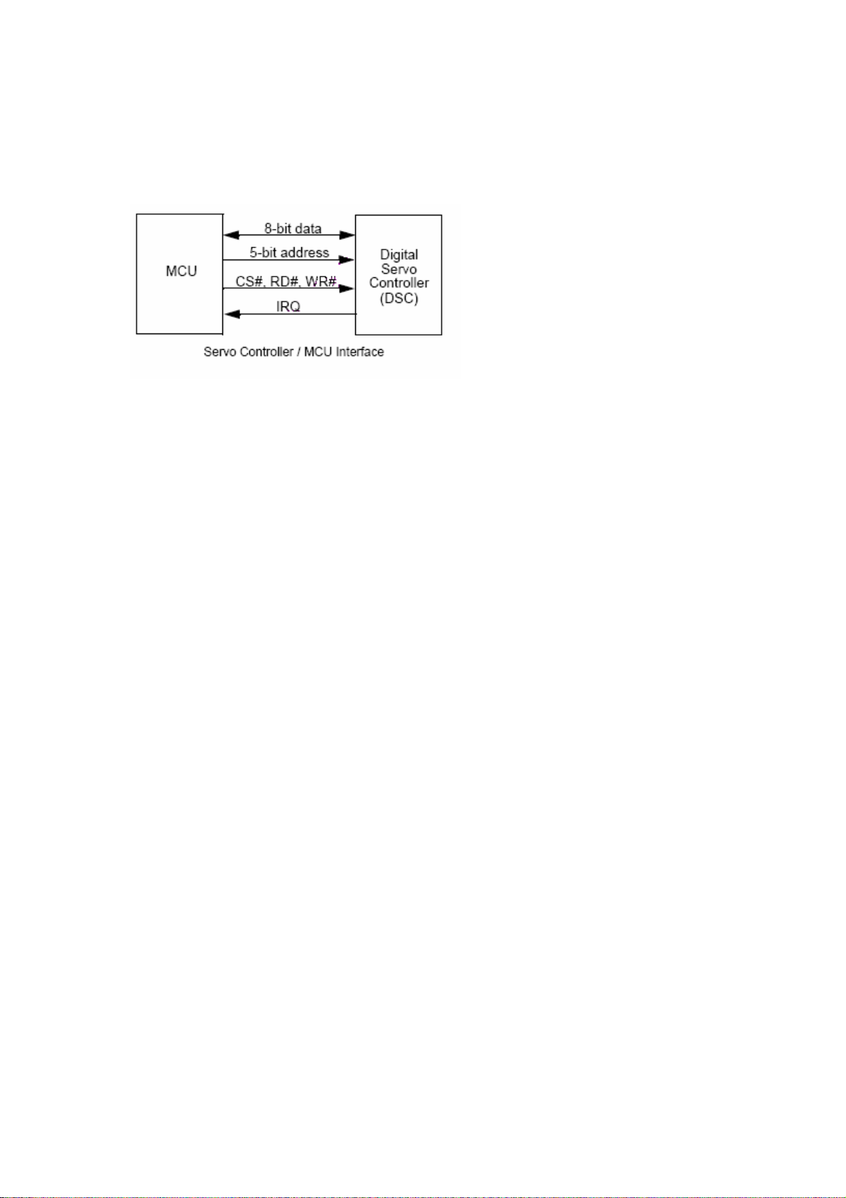
9 Digital Servo Controller
The digital servo includes an internal
DSP, on-chip RAM and ROM, control
logic, a loader interface, a serial
interface, and an on-chip ADC-DAC,
and interfaces with the MCU.
The MCU handles the high-level
functions of optical disk and front-end
system control. The interface between
the servo controller and the MCU is
illustrated in the Figure.
11 FRONT PANEL
VFD CONTROLLER
The VFD controller is a NEC uPD16311. This controller is not a processor, but does
include a simple state machine which scans the VFD and reads the front panel button matrix. The
16311 also includes RAM so it can store the current state of all the VFD icons and segments.
Therefore, the 16311 need only be accessed when the VFD status changes and when the button
status is read. The ES6808/ES6809 can control this chip directly using PIO pins or can allow the
front panel PIC to control the VFD.
12 RESET CIRCUITRY & VOLTAGE REGULATORS
Two different chips are supported to provide the power-on-reset DS1811 or AAT3520. (optional)
Voltage regulators:
U11: LM1117(1.8V) For 2V PLL power supply
U12: 7805 For 5V power supply
U13: LM1117(3.3V) For 3.3V power supply
10
Page 11

13 CONNECTORS
13.1 LOADER CONNECTORS:
11
Page 12

13.2 SCART CONNECTOR
Some cheaper SCART cables use unshielded wires, which is just about acceptable for
short cable lengths. For longer lengths, shielded co-ax cable become essential.
Scart Signals:
Audio signals
0.5V RMS, <1K output impedance, >10K input impedance.
Red, Green, Blue
0.7Vpp ?2dB, 75R input and output impedance. Note that the Red connection (pin 20) can
alternatively carry the S-VHS Chrominance signal, which is 0.3V.
Composite Video / CSync
1Vpp including sync, ?2dB, 75R input and output impedance.Bandwidth = 25Hz to 4.8MHz for
normal TV Video de-emphasis to CCIR 405.1 (625-line TV)
Fast Blanking
75R input and output impedance. This control voltage allows devices to over-ride the composite
video input with RGB inputs, for example when inserting closed caption text. It is called fast
because this can be done at the same speeds as other video signals, which is why it requires the
same 75R impedances.
12
Page 13

0 to 0.4V: TV is driven by the composite video input signal (pin 19).
Left unconnected, it is pulled to 0V by its 75R termination.
1V to 3V: the TV is driven by the signals Red, Green, Blue and composite sync. The
latter is sent to the TV on pin 19. This signal is useful when using a TV to display the
RGB output of devices such as home computers with TV-compatible frame rates. Tying
the signal to 5V via 100R forms a potential divider with the 75R termination, holding the
signal at around 2V. Alternatively, if a TTL level (0 to 5V) negative sync pulse is
available, this will be high during the display periods, so this can drive the blanking signal
via a suitable resistor.
Control Voltage
0 to 2V = TV, Normal.
5 to 8V = TV wide screen
9.5 to 12V = AV mode
14. CIRCUIT DESCRIPTION
14.1 POWER SUPPLY:
o Socket PL1 is the 220VAC input.
o 3.5A fuse F1 is used to protect the device against short circuit and
unexpected overloads.
o Line filter (L1) and a capacitor (C32) are used to block the parasitic
coming from the mains. They also prevent the noise, produced in the
circuit, from being injected to the line.
o Voltage is rectified by using D1-D4 diodes. Us ing capacitor C1,C2 (47?f)
a DC voltage is produced. (310- 320VDC).
o The current in the primary side of the transformer TR1 comes to the
SMPS IC (IC3 TOP248). The SMPS IC has a 6-pin package and an
internal MOSFET with a heat-sink is mounted on it. It has a built-in
oscillator, overcurrent and overvoltage protection circuitry and runs at
~30kHz. It starts with the current from the primary side of the transformer
and follows the current from the feedback winding.
o Feedback current is deteceted by optocoupler IC2. Depending on the
control current coming from the secondary side, SMPS IC keeps the
output voltage constant by controlling the duty cycle of the ~30kHz signal
(PWM) at the primary side of the transformer.
o Voltages on the secondary side are as follows: +24 Volts at D11, +12
Volts at D17, +5V at D20, +3.3V D32, -5V D24, -22 Volts at D25.
o Using the output of the D20, a photo diode inside of the IC2 generates
feedback signal bu using optocoupler's photo transistor. This photo
transistor adjusts the control voltage at the IC3 pin5. The voltage at this
pin effects the pwm output frequency on the IC3 pin6 (Drain pin). And
finally output voltages reach their correct values by this way.
13
Page 14

o Standby mode controlled by standby control transistor Q5. Standby control
signal comes from PL805 connector and generated by ES680X IC.
o –22 Volts is used to feed the VFD (Vacuum Fluorescent Display) driver IC
on the front panel.
14.2 FRONT PANEL:
o All the functions on the front panel are controlled by ES6808/09) on the
mainboard. Key scanning and IR checking operations on the standby mode
are controlled by VFD driver IC (uPD16311).
o ES60X8 IC sends the commands to uPD16311 via socket J1 (pins 2,3 and 4).
o There are 16 keys scanning function, 2 LED outputs, 1 Stand-by output and
VFD drivers on the uPD16311 IC.
o Front panel LED is bright red in stand-by mode and green when the device is
turned on.
o IR remote control receiver module (TSOP1836) sends the commands from
the remote control directly to the ES6808/09.
14.3 I/Os and Back Panel:
o After processing and amplification of audio signals amplificated audio signals
comes to back panel with this order:
o Front Right, Rear Right, Subwoofer, Center, Rear Left, Front Left
o There are 2 SCART connectors on the back panel. An input scart (P4) and an
output (TV) scart (P5)
o (Scart1 is for input on Scart mode and Scart2 is for TV output), 2 pieces RCA
audio jacks (L,R) for audio output, 1 RCA connector for CVBS out, 1 RCA
Connector for coaxial S/PDIF input, 1 digital optical ouput connector for
S/PDIF output.
o U15 Op-amp IC is for RCA and scart audio outputs. ES6808/09 IC generates
PWM downmixed audio outputs for the scart and RCA connectors.
o Radio L,R, Scart connector input L,R, TV scart L,R input (TV mode) are
selected as analog audio source of the system by U24 MUX IC (74HC4052).
This selected analog audio source comes to the U23 (LM833 op-amp IC) for
amplification. By using ADC U14 (PCM1803) L and R signals becomes digital
audio signal and comes to ES6808/09 for audio proccessing operations.
14
Page 15

14.4 A/V SWITCHING SIGNALS:
Video Switching:
AUX36 HIGH ESS Video
AUX36 LOW Scart Video (&scart copy)
Audio Switching:
___________________________________________________________
I TV Scart X FM/DAB I
I___________________________________________________________I
I AUX12 0 1 0 1 I
I___________________________________________________________I
I AUX13 0 0 1 1 I
I___________________________________________________________I
14.5 DDX Board (Class-D Amplifier):
? Chipset : 2xDDX-2052
? Architecture : Half-Bridge x 5 + Full-Bridge x 1
? Power Supply : + 24V unipolar supply @ 9A max., + 3.3V @ 0.1A typ.
? Audio Input Interface: PWM
? Output Interface: Speaker Level
? Speakers: 4 Ohm Satellites + 8 Ohm Subwoofer
? Output Power: 5 x 15 W + 25 W
? DDX Audio processor :ES6808/09.
15 DAB Module Board (AV2600 only):
DAB Module RS200 is
for FM and DAB (Digital
Audio Broadcasting)
receiption.
The RS200 dual-band
module implements the core
functions of both a DAB Band
III and an FM radio receiver,
and is based on the DRE200
DAB base-band digital signal
processor. The RF circuitry
uses a down- converter
/synthesizer chipset from a
15
Page 16

TV tuner for lowest cost, and supports both FM and DAB signal reception via a
single antenna connection. FM signals are down-converted and digitised in the
same manner as DAB signals, and additional software running on the DRE200
DSP is used to perform FM demodulation.
16
Page 17

CD Update Procedure of AV2500D
1. Download the update file from the convenient link according to your default language choice.
2. While there is no CD in the DVD (No Disc Mode) , press “Menu 1 3 5 7” buttons on the remote control in order to
reach the Service Menu of DVD Player:
2.1. Note the software version described as “b.xx “ to be able to compare the sw. Version after update process.
3. Copy the update file to the desktop and rename it according to the update file name in the hidden menu of the device.
For example If C2M1AS__ is written then rename it like C2M1AS__.rom
If P6M1AS__ is written then rename it like P6M1AS__.rom
(If you receive the update file already renamed (with addition of .rom) from the customer technical support department
by giving the SAP code of the product then burn the already renamed file with nero program as it is shown below.)
4. Burn the renamed files by Nero program with below set up.
5. After burning process is completed, place the update CD into the DVD tray and press play button.
6. Wait to see the update process steps as shown below. When the sw. Update is completed unit will switch itself to
standby mode.
7. Finally, press the eject button and take out the update CD while DVD Player remains at stand by Mode.
8. Updating process has been completed. To check whether it is updated correctly or not, repeat the first step for
comparing software version
9. If the previous and letter names are different, CD is update has completed successfully. If the name remains same than
go through the steps from the beginning.
IMPORTANT NOTE: If the AC source breaks down while the updating the unit (main board) will be totally out of
order. This kind of units/boards is out of Warranty.
Page 18

S D 1 1 R P 4 B . R O M
S: Sony KHM 310 D: w/ DivX
K: Sony KHM 313 _: w/o DivX
M: Samsung S75
EXAMPLES
Av2500D w/o drm, w/o pso, bank1, KST tuner, HT300 SD11__.rom
Av2500D w/o drm, w/o pso, bank1, KST tuner, HT400 SD11__4.rom
Av2600D w/o drm, w/o pso, bank1, DAB, HT400 SD11__4B.rom
Av2500D w/DRM, w/o pso, bank3, HT400 SD31R_4.rom
Av2500 w/o DivX, w pso, bank1, HT300 S_11_P.rom
Av2600 w/o DivX, w pso, bank1, HT400, S75 M_11_P4B.rom
Av2550D w/o drm w/o pso, bank2, HT400, S75 MD22__4.rom
OSD language
bank
1: Std power
2: High power
R: w/DRM P: w/ proscan 4: HT400 B: DAB (AV2600)
_: w/o DRM _: w/o proscan P: Panasonic tuner
NOT USED
FOR HT300
NOT USED FOR
KST TUNER
Page 19

Pay attention the left side. Select CD and CD_ROM (ISO) on the upper left side of screen
Select No Multisession
Page 20

Format is Mode 1
Leave the dates as it is
Page 21

Leave it as it is
Click the “New” on the upper right corner of the screen
Page 22

Select your file from file browser then you will see your file in the “Name” section on the right side and then copy the files
to under “Name” section on the left side.(this is just an example you will see your file name when you are doing this
process)
Click the “Burns the current compilation”
Page 23

Then you will see this screen and click the “Burn” on the right upper side of screen
You will see this screen and tray will open itself on computer ,then place the CD in CD-ROM
And it will start writing. At the end you will see “burn complited”
Page 24

VFD-DATA
VFD-CLK
VFD-CS
GND
BANK0
CS0#
RAS0#
CAS#
DQMX
FLASH_CS
A
L22
FB
L23 FB
A16
BYTE
GND
DQ15/A_1
DQ7
DQ14
DQ6
DQ13
DQ5
DQ12
DQ4
VCC
DQ11
DQ3
DQ10
DQ2
DQ9
DQ1
DQ8
DQ0
GND
Boot from flashProgram flash
A
VCC
R6
R2
4.7K
4.7K
R833 OHM
AUX7
R933 OHM
R1133 OHM
R26OPEN
R350
MMA1
MMA3
MMA4
MMA5
MMA6
MMA7 MB7
MMA8
MMA9
MMA10
DSCK#
CKE
CS0#
RAS0#
CAS#
WE#
DQMX
BANK0
BANK1
R733 OHM
U3
23
A0
24
A1
25
A2
26
A3
29
A4
30
A5
31
A6
32
A7
33
A8
34
A9
22
A10
35
A11
38
CLK
37
CKE
19
CS
18
RAS
17
CAS
16
WE
15
DQML
39
DQMH
20
BA0
21
BA1
36
NC
40
NC
4Mx16 SDRAM (9ns)
AUX35
AUX30
DQ10
DQ11
DQ12
DQ13
DQ14
DQ15
VCCQ
VCCQ
VCCQ
VCCQ
VSSQ
VSSQ
VSSQ
VSSQ
DQ0
DQ1
DQ2
DQ3
DQ4
DQ5
DQ6
DQ7
DQ8
DQ9
VCC
VCC
VCC
VSS
VSS
VSS
32/64MBIT SDRAM
VD33
LA0
LA17
48
47
46
LA0
45
LD7
44
43
LD6
42
41
LD5
40
39
LD4
38
37
36
LD3
35
34
LD2
33
32
31
30
LD0
29
LOE#
28
G
27
26
E
LA1
GND
LA1 LD1
LA2
LA3
LA4
LA5
LA6
LA7
LA8
LA9
LA10
LA11
LA12
LA13
LA14
LA15
LA16
LA17
LA18
LA19
LCS3#
LOE#
RESET#
WRLL#
4-PIN EXTENSION FOR ROM EMULATOR INTERFACE
AUX2
AUX6
AUX4
EM-MARIN
RESET IC
U1
1
S0
2
S1
3
S2
4 5
GND SDA
AT24C01A-10TC-2.7
VD33
MB0MMA0
2
MB1
4
MB2MMA2
5
MB3
7
MB4
8
MB5
10
MB6
11
13
MB8
42
MB9
44
MB10
45
MB11MMA11
47
MB12
48
MB13
50
MB14
51
MB15
53
1
14
27
3
9
43
49
6
12
46
52
28
41
54
GND
A0
A1
A2
A3
A4
A5
A6
A7
A8
A9
A10
A11
A12
A13
A14
A15
A16
VCC
A17
A18
A19
CE
GND
OE
RESETCLK/CE1
WE ADDR/CE1
U7
D0
D1
D2
D3
D4
D5
D6
D7
12
11
10
9
8
7
6
5
27
26
23
25
4
28
29
3
2
30
31
1
22
24
Emulator socket(27C040/080-90)
U8
1 2
3 4
ROM EMULATOR SOCKET
8
_VCC
7
WC
6
SCL
VD33
AUX0
AUX3(6)
RESET#
AUX1
DMA4
DMA5
DMA6
DMA7
GND
VD33
DMA8
DMA9
DMA3
DMA2
DMA1
DMA0
DMA10
GND
VD33
DMA11
DBANK1
DBANK0
DSS0#
DRAS0#
GND
VDD2V
DCAS#
DCKE
DWE#
DSCK
DQM
DB7
GND
VD33
DB6
DB5
DB4
DB3
DB2
DB1
DB0
GND
VD33
DB8
DB9
DB10
DB11
DB12
DB13
GND
LD0
13
14
LD2
15
LD3
17
LD4
18
LD5
19
LD6
20
LD7
21
VD33
32
16
GND
LA20
LA21
VFD-DATA
VFD
J1
1
2
3
4
5
6
7
8
4 4
DMA8
DMA9
DMA3
DMA2
DMA4
DMA5
DMA6
DMA7 MMA7
DMA1
DMA0
DMA11
DBANK0
3 3
DSS0#
DRAS0#
DCAS#
R24 OPEN(4.7K)
VD33
RN10 33 OHM X 4
DCKE CKE
4 5
DWE# WE#
3
DSCK DSCK#
2
DQM
1
R27 33 OHM
DB1
DB3 MB3
DB7 MB7
DB8 MB8
DB11 MB11
DB13 MB13
DB15 MB15
2 2
LA16
LA15
LA14
LA13
LA12
LA11
LA10
LA9
LA20
LA21
WRLL#
RESET#
LA19
LA18
LA8 LD1
LA7
LA6
LA5
LA4
LA3
LCS2#
LA2
1
2
3
JP1 JUMPER
1 1
LCS3#
9
10
CON10
RN4 10 OHM X 4
4 5
3
2
1
RN6 10 OHM X 4
4 5
3
2
1
RN8 10 OHM X 4
4 5
3
2
1
RN9 10 OHM X 4
4 5
3
2
1
MMA8
MMA9
6
MMA3
7
MMA2
8
MMA4
MMA5
6
MMA6
7
8
MMA1
MMA0
6
MMA10DMA10
7
MMA11
8
6
7
8
6
7
8
BANK1DBANK1
MB0DB0
MB1
MB2DB2
MB4DB4
MB5DB5
MB6DB6
MB9DB9
MB10DB10
MB12DB12
MB14DB14
U6
1
A15
2
A14
3
A13
4
A12
5
A11
6
A10
7
A9
8
A8
9
NC
10
NC
11
W
12
RP
13
VPP
14
DU/WP
15
NC
16
NC
17
A17
18
A7
19
A6
20
A5
21
A4
22
A3
23
A2
24 25
A1 A0
29LV800BE-90
LJP1 for debug ;RL1 for production.
1-2
JP1 2-3
VD33
GNDGND
B
VCC33
R1 100K
Y1 27M
C3
C4
27PF
27PF
GNDGND
R12
GND
33 OHM
C10
OPEN
(15PF)
R17 4.7K
R18 4.7K
AUX1 PLL2
AUX0
U2
1
VD33
2
AUX[0]
3
AUX[3]
4
RESET#
5
AUX[1]
6
DMA[4]
7
DMA[5]
8
DMA[6]
9
DMA[7]
10
VSS
11
VD33
12
DMA[8]
13
DMA[9]
14
DMA[3]
15
DMA[2]
16
DMA[1]
17
DMA[0]
18
DMA[10]
19
VSS
20
VD33
21
DMA[11]
22
DRAS2#
23
DRAS1#
24
DCS1#
25
DCS0#
26
DRAS0#
27
VSS
28
VDD
29
DCAS#
30
DOE#
31
DWE#
32
DSCK
33
DQM
34
DB[7]
35
VSS
36
VD33
37
DB[6]
38
DB[5]
39
DB[4]
40
DB[3]
41
DB[2]
42
DB[1]
43
DB[0]
44
VSS
45
VD33
46
DB[8]
47
DB[9]
48
DB[10]
49
DB[11]
50
DB[12]
51
DB[13]
52
VSS
B
GND
AUX2
AUX6
AUX4
GND
AUX5
VDD2V
AUX32
AUX33
AUX31
AUX34
GND
198
199
200
201
202
203
204
205
206
207
208
AUX[6]
AUX[2]
AUX[5]
AUX[4]
FLAG[2]/AUX32
VSS
VDD
FLAG[3]/AUX33
FLAG[4]/AUX34
FLAG[1]/AUX31
VSS
ES680XFA
VD33
DB[14]
DB[15]
LA[16]
LA[15]
LA[14]
LA[13]
LA[12]
LA[11]
VSS
VD33
5354555657585960616263646566676869707172737475767778798081828384858687888990919293949596979899
LA15
LA14
LA12
LA11
LA16
DB14
DB15
LA13
VDD2V
C46
0.1UF
VD33PLL
C53
10UF
VD33
GND
C26
0.1UF
VD33
VD33
VD33
197
LA10
GND
196
VD33
LA[10]
LA9
0.1UF
XOUT
CPUCLK
194
195
CLK
VSS
LA[9]
LA[20]
LA21
LA20
C47
0.1UF
C54
0.1UF
XIN
AUX17
AUX16
191
192
193
VID_XI
VID_XO
HSYNC/AUX16
LA[21]
LWRLL#
LA[19]
LA18
WRLL#
LA19
GND
C27
0.1UF
VSYNC/AUX17
LA[18]
L1 FB
L20
3.3UH
VDD2V
C5
L2 FB
1000PF
VCC33
VD33
R263
0
C36
GND
EAUX02
EAUX03
EAUX01
EAUX00
AUX37
AUX36
GND
182
183
184
185
186
187
188
189
190
VSS
VD33
AUX[7]
EAUX01
EAUX00
EAUX03
EAUX02
FLAG[6]/AUX36
FLAG[7]/AUX37/CAMIN7
LA[8]
VSS
VDD
LA[7]
LA[6]
LA[5]
LA[4]
LA[3]
VSS
LA8
LA4
LA6
LA3
LA5
LA7
VDD2V
L3FB
GND
VD33
C49
0.1UF
VCC33
L4 FB
GND
C48
0.1UF
OSC, RESET, TTL, PLL
C28
C29
0.1UF
0.1UF
R264
OPEN
180
181
MDET
VD33
LA2
0.1UF
179
OPEN
OPENSW
LA[2]
LA[17]
LA17
AGND
C6
GND
HOMESW
177
178
CLOSE
HOMESW
LA[0]
LCS0#
LA0
AVD33
C1
0.1UF
DVCC
C7
10UF
175
176
FGIN
CLOSESW
LCS1#
LCS2#
LCS2#
C50
0.1UF
GNDV
C30
0.1UF
AGND
AUX7
MDET (3)
OPEN (3)
OPENSW (3)
CLOSE (3)
HOMESW (3)
CLOSESW (3)
AMPSTBY (3)
AGND
DVCC
170
171
172
173
174
IP1
DVCC
IDSEL
AMPSTBY
VSS
VDD
LCS3#
LD[7]
LCS3#
GND
LD6
LD7
VDD2V
C51
10UF
GND
C55
10UF
AVD33
169
AVSS
LD[6]
LD5
C31
0.1UF
C
C2
10UF
167
168
IN
INB
AVDD3
LD[5]
LD[4]
LD[3]
LD4
LD3
VD33DAC
C56
0.1UF
C
REFD
166
REFD
LD[2]
LD2
VDD2V
VDD2V
VD33
R10
4.7K
REFD
C8
10UF
AGND
R40 4.7K
TRO
DMO
FOO
SLO
160
161
162
163
164
165
SLO
TRO
FOO
TEBC
RPBC
TESTDA
FLAG[0]/AUX30/CAMIN0
FLAG[5]/AUX35/CAMIN5
RXD0/AUX14/PWM_O4R
TXD0/AUX15/PWM_O4L
TBCK/PWM_O1R
TSD3/PWM_O3R
TSD2/PWM_O3L
TSD1/PWM_O2R/PLL1
TSD0/PWM_O2L/PLL0
TWS/PWM_O1L/PLL2
VSS
VD33
LD[1]
LD[0]
LOE#
LA[1]
100
101
LA1
PLL3
LD1
LD0
LOE#
VD33
GND
C39
0.1UF
GND
VD33
C9
0.1UF
IN (4)
INB (4)
TEBC (4)
TRO (4)
HOMESW
SLO (4)
FOO (4)
DMO (4)
AGND
ES680X
157
158
159
SLV
DMO
AVSS
AVDD3
VREFIN
VREFOUT
RFENV
CE
BSUM
LDON
MIRR
DFCT
SCLK
SDATA
SDEN
IP2
LDCO
VSS
VDD
VSS
RXD1/AUX12
TXD1/AUX13
VD33
MCLK
VSS
VD33
ADC_CAP
MIC
ADC_BIAS
UDAC
CDAC
YDAC
VS33DAC
VD33DAC
VDAC
FDAC
RSET
COMP
VREF
VS33PLL
SPD_DOBM/PLL3
SPDIF
VD33PLL
102
103
104
VD33PLL
SPDIF_IN (7)
SPDIF_OUT (7)
C32
10UF
VD33
PLL3
TE
FE
LG
RX
TX
0
VD33
GND
156
155
154
153
152
151
150
149
148
147
146
145
144
143
142
141
140
139
138
137
136
135
134
133
132
131
130
129
128
127
126
125
124
123
122
121
120
119
118
117
116
115
114
113
112
111
110
109
108
107
106
105
GND
GND
CLK SOURCE
CRYSTAL OSC
DCLK INPUT1
PLL0
PLL1
PLL3
C11
0.1UF
AVD33
VREFOUT
RFENV (4)
TE
TE (4)
CE (4)
FE
FE (4)
BSUM
BSUM (4)
LDONJ (4)
MIRR (4)
DFCT (4)
SCLK (4)
SDATA (4)
SDEN (4)
CD_DVDCT (3)
GND
AUX30
AUX35
VDD2V
GND
RXD1
TXD1
VD33
MCLK
PWM_04R
PWM_04L
PWM_01R
PWM_03R
PWM_03L
GNDA
VCC33A
PLL1 PWM_02R
PLL0 PWM_02L
PWM_01L
PLL2
R28 33
R29 33
R30 33
UDAC
CDAC
YDAC
GNDV
VD33DAC
VDAC
RSET
COMP
VREF
GND
C16 0.1UF
AAT3521 SOT-23(5pin)
AAT3520 SOT-23(3pin)
C17
0.1UF
VCC33VCC33VCC33
R4
R3
R5
4.7K
OPEN
4.7K
HOMESW
OPENSW
CLOSESW
VD33 VD33 VD33
GND GND
R34 360 OHM 1%
GNDVGNDV
U4
RESET
GND
NC
EN
VCC
U5
GND
RESET
VCC
R13
4.7K(OPEN)
R19
4.7K
VCC33A
VCC33A
GNDA
1
2
3
4
5
1
2
3
C18
0.1UF
VD33
R14
4.7K(OPEN)
R20
4.7K
R23 39K
C12
C13
0.1uF
1uF
GNDGND
R25
4.7K
GNDA GNDA
ADCLRCK (5)
ADCBCK (5)
ADCDOUT (5)
UDAC (6)
CDAC (6)
YDAC (6)
VDAC (6)
C14
0.1UF
VCC
GND
C19
0.1UF
C33
0.1UF
HOMESW (3)
OPENSW (3)
CLOSESW (3)
4.7K
MIRR
C15
0.1UF
R31 100K
RESET#
ES6620
C20
0.1UF
C34
10UF
R15
4.7K(open)
R21
SVREF (3,4)
D
EAUX00
AUX5
RXD1
TXD1
AUX16
AUX17
AUX31
AUX32
AUX33
AUX34
AUX36
AUX37
EAUX01
EAUX03
MCLK
VD33
D
GNDGND
C21
0.1UF
C35
0.1UF
R16
4.7K(OPEN)
R22
4.7K
RDS_DATA (7)
RDS_CLK (7)
AUX12 (5)
AUX13 (5)
AUX16 (7)
AUX17 (7)
AUX31 (7)
AUX32 (7)
AUX33 (7)
AUX34 (7)
AUX36 (5)
AUX37 (4)
EAUX01 (7)
EAUX03 (8)
MCLK (5)
LD0
LD1
LD2
LD3
LD4
LD5
LD6
LD7
LCS2#
GND
C22
0.1UF
HYPERSTREAM
PWM_01L
PWM_01R
PWM_02L
PWM_02R
PWM_03L
PWM_03R
PWM_04L
PWM_04R
PLL1PLL2
0
0
011
0
0
1
0
1
0 0
1
0
1
1
1
AUX32(7)
AUX31(7)
EAUX01(7)
EAUX02
U17
3
D0
Q0
4
D1
Q1
7
D2
Q2
8
D3
Q3
13
D4
Q4
14
D5
Q5
17
D6
Q6
18
D7
Q7
1
OC
11
CLK
74HCT374
C23
C24
0.1UF
0.1UF
C38
C37
0.1UF
0.1UF
PLL0
2
5
6
9
12
15
16
19
0
0
1
1
0
11
AUX32
AUX33
AUX31
AUX34
AUX16
AUX17
EAUX02
EAUX03
EAUX00
AUX36
EAUX01
AUX37
AUX30
AUX35
RXD1
TXD1
PWM_01R
AUX7
GND
PWM1L (6)
PWM1R (6)
PWM2L (6,8)
PWM2R (6)
PWM3L (6)
PWM3R (6)
PWM4L (6)
PWM4R (6)
MULT
S-CHIP
4.5X
5.0X
BYPASS
4.0X
4.25X
4.75X
5.5X
6.0X
1
2
3
4 5
RN1 4.7K X 4
R271 4.7K
R268 4.7K
R269 4.7K
R270 4.7K
1
2
3
4 5
RN3 4.7K X 4
1
2
3
4 5
RN5 4.7K X 4
R265 4.7K
R267 4.7K
FBL_AUX2 (7)
12V_DET (7)
ST_LED (7)
TU_LED (6)
8
7
6
8
7
6
C25
0.1UF
E
FREQUENCY
S-CHIP
121.5
135
N/A
108
114.75
128.25
148.5
162
VD33
8
7
6
8
7
6
8
7
6
RN11 33 X 4
1
FAST_BLK (7)
2
PIN8 (7)
3
CONT_VOL (7)
45
Pin8_bypass (7)
1
2
SWITCH_SCART_AUDIO (6)
3
TUNER_MUTE (7)
45
RN12 33 X 4
POWER_SWITCH (8)
VESTELKOM
Title
ES68xx, MEMORY
Size Document Number Rev
VESTEL-AV2500D
Date: Sheet of
E
2 8Friday, October 14, 2005
A8
Page 25

A
B
C
D
E
KHM310
24PIN
(N.C)
HFM
MD
CD-LD
VR-CD
(N.C.)
Vcc
6
5
4
3
2
1
E
Vc
F
B
A
RF
D
C
TT+
F+
F-
TP1
TP2
TP3
TP4
TP5
TP6
TP7
TP8
TP9
TP10
24
23
22
21
20
19
18
17
16
15
14
13
12
11
10
9
8
7
6
5
4
3
2
1
MGND
SLED+
SLEDHOMESW
MGND
RFGND
MDI
LDO1
F
B
A
PVC
CD_DVD
C
TRACKFOCUS-
LOADLOAD+
SPINSPIN+
LDO2
MDI
LDO1
VR_DVD
VR_CD
E
PVC
F
B
A
RF
CD_DVD
D
C
TRACK+
TRACKFOCUS+
FOCUS-
LDO2
VR_DVD
VR_CD
E
RFVCC
RFPVC
D
FOCUS+
RFGND
MDI (4)
E (4)
F (4)
B (4)
A (4)
RF (4)
D (4)
C (4)
TP11
TP12
TP13
TP14
TP15
TP16
TP17
TP18
TP19
TP20
CLOSESW (2)
OPENSW (2)
HOMESW (2)
RFVCC
RFGND
LDO2
VD_DVD
VR_CD
E
RFVCC
RF
D
TRACK+
FOCUS+
RFGND
PVC (4)
C62
0.1UF
C59
100UF
RFGND
FOCUS(4)
SLED(4)
MVCC
C60
0.1UF
OPEN(2)
CLOSE(2)
LOADLOAD+
SLEDSLED+
FOCUSFOCUS+
100UF/12V
R46 2.7K
R50 20K
OPEN
CLOSE
GND-LD
DVD-LD
4 4
3 3
2 2
VR-DVD
GND-PD
CD/DVD
CN1
MDI
LDO1
F
B
A
CD_DVD
C TRACK+
TRACKFOCUS-
J3
1
2
3
4
5
CON5
J4
6
5
4
3
2
1
6pin/2.0MM
C63
RFVCC
RFGND
LDO2
RFVCC
RFGND
LDO1
1
2
3
4
5
6
7
8
9
10
11
12
13
14
10uH
C57
0.1U
C64
0.1U
U9
AM5868S
VINFC
OP2INOP2IN+
VINSL
OP2OUT
FWD
REV
VCC1
VOTRVOTR+
VOSLVOSL+
VOFCVOFC+
L5
R36 15
2SB1132R
L6
10uH
L7
10uH R43
2SB1132R
L8
10uH
GND
GND
29
30
MGND
Q2
15
Q5
MUTE
BIAS
VINTK
OP1IN+
OP1IN-
VINLD
GND
VCTL
OP1OUT
VCC2
VOLD-
VOLD+
VOTK-
VOTK+
C58
100UF/10V
32
1
C61
1000PF
32
1
C66
1000PF R42
MVCC
28
27
26
25
24
23
22
21
20
19
18
17
16
15
R38 1K
1
D1
IN4148
C65
100UF/10V
R44 1K
1
D2
IN4148
R45
33K
R47
22K
VC2
R49 39K
OP1IN+
OP1IN-
R52 3K
MGND
MVCC
OP1OUT
SPIN-
SPIN+
TRACKTRACK+
RFGND
RFGND
CDLDO (4)
DVDLDO (4)
TRACKING (4)
SPINDLE (4)
MGND
D3IN4148
1
R48 33
C68
0.1U
CD_DVDCT(2)
AMPSTBY (2)
SVREF (2,4)
RFVCC
R37
10K
R39
10K
2
1 3
SPIN+
SPIN-
R53
10K
R56
1.5K
R58
22K
MGND MGND
Q3
2N3904
R41
100K
CD_DVD
18K
2
R51
10K
R54
1.5K
R59
22K
2 1
RFVCC
RFGNDRFGND
TOP
Q6
2N3904
1 3
2SK3018
2SK3018
OP1IN+
OP1IN-
R96
100
R99
100
VR_CD
VR_DVD
R55
4.7K
RFGND
RFGND
MVCC
1
D4
IN4148
1
IN4148
D5
MDET (2)
OP1OUT
Q1
31
2
RFGND
Q4
31
2
RFGND
TOP
12
R57
1M
C75
1U
RFGND
VCC33
1 2
L11
Bead
C76
1U
RF33V
C77
10UF/16V
C
VESTELKOM
Title
OPU, MOTOR, POWER
Size Document Number Rev
VESTEL-AV2500D
D
Date: Sheet of
E
3 8Friday, October 14, 2005
A8
MVCC
1 1
VCC
1 2
L9
Bead
33UF/16V
C69
+
MGND
A
MGND
C71
0.1
VCC RFVCC
1 2
C72
0.1U
GND
L10
Bead
C73
1U
RFGND RFGND
B
C74
10UF/16V
RFGND
Page 26

5
DIN
DIP
C80
RFVCC
C67
0.1U
D D
RF(3)
RFGND
D(3)
C(3)
B(3)
A(3)
C C
B B
HEADER 10
A A
CON4
F(3)
E(3)
PVC(3)
P1
1
2
3
4
5
6
7
8
9
10
VCC_AMP_3V3
J5
1
2
3
4
GND
C105
0.1U
GND
RFGND
C88
680PF
C93
680PF
C97 680PF
C98 680PF
C99 680PF
C100 680PF
C101
100P
RFVCC
RFGND
VC25
C112
47U/16V
RFGND
C117
220uF/16V
+3V3
VCC
C145
220uF/16V
VCC_AMP_24V
1
DVDFRP
2
DVDRFN
3
A2
4
B2
5
C2
6
D2
7
CP
8
CN
9
D
10
C
11
B
12
A
13
NC(CD_D)
14
NC(CD_C)
15
NC(CD_B)
16
NC(CD_A)
MDI(3)
GND
DVDLDO
CDLDO
MDI
+5VST
C118
0.1uF
L15
22U
AUX37 (2)
-5V
C146
0.1uF
L12
22U
L14
22U
DVDLDO(3)
CDLDO(3)
GND
5
0.1U(0.01U)
C82
0.1U(0.01U)
RFVCC
646362616059585756555453525150
AIP
AIN
ATOP
ATON
RFSIN
NC(RFDC)
ES6602
CD_F
CD_E
VPBVCDVDLD
CDLD
171819202122232425262728293031
0(15k)
R33
R32
OPEN(75k)
RFGND
C121
100uF/16V
GND
C132
100uF/16V
GND
C135
220uF/16V
GND
C137
100uF/16V
GND
VPA
RFAC
DVDPD
CDPD
RFGND
C122
0.1uF
C133
0.1uF
C136
0.1uF
C138
0.1uF
BYP
VNB
DIN
LDON
C81
0.1U
C83
0.1U
DIP
FNP
FNN
VNA
MMON(LINK)
MIRRMPMB
MLPF
R79
VCC33
VCC5
TUNER_+12V
12VST
49
RX
NC(MEV)
MIN
PIO(MEVO)
32
MEVO
MIN
-5V
4
C78
0.1U(0.033U)
C79
0.1U(0.033U)
V33
FE
TE
PI
DFT
LDONJ
L16
22uH
U10
48
47
46
45
44
43
42
41
40
39
38
37
36
35
34
33
C107
0.22U
RFVCC
C109
8200P
4
RFVCC
RF33V
RFGND
100uF/16V
C87
1000P
R66 12K(1%)
SDEN
SDATA
SCLK
NC(LCP)
NC(LCN)
MNTR
NC(CE)
NC(V25)
V125
DB(TPH)
C108
150P
C110
8200P
4.7K
C140
C94
0.1U
SVREF
C102
0.1U
C103
OPEN
RFGND
MIRRO
LDONJ (2)
RFVCC
RFGND
RFGND
RFVCC
DFCT
GND
R60
4.7K
ASI
C113
OPEN
C141
0.1uF
RFGND
FEI
TEI
RFGND
VD33
VCC-5
R61
4.7K
RFGND
C89 33P
C95 33P
C96 33P
R71 33
R72 33
R73 33
SVREF (2,3)
MIRR (2)
U11
REG1117-ADJ
GND
+5VST
C139
0.1UF
GND
RFGND
VOUTVIN
TAB
ADJ
1
C134
10uF/16V
4
TOP
1 2
SOT-223
INB (2)
IN (2)
SDEN (2)
SDATA (2)
SCLK (2)
DFCT(2)
23
4
U13
REG1117-3.3V
3
R81
412 OHM 1%
R82
249 ohm 1%
GND
VOUTVIN
ADJ
1
GND
DFCT
C147
OPEN
3
SLO(2)
FOO(2)
R77
5.1K
Q8
8050
RFGND
23
R83
OPEN
2
R74
5.1K
R67
GND
C84
1K
C90
0.01
RFVCC
1 3
VCC33
C114
0.1UF
GND
VD33
GND GND
0.47UF
RFGND
2
Q7
2SK3018
2SK3018
Q9
2
R78 0
C126
100UF
C142
100UF
1.2K
R62
0 OHM
R63
R70
0 OHM
TEBC
GNDA
R75
0(OPEN)
C115
100UF
31
3 1
(2.0V)
VDD2V
C127
0.1UF
GND
(STBY 3.3V)
C143
0.1UF
RFENV (2)
SLED (3)
CE (2)
TEI
R76
3.3K
TEBC (2)
VCC33A
GNDA
1000PF
RFGND
C116
0.1UF
TUNER_+12V
GND
TE
C104
ASI
FEI
C128
100UF
2
R64
R68
TE (2)
0
C85
330PF
RFGND
OPEN
FE
C91
OPEN
Q16
2SK3018
Q17
2SK3018
AGND
GNDA
U12
1 3
7805
V1N VOUT
GND
2
AGND
BSUM (2)
FE (2)
2
2
GND
GND
31
3 1
C129
100UF
SVREF
TRO(2)
DMO(2)
FEI
MGND
RFGND
GNDV
R65
R69
R80
3.3K
SVREF(2)
GNDA
RFGND
C130
0.1UF
1K
C86
1.2K
C92
C40
1000PF
GNDA
1
TRACKING (3)
0.01
RFGND
SPINDLE (3)FOCUS (3)
0.47UF
RFGNDRFGNDRFGND
FE (2)
VA5
C131
100UF
VESTELKOM
R84
0
GND
3
2
Title
RF-AMP
Size Document Number Rev
VESTEL-AV2500D
Date: Sheet of
1
4 8Friday, October 14, 2005
A8
Page 27

5
4
3
2
1
L25
D D
U25
CDAC_O_OUT
RED_Y_AUX2(7)
YDAC_O_OUT
GREEN_OUT(7)
GREEN_Cr_AUX2(7)
UDAC_OUT(6)
R85
0
CDAC_OUT(6)
R86
0
VDAC_OUT(6)
R87
0
YDAC_OUT(6)
C C
R89
0
UDAC_O_OUT
CDAC_O_OUT
DVD_CVBS_OUT
R88
75
YDAC_O_OUT
VCR_VID (7)
VCC-5
L24
22U
1
BY_IN_OUT1
2
BX_IN_OUT
3
CY_IN_OUT
4
CX_CY_IN_OUT
5
CX_IN_OUT
6
INH
7
VEE
8 9
GND C
M74HC4053
GND
VCC
BX-BY_OUT_IN
AX-AY_OUT_IN
AY_IN_OUT
AX_IN_OUT
16
15
14
13
12
11
A
10
B
TV_AUDIO_IN_R(7)
LINE_INT_R
C154 10u/50V
TUNER_IN_R(7)
SCART_AUDIO_IN_R_AUX2(7)
VCC-5
R98 4k7
R102
47K
L27
GND GND
R103
2K2
22U
C148
100n/25V
BLUE_OUT (7)
UDAC_O_OUT
AUX36 (2)
U24
1
Y0
2
Y2
3
COM_Y_OUT_IN
4
Y3
COM_X-OUT_IN
5
Y1
6
INH
7
VEE
8 9
GND B
M74HC4052
GND
VCC
X2
X1
X0
X3
U26
LINE_OUT_L_M(6,7)
SCART_AUDIO_IN_L_AUX2(7)RED_OUT (7)
LINE_OUT_R_M(6,7)
SCART_AUDIO_OUT_R(7)
SCART_AUDIO_IN_R_AUX2(7)
1
BY_IN_OUT1
2
BX_IN_OUT
3
CY_IN_OUT
4
CX_CY_IN_OUT
5
CX_IN_OUT
6
INH
7
VEE
8 9
GND C
BX-BY_OUT_IN
AX-AY_OUT_IN
AY_IN_OUT
AX_IN_OUT
VCC
16
15
14
13
12
11
A
10
B
M74HC4053
GND
L26
+5VST
22U
C156
16
15
14
13
12
11
10
A
100n/25V
GND
AUX12 (2)
C15510u/50V
LINE_INT_L
R104
47K
R94 4k7
R105
2K2
SCART_AUDIO_IN_L_AUX2 (7)
TV_AUDIO_IN_L (7)
TUNER_IN_L (7)
AUX13 (2)
GND
GND
22U
C149
100n/25V
SCART_AUDIO_OUT_L (7)
CVBS_OUT (7)
DVD_CVBS_OUT
CVBS_IN_AUX2 (7)BLUE_Cb_AUX2 (7)
AUX36 (2)
+5VST
GNDGND
SWITCH_SCART_AUDIO (2)
L18
B B
LINE_INT_R
VCC-5
C159
R107 8K2
R106 10k
R108 200
L19
470p/50V
22U
C162
10u/50V R121 4.7K(OPEN)
GND
C163
100n/16V
GND
GND
1
OUT1
2
INV_IN1
3
NONINV_IN1
4 5
VCC- NONINV_IN2
C164
10u/50V
U23
LM833
VCC+
OUT2
INV-IN2
8
7
6
GND
C157
100n/16V
GND
C161
470p/50V
R116 200
C158
10u/50V
GND
R110 10K
R117 8K2
22U
C160 10u/50V
VCC5
LINE_INT_L
R109 150
R111 150
C165
0.1UF
C166
4.7UF
VCC33A
VREF1
C168
4.7UF
GNDA GNDA GNDAGNDA
A A
TI 2-CHANNEL AUDIOADC
U14
VA5
5
VCC
14
VDD
2
VINR
1
VINL
3
VREF1
4
VREF2
13
DGND
6
AGND
PCM1802
SCKI
BCK
LRCK
DOUT
FSYNC
PDWN
OSR
BYPAS
FMT0
FMT1
MODE0
MODE1
15
11
10
12
9
7
16
8
17
18
19
20
GNDA
ADCBCK
ADCLRCK
ADCDOUT
VCC33A
R112 4.7K
R118 4.7K(OPEN)
MCLK (2)
ADCBCK (2)
ADCLRCK (2)
ADCDOUT (2)
R113 4.7K(OPEN)
R119 4.7K
R114 4.7K(OPEN)
R115 4.7K
R120 4.7K
GNDA GNDA
VESTELKOM
Title
AUDIO & VIDEO MUX
Size Document Number Rev
VESTEL-AV2500D
5
4
3
2
Date: Sheet of
1
5 8Friday, October 14, 2005
A8
Page 28

A
B
C
D
E
C43
4 4
VCC5
3
GNDA
U19A
PWM4L(2)
3 3
PWM1L(2)
PWM4R(2)
PWM1R(2)
2 2
PWM2L(2,8)
1 2
74HCT04
U19B
3 4
74HCT04
U16F
13 12
74HCT04
U16E
11 10
74HCT04
U19F
13 12
74HCT04
1
FL
1
FR
R124 3.3K
GNDA
FL (8)
R133 3.3K
GNDA
FR (8)
C171 100UF
C173
2.2nF
C183 100UF
C185
2.2nF
R125 4.7K
1
R134 4.7K
1
R126 1.8K
C174
6.8nF
GNDA
R135 1.8K
C186
6.8nF
GNDA
1
1
GNDA
1
1
2
C172 220PF
R127 10K
5
6
C184 220PF
R136 10K
VCC-5
VCC5
VCC-5
U15-1
84
LM833D
V+
V-
84
V+
V-
1
U15-2
LM833D
7
C169
10UF
QUIET0
C178
10UF
GNDA
QUIET0
1
1
R122
1
470 OHM
R123
100K
R128
1
470
R130
1
470 OHM
R131
100K
R137
1
470
GNDAGNDA
GNDA
C170
22PF
2
C179
22PF
2
GNDA
GNDA
LINE_OUT_L_M (5,7)
Q14
9014
1 3
LINE_OUT_R_M (5,7)
Q15
9014
1 3
UDAC(2)
CDAC(2)
YDAC(2)
VDAC(2)
R272
47
AGND AGNDAGND AGND
1uF
1uF
1
R273
47
1
1
R274
47
C45
BEAD
L21
1
R275
47
C41
10uF/16V
C44
1uF
VCCV
C52
1uF
AGND AGND
VCCVVCC
1
2
3
4
5
6
7
C42
0.1uF
U18
IN1
IN2
IN3
VCC
IN4
IN5
NC
FMS6145
OUT1
OUT2
OUT3
VSS
OUT4
OUT5
NC
14
13
12
11
10
9
8
AGND
1
R90
75 (open)
R91
75(open)
AGND AGND GNDAGNDA
1
1
R92
75(open)
1
R93
75(open)
UDAC_OUT (5)
CDAC_OUT (5)
YDAC_OUT (5)
VDAC_OUT (5)
U16A
1 2
74HCT04
U16B
PWM2R(2)
PWM3L(2)
1 1
PWM3R(2)
3 4
74HCT04
U16C
5 6
74HCT04
U16D
9 8
74HCT04
A
SUB_D- (8)
SUB_D+ (2,8)
LS
LS (8)
CC
CC (8)
RS
RS (8)
VCC5
VCC-5
GNDA
C206
0.1UF
C211
0.1UF
GNDA
B
C207
0.1UF
C212
0.1UF
C208
10uF/16V
C213
10uF/16V
C209
10uF/16V
C214
10uF/16V
TUNER_+12V
D10
BAS70-04
1
C210
220uF/25V
GNDA
VCC5
AUX3(2)
R158 1K
1
C
1
R160
1K(OPEN)
R161
470
1
2
GNDA
3
1
Q20
2N3904
1 3
2
R159
1K
MUTE CIRCUIT
R156
6.8K
1
1
C205
R157
2.2K
1
VCC5
13
Q19
2
8550
1
Q18
2
8550
D11
IN4148
13
QUIET0
1
GNDA
D
470uF/25V
VESTELKOM
Title
DVD AUDIO, VIDEO
Size Document Number Rev
VESTEL-AV2500D
Date: Sheet of
E
6 8Friday, October 14, 2005
A8
Page 29

5
12VST
R163
680
13
Q21
BC858B
D D
GREEN_Cr_AUX2(5)
C C
RED_Y_AUX2(5)
12VST
B B
CONT_VOL(2)
CONN TRBLK 15
15
14
13
12
11
A A
10
R180
470
Q29
BC858B
R200
470
GND
R228
10K
TUNER_VCC
T1
R232
56K
R_CLK
15
R_DATA
14
X41
13
X43
12
X40
11
TUCS
10
9
9
8
8
T_12V
7
7
6
6
5
5
4
4
3
3
2
2
1
1
GND
R176 270
13
R196
270
C225
100n/25V
R213
1K
R214
820
Q37
BC858B
2
2
Q25
BC848B
1 3
R181
330
GND
12VST
R191
680
2
Q32
BC848B
1 3
R201
330
GND GND GND
1 3
2
R220
10K
Q43
BC848B
1 3
SCART SWITCHING CIRCUITRY - AV & 16:9,4:3 Switching
GND
R233
56K
L39
L40
L46
L45
L44
L43
L42 22U
5
BLUE_Cb_AUX2(5)
R166
47K
2
C215
100u/25V
C219 47p
R182 7K5
R178 75
GND GND
R193
47K
2
C223 47P
CVBS_IN_AUX2(5)
D12
IN4148
1
1 3
R217
10K
C124
0.1uF
R225
GND
PIN8(2)
GND
C221
100u/25V
R202 7K5
R215
1K
Q38
BC858B
2
R221
10K
10K
RDS_CLK (2)
RDS_DATA (2)
AUX17 (2)
AUX16 (2)
AUX34 (2)
AUX33 (2)
TUNER_+12V
TUNER_IN_L (5)
TUNER_IN_R (5)
TUNER_MUTE (2)
TU_LED (2)
ST_LED (2)
2
L13
22uH
C123
100uF/16V
GND
R206 75
GND
BC858B
R183
470
Q30
BC858B
BC848B
1 3
Q22
R203
470
D13
IN4148
1
CONT_VOL_OUT
Q40
CONN TRBLK 15
R164
680
13
2
Q26
BC848B
R177
270
R184
330
R192
680
13
2
Q33
BC848B
R197
270
R204
330
Q24
BC858B
Q27
BC848B
T3
15
15
14
14
13
13
12
12
11
11
10
10
9
9
8
8
7
7
6
6
5
5
4
4
3
3
2
2
1
1
DAB
GND
12VST
1 3
1 3
C224
47p/50V
GND
2
1 3
GND
VCC
L17
22uH
FMnDAB
IC_CLOCK
IC_DATA
PO-RESET
4
SCART_AUDIO_IN_R_AUX2(5)
SCART_AUDIO_IN_L_AUX2(5)
R165
47K
2
C220 47p
GND
2
13
R175
10K
R179 10K
2
4
C216
100u/25V
R185 7K5
R205 7K5
TUCS
X40
X43
X41
R186 75
GND
R194
47K
C222
100u/25V
GND
CONT_VOL_AUX2
R171
10K
TUNER_IN_R (5)
TUNER_IN_L (5)
R95
100R
10K
GND GND
CONT_VOL_AUX2
R208 75
R209 75
GND
SPDIF_IN(2)
Pin8_bypass (2)
SPDIF_OUT(2)
VCC33
R167
VCR_VID(5)
R207
10K
R168
GND
VCC5
10K
CONN TRBLK 15
2
R237
10M
C233
0.1UF
R198 10K
1 3
GND
U20A
7404
VCC
1
T8
13
12
11
10
9
8
7
6
5
4
3
2
1
KST tunerPanasonic tuner
LINE_OUT_L_M (5,6)
LINE_OUT_R_M (5,6)
P4
1
2
3
4
5
6
7
8
9
10
11
12
13
14
15
16
17
18
19
20
21
SCART_IN
FBL_AUX2 (2)
Q35
BC848B
SPDIF_IN OPTION
12
U20F
13 12
7404
1
R239 1M
R_DATA
13
R_CLK
12
GND
11
TUCS
10
X40
9
X43
8
X41
7
6
GND
5
4
T_12V
3
2
1
3
P5
1
2
3
4
5
6
7
8
9
10
11
12
13
14
15
16
17
18
19
20
21
SCART_OUT
U20B
7404
TUNER_IN_R (5)
TUNER_IN_L (5)
ST_LED (2)
TU_LED (2)
3
SCART_AUDIO_OUT_R (5)
SCART_AUDIO_OUT_L (5)
TV_AUDIO_IN_R (5)
TV_AUDIO_IN_L (5)
R173 10K
R174 10K
C217 1n/50V
BLUE_SCART_OUT
CONT_VOL_OUT
GREEN_SCART_OUT
RED_SCART_OUT
FAST_BLK_TV
SCART_CVBS_OUT
GND
T2
T7
34
R236
10K
GND GND
U20E
11 10
7404
C218 1n/50V
GND
T4
T5
T6
R23122K
U20C
56
7404
9 8
RED_SCART_OUT
GREEN_SCART_OUT
BLUE_SCART_OUT
GREEN_SCART_OUT
RED_SCART_OUT
MGNDGND
C226
0.1UF
R234
0R
U20D
7404
2
VCC5
1 3
R222
10K
FAST_BLK(2)
R219
0R
R223
GND
R229
0R
R230
GND
VCC
GND
C232
10nf
SPDIF_INput
R235
75
VCC
R238
1
68 OHM
Component Video Output Connector
( Y Pb Pr )
J2
1
2
3
4
5
CON5
2
Q39
BC858B
R224
2
R227
10K
R216
0R
OPEN
R226
0R
OPEN
SPDIF_INput
CVBS_RCA
LINE_OUT_R_M(5,6)
LINE_OUT_L_M(5,6)
L41
47UH
12
C234
0.1UF
SPDIF ouput optional comps.
R218
100
10K
2
GREEN_OUT (5)
RED_OUT (5)
FAST_BLK_TV
Q42
BC848B
1 3
GND
SCART_CVBS_OUT
BLUE_SCART_OUT
L33 Bead
L37 Bead
L35 Bead (0R)
L36 Bead
L38 Bead
L34 Bead
MOFT3C2
3
GND
2
VCC
1
VIN
P3
CONT_VOL_AUX2
R188
0R
R211
0R
C70
C106
680pF
680pF
SUB-_OUT(8)
SUB+_OUT(8)
CC-OUT(8)
C111
470pF
RS-OUT(8)
FR-OUT(8)
FL-OUT(8)
LS-OUT(8)
R169
10K
R212
GND
GND
R172
R190
C119
680pF
2K
OPEN
OPEN
GND
1
R170
1K
GND
R187 0R
R189 0R
R210
0R
2
P6 RCA CONN 4
1
2
3
4
5
6
POWER OUT JACK
1
2
3
4
5
6
7
8
9
10
11
12
VCC5
R162
10K
Q23
BC848B
1 3
GND
CVBS_OUT (5)
CVBS_RCA
BLUE_OUT (5)
P2
VESTELKOM
Title
OUTPUT CONNECTORS
Size Document Number Rev
VESTEL-AV2500D
Date: Sheet of
1
7 8Friday, October 14, 2005
12V_DET (2)
A8
Page 30

5
4
3
2
1
L48 22uH
L52 22uH
10
GND
L53 22uH
R243 10
C243
680pF
R248 10
C249
680pF
R251 10
C259
680pF
R254 10
C264
680pF
R240 10
C238
680pF
C267
100nF
6.2
R261
6.2
C282
100nF
D D
VCC_AMP_3V3
C240
0.1uF
C244
0.1uF
19 18
GNDREF NC
20
GNDR1
21
VREG1
22
VREG1
23
VL
24
CONFIG
25
PWRDN
26
TRI-STATE
27
FAULT
28
TWARN
29
INLA
30
INLB
31
INRA
32
INRB
33
VREG2
34
VREG2
35
VSIG
36
VSIG
19 18
GNDREF NC
20
GNDR1
21
VREG1
22
VREG1
23
VL
24
CONFIG
25
PWRDN
26
TRI-STATE
27
FAULT
28
TWARN
29
INLA
30
INLB
31
INRA
32
INRB
33
VREG2
34
VREG2
35
VSIG
36
VSIG
1000uF/35V
C265
0.1uF
C266 0.1uF
C269 0.1uF
GND
GND
C245 0.1uF
R247
10K
C250 0.1uF
C251
0.1uF
GND
VCC_AMP_3V3
C261
0.1uF
GND
R258
10K
C272
0.1uF
R246
10K
POWER_SWITCH(2)
TWARN1
CC(6)
RS(6)
IN4148
FL(6)
LS(6)
SUB_D+(2,6)
SUB_D-(6)
FR(6)
D14
IN4148
D15
TWARN2
R257
10K
1
1
TWARN1
TWARN2
C C
EAUX03(2)
B B
POWER_SWITCH(2)
A A
DDX-2052
1000uF/35V
U22
DDX-2052
C275
U21
OUTPL
OUTPL
VCC1P
PGND1P
PGND1N
VCC1N
OUTNL
OUTNL
OUTPR
OUTPR
VCC2P
PGND2P
PGND2N
VCC2N
OUTNR
OUTNR
GNDREF
C253
OUTPL
OUTPL
VCC1P
PGND1P
PGND1N
VCC1N
OUTNL
OUTNL
OUTPR
OUTPR
VCC2P
PGND2P
PGND2N
VCC2N
OUTNR
OUTNR
GNDREF
GNDGND GNDGND
C276
100nF
C254
100nF
17
16
15
14
13
12
11
10
9
8
7
6
5
4
3
2
1
C277
VCC_AMP_24V
17
16
15
14
13
12
11
10
9
8
7
6
5
4
3
2
1
C255
100nF
VCC_AMP_24V
GND
C278
1000uF/35V
100nF
GND
GNDGNDGND GND
C256
1000uF/35V
R259
C270
680pF R260
C279
680pF
R262
10
L49 22uH
L50 22uH
L51 22uH
L47 22uH
C271
100nF
C280
100nF
C241
680nF
GND
GNDGND GND
C247
680nF
GND
GNDGND GND
C257
680nF
GND
GNDGND GND
C262
680nF
GND
GNDGND GND
C236
680nF
GNDGNDGND GND
C273
470nF
C239 330uF/35V
R244
3.3K
VCC_AMP_24V
C246 330uF/35V
R249
3.3K
VCC_AMP_24V
C252 330uF/35V
R252
3.3K
VCC_AMP_24V
C260 330uF/35V
R255
3.3K
VCC_AMP_24V
C235 330uF/35V
R241
3.3K
VCC_AMP_24V
C268
1000pF
GND
C281
1000pF
R245
3.3K
R250
3.3K
R253
3.3K
R256
3.3K
R242
3.3K
C242
1000pF
C248
1000pF
C258
1000pF
C263
1000pF
C237
1000pF
C274
1000pF
CC-OUT (7)
RS-OUT (7)
FR-OUT (7)
FL-OUT (7)
LS-OUT (7)
SUB+_OUT (7)
SUB-_OUT (7)
VESTELKOM
Title
POWER AMPLIFIER
Size Document Number Rev
A3
VESTEL-AV2500D
5
4
3
2
Date: Sheet of
1
8 8Friday, October 14, 2005
A8
Page 31

Page 32

 Loading...