Page 1

SERVICE MANUAL
17MB95S
15.11.2012
1
Page 2

Table of Contents
1. INTRODUCTION ........................................................................................................................... 3
2. TUNER ............................................................................................................................................ 4
3. AUDIO AMPLIFIER STAGES ...................................................................................................... 7
A. MAIN AMPLIFIER (TAS5719)(6-8 W option) ......................................................................... 7
B. MAIN AMPLIFIER (TS4962M)(2.5 W option) ..................................................................... 111
C. HEADPHONE AMPLIFIER STAGE ..................................................................................... 133
4. POWER STAGE ......................................................................................................................... 144
5. MICROCONTROLLER (MSTAR MSD8WB9BX)..................................................................... 23
6. 1Gb DDR3 SDRAM ..................................................................................................................... 27
7. 1Gb G-die DDR3 SDRAM ........................................................................................................... 28
8. 2Gbit (256M x 8 bit) NAND Flash Memory ................................................................................. 30
9. 16M-BIT [16M x 1] CMOS SERIAL FLASH EEPROM ............................................................ 34
10. USB Interface ................................................................................................................................ 37
11. CI Interface .................................................................................................................................... 39
12. Software Update ............................................................................................................................ 40
13. Troubleshooting ............................................................................................................................. 40
A. No Backlight Problem ........................................................................................................... 40
B. CI Module Problem ............................................................................................................... 42
C. Staying in Stand-by Mode ..................................................................................................... 44
D. IR Problem ............................................................................................................................ 45
E. Keypad Touchpad Problems.................................................................................................. 45
F. USB Problems ....................................................................................................................... 47
G. No Sound Problem ................................................................................................................ 47
H. Standby On/Off Problem ....................................................................................................... 48
I. No Signal Problem ................................................................................................................ 48
14. Service Menu Settings ................................................................................................................... 48
15. General Block Diagram ................................................................................................................. 54
2
Page 3

1. INTRODUCTION
17MB95S main board is driven by MStar SOC. This IC is a single chip iDTV solution that
supports channel decoding, MPEG decoding, and media-center functionality enabled by a
high performance AV CODEC and CPU.
Key features includes,
• Combo Front-End Demodulator
• A multi standart A/V format decoder
• The MACEpro video processor
• Home theatre sound processor
• Internet and Variety of Connectivity Support
• Dual-stream decoder for 3D contents
• Mılti-purpose CPU for OS and multimedia
• Peripheral and power management
Supported peripherals are:
• 1 RF input VHF I, VHF III, UHF
• 1 Side AV (CVBS, R/L_Audio)
• 1 SCART socket(Common)
• 1 Side YPbPr
• 1 Side S-Video(Common)
• 1 PC input(Common)
• 3 HDMI input
• 1 Common interface(Common)
• 1 S/PDIF output
• 1 Headphone(Common)
• 2 USB
• 1 Ethernet-RJ45
• 1 External Touchpad(Common)
3
Page 4

2. TUNER
A. SI2156 Terrestrial and Cable TV Tuner:
A.1. Description:
The Si2156 integrates a complete hybrid TV tuner supporting all worldwide terrestrial and
cable TV standards. Leveraging Silicon Labs’ field proven digital low-IF architecture, the
Si2156 maintains the unmatched performance and design simplicity of the Si2153 while
further reducing footprint size and bill of materials cost. No external LNAs, tracking filters,
wirewound inductors, or SAW filters are used.
Compared with competing silicon tuners and discrete MOPLL-based tuners, the Si2156
delivers superior picture quality and a higher number of received stations in crowded and
near/far real-world reception conditions. The high linearity and low noise RF front-end
delivers superior blocking performance and higher sensitivity in the presence of strong
undesired channels and interference.
The Si2156 integrates the complete signal path from antenna input to IF outputs for both
analog and digital transmission standards. Compared to traditional discrete MOPLL-based
tuners, the Si2156 eliminates hundreds of external components including external LNAs,
tracking filter varactors and inductors (unlike competing silicon tuners), and SAW filters,
resulting in the simplest, lowest-cost BOM for a hybrid TV tuner.
Interfacing the Si2156 seamlessly with the Si2165 DVB-T/C demodulator creates a
complete terrestrial and cable DVB-T/C receiver plus PAL/SECAM tuner.
A.2. Features:
- Worldwide hybrid TV tuner
- Analog TV: NTSC, PAL/SECAM
- Digital TV: ATSC/QAM, DVB-T/C, ISDB-T/C, DTMB
- 42-1002 MHz frequency range
- Compliance to A/74, NorDig, D-Book, C-Book, ARIB, EN55020, OpenCable™
specifications
- Best-in-class real-world reception
- Exceeds discrete MOPLL-based tuners
- Highly integrated, lowest BOM
- No SAW filters or wirewound inductors required
- Integrated LNAs and complete tracking filters
4
Page 5
- No alignment, tuning or calibration required
- Digital low-IF architecture
- Integrated channel select filters
- Flexible output interface
- ALIF to analog TV demodulator or SoC
- DLIF to digital TV demodulator or SoC
- 3.3 and 1.8 V power supplies
- Standard CMOS process technology
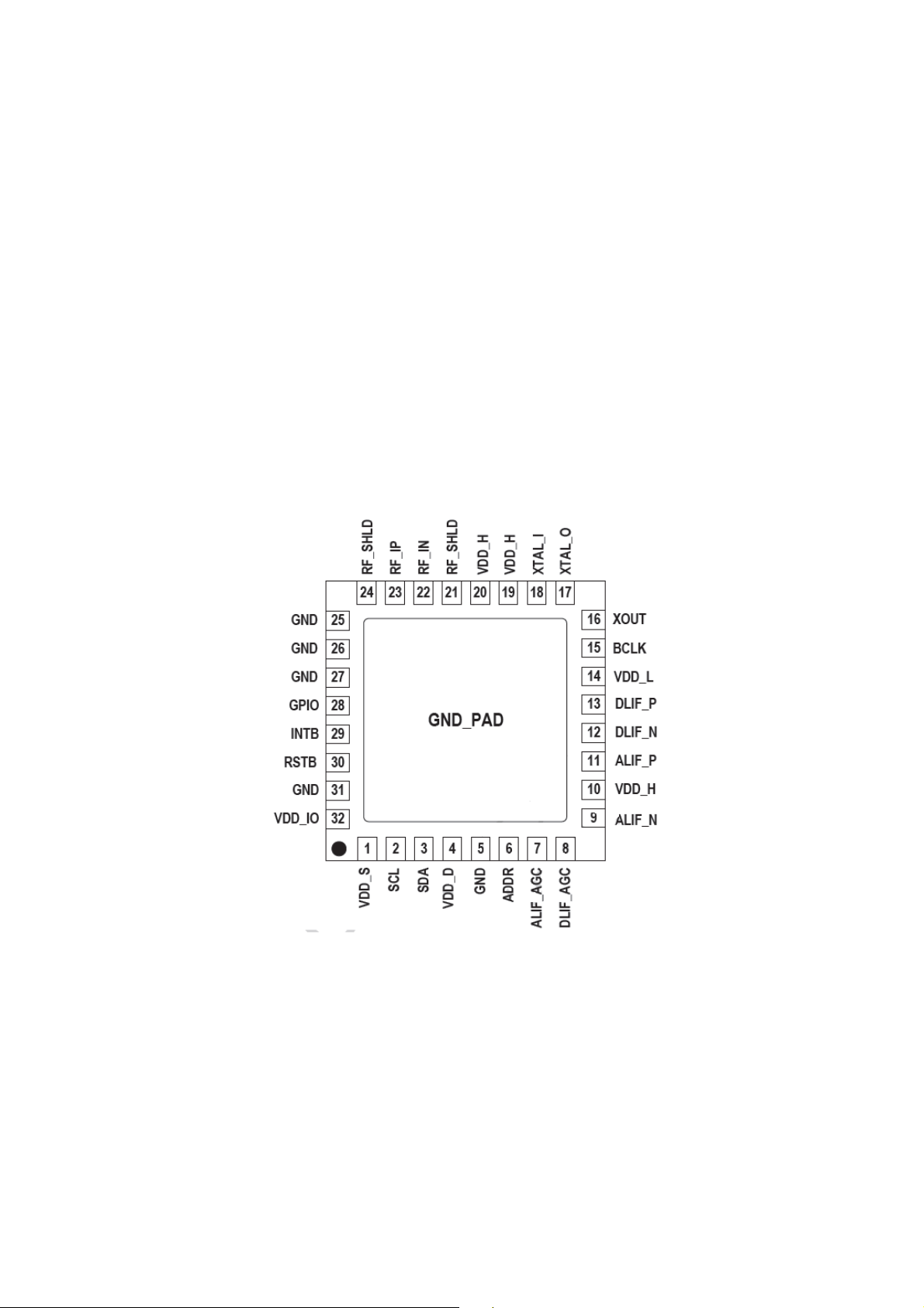
- 5 x 5 mm, 32-pin QFN package
- RoHS compliant
5
Figure 1: Pin description
Page 6
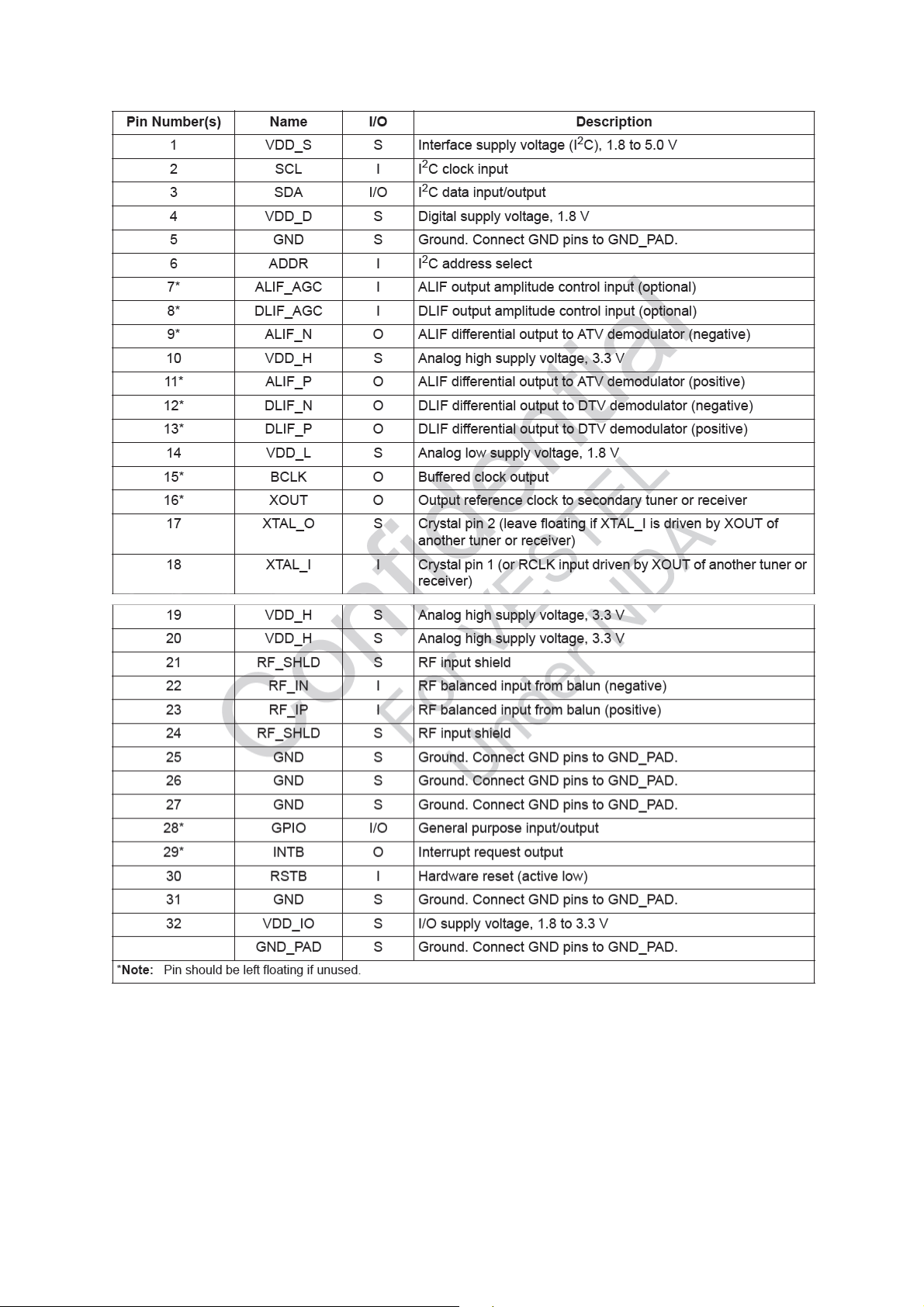
Table 1: Pin functions
6
Page 7

3. AUDIO AMPLIFIER STAGES
A. MAIN AMPLIFIER (TAS5719)(6-8 W option)
a. General Description
The TAS5717/TAS5719 is a 10-W/15-W, efficient,digital audio-power amplifier for
driving stereo bridge-tied speakers. One serial data input allows processing of up to two
discrete audio channels and seamless integration to most digital audio processors and MPEG
decoders. The device accepts a wide of input data and data rates. A fully programmable data
path routes these channels to the internal speaker drivers.
The TAS5717/9 is a slave-only device receiving all clocks from external sources. The
TAS5717/TAS5719 operates with a PWM carrier between a 384-kHz switching rate and a
352-KHz switching rate, depending on the input sample rate. Oversampling combined with a
fourth-order noise shaper provides a flat noise floor and excellent dynamic range from 20 Hz
to 20 kHz.
b. Features
• Audio Input/Output
– TAS5717 Supports 2×10 W and TAS5719 Supports 2×15 W Output
– Wide PVDD Range, From 4.5 V to 26 V
– Efficient Class-D Operation Eliminates Need for Heatsinks
– Requires Only 3.3 V and PVDD
– One Serial Audio Input (Two Audio Channels)
– I2C Address Selection via PIN (Chip Select)
– Supports 8-kHz to 48-kHz Sample Rate (LJ/RJ/I2S)
– External Headphone-Amplifier Shutdown Signal
– Integrated CAP-Free Headphone Amplifier
– Stereo Headphone (Stereo 2-V RMS Line Driver) Outputs
• Audio/PWM Processing
– Independent Channel Volume Controls With 24-dB to Mute
– Programmable Two-Band Dynamic Range Control
7
Page 8

– 14 Programmable Biquads for Speaker EQ
– Programmable Coefficients for DRC Filters
– DC Blocking Filters
– 0.125-dB Fine Volume Support
• General Features
– Serial Control Interface Operational Without MCLK
– Factory-Trimmed Internal Oscillator for Automatic Rate Detection
– Surface Mount, 48-Pin, 7-mm × 7-mm HTQFP Package
– AD, BD, and Ternary PWM-Mode Support
– Thermal and Short-Circuit Protection
• Benefits
– EQ: Speaker Equalization Improves Audio Performance
– DRC: Dynamic Range Compression. Can Be Used As Power Limiter. Enables
Speaker Protection, Easy Listening, Night-Mode Listening
– DirectPath Technology: Eliminates Bulky DC Blocking Capacitors
– Stereo Headphone/Stereo Line Drivers: Adjust Gain via External Resistors, Dedicated
Active Headpone Mute Pin, High Signal-to-Noise Ratio
– Two-Band DRC: Set Two Different Thresholds for Low- and High-Frequency
Content
8
Page 9
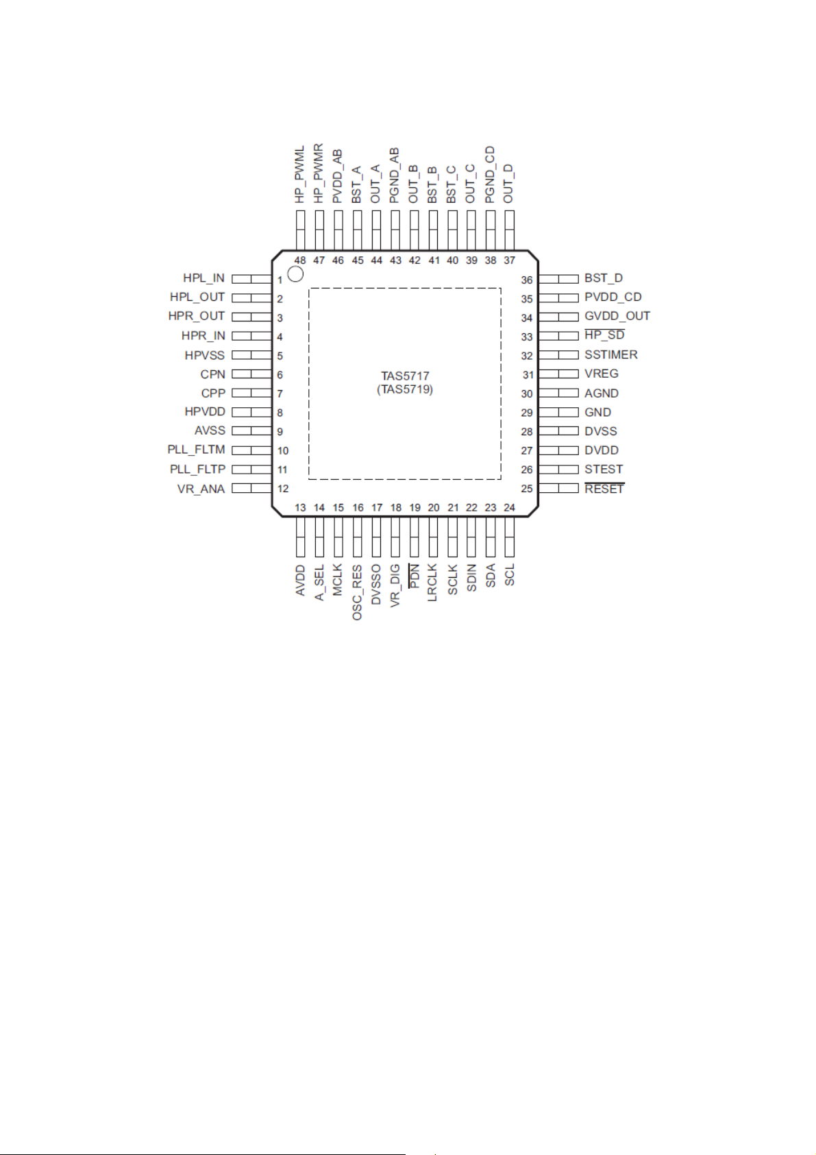
c. Pin descriptions and functions:
Figure 2: Pin description
9
Page 10
10
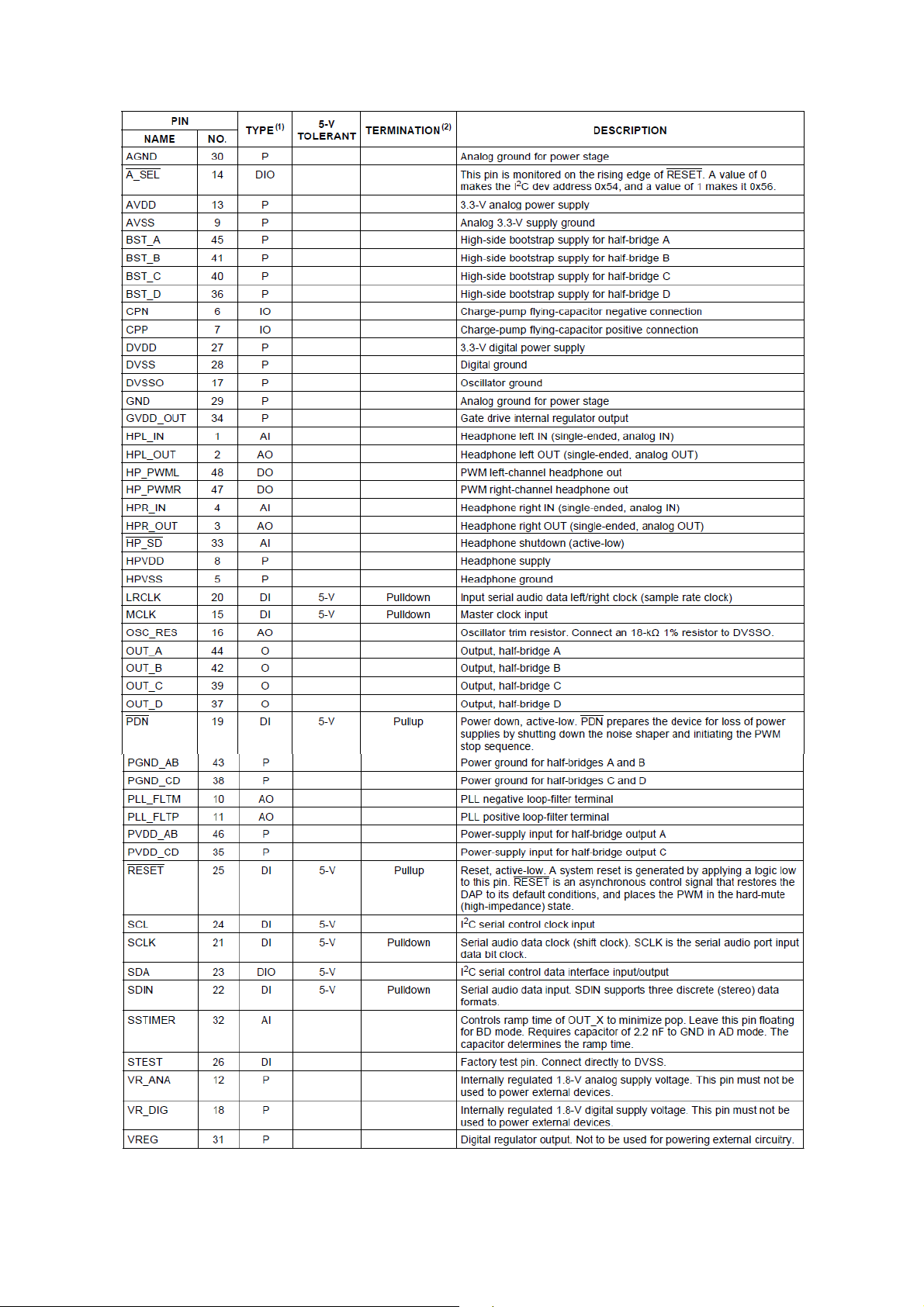
Table 2: Pin functions
Page 11
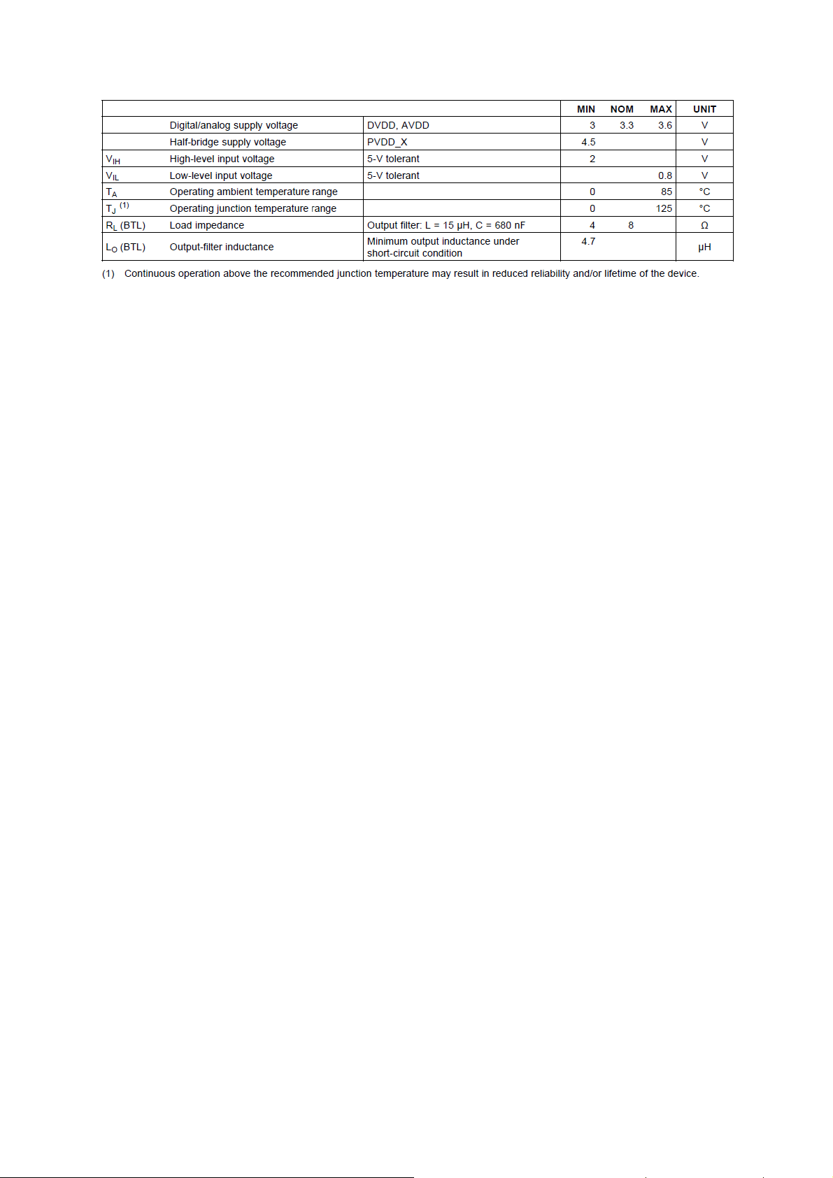
Table 3: Recomnended operating conditions
B. MAIN AMPLIFIER (TS4962M)(2.5 W option)
a. General Description
The TS4962M is a differential Class-D BTL power amplifier. It is able to drive up to 2.3W
into a 4Ω load and 1.4W into a 8Ω load at 5V. It achieves outstanding efficiency (88%typ.)
compared to classical Class-AB audio amps. The gain of the device can be controlled via two
external gain-setting resistors. Pop & click reduction circuitry provides low on/off switch
noise while allowing the device to start within 5ms. A standby function (active low) allows
the reduction of current consumption to 10nA typ.
b. Features
- Operating from VCC = 2.4V to 5.5V
- Standby mode active low
- Output power: 3W into 4Ω and 1.75W into 8Ω
- with 10% THD+N max and 5V power supply.
- Output power: 2.3W @5V or 0.75W @ 3.0V
- into 4Ω with 1% THD+N max.
- Output power: 1.4W @5V or 0.45W @ 3.0V
- into 8Ω with 1% THD+N max.
- Adjustable gain via external resistors
- Low current consumption 2mA @ 3V
- Efficiency: 88% typ.
- Signal to noise ratio: 85dB typ.
- PSRR: 63dB typ. @217Hz with 6dB gain
- PWM base frequency: 250kHz
11
Page 12
- Low pop & click noise
- Thermal shutdown protection
- Available in flip-chip 9 x 300
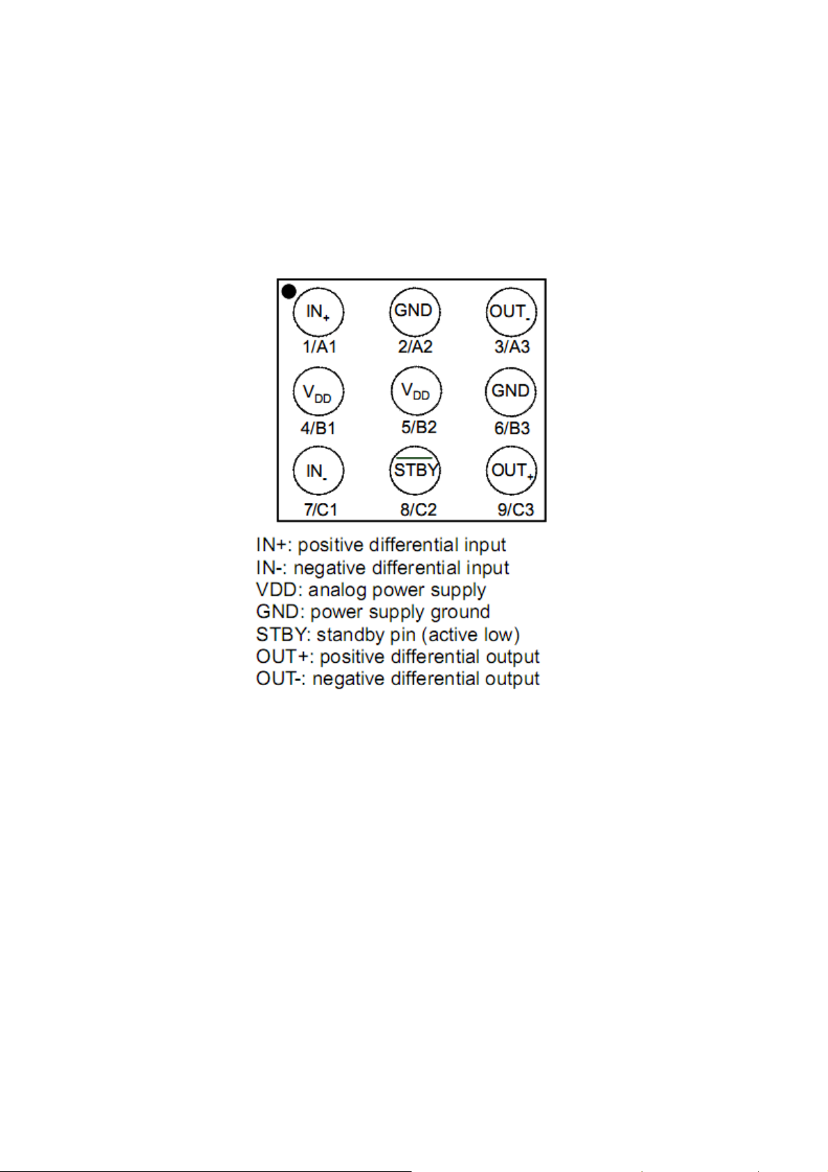
c. Pin descriptions and functions:
µm (Pb-free)
12
Figure 3: Pin description
Page 13
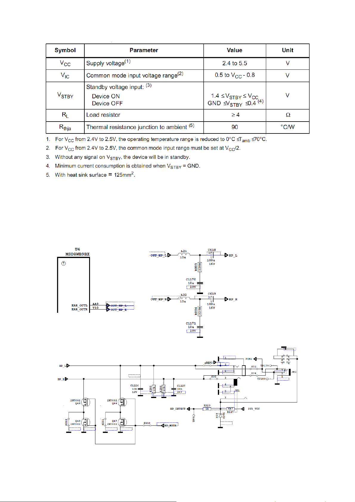
Table 4: Recommended operating conditions
C. HEADPHONE AMPLIFIER STAGE
Headphone is a SoC (single on chip) configuration in mainboard, design scheme is shown
in figure 4.
13
Figure 4: Headphone
Page 14
4. POWER STAGE
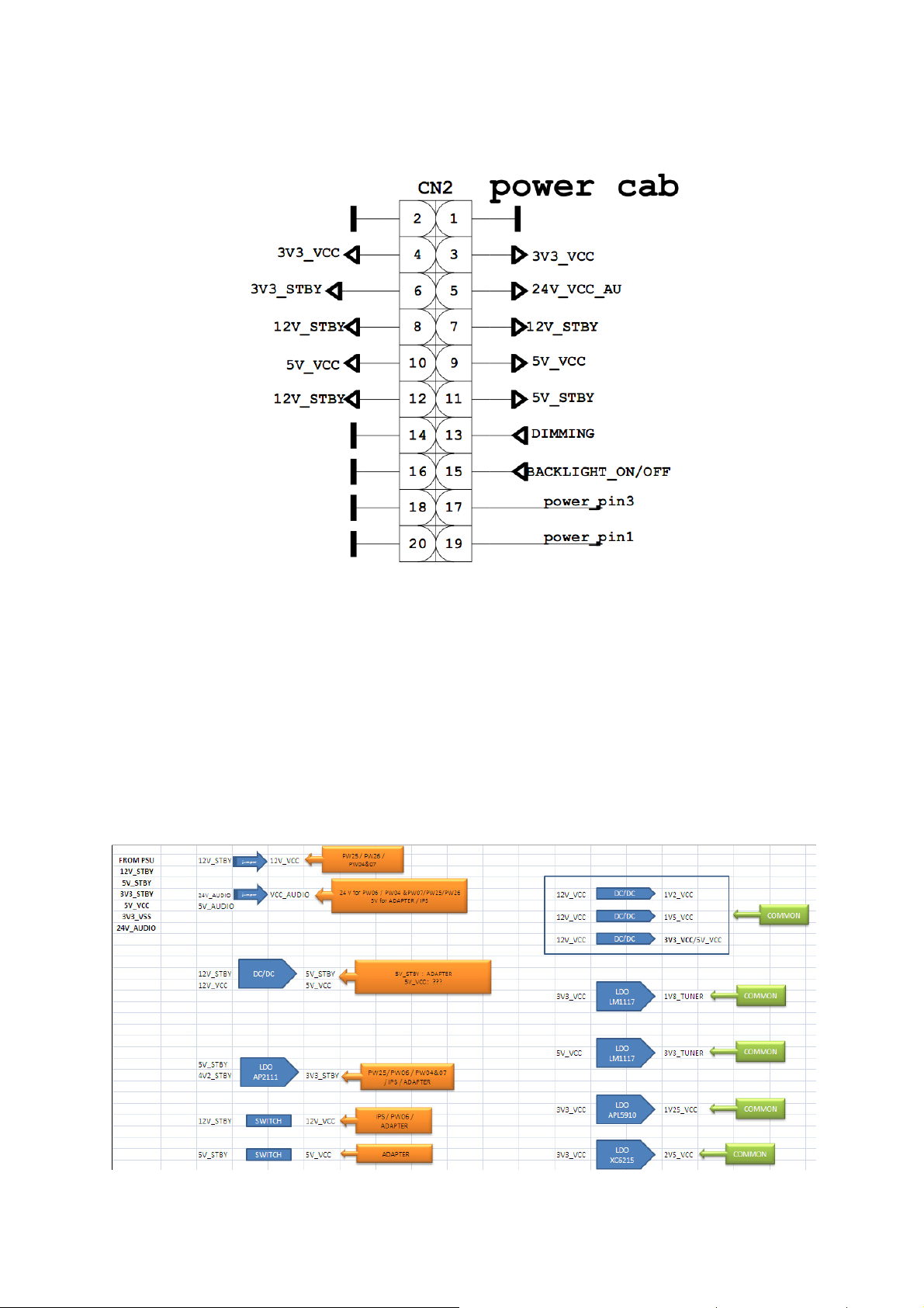
Figure 5: Power socket and power options
Power socket is used for taking voltages which are 3.3V, 12V, 5V and 24V(VDD_Audio).
These voltages are produced in power card. Also socket is used for giving dimming, backlight
and standbye signals with power card. İt is shown in figure 5.
24V(VDD_Audio) goes directly to the audio side, through power socket other incoming
voltages from power card are converted several voltages.
14
Figure 6: Power steps
Page 15
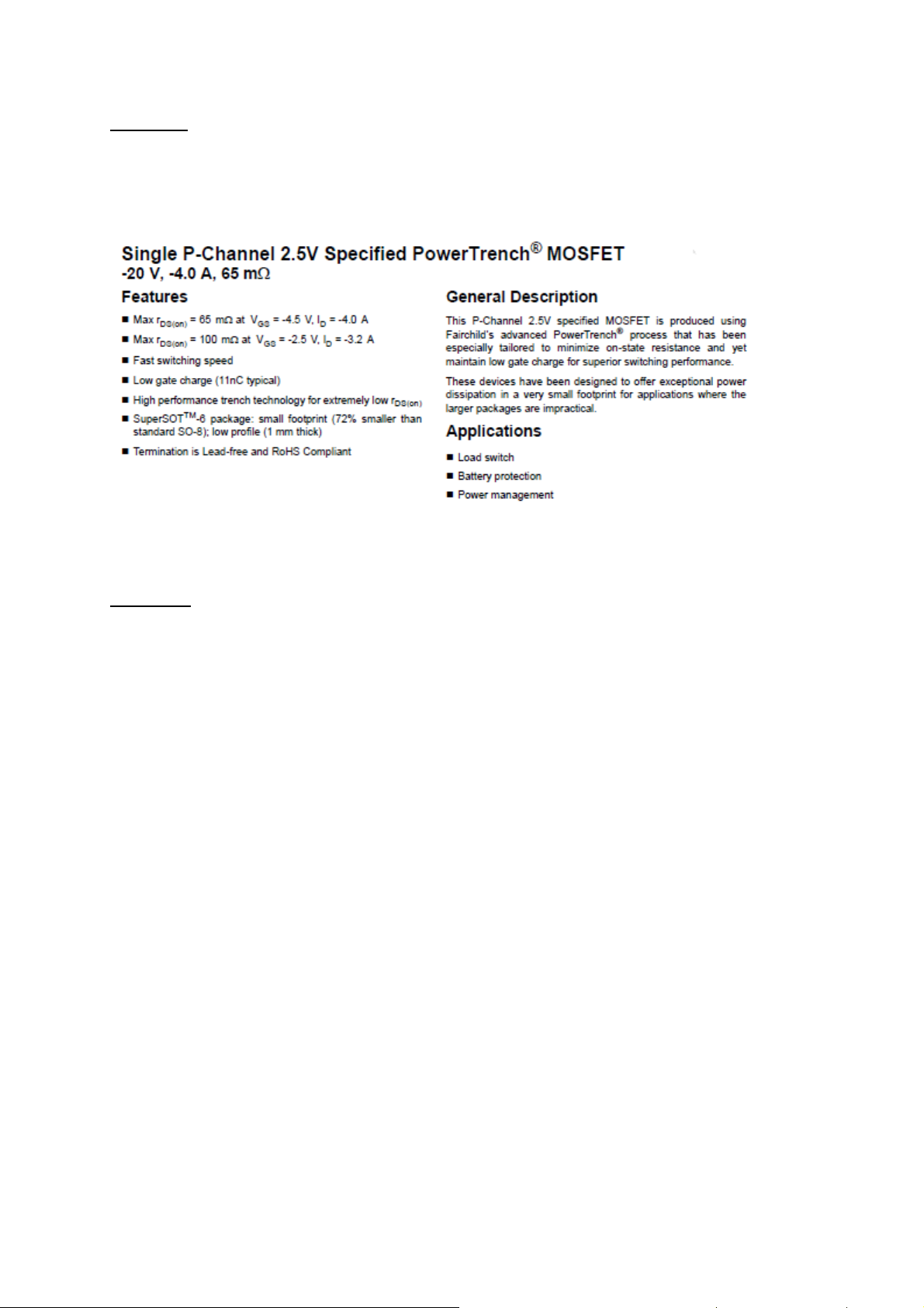
FDC642P
General Description and Features
TPS65251
a) General Description
The TPS65251 features three synchronous wide input range high efficiency buck
converters. The converters are designed to simplify its application while giving the designer
the option to optimize their usage according to the target application.
The converters can operate in 5-, 9-, 12- or 15-V systems and have integrated power
transistors. The output voltage can be set externally using a resistor divider to any value
between 0.8 V and close to the input supply. Each converter features enable pin that allows a
delayed start-up for sequencing purposes, soft start pin that allows adjustable soft-start time
by choosing the soft-start capacitor, and a current limit (RLIMx) pin that enables designer to
adjust current limit by selecting an external resistor and optimize the choice of inductor. The
current mode control allows a simple RC compensation.
The switching frequency of the converters can either be set with an external resistor
connected to ROSC pin or can be synchronized to an external clock connected to SYNC pin if
needed. The switching regulators are designed to operate from 300 kHz to 2.2 MHz. 180° out
of phase operation between Buck 1 and Buck 2, 3 (Buck 2 and 3 run in phase) minimizes the
input filter requirements.
15
Page 16

TPS65251 features a supervisor circuit that monitors each converter output. The PGOOD
pin is asserted once sequencing is done, all PG signals are reported and a selectable end of
reset time lapses. The polarity of the PGOOD signal is active high.
TPS65251 also features a light load pulse skipping mode (PSM) by allowing the LOW_P
pin tied to V3V. The PSM mode allows for a reduction on the input power supplied to the
system when the host processor is in stand-by (low activity) mode.
b) Features
• Wide Input Supply Voltage Range (4.5 V - 18 V)
• 0.8 V, 1% Accuracy Reference
• Continuous Loading: 3 A (Buck 1), 2 A (Buck 2 and 3)
• Maximum Current: 3.5 A (Buck 1), 2.5 A (Buck 2 and 3)
• Adjustable Switching Frequency 300 kHz - 2.2 MHz Set By External Resistor
• Dedicated Enable for Each Buck
• External Synchronization Pin for Oscillator
• External Enable/Sequencing and Soft Start Pins
• Adjustable Current Limit Set By External Resistor
• Soft Start Pins
• Current-Mode Control With Simple Compensation Circuit
• Power Good
• Optional Low Power Mode Operation for Light Loads
• QFN Package, 40-Pin 6 mm x 6 mm RHA
APPLICATIONS
• Set Top Boxes
• Blu-ray DVD
• Security Camera
• Car Audio/Video
• DTV
• DVR
16
Page 17
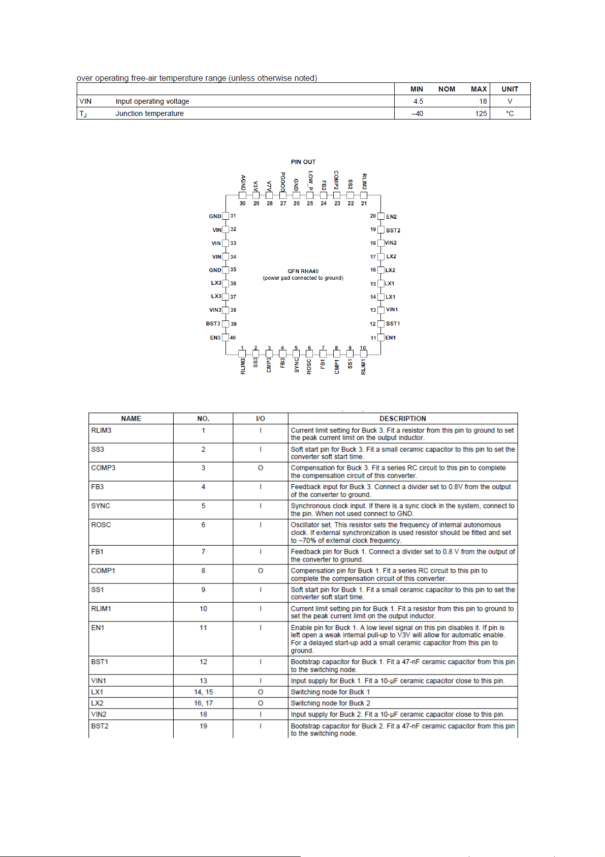
Table 5: Recommended operating conditions
Figure 7: Pin description
17
Page 18

Table 6: Pin functions
MP1484
a) General Description
The MP1484 is a monolithic synchronous buck regulator. The device integrates top and
bottom 85mΩ MOSFETS that provide 3A of continuous load current over a wide operating
input voltage of 4.75V to 18V. Current mode control provides fast transient response and
cycle-by-cycle current limit.
An adjustable soft-start prevents inrush current at turn-on and in shutdown mode, the
supply current drops below 1µA.
The MP1484 is PIN compatible to the MP1482 2A/18V/Synchronous Step-Down Converter.
b) Features
• 3A Continuous Output Current
• Wide 4.75V to 18V Operating Input Range
• Integrated 85m
Ω Power MOSFET Switches
18
Page 19

• Output Adjustable from 0.925V to 20V
• Up to 95% Efficiency
• Programmable Soft-Start
• Stable with Low ESR Ceramic Output Capacitors
• Fixed 340KHz Frequency
• Cycle-by-Cycle Over Current Protection
• Input Under Voltage Lockout
• Thermally Enhanced 8-Pin SOIC Package
APPLICATIONS
• FPGA, ASIC, DSP Power Supplies
• LCD TV
• Green Electronics/Appliances
• Notebook Computers
19
Figure 8: General description
Page 20

Table 7: Pin functions
APL5910
a) General Description
The APL5910 is a 1A ultra low dropout linear regulator. The IC needs two supply
voltages, one is a control voltage (VCNTL) for the control circuitry, the other is a main
supply voltage (VIN) for power conversion, to reduce power dissipation and provide
extremely low dropout voltage. The APL5910 integrates many functions. A Power-On- Reset
(POR) circuit monitors both supply voltages on VCNTL and VIN pins to prevent erroneous
operations. The functions of thermal shutdown and current-limit protect the device against
thermal and current over-loads. A POK indicates that the output voltage status with a delay
time set internally. It can control other converter for power sequence. The APL5910 can be
enabled by other power systems. Pulling and holding the EN voltage below 0.4V shuts off the
output.
The APL5910 is available in a SOP-8P package which features small size as SOP-8 and an
Exposed Pad to reduce the junction-to-case resistance to extend power range of applications.
b) Features
• Ultra Low Dropout
- 0.12V (Typical) at 1AOutput Current
• 0.8V Reference Voltage
• High Output Accuracy
- ±1.5%over Line, Load, and Temperature Range
20
Page 21

• Fast Transient Response
• Adjustable Output Voltage
• Power-On-Reset Monitoring on Both VCNTL and VIN Pins
• Internal Soft-Start
• Current-Limit and ShortCurrent-Limit Protections
• Thermal Shutdown with Hysteresis
• Open-Drain VOUT Voltage Indicator (POK)
• Low Shutdown Quiescent Current (< 30mA )
• Shutdown/Enable Control Function
• Simple SOP-8P Package with Exposed Pad
• Lead Free and Green Devices Available (RoHS Compliant)
APPLICATIONS
• Motherboards, VGA Cards
• Notebook PCs
• Add-in Cards
Figure 9: Pin configuration
21
Table 8: Recommended operating conditions
Page 22

Table 9: Pin description
LM1117
a) General Description
The LM1117 is a series of low dropout voltage regulators with a dropout of 1.2V at
800mA of load current. It has the same pin-out as National Semiconductor’s industry standard
LM317.
The LM1117 is available in an adjustable version, which can set the output voltage from
1.25V to 13.8V with only two external resistors. In addition, it is also available in five fixed
voltages, 1.8V, 2.5V, 2.85V, 3.3V, and 5V.
The LM1117 offers current limiting and thermal shutdown. Its circuit includes a zener
trimmed bandgap reference to assure output voltage accuracy to within ±1%.
The LM1117 series is available in LLP, TO-263, SOT-223, TO-220, and TO-252 D-PAK
packages. A minimum of 10µF tantalum capacitor is required at the output to improve the
transient response and stability.
b) Features
• Available in 1.8V, 2.5V, 2.85V, 3.3V, 5V, and Adjustable Versions
• Space Saving SOT-223 and LLP Packages
• Current Limiting and Thermal Protection
• Output Current 800mA
• Line Regulation 0.2% (Max)
• Load Regulation 0.4% (Max)
• Temperature Range:
22
Page 23

- LM1117 0˚C to 125˚C
- LM1117I −40˚C to 125˚C
• Applications
- 2.85V Model for SCSI-2 Active Termination
- Post Regulator for Switching DC/DC Converter
- High Efficiency Linear Regulators
- Battery Charger
- Battery Powered Instrumentation
5. MICROCONTROLLER (MSTAR MSD8WB9BX)
a) General Description
23
Page 24

b) Features
24
Page 25

25
Page 26

26
Page 27

Table 10: Recommended operating conditions
6. 1Gb DDR3 SDRAM
Hynix H5TQ1G630FA
a) Description
The H5TQ1G6(8)3DFR-xxx series are a 1,073,741,824-bit CMOS Double Data Rate III
(DDR3) Synchronous DRAM, ideally suited for the main memory applications which
requires large memory density and high bandwidth. Hynix 1Gb DDR3 SDRAMs offer fully
synchronous operations referenced to both rising and falling edges of the clock. While all
addresses and control inputs are latched on the rising edges of the CK (falling edges of the
CK), Data, Data strobes and Write data masks inputs are sampled on both rising and falling
edges of it. The data paths are internally pipelined and 8-bit prefetched to achieve very high
bandwidth.
b) Features
• DQ Power & Power supply : VDD & VDDQ = 1.5V +/- 0.075V
• DQ Ground supply : VSSQ = Ground
• Fully differential clock inputs (CK, CK) operation
• Differential Data Strobe (DQS, DQS)
• On chip DLL align DQ, DQS and DQS transition with CK transition
• DM masks write data-in at the both rising and falling edges of the data strobe
• All addresses and control inputs except data, data strobes and data masks latched on the
rising edges of the clock
• Programmable CAS latency 6, 7, 8, 9, 10, 11, 12, 13 and 14 supported
• Programmable additive latency 0, CL-1, and CL-2 supported
• Programmable CAS Write latency (CWL) = 5, 6, 7, 8, 9, 10
• Programmable burst length 4/8 with both nibble sequential and interleave mode
• Programmable PASR(Partial Array Self-Refresh) for Digital consumer Applications.
27
Page 28

• Programmable BL=4 supported (tCCD=2CLK) for Digi-tal consumer Applications.
• Programmable ZQ calibration supported
• BL switch on the fly
• 8banks
• Average Refresh Cycle (Tcase of 0 oC~ 95 oC)
- 7.8
- 3.9 µs at 85oC ~ 95 oC
- Commercial Temperature ( 0oC ~ 85 oC)
- Industrial Temperature ( -40oC ~ 85 oC)
• Auto Self Refresh supported
• JEDEC standard 78ball FBGA(x8), 96ball FBGA(x16)
• Driver strength selected by EMRS
• Dynamic On Die Termination supported
• Asynchronous RESET pin supported
• TDQS (Termination Data Strobe) supported (x8 only)
• Write Levelization supported
• On Die Thermal Sensor supported
• 8 bit pre-fetch
µs at -40oC ~ 85 oC
Table 11: Recommended operating conditions
7. 1Gb G-die DDR3 SDRAM
Samsung K4B1G1646G
a) Key Features
• JEDEC standard 1.5V ± 0.075V Power Supply
• VDDQ = 1.5V ± 0.075V
• 400 MHz fCK for 800Mb/sec/pin, 533MHz fCK for 1066Mb/sec/pin, 667MHz fCK for
1333Mb/sec/pin, 800MHz fCK for 1600Mb/sec/pin 900MHz fCK for 1866Mb/sec/pin
28
Page 29

• 8 Banks
• Programmable CAS Latency(posted CAS): 5,6,7,8,9,10,11,13
• Programmable Additive Latency: 0, CL-2 or CL-1 clock
• Programmable CAS Write Latency (CWL) = 5 (DDR3-800), 6 (DDR3-1066), 7 (DDR3-
1333), 8 (DDR3-1600) and 9 (DDR3-1866)
• 8-bit pre-fetch
• Burst Length: 8 (Interleave without any limit, sequential with starting address “000” only), 4
with tCCD = 4 which does not allow seamless read or write [either On the fly using A12 or
MRS]
• Bi-directional Differential Data-Strobe
• Internal(self) calibration : Internal self calibration through ZQ pin (RZQ : 240 ohm ± 1%)
• On Die Termination using ODT pin
• Average Refresh Period 7.8us at lower than TCASE 85°C, 3.9us at 85°C < TCASE < 95 °C
• Asynchronous Reset
• Package : 78 balls FBGA - x4/x8
• All of Lead-Free products are compliant for RoHS
• All of products are Halogen-free
Table 12: 1Gb DDR3 G-die Speed bins
b) Description
The 1Gb DDR3 SDRAM G-die is organized as a 32Mbit x 4 I/Os x 8banks, 16Mbit x 8
I/Os x 8banks device. This synchronous device achieves high speed double-data-rate transfer
rates of up to 1866Mb/sec/pin (DDR3- 1866) for general applications.
The chip is designed to comply with the following key DDR3 SDRAM fea-tures such as
posted CAS, Programmable CWL, Internal (Self) Calibration, On Die Termination using
ODT pin and Asynchronous Reset.
All of the control and address inputs are synchronized with a pair of exter-nally supplied
differential clocks. Inputs are latched at the crosspoint of dif-ferential clocks (CK rising and
29
Page 30

CK falling). All I/Os are synchronized with a pair of bidirectional strobes (DQS and DQS) in
a source synchronous fash-ion. The address bus is used to convey row, column, and bank
address information in a RAS/CAS multiplexing style. The DDR3 device operates with a
single 1.5V ± 0.075V power supply and 1.5V ± 0.075V VDDQ. The 1Gb DDR3 G-die device
is available in 78ball FBGAs(x4/x8).
Table 13: Absolute Maximum DC Ratings
Table 14: Recommended operating conditions
8. 2Gbit (256M x 8 bit) NAND Flash Memory
H27U2G8F2CTR-BC
a) Key Features
DENSITY
- 2Gbit: 2048blocks
Nand FLASH INTERFACE
- NAND Interface
- ADDRESS / DATA Multiplexing
SUPPLY VOLTAGE
- Vcc = 3.0/1.8V Volt core supply voltage for Program,
Erase and Read operations.
MEMORY CELL ARRAY
- X8: (2K + 64) bytes x 64 pages x 2048 blocks
- X16: (1k+32) words x 64 pages x 2048 blocks
PAGE SIZE
- X8: (2048 + 64 spare) bytes
30
Page 31

- X16:(1024 + 32spare) Words
Block SIZE
- X8: (128K + 4K spare) bytes
- X16:(64K + 2K spare) Words
PAGE READ / PROGRAM
- Random access: 25us (Max)
- Sequential access: 25ns / 45ns (3.0V/1.8V, min.)
- Program time(3.0V/1.8V): 200us / 250us (Typ)
- Multi-page program time (2 pages):
200us / 250us (3.0V/1.8V, Typ.)
BLOCK ERASE / MULTIPLE BLOCK ERASE
- Block erase time: 3.5 ms (Typ)
- Multi-block erase time (2 blocks):
3.5ms/ 3.5ms (3.0V/1.8V, Typ.)
SEQURITY
- OTP area
- Serial number (unique ID)
- Hardware program/erase disabled during Power transition
- Multiplane Architecture:
Array is split into two independent planes.
Parallel operations on both planes are available, having
program and erase time.
- Single and multiplane copy back program with automatic
EDC (error detection code)
- Single and multiplane page re-program
- Single and multiplane cache program
- Cache read
- Multiplane block erase
Reliability
- 100,000 Program / Erase cycles (with 1bit /528Byte ECC)
- 10 Year Data retention
ONFI 1.0 COMPLIANT COMMAND SET
ELECTRONICAL SIGNATURE
- Maunufacture ID: ADh
31
Page 32

- Device ID
PACKAGE
- Lead/Halogen Free
- TSOP48 12 x 20 x 1.2 mm
- FBGA63 9 x 11 x 1.0 mm
b) Description
H27(U_S)2G8_6F2C series is a 256Mx8bit with spare 8Mx8 bit capacity. The device is
offered in 3.0/1.8 Vcc Power Supply, and with x8 and x16 I/O interface Its NAND cell
provides the most cost-effective solution for the solid state mass storage market. The memory
is divided into blocks that can be erased independently so it is possible to preserve valid data
while old data is erased.
The device contains 2048 blocks, composed by 64 pages. Memory array is split into 2
planes, each of them consisting of 1024 blocks. Like all other 2KB - page NAND Flash
devices, a program operation allows to write the 2112-byte page in typical 200us(3.3V) and
an erase operation can be performed in typical 3.5ms on a 128K-byte block.
In addition to this, thanks to multi-plane architecture, it is possible to program 2 pages at a
time (one per each plane) or to erase 2 blocks at a time (again, one per each plane). As a
consequence, multi-plane architecture allows program time to be reduced by 40% and erase
time to be reduction by 50%. In case of multi-plane operation, there is small degradation at
1.8V application in terms of program/erase time.
The multiplane operations are supported both with traditional and ONFI 1.0 protocols.
Data in the page can be read out at 25ns (3V version) and 45ns (1.8V version) cycle time per
byte. The I/O pins serve as the ports for address and data input/output as well as command
input. This interface allows a reduced pin count and easy migration towards different
densities, without any rearrangement of footprint. Commands, Data and Addresses are
synchronously introduced using CE#, WE#, ALE and CLE input pin. The on-chip
Program/Erase Controller automates all read, program and erase functions including pulse
repetition, where required, and internal verification and margining of data.
A WP# pin is available to provide hardware protection against program and erase operations.
The output pin RB# (open drain buffer) signals the status of the device during each
operation. In a system with multiple memories the RB# pins can be connected all together to
provide a global status signal. Each block can be programmed and erased up to 100,000
cycles with ECC (error correction code) on. To extend the lifetime of Nand Flash devices, the
32
Page 33

implementation of an ECC is mandatory. The chip supports CE# don't care function. This
function allows the direct download of the code from the NAND Flash memory device by a
microcontroller, since the CE# transitions do not stop the read operation. In addition, device
supports ONFI 1.0 specification.
The copy back function allows the optimization of defective blocks management: when a
page program operation fails the data can be directly programmed in another page inside the
same array section without the time consuming serial
data insertion phase. Copy back operation automatically executes embedded error detection
operation: 1 bit error out of every 528-byte (x8) or 1 bit error out of every 264-word (x16) can
be detected. With this feature it is no longer necessary to use an external to detect copy back
operation errors. Multiplane copy back is also supported, both with traditional and ONFI 1.0
protocols. Data read out after copy back read (both for single and multiplane cases) is
allowed. In addition, Cache program and multi cache program operations improve the
programing throughput by programing data using the cache register.
The devices provide two innovative features: page re-program and multiplane page re
program. The page re-program allows to re-program one page. Normally, this operation is
performed after a previously failed page program operation.Similarly, the multiplane page re-
program allows to re-program two pages in parallel, one per each plane. The first page must
be in the first plane while the second page must be in the second plane; the multiplane page
re-program operation is performed after a previously failed multiplane page program
operation. The page re-program and multiplane page re-program guarantee imporve
performance, since data insertion can be omitted during re-program operations, and save ram
buffer at the host in the case of program failure. The devices, available in the TSOP48
(12X20mm) package, support the ONFI1.0 specfication and come with four sequrity features:
- OTP (one time programmable) area, which is a restricted access area where sensitive
data/code can be stored permantely.
- Serial number (unique identifier), which allows the devices to be uniquely indentified.
- Read ID2 extention
These security features are subject to an NDA (non-disclosure agreement) and are,
therefore, no described in the datasheet. For more details about them, contact your nearest
Hynix sales office.
33
Page 34

Table 15: DC and operating characteristic
9. 16M-BIT [16M x 1] CMOS SERIAL FLASH EEPROM
MX25L1602 Mstar SPI Flash
a) Key Features
■ HIGH DENSITY NAND FLASH MEMORIES
GENERAL
• 16,777,216 x 1 bit structure
• 256 Equal Sectors with 8K-byte each
- Any sector can be erased
• 4096 Equal Segments with 512-byte each
- Provides sequential output within any segment
• Single Power Supply Operation
- 3.0 to 3.6 volt for read, erase, and program operations
• Latch-up protected to 100mA from -1V to Vcc +1V
• Low Vcc write inhibit is equal to or less than 2.5V
34
Page 35

PERFORMANCE
• High Performance
- Fast access time: 20MHz serial clock (50pF + 1TTL Load)
- Fast program time: 5ms/page (typical, 128-byte per page)
- Fast erase time: 300ms/sector (typical, 8K-byte per sector)
• Low Power Consumption
- Low active read current: 10mA (typical) at 17MHz
- Low active programming current: 10mA (typical)
- Low active erase current: 10mA (typical)
- Low standby current: 30uA (typical, CMOS)
• Minimum 100,000 erase/program cycle
SOFTWARE FEATURES
• Input Data Format
- 1-byte Command code, 3-byte address, 1-byte byte address
• 512-byte Sequential Read Operation
• Built in 9-bit (A0 to A8) pre-settable address counter to support the 512-byte sequential read
operation
• Auto Erase and Auto Program Algorithm
- Automatically erases and verifies data at selected sector
- Automatically programs and verifies data at selected page by an internal algroithm
that automatically times the program pulse widths (Any page to be programed should have
page in the erased state first)
• Status Register Feature
- Provides detection of program and erase operation completion.
- Provides auto erase/ program error report
HARDWARE FEATURES
• SCLK Input
- Serial clock input
• SI Input
- Serial Data Input
• SO Output
- Serial Data Output
35
Page 36

• PACKAGE
- 28-pin SOP (330mil)
b) General Description
The MX25L1602 is a CMOS 16,777,216 bit serial Flash EEPROM, which is configured as
2,097,152 x 8 internally. The MX25L1602 features a serial peripheral interface and software
protocol allowing operation on a simple 3- wire bus. The three bus signals are a clock input
(SCLK), a serial data input (SI), and a serial data output (SO). SPI access to the device is
enabled by CS input.
The MX25L1602 provide sequential read operation on whole chip. The sequential read
operation is executed on a segment (512 byte) basis. User may start to read from any byte of
the segment. While the end of the segment is reached, the device will wrap around to the
beginning of the segment and continuously outputs data until CS goes high.
After program/erase command is issued, auto program/ erase algorithms which
program/erase and verify the specified page locations will be executed. Program command is
executed on a page (128 bytes) basis, and erase command is executed on both chip and sector
(8K bytes) basis.
To provide user with ease of interface, a status register is included to indicate the status of
the chip. The status read command can be issued to detect completion and error flag status of
a program or erase operation.
When the device is not in operation and CS is high, it is put in standby mode and draws
less than 30uA DC current.
The MX25L1602 utilizes MXIC's proprietary memory cell which reliably stores memory
contents even after 100,000 program and erase cycles.
36
Page 37

Figure: Pin configuration.
Table 16: Pin description
10. USB Interface
Mstar IC has two input port for USB, therefore air mause, internal wi-fi interface and
USB2 are combined with HUB. This property is optional. If air mause and wi-fi interfaces are
not alined, two USB are connected directly to main IC.
37
Page 38

Figure 10: USB description
USB2512B
a) General Description
The SMSC USB251xB/xBi hub is a family of low-power, configurable, MTT (multi
transaction translator) hub controller IC products for embedded USB solutions. The x in the
part number indicates the number of downstream ports available, while the B indicates battery
charging support. The SMSC hub supports lowspeed, full-speed, and hi-speed (if operating as
a hispeed hub) downstream devices on all of the enabled downstream ports.
b) Features
- USB251xB/xBi products are fully footprint compatible with USB251x/xi/xA/xAi
products as direct drop-in replacements
• Cost savings include using the same PCB components and application of
USB-IF Compliance by Similarity
- Full power management with individual or ganged power control of each downstream
port
- Fully integrated USB termination and pull-up/pulldown resistors
- Supports a single external 3.3 V supply source; internal regulators provide 1.2 V
internal core voltage
- Onboard 24 MHz crystal driver, ceramic resonator, or external 24/48 MHz clock input
- Customizable vendor ID, product ID, and device ID
- 4 kilovolts of HBM JESD22-A114F ESD protection (powered and unpowered)
- Supports self- or bus-powered operation
38
Page 39

- Supports the USB Battery Charging specification Rev. 1.1 for Charging Downstream
Ports (CDP)
- 36-pin QFN (6x6 mm) Lead-free RoHS compliant package
- USB251xBi products support the industrial temperature range of -40ºC to +85ºC
- USB251xB products support the extended commercial temperature range of 0ºC to
+85ºC
c) Applications
- LCD monitors and TVs
- Multi-function USB peripherals
- PC motherboards
- Set-top boxes, DVD players, DVR/PVR
- Printers and scanners
- PC media drive bay
- Portable hub boxes
- Mobile PC docking
- Embedded systems
39
Figure 11: Pin configurations
Page 40

11. CI Interface
17MB95S Digital CI ve Smart Card Interface Block diagram:
Figure 12: CI interface
12. Software Update
12.1 Main SW update
In MB95 project there is only one software. From following steps software update procedure
can be seen:
1. MB90_en.bin, mboot.bin and usb_auto_update_A1.txt documents should copy directly
inside of a flash memory(not in a folder).
2. Insert flash memory to the tv when tv is powered off.
3. While pushing the OK button in remote control, power on the and wait. TV will power-up
itself.
4. If First Time Installation screen comes, it means software update procedure is successful.
13. Troubleshooting
A. No Backlight Problem
Problem: If TV is working, led is normal and there is no picture and backlight on the panel.
Possible couses: Backlight pin, dimming pin, backlight supply, stby on/off pin
40
Page 41

BACKLIGHT_ON/OFF pin should be high when the backlight is ON. R119 must be low
when the backlight is OFF. If it is a problem, please check Q10 and the panel cables. Also it
can be tested in TP50 in main board.
Dimming pin should be high or square wave in open position. If it is low, please check S60
for Mstar side and panel or power cables, connectors.
Backlight power supply should be in panel specs. Please check Q33, shown below; also it can
be checked TP53.
41
Page 42

STBY_ON/OFF_NOT should be low for tv on condition, please check Q11’s collector.
B. CI Module Problem
Problem: CI is not working when CI module inserted.
Possible couses: Supply, suply control pin, detect pins, mechanical positions of pins.
• CI supply should be 5V when CI module inserted. If it is not 5V please check
CI_PWR_CTRL, this pin should be low.
42
Page 43

• Please check mechanical position of CI module. Is it inserted properly or not?
• Detect ports should be low. If it is not low please check CI connector pins, CI module
pins.
43
Page 44

C. Staying in Stand-by Mode
Problem: Staying in stand-by mode, no other operation
This problem indicates a short on Vcc voltages. Protect pin should be logic high while normal
operation. When there is a short circuit protect pin will be logic low. If you detect logic low
on protect pin, unplug the TV set and control voltage points with a multimeter to find the
shorted voltage to ground.
44
Page 45

D. IR Problem
Problem: LED or IR not working
Check LED card supply on MB95 chasis.
E. Keypad Touchpad Problems
Problem: Keypad or Touchpad is not working
Check keypad supply on MB95.
45
Page 46

46
Page 47

F. USB Problems
Problem: USB is not working or no USB Detection.
Check USB Supply, It should be nearly 5V. Also USB Enable should be logic high.
G. No Sound Problem
Problem: No audio at main TV speaker outputs.
Check supply voltages of 24V VDD_AUDIO, 3.3V AUDIO_AVDD and AUDIO_DVDD
with a voltage-meter. There may be a problem in headphone connector or headphone detect
circuit (when headphone is connected, speakers are automatically muted). Measure voltage at
HP_DETECT pin, it should be 3.3v.
47
Page 48

H. Standby On/Off Problem
Problem: Device can not boot, TV hangs in standby mode.
There may be a problem about power supply. Check main supplies with a voltage-meter. Also
there may be a problem about SW. Try to update TV with latest SW. Additionally it is good
to check SW printouts via Teraterm. These printouts may give a clue about the problem. You
can use Scart-1 for terraterm connection.
İ. No Signal Problem
Problem: No signal in TV mode.
Check tuner supply voltage; 5V_VCC, 3V3_TUNER and 1V8_TUNER. Check tuner options
are correctly set in Service menu. Check AGC voltage at IF_AGC pin of tuner.
14. Service Menu Settings
In order to reach service menu, first Press “MENU” buton, then write “4725” by uisng
remote controller.
You can see the service menu main screen below. You can check SW releases by using this
menu. In addition, you can make changes on video, audio etc. by using video settings, audio
settings titles.
48
Page 49

Service Menu Main Screen
Video Settings
49
Page 50

Audio Settings
Options-1 Menu
50
Page 51

Options-2 Menu
Options-3 Menu
51
Page 52

Tuner Settings Menu
Source Settings Menu
52
Page 53

Diagnostic Menu
53
Page 54

15. General Block Diagram
54
 Loading...