


TABLE OF CONTENTS
1. INTRODUCTION ...................................................................................................................... 3
1.1. General Block Diagram .................................................................................................. 4
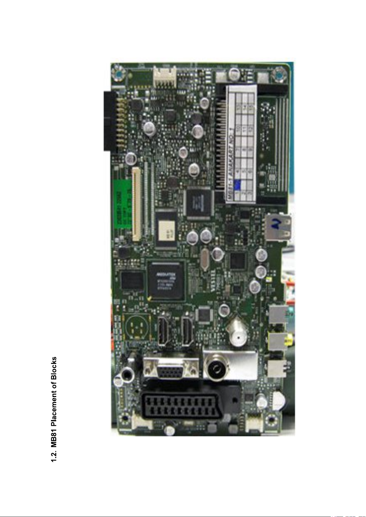
1.2. MB8
1. TUNER(S
M88TS2022 (Optional) ...................................................................................................................... 7
M88DS3002 (Optional) ...................................................................................................................... 9
2. AUDIO AMPLIFIER STAGE ................................................................................................. 11
STA381BWS ............................................................................................................................ 11
2.1. General Description ...................................................................................................... 11
2.2. Features ........................................................................................................................ 11
2.3. Absolute Ratings .......................................................................................................... 13
2.3.1. Electrical Characteristics .......................................................................................... 13
2.3.2. Operating Specifications .......................................................................................... 13
2.4. Pinning ......................................................................................................................... 14
TS4962M (Optional 2,5W) ...................................................................................................... 17
3. POWER STAGE ...................................................................................................................... 18
3.1. Power Management ...................................................................................................... 20
MICROCONTROLLER MediaTek ...................................................................................... 21
4.
4.1. Description ................................................................................................................... 21
MT5365 (Main IC) (U1) .............................................................................................................. 21
4.2. MediaTek Block Diagram ............................................................................................ 28
4.3. Reset Circuit ................................................................................................................. 29
5. CI INTERFACE ....................................................................................................................... 29
CI Interface Power Switch: ...................................................................................................... 29
6. USB INTERFACE ................................................................................................................... 30
7. DDR3 SDRAM NTC-DDR3-1Gb-D-R12 ........................................................................... 30
Description: .................................................................................................................................. 30
Features: ................................................................................................................................... 31
8. SCALER AND LVDS SOCKETS ........................................................................................... 33
8.1. LVDS sockets Block Diagram ..................................................................................... 33
8.2. Panel Supply Switch Circuit ........................................................................................ 34
NAND FLASH MEMORY K9F1G08U0D .......................................................................... 34
9.
9.1. General Description ...................................................................................................... 34
9.2. Features ........................................................................................................................ 35
9.3. Pinning ......................................................................................................................... 35
10. I-LM1117/LM 800mA Low-Dropout Linear Regulator ...................................................... 36
11. CONNECTORS ................................................................................................................... 37
11.1. SCART (SC1) .............................................................................................................. 37
11.2. HDMI (CN707,CN708) ............................................................................................... 37
11.3. VGA (CN711) .............................................................................................................. 38
12. SERVICE MENU SETTINGS ............................................................................................. 39
12.1. Video Settings .............................................................................................................. 40
12.2. Audio Settings .............................................................................................................. 41
12.3. Options ......................................................................................................................... 42
12.4. Tuning Settings ............................................................................................................ 44
12.5. Source Settings ............................................................................................................. 45
12.6. Diagnostic ..................................................................................................................... 46
12.7. USB Operations ............................................................................................................ 47
Placement of Blocks ............................................................................................ 5
2156) ........................................................................................................................ 6

13. SOFTWARE UPDATE ........................................................................................................ 47
14. TROUBLESHOOTING ....................................................................................................... 47
14.1. No Backlight Problem .................................................................................................. 47
14.2. CI Module Problem ...................................................................................................... 49
14.3. Led Blinking Problem .................................................................................................. 50
14.4. IR Problem ................................................................................................................... 51
14.5. Keypad Touchpad Problems ........................................................................................ 52
14.6. USB Problems .............................................................................................................. 52
14.7. No Sound Problem ....................................................................................................... 53
14.8. No Sound Problem at Headphone ................................................................................ 53
14.9. Standby On/Off Problem .............................................................................................. 53
14.10. No Signal Problem ................................................................................................... 54
1. INTRODUCTION
17MB8 mainboard is driven by MediaTek MT5356. This IC is capable of handling Video
and audio processing, Scaling-Display processing, 3D comb filter, OSD and text
processing, LVDS/mini-LVDS transmitting, channel and MPEG2/4 decoding, integrated
DVB-T/C demodulator and media center functionality.
TV supports PAL, SECAM, NTSC colour standards and multiple transmission standards
as B/G, D/K, I/I, and L/L including German and NICAM stereo. Also DVB T, DVB-C are
supported internal demoulators of MediaTek IC and DVB-S/S2 is supported with externall
demodulator.
Sound system output is supplying max. 2x8W ( less 10%THD at max output) for stereo
speakers.
8
Supported peripherals are:
1 RF input VHF I, VHF III, UHF @ 75Ohm(Common)
1 Side AV (CVBS, R/L_Audio)
1 SCART socket(Common)
1 YPbPr (Optional)
1 PC input(Common)
2 HDMI 1.3 input(1 HDMI input is common, 1 input is optional)
1 S/PDIF output(Optional)
1 Headphone(Optional)
1 Common interface(Common)
1 USB input is
1 On-board Keypad(Optional)
1 External Keypad(Optional)
1 External TouchPad(Optional)
ommon)
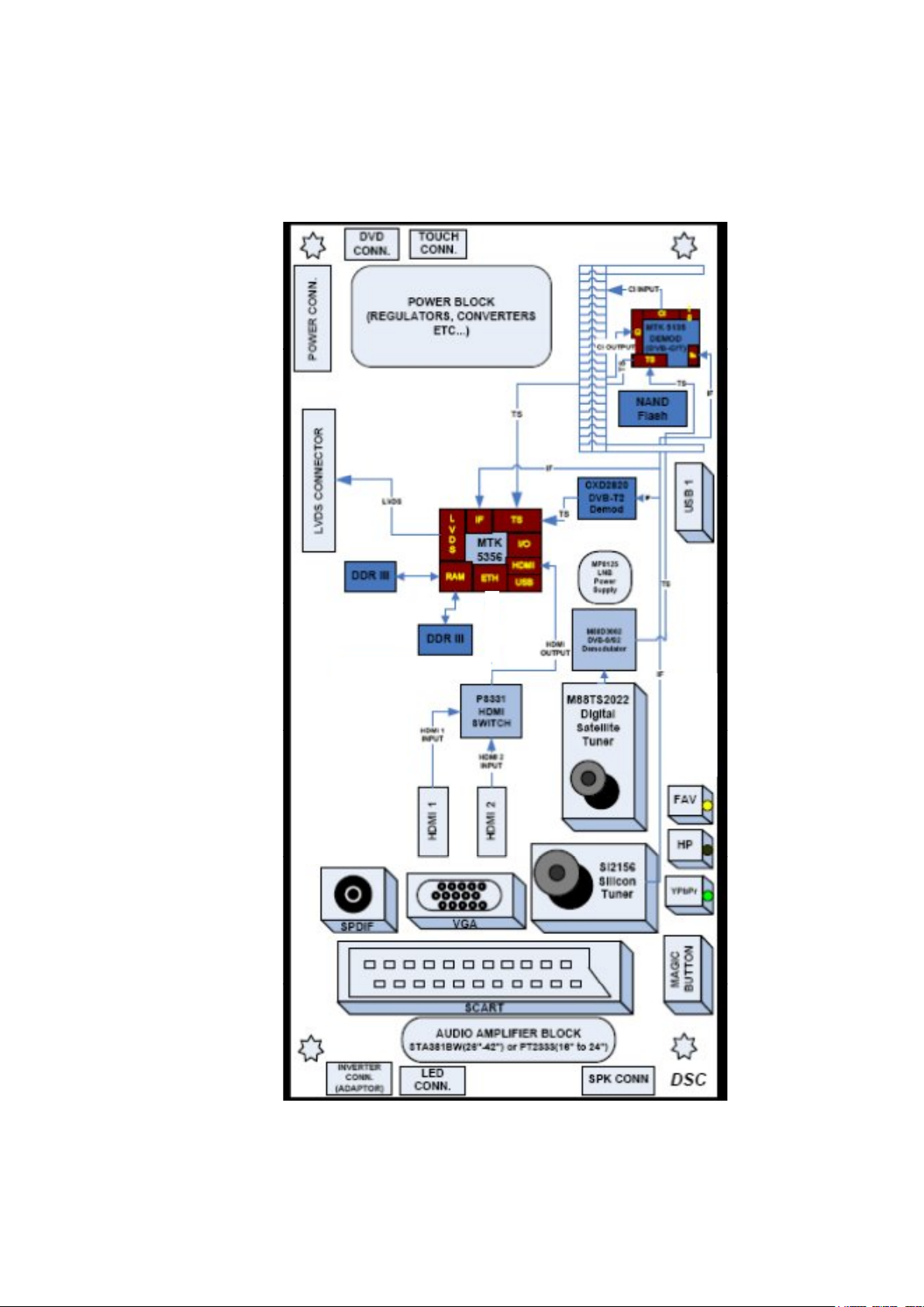
1.1. General Block Diagram
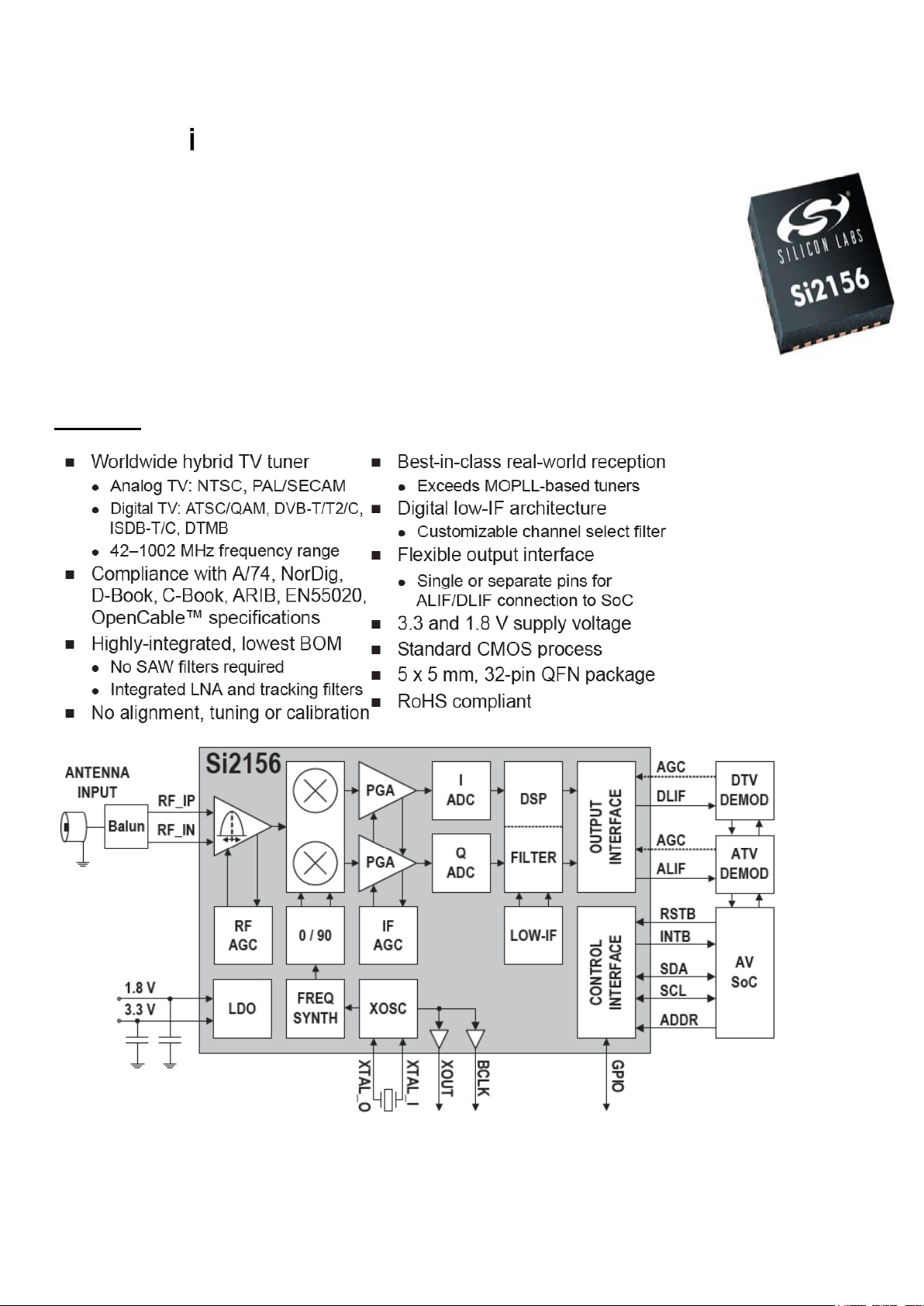
1. TUNER(S 2156)
The Si2156 integrates a complete hybrid TV tuner supporting all worldwide
terrestrial and cable TV standards. Lever
generation digital low-IF architecture, the Si2156 maintains the unmatched
performance and design simplicity of the original Si2153 while further reducing
footprint size. No external LNAs, tracking filters, or SAW filters are used. Compared
with competing silicon tuners and discrete MOPLL-based tuners, the Si2156
delivers superior picture quality and a higher number of received stations in realworld conditions due to its very high linearity and low noise. Interfacing the Si2156
seamlessly with the Si2165 DVB-T/C demodulator creates a DVB-T/C receiver plus
PAL/SECAM tuner. The Si2156 is pin-compatible with the Si2176 hybrid TV tuner
with analog demodulator, providing customers unparalleled design flexibility.
Features :
aging Silicon Labs field proven third
BLOCK DIADRAM
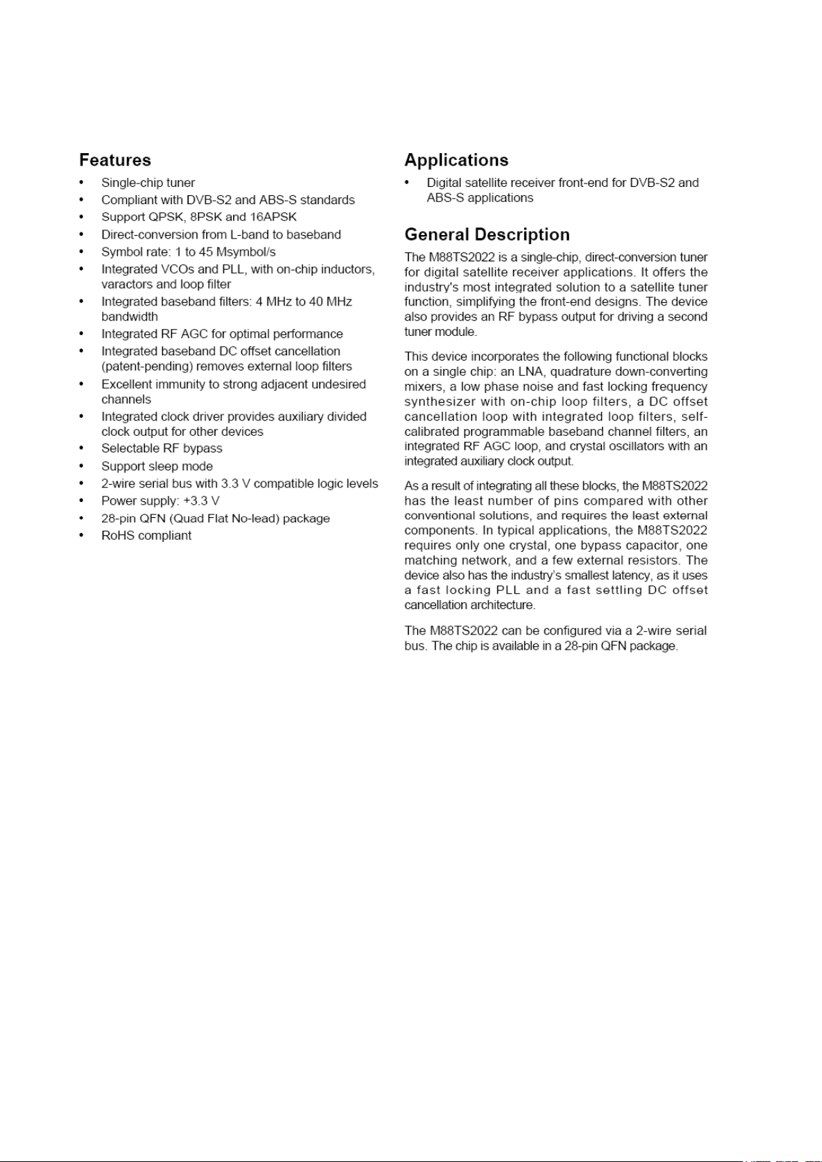
M88TS2022 (Optional)
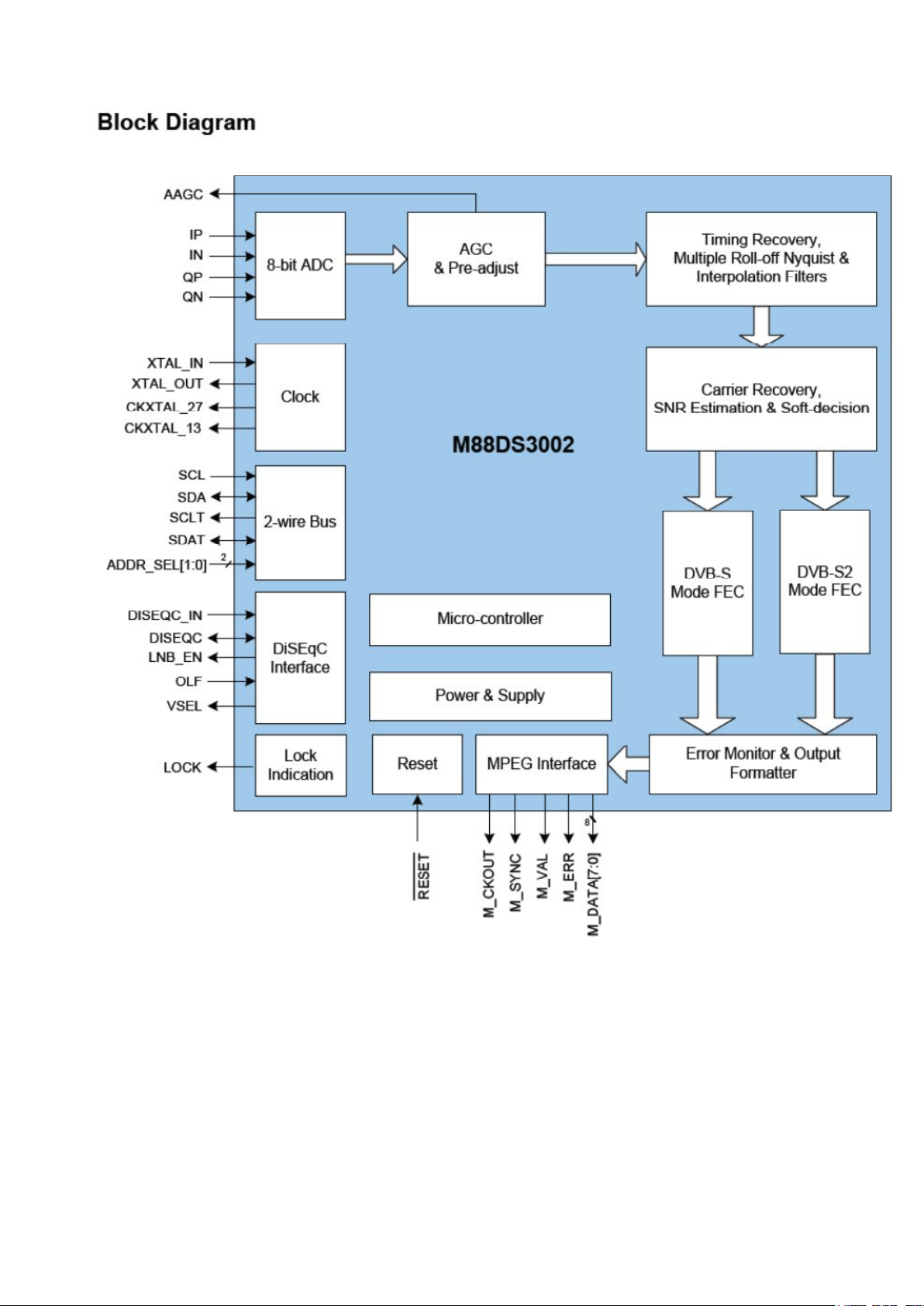
M88DS3002 (Optional)

2. AUDIO AMPLIFIER STAGE
STA381BWS
2.1. General Description
The STA381BWS is an integrated solution embedding digital audio processing, digital amplification,
FFXTM power output stage, headphone and 2 Vrms line outputs. It is part of the Sound Terminal®
family and provides full digital audio streaming from the source to the speaker, offering cost
effectiveness, low power dissipation and sound enrichment.
The STA381BWS input section consists of a flexible digital input serial audio interface, feeding the
digital processing unit, and an analog 1 Vrms input for a seamless connection with pure analog
sources. The serial audio data input interface supports many formats, including the popular IIS
format.
The STA381BWS is based on an FFXTM (Fully Flexible Amplification) processor, an
STMicroelectronics proprietary technology. FFXTM is the evolution of the ST ternary technology: the
advanced processor is available for ternary, binary, binary differential and phase shift PWM
modulation. STA381BWS embeds the ternary, binary and binary differential implementations, a
subset of the full capability of the FFXTM processor.
The STA381BWS power section consists of four independent half-bridges. These can be configured
via digital control to operate in different modes. A 2.1 channel setup can be implemented with two
half-bridges (L/R) together with a single full-bridge (subwoofer).
Alternatively, the 2.0 channel setup can be done with two full-bridges. When using this configuration
an external amplifier, for the SW channel, can be also driven through the PWM output. The
STA381BWS is able to deliver 2 x 20 W (ternary) into an 8 W load at 18 V or 2 x 9 W (binary) into a 4
W load plus 1 x 20 W (ternary) into an 8 W load at 18 V. The STA381BWS also provides a capless
headphone out (with embedded negative charge pump), able to deliver up to 40 mW into a 32 W
load or, alternatively, can be configured as a 2 Vrms line output.
The STA381BWS digital processing unit includes up to 12 programmable biquads (EQs) allowing
perfect sound equalization and offering advanced noise-shaping techniques.
Moreover, the coefficient range ensures a great variety of filter shapes (low/high-pass, low/high shelf,
peak, notch, band-pass). The equalization engine is fully compatible with the ST speaker
compensation technology embedded into the APWorkbench suite. A state-ofthe- art multi-band DRC,
STCompressorTM, equalizes the system to provide active speaker protection with full audio quality
preservation against sudden sound peaks. Moreover, STSpeakerSafeTM technology offers reliable
speaker protection under any condition. The master clock can be from stable BICKI (64xfs, 50% duty
cycle) or external XTI.
2.2. Features
Features
Wide-range supply voltage
4.5 V to 25.5 V (operating range)
27 V (absolute maximum rating)
I2C control with selectable device address
Full IC protection embedding:
Manufacturing short-circuit protection (out
vs. gnd, out vs. vcc, out vs. out)
Thermal protection
Overcurrent protection
Undervoltage protection

1 Vrms stereo analog input
I2S interface, sampling rate 32 kHz ~ 192 kHz,
with internal sampling frequency converter for
fixed processing frequency
Three output power stage configurations
2.0 mode, L/R full bridges
2.1 mode, L/R two half-bridges, subwoofer
full bridge
2.1 mode, L/R full bridges, PWM output for
external subwoofer amplifier
Driving load capabilities
2 x 20 W into 8 W ternary modulation
2 x 9 W into 4 W + 1 x 20 W into 8 W
FFXTM 100 dB dynamic range
Fixed output PWM frequency at any input
sampling frequency
Embedded RMS meter for measuring real-time
loudness
Two analog outputs:
Selectable headphone / line out driver with
adjustable gain via external resistors
Auxiliary F3XTM analog output for external
driver
Headphone:
Embedded negative charge pump
Full capless output configuration
Driving load capabilities: 40 mW into 32 W
Line out:
2 Vrms line output capability
Up to 12 user-programmable biquads with
noise-shaping technology
Direct access to coefficients through I2C
shadowing mechanism
Fixed (88.2 kHz / 96 kHz) internal processing
sampling rate
Two independent DRCs configurable as a
dual-band anticlipper or independent
limiters/compressors (B2DRC)
Digital gain/att +48 dB to -80 dB with
0.125 dB/step resolution
Independent (fade in, fade out) soft volume
update with programmable rate 48 ~ 1.5 dB/ms
Bass/treble tones control
Audio presets:15 crossover filters, 5
anticlipping modes, nighttime listening mode
STSpeakerSafeTM protection circuitry:
Pre and post processing DC blocking filters
Checksum engine for filter coefficients
PWM fault self-diagnosis
STCompressorTM dual-band DRC
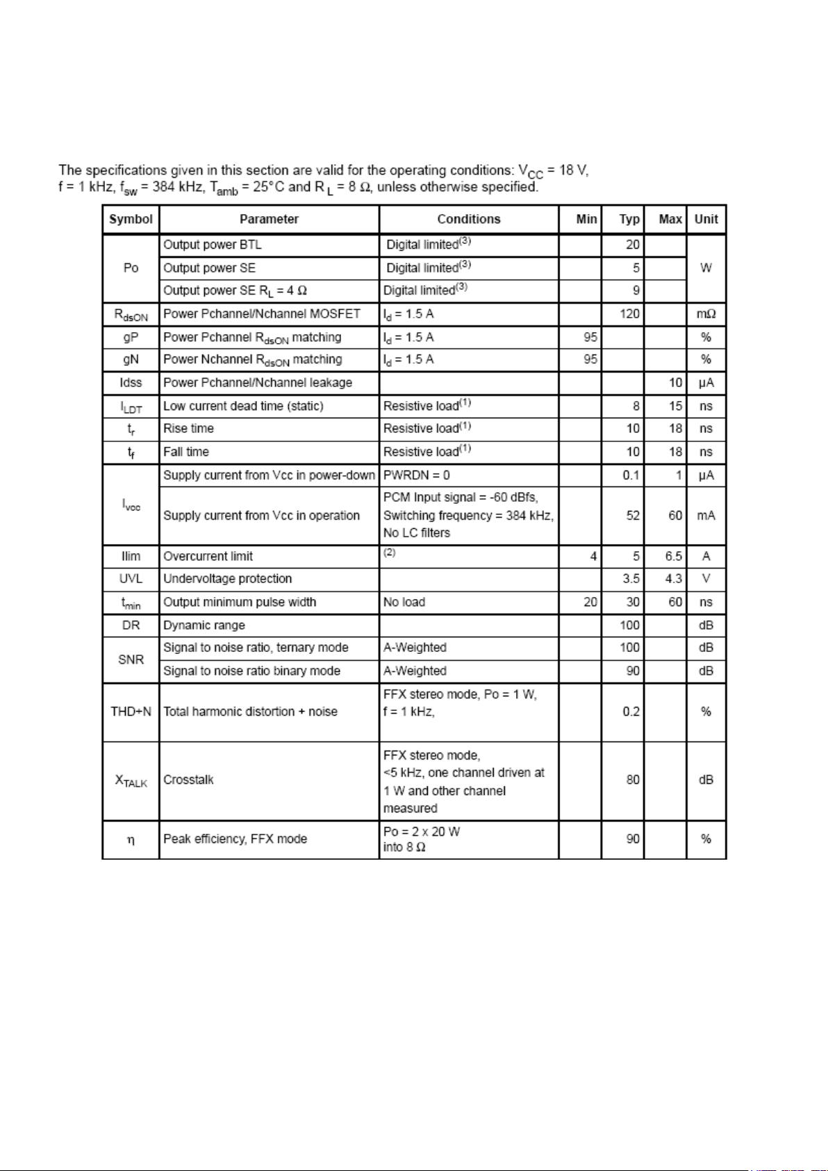
2.3. Absolute Ratings
2.3.1. Electrical Characteristics
2.3.2. Operating Specifications
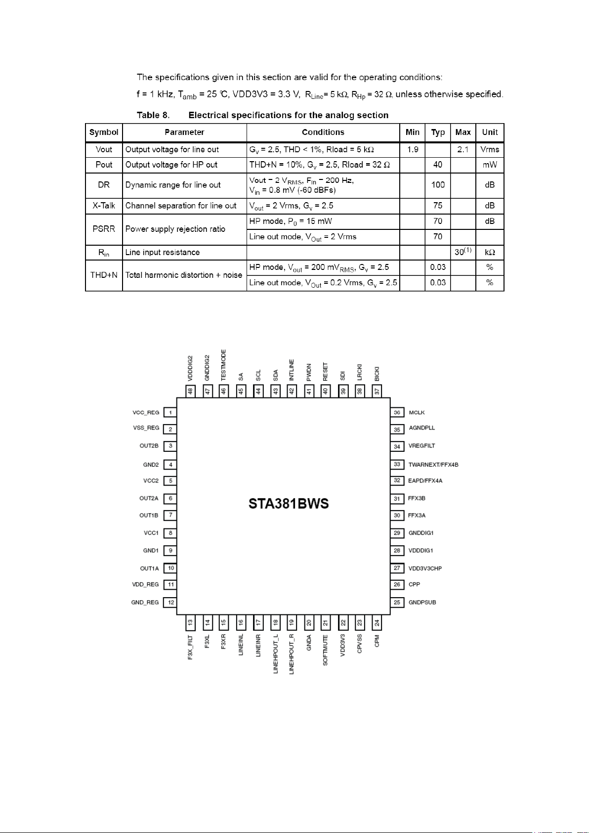
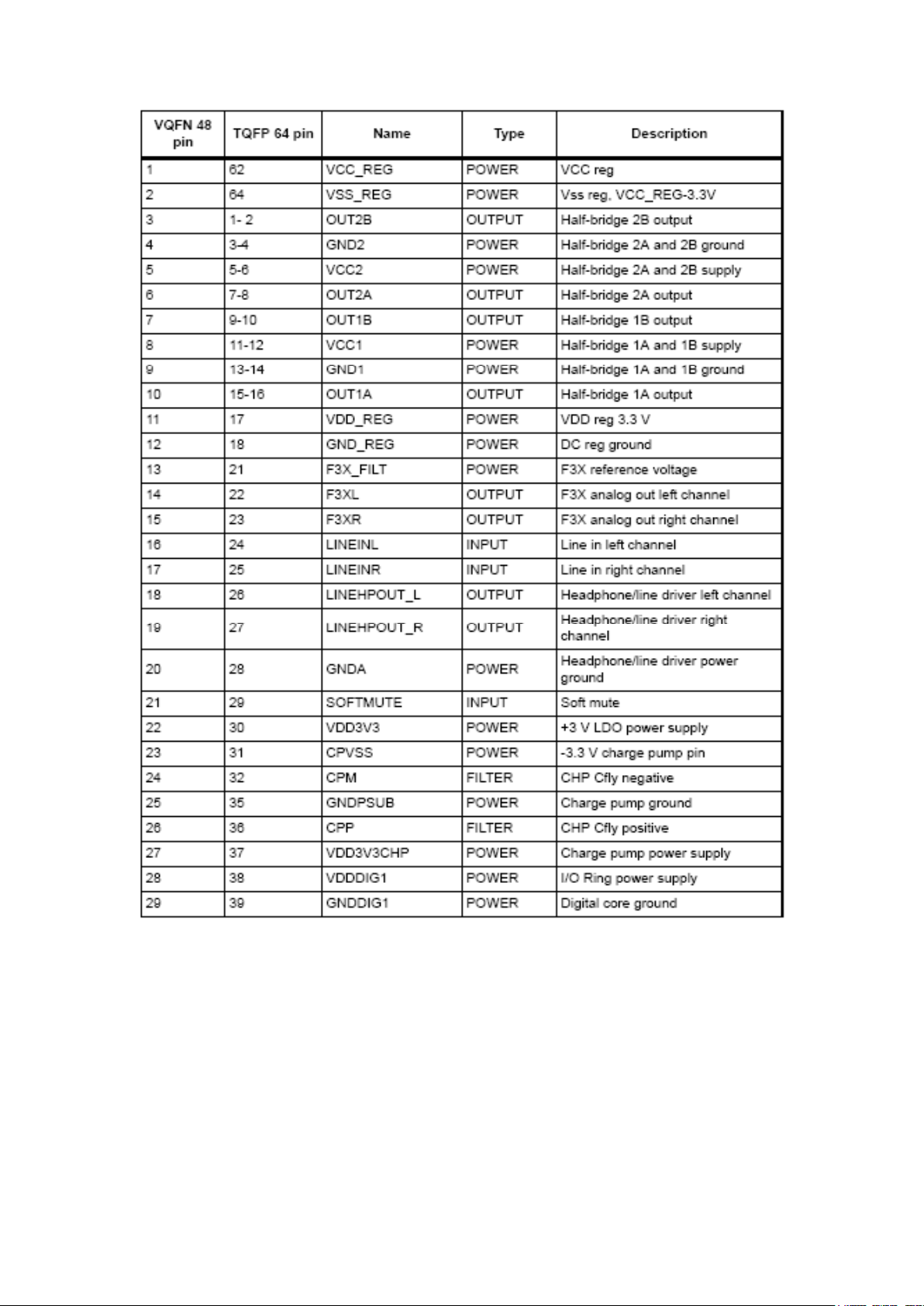
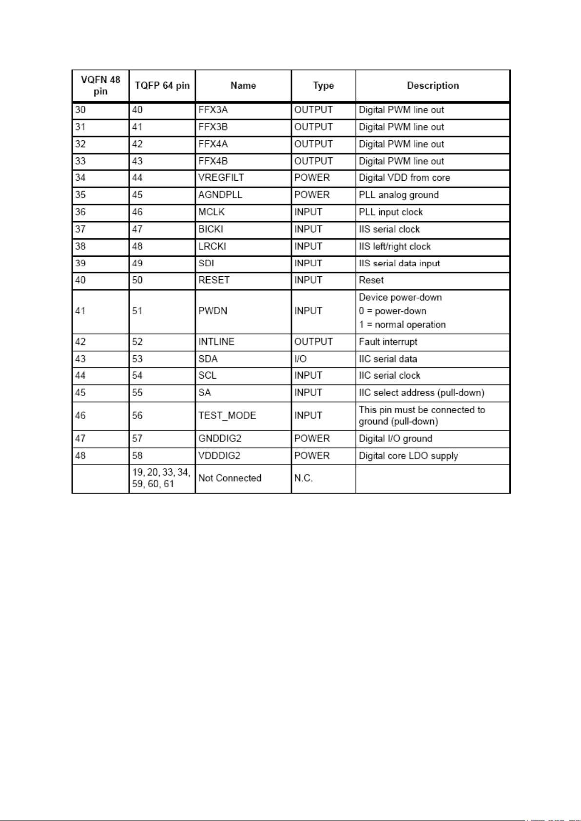
2.4. Pinning
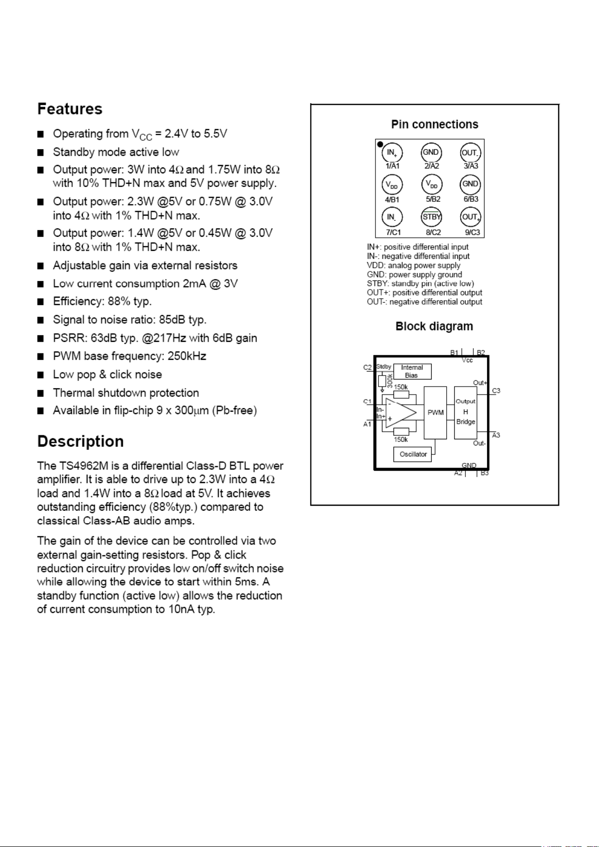
TS4962M (Optional 2,5W)

3. POWER STAGE
The DC voltages required at various parts of the chassis and panel are provided by a main power
supply unit. MB8
PW26, PW82-3, PW03, PW04, PW06, PW07 as main power supply and also with 12V adaptor.
Which power board can be used for board to board or cable connection?
chassis can operate with PW05, IPS60, IPS70, IPS16, IPS17, IPS19, PW25,
Board to board (BTB) :
Power Cable : PW25, PW26, PW82-3, PW03, PW04, PW06, PW07
The power supplies generate 24V, 12V, 5V, 3,3V and 12V, 5V,3.3V stand by mode DC voltages.
Power stage which is on-chassis generates 5V, 3V3 stand by voltage and 12V, 8V, 5V, 3V3, 2.5V,
1,8V and 1,2V supplies for other different parts of the chassis. Chassis block diagram is indicated
below.
The blocks on power block diagram is using dependent to main supply. For PW26 and PW27 just
common blocks are enough for proper operation.
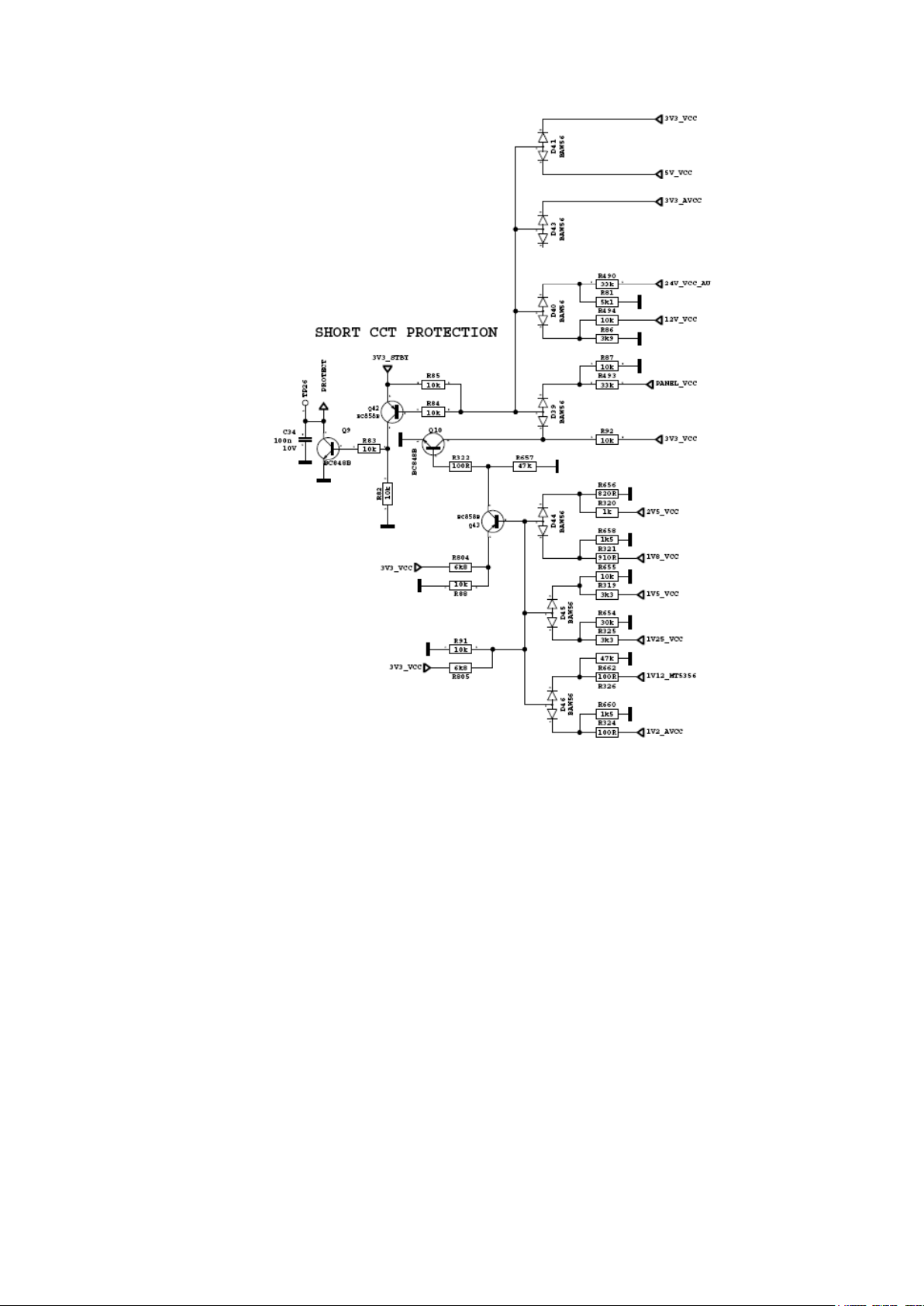
Short CCT Protection Circuit
Short circuit protection is necessary for protecting chassis and main IC against damages when any
Vcc supply shorts to ground. Protect pin should be logic high while normal operation. When there is a
short circuit protect pin shold be logic low. After any short detection, SW forces LEDs on LED card to
blink.
PW05, IPS60, IPS70, IPS16, IPS17, IPS19
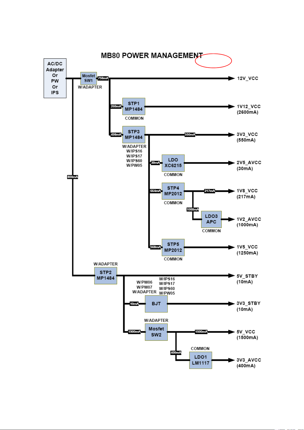
3.1. Power Management

4. MICROCONTROLLER MediaTek
4.1. Description
MT5365 (Main IC) (U1)
This document is mainly for audio quality (AQ) tuning and customization. We will introduce each AQ
module enclosed in the red box of the following audio block diagram one by one in chapter 3. We will
also include each module
customization methods.
Before we go through each module introduction, we will briefly introduce the tuning and customization
tools in the chapter 2.
Followed by chapter 3, we will include a Full-Watt manipulation example in chapter 4 that you can
start your first AQ tuning exercise.
s control CLI and tuning tool with corresponding firmware and Flash AQ


4.2. MediaTek Block Diagram

4.3. Reset Circuit
Reset circuit using for initiliazing main MediaTek IC. Reset condition is high and nomal working
condition is low for RESET pin.
5. CI INTERFACE
CI Interface Power Switch:
It is used for CI module supply, when Module is inserted (it means CI detect is low) This circuit is
opened or closed by CI_POWER_CTRL port of main uController

6. USB INTERFACE
is used for USB connectivity for last user. Last user can play video, picture and audio files.
Main Concept IC has integrated USB 2.0 interface.
Also digital channels can be record to externall storage device by this interface. All SW files can be
updated with interface.
USB circuit has 3 main parts
Integrated USB 2.0 Host interface of D3K
Protection IC
Over Curent Protection IC
7. DDR3 SDRAM NTC-DDR3-1Gb-D-R12
Description:
The 1Gb Double-Data-Rate-3 (DDR3/L) B-die DRAMs is double data rate architecture to achieve high-speed
operation. It is internally configured as an eight bank DRAM.
The 1Gb chip is organized as 16Mbit x 8 I/Os x 8 banks or 8Mbit x 16 I/Os x 8 bank devices. These
synchronous devices achieve high speed double-data-rate transfer rates of up to 2133 Mb/sec/pin for general
applications.
The chip is designed to comply with all key DDR3/L DRAM key features and all of the control and address
inputs are synchronized with a pair of externally supplied differential clocks. Inputs are latched at the cross
point of differential clocks (CK rising and
differential DQS pair in a source synchronous fashion.
These devices operate with a single 1.5V ± 0.075V &1.35V -0.067/+0.1V power supply and are available in
BGA packages.
___falling). All I/Os are synchronized with a single ended DQS or

Features:
Pinning 78 balls BGA Package (x8):

Pinning 78 balls BGA Package (x8):

8. SCALER AND LVDS SOCKETS
8.1. LVDS sockets Block Diagram

8.2. Panel Supply Switch Circuit
This switch is used to open and close panel supply of TCON. It is controlled by port of main
ucontroller. Also with this circit panel sequency could be adjusted correctly. 3 panel supplys are
connected to this circuit. All of them are optional according to panels.
9. NAND FLASH MEMORY K9F1G08U0D
9.1. General Description
Offered in 128Mx8bit, the K9F1G08X0D is a 1G-bit NAND Flash Memory with spare 32M-bit. Its
NAND cell provides the most costeffective solution for the solid state application market. A program
operation can be performed in typical 250
performed in typical 2ms on a (128K+4K)Byte block. Data in the data register can be read out at 30ns
cycle time per Byte. The I/O pins serve as the ports for address and data input/output as well as
command input. The onchip write controller automates all program and erase functions including
pulse repetition, where required, and internal verification and margining of data. Even the writeintensive systems can take advantage of the K9F1G08X0D
ECC(Error Correcting Code) with real time mapping-out algorithm. The K9F1G08X0D is an optimum
solution for large nonvolatile storage applications such as solid state file storage and other portable
app.lications requiring non-volatility.
s on the (2K+64)Byte page and an erase operation can be
s extended reliability by providing

9.2. Features
9.3. Pinning

10. I-LM1117/LM 800mA Low-Dropout Linear Regulator
The LM1117 is a series of low dropout voltage regulators with a dropout of 1.2V at 800mA of load current. It
has the same pin-out as National Semiconductors industry standard LM317.
The LM1117 is available in an adjustable version, which can set the output voltage from 1.25V to 13.8V with
only two external resistors. In addition, it is also available in five fixed voltages, 1.8V, 2.5V, 2.85V, 3.3V, and
5V. The LM1117 offers current limiting and thermal shutdown. Its circuit includes a zener trimmed bandgap
reference to assure output voltage accu
220, and TO-252 D-PAK packages. A minimum of 10 F tantalum capacitor is required at the output to improve
the transient response and stability.
Features
Available in 1.8V, 2.5V, 2.85V, 3.3V, 5V, and Adjustable
Versions
-- Space Saving SOT-223 Package
-- Current Limiting and Thermal Protection
-- Output Current 800mA
-- Line Regulation 0.2% (Max)
-- Load Regulation 0.4% (Max)
-- Temperature Range
LM1117 0°C to 125°C
LM1117I
40°C to 125°C
racy to within ±1%. The LM1117 series is available in SOT-223, TO-
Applications
n 2.85V Model for SCSI-2 Active Termination
n Post Regulator for Switching DC/DC Converter
n High Efficiency Linear Regulators
n Battery Charger
n Battery Powered Instrumentation

11. CONNECTORS
11.1. SCART (SC1)
11.2. HDMI (CN707,CN708)

11.3. VGA (CN711)

12. SERVICE MENU SETTINGS
In order to reach service menu, First Press
which is
In first screen following items can be seen:
4725.
MENU Then press the remote control code two times,

12.1. Video Settings

12.2. Audio Settings

12.3. Options
Options-1

Options-2

12.4. Tuning Settings

12.5. Source Settings

12.6. Diagnostic

12.7. USB Operations
USB operations option can not be used directly. It can be used for updating panel tool, hw
congiguration etc.
13. SOFTWARE UPDATE
In MB8 project there is only one software. From following steps software update procedure can be
seen:
1. MB8
2. Put flash memory to the tv when tv is powered off.
3. Power on the and pree OK button on the remote control when the tv is opened.
4. If First Time Installition screen comes, it means software update procedure is succesful.
.bin directly inside of a flash memory(not in a folder).
14. TROUBLESHOOTING
14.1. No Backlight Problem
Problem: If TV is working, led is normal and there is no picture and backlight on the panel.
Possible couses: Backlight pin, dimming pin, backlight supply, stby on/off pin
Backlight pin should be high in open position. If it is low, please check Q181 and panel cables.
Dimming pin should be high or square wave in open position. If it is low, please check S16 for Mstar
side and panel or power cables, connectors.

Backlight power supply should be in panel specs. Please check CN705 for MB8 , related connectors
for power supply cards.
STBY_ON/OFF should be low for standby on condition, please check R1677.

14.2. CI Module Problem
Problem: CI is not working when CI module inserted.
Possible couses: Supply, suply control pin, detect pins, mechanical positions of pins
CI supply shoul be 5V when CI module inserted. If it is not 5V please check CI_POWER_CTRL, this
pin should be low.
Please check mechanical positions of CI module.
Detect ports should be low. If it is not low please check CI connector pins, CI module pins and
3V3_VCC on MB8
.

14.3. Led Blinking Problem
Problem: LED blinking, no other operation
This problem indicates a short on Vcc voltages. Protect pin should be logic high while normal
operation. When there is a short circuit protect pin will be logic low. If you detect logic low on protect
pin, unplug the TV set and control voltage points with a multimeter to find the shorted voltage to
ground.

14.4. IR Problem
Problem: LED or IR not working
Check LED card supply on MB8
chasis.

14.5. Keypad Touchpad Problems
Problem: Keypad or Touchpad is not working
Check keypad supply and KEYBOARD pin on MB8
.
14.6. USB Problems
Problem: USB is not working or no USB Detection.
Check USB Supply, It should be nearly 5V.

14.7. No Sound Problem
Problem: No audio at main TV speaker outputs.
Check supply voltages of VDD_AUDIO, 5V_VCC and 3V3_VCC with a voltage-meter.
There may be a problem in headphone connector or headphone detect circuit (when headphone is
connected, speakers are automatically muted). Measure voltage at HP_DETECT pin, it should be
3.3v.
14.8. No Sound Problem at Headphone
Problem: No audio at headphone output.
Check HP detect pin, when headphone is. Check 5V_VCC and 3V3_VCC with a voltage-meter.
14.9. Standby On/Off Problem
Problem:
Device cannot boot, TV hangs in standby mode.


 Loading...