

Page 1
Page 2

TABLE OF CONTENTS
1. INTRODUCTION...................................................................................................................... 5
1.1. General Block Diagram.................................................................................................. 6
1.2. MB60 Placement of Blocks............................................................................................ 7
1. TUNER(TU102)......................................................................................................................... 8
1.1. General description of Samsung DTOS403LH122X:.................................................... 8
1.2. Features of DTOS403LH122X: ..................................................................................... 8
1.3. Pinning: .......................................................................................................................... 9
2. SAW FILTER – Audio – Epcos K9656M(Z101) ...................................................................... 9
2.1. Standart........................................................................................................................... 9
2.2. Features ........................................................................................................................ 10
2.3. Pin configuration .......................................................................................................... 10
2.4. Frequency response ...................................................................................................... 10
3. SAW FILTER – Video – Epcos K3958M(Z102) .................................................................... 11
3.1. Standart......................................................................................................................... 11
3.2. Features ........................................................................................................................ 11
3.3. Frequency response ...................................................................................................... 12
4. AUDIO AMPLIFIER STAGE WITH AZAD2102(U163, U164) ........................................... 12
4.1. General Description...................................................................................................... 12
4.2. Features ........................................................................................................................ 13
4.3. Absolute Ratings .......................................................................................................... 14
4.3.1. Electrical Characteristics.......................................................................................... 14
4.3.2. Operating Specifications .......................................................................................... 15
4.4. Pinning ......................................................................................................................... 16
5. AUDIO AMPLIFIER STAGE WITH TPA3113(U168) ......................................................... 16
5.1. General Description...................................................................................................... 16
5.2. Features ........................................................................................................................ 17
5.3. Absolute Ratings .......................................................................................................... 17
5.3.1. Electrical Characteristics.......................................................................................... 17
5.3.2. Operating Specifications .......................................................................................... 18
5.4. Pinning ......................................................................................................................... 18
6. POWER STAGE ...................................................................................................................... 19
6.1. Power Management...................................................................................................... 22
7. MICROCONTROLLER – MSTAR(U157) ............................................................................. 23
7.1. General Descripction.................................................................................................... 23
7.2. General Features........................................................................................................... 24
7.3. MSTAR Block Diagram............................................................................................... 28
7.4. Reset Circuit................................................................................................................. 29
8. CI INTERFACE....................................................................................................................... 29
7.1 Block Diagram ............................................................................................................. 29
7.1 CI Interface Power Switch ........................................................................................... 30
9. T2 Demodulator CXD2820R (U167)....................................................................................... 30
9.1. General Description...................................................................................................... 30
9.2. Features ........................................................................................................................ 30
9.3. Pinning ......................................................................................................................... 32
10. USB INTERFACE ............................................................................................................... 35
11. DDR2 SDRAM 8M × 4 BANKS × 16 BIT (W9751G6JB) (U154, U155) ......................... 35
11.1. General Description...................................................................................................... 35
11.2. Features ........................................................................................................................ 36
Page 3

11.3. Electrical Characteristics.............................................................................................. 36
11.4. Pinning ......................................................................................................................... 37
12. SCALER AND LVDS SOCKETS....................................................................................... 39
12.1. LVDS sockets Block Diagram ..................................................................................... 39
12.2. Panel Supply Switch Circuit ........................................................................................ 39
13. NAND FLASH MEMORY - MX25L1005 (U158) ............................................................. 40
13.1. General Description...................................................................................................... 40
13.2. Features ........................................................................................................................ 40
13.3. Absolute Maximum Ratings......................................................................................... 41
13.4. Pinning ......................................................................................................................... 41
14. NAND FLASH MEMORY – NAND512XXA2C (U162) .................................................. 42
14.1. General Description...................................................................................................... 42
14.2. Features ........................................................................................................................ 42
14.3. Pinning ......................................................................................................................... 43
15. USB2.0 to Fast Ethernet – ASIX AX88X72A (U171) ........................................................ 44
15.1. General Description...................................................................................................... 44
15.2. Features ........................................................................................................................ 44
15.3. Block Diagram ............................................................................................................. 45
15.4. Pinning ......................................................................................................................... 46
16. LM1117(U175, U180, U181)............................................................................................... 46
16.1. General Description...................................................................................................... 46
16.2. Features ........................................................................................................................ 46
16.3. Applications ................................................................................................................. 47
16.4. Absolute Maximum Ratings......................................................................................... 47
16.5. Pinning ......................................................................................................................... 47
17. MP2012 (U176).................................................................................................................... 47
17.1. General Description...................................................................................................... 47
17.2. Features ........................................................................................................................ 47
17.3. Pinning ......................................................................................................................... 48
18. RTA8283A (U23, U173)...................................................................................................... 48
18.1. General Description...................................................................................................... 48
18.2. Features ........................................................................................................................ 49
18.3. Pinning ......................................................................................................................... 49
19. MP1583 (U174).................................................................................................................... 49
19.1. General Description...................................................................................................... 49
19.2. Features ........................................................................................................................ 50
19.3. Pinning ......................................................................................................................... 50
20. FDC642 ................................................................................................................................ 51
20.1. General Description...................................................................................................... 51
20.2. Features ........................................................................................................................ 51
20.3. Pinning ......................................................................................................................... 51
21. FDC604P.............................................................................................................................. 51
21.1. General Description...................................................................................................... 51
21.2. Features ........................................................................................................................ 51
21.3. Pinning ......................................................................................................................... 52
22. CONNECTORS ................................................................................................................... 52
22.1. SCART (SC1) .............................................................................................................. 52
22.2. HDMI (CN707,CN708) ............................................................................................... 52
22.3. VGA (CN132) .............................................................................................................. 53
Page 4

23. SERVICE MENU SETTINGS............................................................................................. 54
23.1. Video Settings .............................................................................................................. 55
23.2. Audio Settings .............................................................................................................. 56
23.3. Options ......................................................................................................................... 57
23.4. Tuning Settings ............................................................................................................ 59
23.5. Source Settings............................................................................................................. 60
23.6. Diagnostic..................................................................................................................... 61
23.7. USB Operations............................................................................................................ 61
24. SOFTWARE UPDATE........................................................................................................ 62
25. TROUBLESHOOTING ....................................................................................................... 63
25.1. No Backlight Problem.................................................................................................. 63
25.2. CI Module Problem...................................................................................................... 64
25.3. Led Blinking Problem .................................................................................................. 66
25.4. IR Problem ................................................................................................................... 67
25.5. Keypad Touchpad Problems ........................................................................................ 67
25.6. USB Problems .............................................................................................................. 68
25.7. No Sound Problem ....................................................................................................... 69
25.8. No Sound Problem at Headphone ................................................................................ 69
25.9. Standby On/Off Problem.............................................................................................. 70
DVD Problems ......................................................................................................................... 70
25.10. No Signal Problem ................................................................................................... 71
Page 5

1. INTRODUCTION
17MB60 mainboard is driven by MStar SOC. This IC is capable of handling Video and
audio processing, Scaling-Display processing, 3D comb filter, OSD and text processing,
LVDS transmitting, channel and MPEG2/4 decoding, integrated DVB-T/C demodulator
and media center functionality.
TV supports PAL, SECAM, NTSC colour standards and multiple transmission standards
as B/G, D/K, I/I’, and L/L’ including German and NICAM stereo. Also DVB T, DVB-C are
supported internal demoulators of Mstar IC and DVB-T2 is supported with externall
demodulator.
Sound system output is supplying max. 2x2,5W ( less 10%THD at max output) with 4
speakers or 2x6W for stereo 8Ω speakers.
Supported peripherals are:
1 RF input VHF I, VHF III, UHF @ 75Ohm(Common)
1 Side AV (CVBS, R/L_Audio)
1 SCART socket(Common)
1 YPbPr (Optional)
1 PC input(Common)
2 HDMI 1.3 input(1 HDMI input is common, 1 input is optional)
1 S/PDIF output(Optional)
1 Headphone(Optional)
1 Common interface(Common)
1 USB(Common)
1 DVD(Optional)
1 iPod(Optional)
1 On-board Keypad(Optional)
1 External Keypad(Optional)
1 External TouchPad(Optional)
Ω
Page 6
1.1. General Block Diagram
Page 7
1.2. MB60 Placement of Blocks
(U171)
External
Keyboard
Touchboard
DVD
Connector
CI Connector
Power Connector
Nand
Flash
(U162)
Connectors
DDR2
RAM
(U154)
LVDS
USB
Saw
Filters
Main IC
(U157)
DDR2
RAM
(U155)
SPI
Flash
Ethernet
IC
Keypad
Tuner(TU102)
HDMI
Connectors
Ethernet
Connector or
Adapter DC
Input
YPbPr SAV HP
SCART
Connector
VGA
SPDIF
Out
Speaker
Con.
Led
Con
Inv.
Con
Page 8
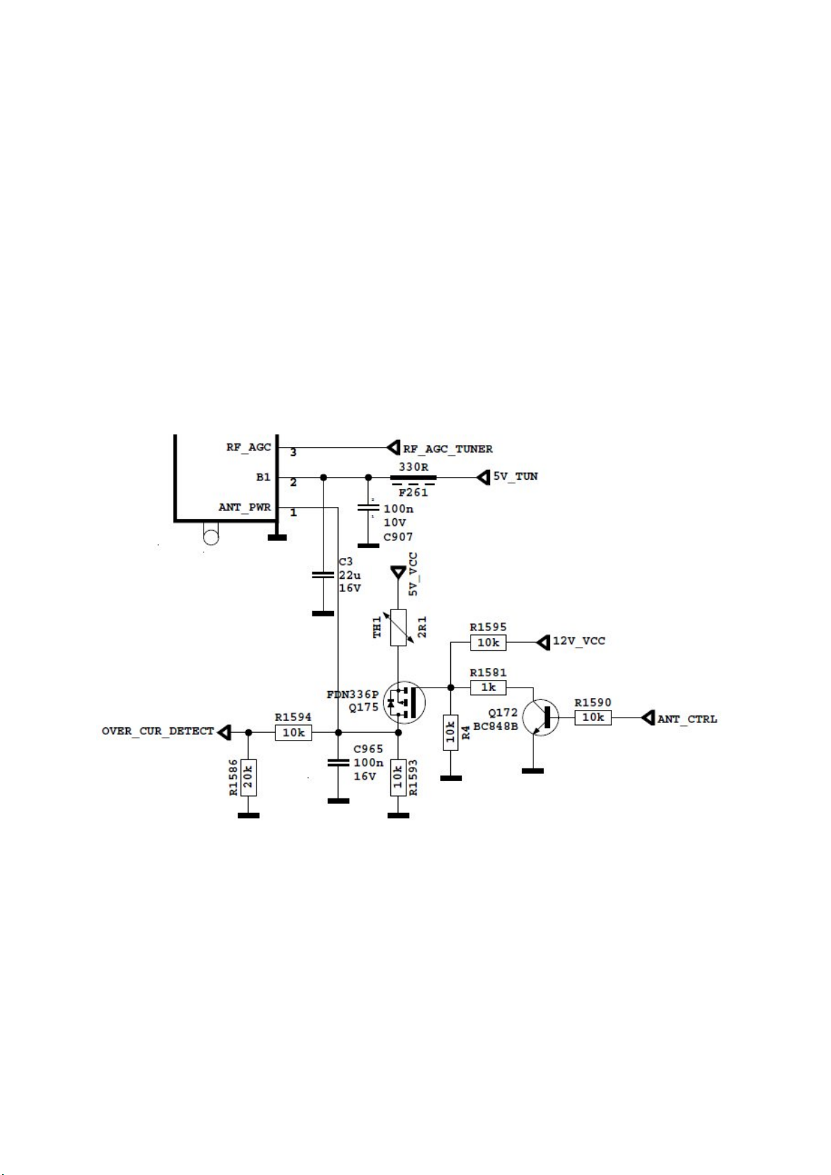
1. TUNER(TU102)
A horizontal mounted and Digital Half-Nim tuner is used in the product, which covers 3
Bands(From 48MHz to 862MHz for COFDM, from 45.25MHz to 863.25MHz for CCIR CH).
The tuning is available through the digitally controlled I2C bus (PLL). Below you will find
info about the tuner.
In active antenna option, the following circuit are used. ANT_CTRL pin is controlled by
microcontroller. If ANT_CTRL is low, ANT_PWR will be low. If ANT_CTRL is high,
ANT_PWR will be high.
OVER_CUR_DETECT pin is a monitor for short circuit in antenna. OVER_CUR_DETECT
is low, ANT_CTRL will be low, so ANT_PWR will be low. Finally, short circuit protection is
done by circuits and microcontroller.
1.1. General description of Samsung DTOS403LH122X:
The Tuner covers 3 Bands(from 48MHz to 862MHz for COFDM, from 45.25MHz to
863.25MHz for CCIR CH). Band selection and Tuning are performed digitally via the I2C
bus.
1.2. Features of DTOS403LH122X:
Receiving System: This TUNER is designed to cover the air channels in VHF and
UHF, compliant with DVB-T standard. and It covers all Analog channels from
48.25MHz to 863.25MHz
Page 9

Receiving Channel (Digital, Center frequency):
Pin n
o.
Name
Pin Description
1
Ant Power
Active Antenna Power
3
RF AGC
RF AGC (internal or external mode)
4CLI2C Serial Clock
6BP+5V, Supply Voltage (RF Amp, PLL, IF Amp)
7
BT(T.P)
+33V, within DC/DC circuit
8ASI2C Address Selection of the PLL
9
IF AGC
Control voltage for the IF AGC
11
IF OUT
-
Output 1 of the IF Amplifier
VHF Low CH. E2 ~ S10 ( 50.5MHz ~ 170.5MHz )
VHF High CH. E5 ~ S41 ( 177.5MHz ~ 466 MHz )
UHF CH. E21 ~ E69 ( 474 MHz ~ 858 MHz )
Receiving Channel (PAL, Picture carrier frequency):
VHF Low CH. E2 ~ S10 ( 48.25MHz ~ 168.25MHz )
VHF High CH. E5 ~ S41 ( 175.25MHz ~ 463.25MHz )
UHF CH. E21 ~ E70 ( 471.25MHz ~ 863.25MHz )
Intermediate Frequency:
Digital(center) DVB-T (36.167 MHz)
Digital(center) DVB-C (36.125 MHz)
Analog(picture) 38.9 MHz
Input Impedance: 75Ω, Unbalanced
Band Change-Over System
PLL Control System
Tuning System
Electronic Tuning System With PLL
Internal(or External) RF AGC function
Built in wideband AGC detector with 6 programmable take-over points
1.3. Pinning:
Terminal
2 B+ +5V, Supply Voltage (Preamplifier, DC/DC)
5 DA I2C Serial Clock
10 IF OUT + Output 2 of the IF Amplifier
12 AIF Output IF output of the Analog BroadBand
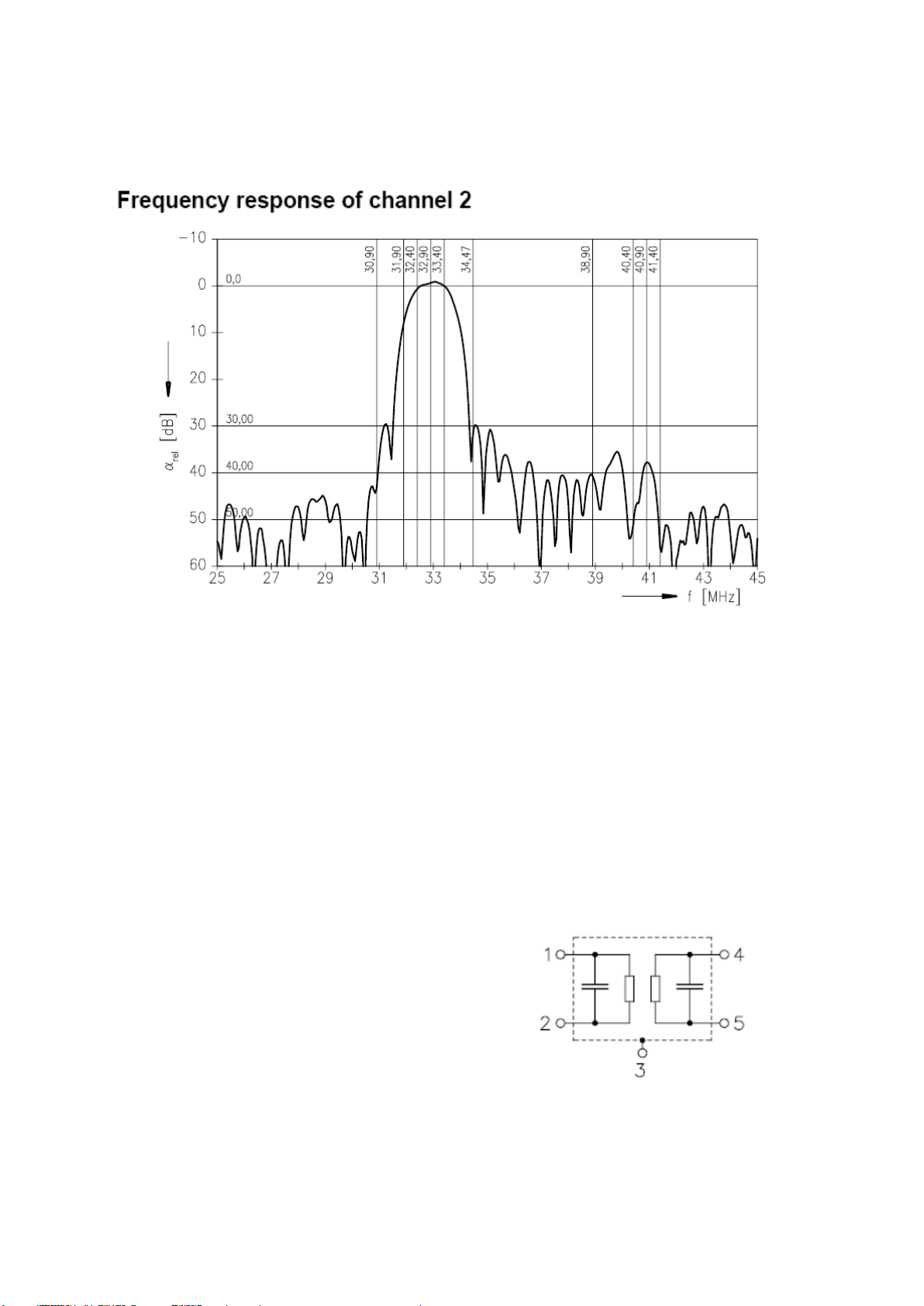
2. SAW FILTER – Audio – Epcos K9656M(Z101)
2.1. Standart
B/G
D/K
I
L/L’
Page 10
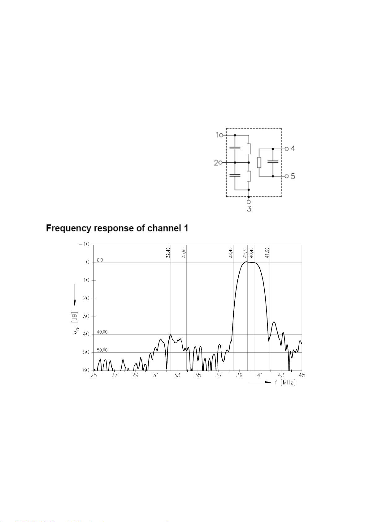
2.2. Features
TV IF audio filter with two channels
Channel 1 (L’) with one pass band for sound carriers at 40,40 MHz (L’) and 39,75
MHz (L’- NICAM)
Channel 2 (B/G,D/K,L,I) with one pass band for sound carriers between 32,35 MHz
and 33,40 MHz
2.3. Pin configuration
1 Input
2 Switching input
3 Chip carrier - ground
4 Output
5 Output
2.4. Frequency response
Page 11
3. SAW FILTER – Video – Epcos K3958M(Z102)
3.1. Standart
B/G
D/K
I
L/L’
3.2. Features
TV IF filter with Nyquist slopes at 33.90 MHz and 38.90 MHz
Constant group delay
Pin configuration:
1 Input
2 Input - ground
3 Chip - carrier ground
4 Output
5 Output
Page 12
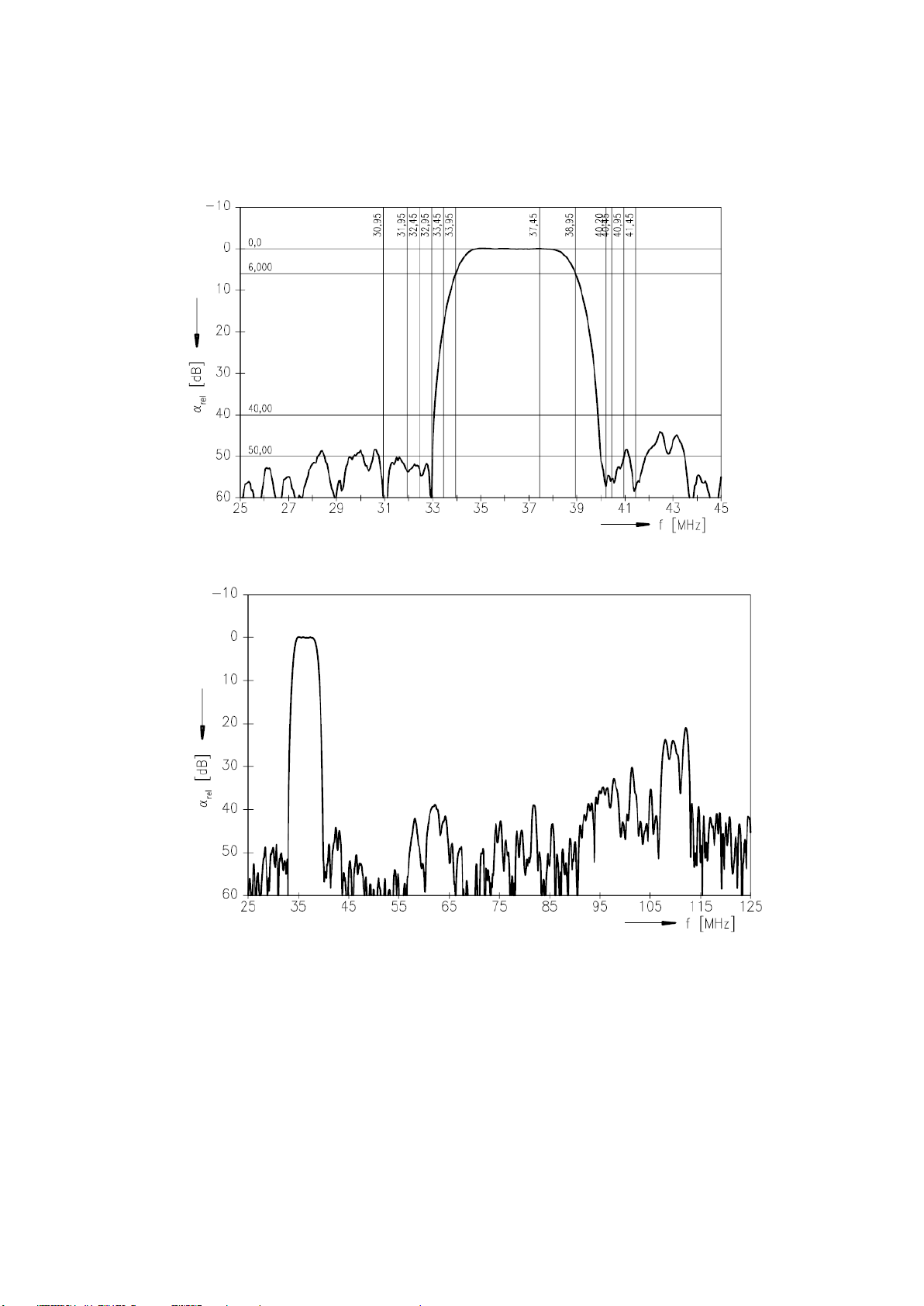
3.3. Frequency response
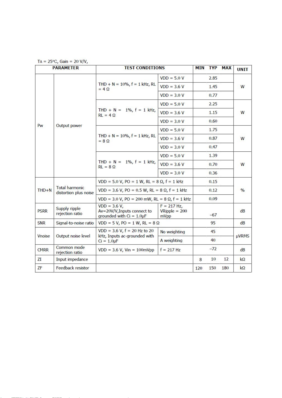
4. AUDIO AMPLIFIER STAGE WITH AZAD2102(U163, U164)
4.1. General Description
17MB60 uses two 2,5W Class D Mono Audio Amplifers for from 16” to 24” TVs.
AZAD2102B is a 2.9 Watts (max. can offer 3.0 Watts @ Load = 3Ω,THD=10%,
AVdd=DVdd=5.5Volt)with high efficiency filter-free class-D audio power amplifier in a
1613 mm x 1613 mm wafer chip scale package (WCSP). AZAD2102B uses Currentswitch technology to achieve high performance class-d amplifier that features 0.03%
THD, 85% efficiency, –70 dB PSRR, to improve RF-rectification immunity.
Page 13

AZAD2102B provide a Vibration-Spectrum modulation clock for PWM Output. This
vibration frequency is around 10KHZ shift (+/- 5KHZ of Fpwm).
The advantage of the small size package (WCSP) makes AZAD2102B very suitable for
mobile phone and PDA device application. And the Class-D amplifier structure let
AZAD2102B to have highly efficiency power consumption than Class-AB amplifier.
AZAD2102B can shrink the application board, reduce system cost, and external
components.
ESD level protection I/O embedded in AZAD2102B. For general applications, doesn’t
need to add extra ESD protection device (like Varistors) in application system for
AZAD2102B’s I/O.
4.2. Features
CMOS Technology
High Efficiency 85%
High PSRR 70dB at 217Hz
Differential OP-amp Input
AZAD2102B provides Vibration-Spectrum Modulation clock for reduce EMI
Provide Mute function(set Mute_B to GND will go into Mute status)
For the input stage AZAD2102B built-in a 10Kohm resistors (Gain setting=29.5dB)
Maximum Battery Life and Minimum Heat
Efficiency With an 8-Ω Speaker:
3.5 mA Quiescent Current
Output Power at 10% THD
2.85Watts at AVdd=DVdd=5.0Volt, Rload=4Ω
1.45Watts at AVdd=DVdd=3.6Volt, Rload=4Ω
0.30Watts at AVdd=DVdd=3.0Volt, Rload=4Ω
1.75Watts at AVdd=DVdd=5.5Volt, Rload=8Ω
0.87Watts at AVdd=DVdd=3.6Volt, Rload=8Ω
0.41Watts at AVdd=DVdd=3.0Volt, Rload=8Ω
Eliminate Power on and Power-off “Pop” noise
A Fewer External Components
Optimized PWM Output Stage Eliminates LC Output Filter
Internally generate 290 kHz Switching Frequency to eliminate Capacitor and
Resistor
Improve PSRR (–70 dB) and Wide Supply Voltage (3.0 V to 5.5 V)
Fully Differential Design Reduces RF Rectification
This chip has been built-in a very strong ESD protection.
System level ESD 4KV (IEC 61000-4-2 ESD Contact Level)
Wafer Chip Scale Package (WCSP)
TSSOP Package with Exposed Pad
Page 14
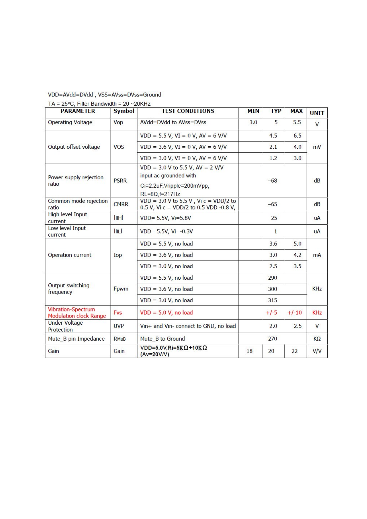
4.3. Absolute Ratings
4.3.1. Electrical Characteristics
Page 15
4.3.2. Operating Specifications
Page 16
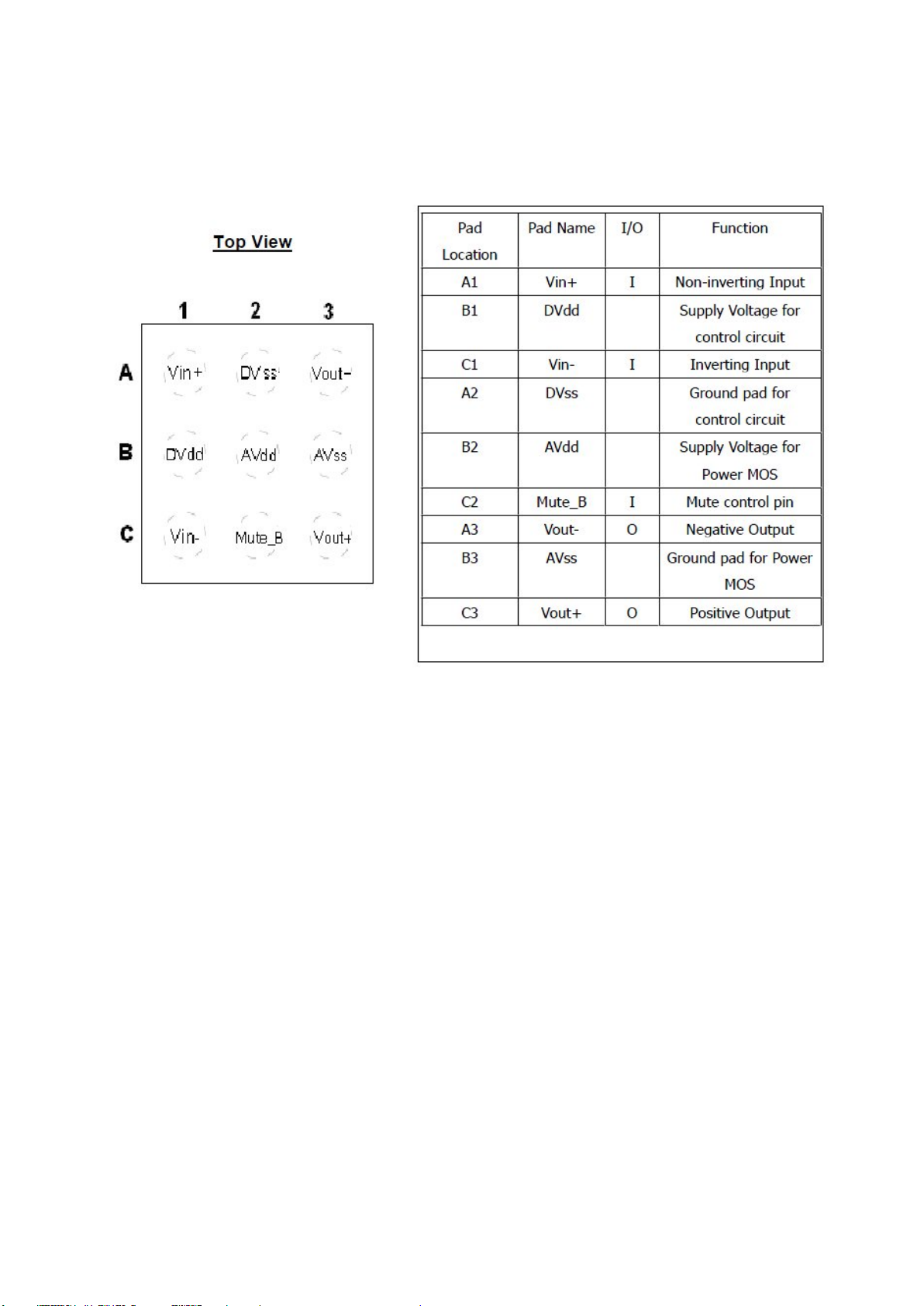
4.4. Pinning
5. AUDIO AMPLIFIER STAGE WITH TPA3113(U168)
5.1. General Description
17MB60 uses a 6W Class D Mono Audio Amplifers for from 26” to 32” TVs. The
TPA3113D2 is a 6-W (per channel) efficient, Class-D audio power amplifier for driving
bridged-tied stereo speakers. Advanced EMI Suppression Technology enables the use of
inexpensive ferrite bead filters at the outputs while meeting EMC requirements.
SpeakerGuard™ speaker protection circuitry includes an adjustable power limiter and a
DC detection circuit. The adjustable power limiter allows the user to set a "virtual" voltage
rail lower than the chip supply to limit the amount of current through the speaker. The DC
detect circuit measures the frequency and amplitude of the PWM signal and shuts off the
output stage if the input capacitors are damaged or shorts exist on the inputs.
The TPA3113D2 can drive stereo speakers as low as 4
TPA3113D2, 87%, eliminates the need for an external heat sink when
playing music.
The outputs are also fully protected against shorts to GND, VCC, and output-to-output.
The short-circuit protection and thermal protection includes an auto-recovery feature.
Ω. The high efficiency of the
Page 17
5.2. Features
6-W/ch into an 8-Ω Loads at 10% THD+N From a 10-V Supply
12-W into a 4-Ω Mono Load at 10% THD+N From a 10-V Supply
87% Efficient Class-D Operation Eliminates Need for Heat Sinks
Wide Supply Voltage Range Allows Operation from 8 V to 26 V
Filter-Free Operation
SpeakerGuard™ Speaker Protection Includes Adjustable Power Limiter plus DC
Protection
Flow Through Pin Out Facilitates Easy Board Layout
Robust Pin-to-Pin Short Circuit Protection and Thermal Protection with Auto
Recovery Option
Excellent THD+N / Pop-Free Performance
Four Selectable, Fixed Gain Settings
Differential inputs
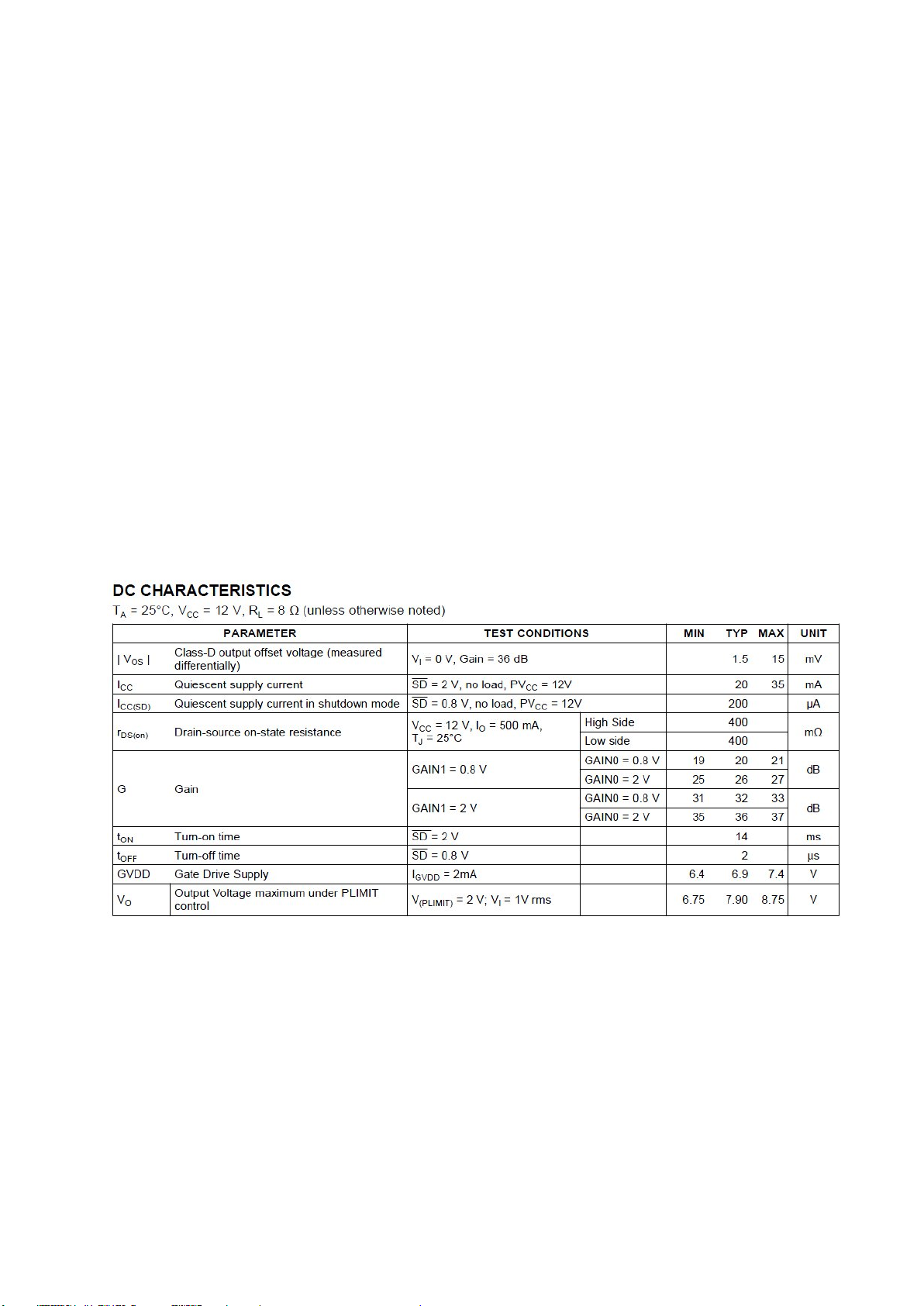
5.3. Absolute Ratings
5.3.1. Electrical Characteristics
Page 18
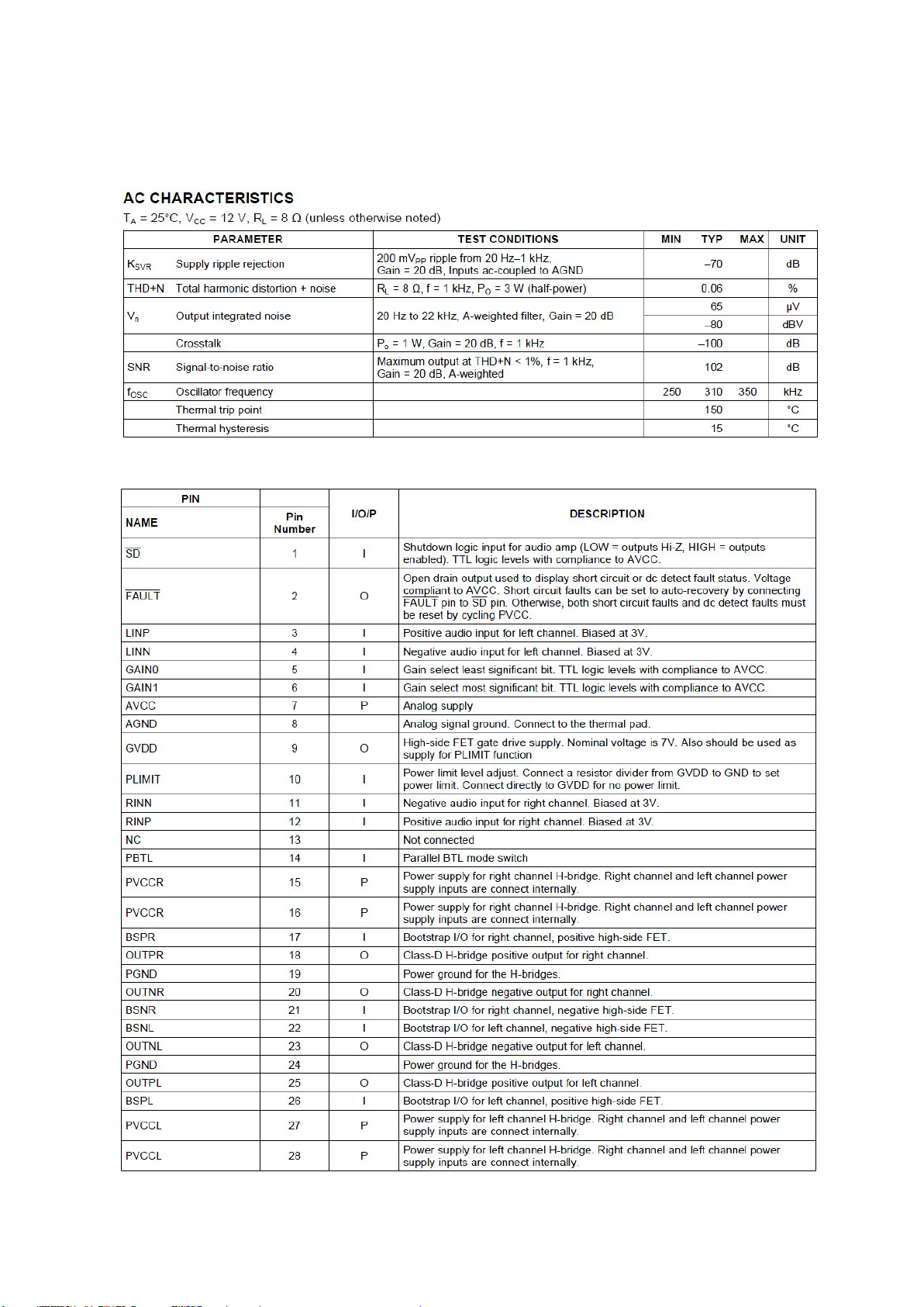
5.3.2. Operating Specifications
5.4. Pinning
Page 19
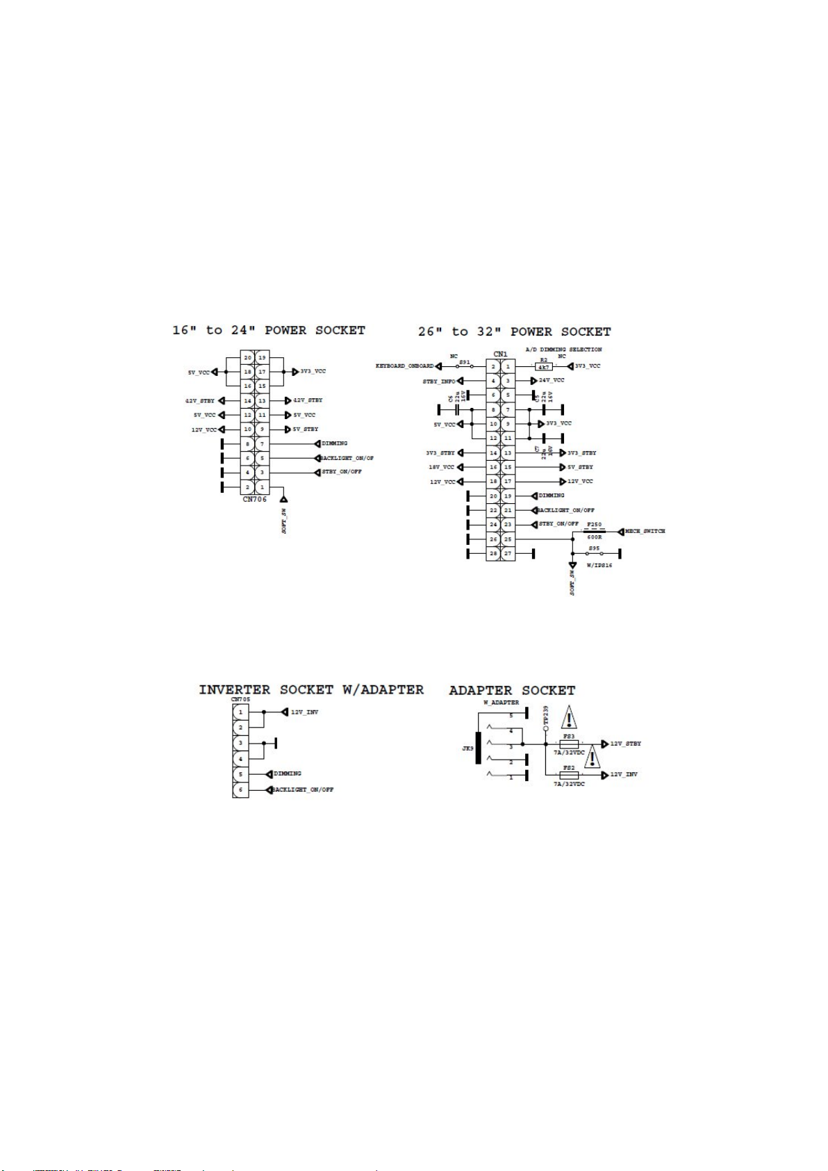
6. POWER STAGE
The DC voltages required at various parts of the chassis and panel are provided by a
main power supply unit. MB60 chassis can operate with IPS60, IPS16, IPS17, PW26,
PW27 as main power supply and also with 12V adaptor.
CN706 is used for IPS60, IPS16 and IPS17 and CN1 is used for PW26 and PW27.
JK9 is used for the adapter option and also CN705 inverter socket or DB32 chassis with
CN706 is used to supply backlight.
The power supplies generate 18V, 12V, 5V, 3,3V and 12V, 5V, stand by mode DC
voltages. Power stage which is on-chassis generates 5V, 3V3 stand by voltage and 12V,
8V, 5V, 3V3, 2.5V, 1,8V and 1,2V supplies for other different parts of the chassis. Chassis
block diagram is indicated below.
Page 20
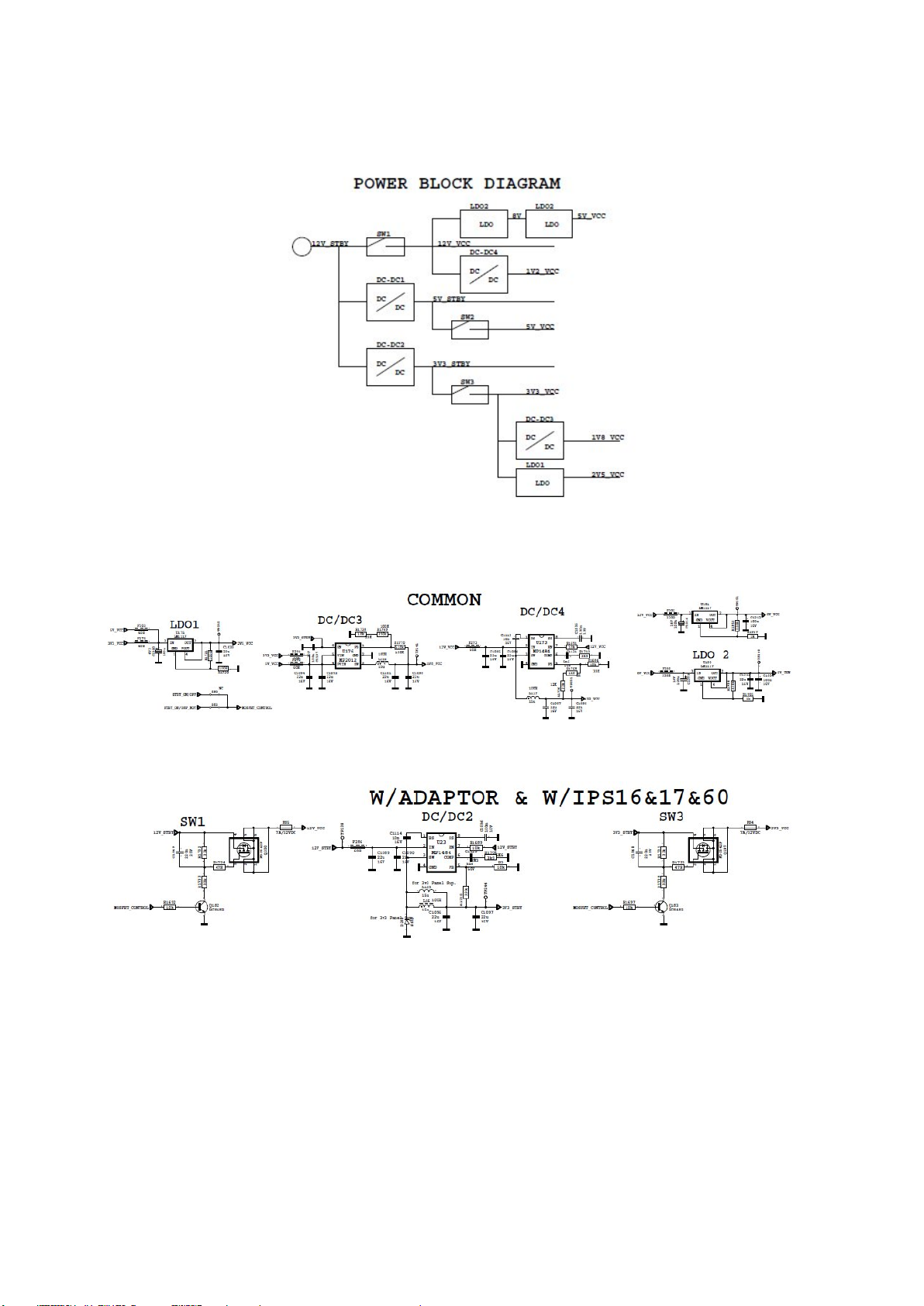
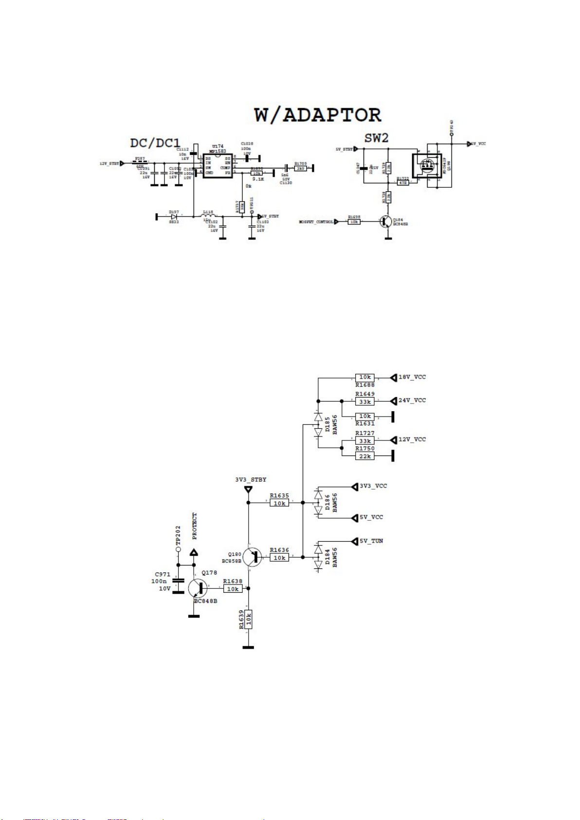
The blocks on power block diagram is using dependent to main supply. For PW26 and
PW27 just common blocks are enough for proper operation.
For IPS16, IPS17, IPS60 below blocks must work properly.
For adopter case also below blocks are necessary.
Page 21
Short CCT Protection Circuit
Short circuit protection is necessary for protecting chassis and main IC against damages
when any Vcc supply shorts to ground. Protect pin should be logic high while normal
operation. When there is a short circuit protect pin shold be logic low. After any short
detection, SW forces LEDs on LED card to blink.
Page 22
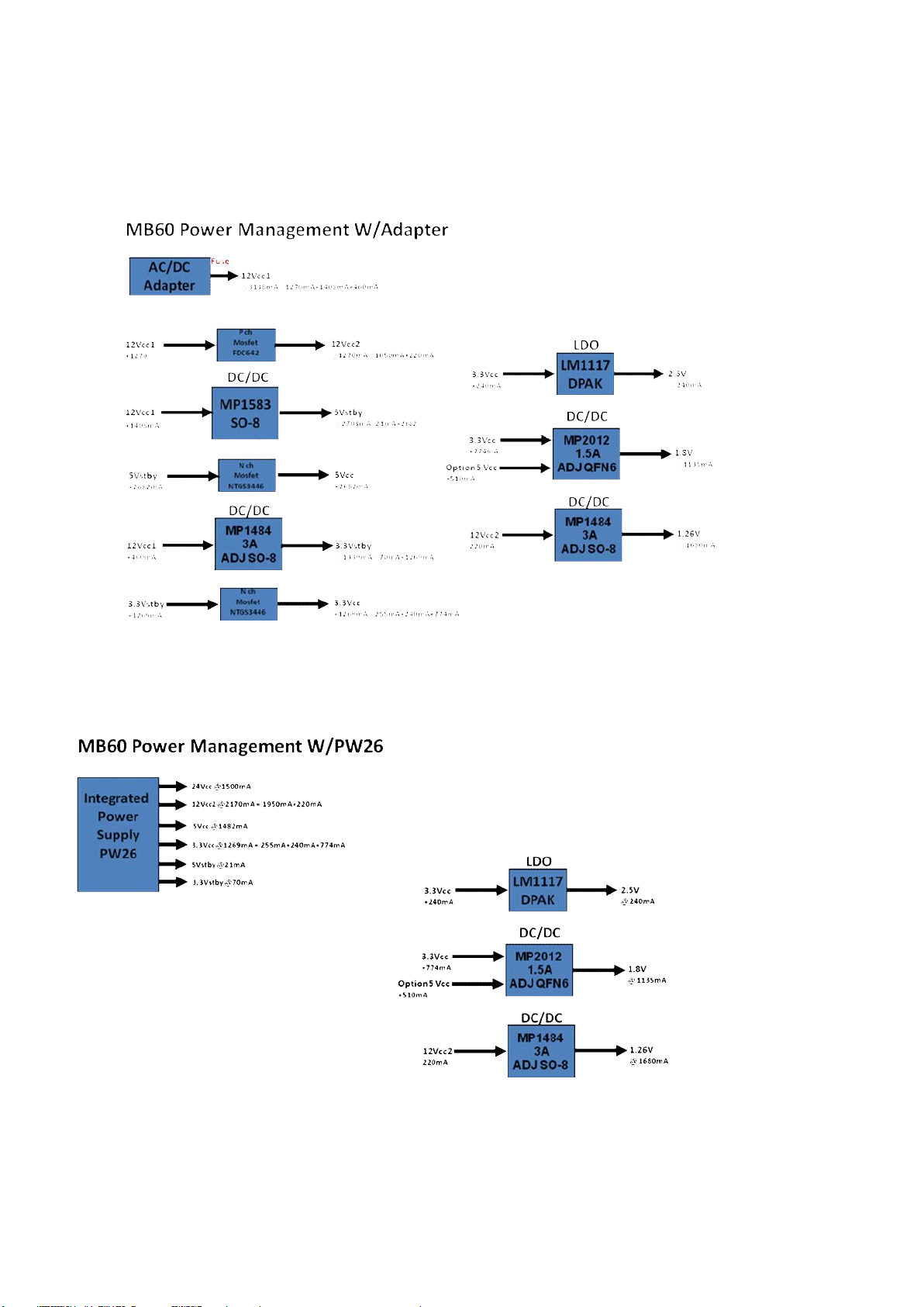
6.1. Power Management
Page 23

7. MICROCONTROLLER – MSTAR(U157)
7.1. General Descripction
The MSD9WB7PX-2 integrates DTV/multi-media all-purpose AV decoder, DVB-T
demodulator, VIF demodulator, and Sound/Video processor into a single device. This
allows the overall BOM to be reduced significantly making the MSD9WB7PX-2 a very
Page 24

competitive multi-media DTV solution. For ATV users, the MSD9WB7PX-2 provides multistandard analog TV support with adaptive 3D video decoding and VBI data extraction.
The build-in audio decoder is capable of decoding FM, AM, NICAM, A2, BTSC and EIA-J
sound standards. The MSD9WB7PX-2 supplies all the necessary A/V inputs and outputs
to complete a receiver design including a multi-port HDMI receiver and component video
ADC. All input selection multiplexed for video and audio are integrated, including full
SCART support with CVBS output. The equipped MStar MACE-5 color engine is the
latest masterpiece from MStar famous color engine series providing excellent video and
picture quality in Full-HD and large-scale displaying system. To meet the increasingly
popular energy legislative requirements without the use of additional hardware, the
MSD9WB7PX-2 has an ultra low power standby mode during which an embedded MCU
can act upon standby events and wake up the system as required.
7.2. General Features
MSD9WB9PX-2, an SOC solution that supports channel decoding, MPEG decoding, and
media-centre functionality enabled by a high performance AV CODEC and CPU Key
features include,
Digital and Analog DVB Front-End Demodulator
A Multi-Standard A/V Format Decoder
The MACE-5 Video Processor
Home Theater Sound Processor
Peripheral and Power Management
Transport Stream De-multiplexer
Supports parallel and serial TS interface, with or without sync signal
Supports TS input and output for external CI module
Maximum TS data rate is 104 Mb/sec for serial or 16 MB/sec for parallel
32 general purpose PID filters and section filters for each transport stream de-
multiplexer
Supports additional audio/video/PCR filters
Supports TS DMA channel for time-shift
Supports 3DES/DES and AES encryption/decryption
MPEG-2 Video Decoder
ISO/IEC 13818-2 MPEG-2 video MP@HL
Automatic frame rate conversion
Supports resolution up to HDTV (1080i, 720p) and SDTV
MPEG-4 Video Decoder
ISO/IEC 14496-2 MPEG-4 ASP video decoding
Supports resolutions up to HDTV (1080p@30fps)
Supports DivX1 Home Theater & HD profilesOptional
Supports VC-1Optional, FLV video format decoding
H.264 Decoder
ITU-T H.264, ISO/IEC 14496-10 (main and high profile up to level 4.1) video
decoding
Page 25

Supports resolutions for all DVB, ATSC, HDTV, DVD and VCD
Supports resolution up to 1080p@30fps
Supports CABAC and CAVLC stream types
Processing of ES and PES streams, extraction and provision of time stamps
Up to 40 Mbits bitrate (Blu-ray spec.)
Hardware JPEG
Supports sequential mode, single scan
Supports both color and grayscale pictures
Following the file header scan the hardware decoder fully handles the decode
process
Supports programmable Region of Interest (ROI)
Supports formats: 422/411/420/444/422T
Supports scaling down ratios: 1/2, 1/4, 1/8
Supports picture rotation
NTSC/PAL/SECAM Video Decoder
Supports NTSC-M, NTSC-J, NTSC-4.43, PAL (B, D, G, H, M, N, I, Nc), and
SECAM standards
Automatic standard detection
Motion adaptive 3D comb filter
Five configurable CVBS & Y/C S-video inputs
Supports Teletext, Closed Caption (analog CC 608/ analog CC 708/digital CC
608/digital CC 708), V-chip and SCTE
Multi-Standard TV Sound Processor
SIF audio decoding
Supports BTSC/A2/EIA-J demodulation
Supports NICAM/FM/AM demodulation
Supports MTS Mode Mono/Stereo/SAP in BTSC/EIA-J mode
Supports Mono/Stereo/Dual in A2/NICAM mode
Built-in audio sampling rate conversion (SRC)
Audio processing for loudspeaker channel, including volume, balance, mute, tone,
EQ, virtual stereo/surround and treble/bass controls
Advanced sound processing options available, for example: Dolby, SRS, BBE,
QSound, Audyssey
Supports digital audio format decoding:
MPEG-1, MPEG-2 (Layer I/II), MP3, Dolby Digital (AC-3), AAC-LC
Supports Optional Dolby Digital Plus, Dolby Pulse, and MS10 multistream
decoder, including Dolby Digital Encoder for transcoding streams to Dolby Digital
5.1 (DDCO)
Supports MPEG Audio, Dolby Digital, Dolby Digital Plus format AD (Audio
Description)
Supports PVR and time-shifting
Audio Interface
One SIF audio input interface with minimal external saw filters
Page 26

Four L/R audio line-inputs including Mic. input
Two L/R outputs for main speakers and additional line-outputs
Supports stereo headphone driver
I2S digital audio input & output
S/PDIF digital audio output
HDMI audio channel processing
Programmable delay for audio/video synchronization
Analog RGB Compliant Input Port
Three analog ports support up to 1080P
Supports PC RGB input up to SXGA@75Hz
Supports HDTV RGB/YPbPr/YCbCr
Supports Composite Sync and SOG Sync-on-Green
Automatic color calibration
AV-link support
Analogue RGB Auto-Configuration & Detection
Auto input signal format and mode detection
Auto-tuning function including phasing, positioning, offset, gain, and jitter detection
Sync Detection for H/V Sync
DVI/HDCP/HDMI Compliant Input Port
Three HDMI/DVI Input ports
HDMI 1.3 Compliant
HDCP 1.1 Compliant
225MHz @ 1080P 60Hz input with 12-bit Deep-color support
CEC support
Single link DVI 1.0 compliant
Robust receiver with excellent long-cable support
MStar Advanced Color Engine (MStarACE-5)
10/12-bit internal data processing
Fully programmable multi-function scaling engine
Nonlinear video scaling supports various modes including Panorama
Supports dynamic scaling for VC-1
High-Quality DTV video processor
3D motion video deinterlacer with motion object stabilizer
Edge-oriented deinterlacer with edge and artifact smoother
Automatic 3:2/2:2/M:N pull-down detection and recovery
3D multi-purpose noise reduction for DTV or lousy air/cable input
MPEG artifact removal including de-blocking and mosquito noise reduction
Arbitrary frame rate conversion
MStar Professional Picture Enhancement:
o Dynamic brilliant and fresh color
o Dynamic Blue Stretch
o Intensified contrast and details
o Dynamic Vivid Skin
Page 27

o Dynamic sharpened Luma/Chroma edges
o Global and local dynamic depth of field perception
o Accurate and independent color control
o Supports sRGB and xvYCC color processing
o Supports HDMI 1.3 deep color format
Programmable 12-bit RGB gamma CLUT
Output Interface
Single/dual link 8/10-bit LVDS output
Supports panel resolution up to Full-HD (1920x1080) @ 60Hz
Supports TH/TI format
Supports dithering options to 6/8-bit output
Spread spectrum output for EMI suppression
CVBS Video Encoder
Supports all NTSC/PAL TV Standard
Stand-alone scaling engine
Programmable Hue, Contract, Brightness
Supports TTX/CC/WSS output
CVBS Video Output
Allows CVBS output of all source inputs
2D Graphics Engine
Hardware Graphics Engine for responsive interactive applications
Supports point draw, line draw, rectangle draw/fill, text draw and trapezoid draw
BitBlt, stretch BitBlt, trapezoid BitBlt, mirror BitBlt and rotate BitBlt
Raster Operation (ROP)
Support Porter-Duff
VIF Demodulator
Compliant with NTSC M/N, PAL B, G/H, I, D/K, SECAM L/L' standards
Audio/Video dual-path processor
Stepped-gain PGA with 25 dB tuning range and 1 dB tuning resolution
Maximum IF gain of 37 dB
Programmable TOP to accommodate different tuner gain and SAW filter insertion
loss to optimize noise and linearity performance
Multi-standard processing with single SAW
Supports silicon tuner low IF output architecture
DVB-T/DVB-C Demodulator
Digital carrier frequency offset correction: ±500KHz
Optimised for SFN channels with pre/post-cursive echoes inside/outside the guard
Acquisition range ±857kHz includes up to 3x: ±1/6 MHz transmitter offset
Meets Nordig Unified 1.0.3, D-Book 5.0, EICTA E-Book/C-Book test requirement
ITU J.83 Annex A/C, DVB-C (EN 300 429) compliant
Supports DVB-C 0.7-7M Baud symbol rate
Page 28

±400kHz internal carrier offset recovery range
6.8 usecs echo cancellation at 7 Msym/s
Supports IF, low-IF, zero-IF inputs
Ultra-fast automatic blind UHF/VHF channel scan (constellations and symbol rate)
Connectivity
Two USB 2.0 host ports
USB architecture designed for efficient suppor of external storage devices in
conjunction with off air broadcasting
Miscellaneous
DRAM interface supporting two 16-bit DDR2 @ 1066MHz
Supports PVR
Supports Common Interface for conditional access support
Bootable SPI interface with serial flash support
Parallel interface for external OneNAND and NAND flash support
Power control module with ultra low power
MCU available in standby mode
523-ball LFBGA package
Operating Voltages: 1.26V (core), 1.8V (DDR2), 2.5V and 3.3V (I/O and analog)
7.3. MSTAR Block Diagram
Page 29

7.4. Reset Circuit
Reset circuit using for initiliazing main Mstar IC. Reset condition is high and nomal
working condition is low for RESET pin.
8. CI INTERFACE
7.1 Block Diagram
Page 30

7.1 CI Interface Power Switch
It is used for CI module supply, when Module is inserted (it means CI detect is low) This
circuit is opened or closed by CI_POWER_CTRL port of main uController
9. T2 Demodulator CXD2820R (U167)
9.1. General Description
This demodulator is optionall for support T2 reception. The Sony CXD2820R is a
combined DVB-T2, DVB-T and DVB-C demodulator that conforms to the ETSI EN 302755 (second generation Terrestrial) ETSI EN 300-744 (Terrestrial) and ETSI EN 300-429
(Cable) standards.
9.2. Features
Single, 41MHz crystal (can be shared with CXD2813Ranalogue demod IC)
High performance differential signal ADC
RF power level monitor ADC
Low IF and high IF (36MHz) mode input
Fast 400kHz I2C compatible bus interface
Page 31

Quiet I2C interface for dedicated tuner control
Automatic IF AGC and optional programmable
RF AGC/GPIO functions
Configurable parallel and serial MPEG-2 TS outputs with smoothing buffer
3.3V, 2.5V, 1.2V supplies
Temperature range -20°C to +85°C
Supplied with full reference design, including software driver, PCB
schematic/layouts, GUI and documentation
3.3V for VDD and 2.5V for VDDQ power supply
All inputs and outputs are compatible with SSTL_2 interface
JEDEC standard 400mil 66pin TSOP-II with 0.65mm pin pitch
Fully differential clock inputs (CK, /CK) operation
Double data rate interface
Source synchronous - data transaction aligned to bidirectional data strobe (DQS)
x16 device has 2 bytewide data strobes (LDQS, UDQS) per each x8 I/O
Data outputs on DQS edges when read (edged DQ) Data inputs on DQS centers
when write (centered DQ)
Data(DQ) and Write masks(DM) latched on the both rising and falling edges of the
data strobe
All addresses and control inputs except Data, Data strobes and Data masks
latched on the rising edges of the clock
Write mask byte controls by LDM and UDM
Programmable /CAS latency 3 / 4 supported
Programmable Burst Length 2 / 4 / 8 with both sequential and interleave mode
Internal 4 bank operations with single pulsed /RAS
tRAS Lock-Out function supported
Auto refresh and self refresh supported
4096 refresh cycles / 32ms
Full, Half and Matched Impedance(Weak) strength driver option controlled by
EMRS
Page 32

9.3. Pinning
Page 33

Page 34

Page 35

10. USB INTERFACE
Main Concept IC has integrated 2 USB 2.0 interface. One of them is used for ethernet
function, the other one is used for USB connectivity for last user. Last user can play video,
picture and audio files. Also digital channels can be record to externall storage device by
this interface. All SW files can be updated with interface.
USB circuit has 3 main parts
Integrated USB 2.0 Host interface of D3 (U157)
Protection IC (U145)
Over Curent Protection IC (U149)
11. DDR2 SDRAM 8M × 4 BANKS × 16 BIT (W9751G6JB)
(U154, U155)
11.1. General Description
The W9751G6JB is a 512M bits DDR2 SDRAM, organized as 8,388,608 words × 4 banks
× 16 bits. This device achieves high speed transfer rates up to 1066Mb/sec/pin (DDR2-
1066) for general applications. W9751G6JB is sorted into the following speed grades: -18,
-25 and -3. The -18 is compliant to the DDR2-1066/CL7 specification. The -25 is
compliant to the DDR2-800 (5-5-5) or DDR2-800 (6-6-6) specification. The -3 is compliant
to the DDR2-667 (5-5-5) specification. All of the control and address inputs are
synchronized with a pair of externally supplied differential clocks. Inputs are latched at the
cross point of differential clocks (CLK rising and CLK falling). All I/Os are synchronized
with a single ended DQS or differential DQS- DQS pair in a source synchronous fashion.
Page 36

11.2. Features
Power Supply: VDD, VDDQ = 1.8 V± 0.1 V
Double Data Rate architecture: two data transfers per clock cycle
CAS Latency: 3, 4, 5, 6 and 7
Burst Length: 4 and 8
Bi-directional, differential data strobes (DQS andDQS ) are transmitted / received
with data
Edge-aligned with Read data and center-aligned with Write data
DLL aligns DQ and DQS transitions with clock
Differential clock inputs (CLK and CLK )
Data masks (DM) for write data
Commands entered on each positive CLK edge, data and data mask are
referenced to both edges of DQS
Posted CAS programmable additive latency supported to make command and data
bus efficiency
Read Latency = Additive Latency plus CAS Latency (RL = AL + CL)
Off-Chip-Driver impedance adjustment (OCD) and On-Die-Termination (ODT) for
better signal quality
Auto-precharge operation for read and write bursts
Auto Refresh and Self Refresh modes
Precharged Power Down and Active Power Down
Write Data Mask
Write Latency = Read Latency - 1 (WL = RL - 1)
Interface: SSTL_18
11.3. Electrical Characteristics
Page 37

11.4. Pinning
Page 38

Page 39

12. SCALER AND LVDS SOCKETS
12.1. LVDS sockets Block Diagram
12.2. Panel Supply Switch Circuit
This switch is used to open and close panel supply of TCON. It is controlled by port of
main ucontroller. Also with this circit panel sequency could be adjusted correctly. 3 panel
supplys are connected to this circuit. All of them are optional according to panels.
Page 40

13. NAND FLASH MEMORY - MX25L1005 (U158)
13.1. General Description
MX25L1005 is a CMOS 1,048,576 bit serial Flash memory, which is configured as
131,072 x 8 internally.The MX25L1005 feature a serial peripheral interface and software
protocol allowing operation on a simple 3-wire bus. The three bus signals are a clock
input (SCLK), a serial data input (SI), and a serial data output (SO). SPI access to the
device is enabled by CS# input. The MX25L1005 provide sequential read operation on
whole chip. After program/erase command is issued, auto program/ erase algorithms
which program/ erase and verify the specified page or sector/block locations will be
executed. Program command is executed on page (256 bytes) basis, and erase
command is executes on chip or sector(4K-bytes) or block(64K-bytes). To provide user
with ease of interface, a status register is included to indicate the status of the chip. The
status read command can be issued to detect completion status of a program or erase
operation via WIP bit. When the device is not in operation and CS# is high, it is put in
standby mode and draws less than 10uA DC current. The MX25L1005 utilize MXIC's
proprietary memory cell, which reliably stores memory contents even after 100,000
program and erase cycles.
13.2. Features
Serial Peripheral Interface (SPI) compatible -- Mode 0 and Mode 3
1,048,576 x 1 bit structure
32 Equal Sectors with 4K byte each, Any Sector can be erased individually
2 Equal Blocks with 64K byte each, Any Block can be erased individually
Single Power Supply Operation
Page 41

2.7 to 3.6 volt for read, erase, and program operations
Latch-up protected to 100mA from -1V to Vcc +1V
Low Vcc write inhibit is from 1.5V to 2.5V
13.3. Absolute Maximum Ratings
RATING VALUE
Ambient Operating
Temperature
Storage Temperature -55°C to 125°C
Applied Input Voltage -0.5v to 4.6v
Applied Output Voltage -0.5v to 4.6v
VCC to Ground Potential -0.5v to 4.6v
0°C to 70°C
13.4. Pinning
8-PIN SOP (150mil)
SYMBOL DESCRIPTION
CS# Chip select
SI Serial Data Input
SO Serial Data Output
SCLK Clock Input
HOLD# Hold, to pause the device without
deselecting the device
VCC +3.3v Power Supply
GND Ground
Page 42

14. NAND FLASH MEMORY – NAND512XXA2C (U162)
14.1. General Description
The NAND flash 528-byte/ 264-word page is a family of non-volatile flash memories that
uses the single level cell (SLC) NAND technology. It is referred to as the small page
family.
The NAND512R3A2C, NAND512R4A2C, and NAND512W3A2C have a density of 512
Mbits and operate with either a 1.8 V or 3 V voltage supply. The size of a page is either
528 bytes (512 + 16 spare) or 264 words (256 + 8 spare) depending on whether the
device has a x8 or x16 bus width.
The address lines are multiplexed with the Data Input/Output signals on a multiplexed x8
or x16 input/output bus. This interface reduces the pin count and makes it possible to
migrate to other densities without changing the footprint.
To extend the lifetime of NAND flash devices it is strongly recommended to implement an
error correction code (ECC). The use of ECC correction allows to achieve up to 100,000
program/erase cycles for each block. A write protect pin is available to give a hardware
protection against program and erase operations.
14.2. Features
High density NAND flash memories
o 512-Mbit memory array
o Cost effective solutions for mass storage applications
NAND interface
o x8 or x16 bus width
o Multiplexed address/ data
Supply voltage: 1.8 V, 3 V
Page size
o x8 device: (512 + 16 spare) bytes
o x16 device: (256 + 8 spare) words
Block size
o x8 device: (16K + 512 spare) bytes
o x16 device: (8K + 256 spare) words
Page read/program
o Random access: 12 μs (3 V)/15 μs (1.8 V) (max)
o Sequential access: 30 ns (3 V)/50 ns (1.8 V) (min)
o Page program time: 200 μs (typ)
Copy back program mode
Fast block erase: 2 ms (typ)
Page 43

Status register
Electronic signature
Chip Enable ‘don’t care’
Security features
o OTP area
Serial number (unique ID) option
Hardware data protection
o Program/erase locked during power transitions
Data integrity
o 100,000 program/erase cycles (with ECC)
o 10 years data retention
RoHS compliant packages
Development tools
o Error correction code models
o Bad blocks management and wear leveling algorithms
14.3. Pinning
Page 44

15. USB2.0 to Fast Ethernet – ASIX AX88X72A (U171)
15.1. General Description
The AX88772A/AX88172A Low-pin-count USB 2.0 to 10/100M Fast Ethernet controller is
a high performance and highly integrated ASIC which enables low cost, small form factor,
and simple plug-and-play Fast Ethernet network connection capability for desktops,
notebook PC’s, Ultra-Mobile PC’s, docking stations, game consoles, digital-home
appliances, and any embedded system using a standard USB port.
The AX88772A/AX88172A features a USB interface to communicate with a USB Host
Controller and is compliant with USB specification V1.1 and V2.0. The
AX88772A/AX88172A implements 10/100Mbps Ethernet LAN function based on
IEEE802.3, and IEEE802.3u standards with 24KB of embedded SRAM for packet
buffering. The AX88772A/AX88172A integrates an on-chip 10/100Mbps Ethernet PHY to
simplify system design.
The AX88172A provides an optional External Media Interface (EMI) for external PHY or
external MAC for different application purposes. The EMI can be a media-independent
interface (MII) for implementing 100BASE-FX Ethernet or HomePNA functions. The EMI
can also be a Reverse-MII or Reverse Reduced-MII (Reverse-RMII) for glueless MAC-toMAC connections to any MCU with Ethernet MAC MII or RMII interface. In addition, the
EMI can be configured to Dual-PHY mode allowing AX88172A to act as an Ethernet PHY
or USB 2.0 PHY for external MAC device that needs Ethernet and USB interfaces in their
system applications. The optional serial interface such as I2C, SPI, and UART are
provided as a control channel from the USB Host Controller to communicate with the
external MCU chip.
15.2. Features
Single chip USB 2.0 to 10/100M Fast Ethernet controller – AX88772A
USB Device Interface
Integrates on-chip USB 2.0 transceiver and SIE compliant to USB Spec 1.1 and
2.0
Supports USB Full and High Speed modes with Bus-Power or Self-Power
capability
Supports 4 or 6 programmable endpoints on USB interface
High performance packet transfer rate over USB bus using proprietary burst
transfer mechanism
Supports USB to Ethernet bridging or vice versa in hardware
Fast Ethernet Controller
Integrates 10/100Mbps Fast Ethernet MAC/PHY
IEEE 802.3 10BASE-T/100BASE-TX compatible
Supports twisted pair crossover detection and auto-correction (HP Auto-MDIX)
Embedded 16KB SRAM for RX packet buffering and 8KB SRAM for TX packet
buffering
Supports both Full-duplex with flow control and
Page 45

Half-duplex with backpressure operation
Supports 2 VLAN ID filtering, received VLAN Tag (4 bytes) can be stripped off or
preserved MAC/PHY loop-back diagnostic capability
Support Wake-on-LAN Function
Supports Suspend Mode and Remote Wakeup via Link-up, Magic packet, MS
wakeup frame and external pin
Optional PHY power down during Suspend Mode
Versatile External Media Interface
Optional MII interface in MAC mode allows AX88172A to work with external
100BASE-FX Ethernet PHY or HomePNA PHY
Optional Reverse-MII or Reverse-RMII interface in PHY mode allows AX88172A to
work with external HomePlug PHY or glueless MAC-to-MAC connections
Optional Reverse-MII interface in Dual-PHY mode allows AX88172A to act as an
Ethernet PHY or USB 2.0 PHY for external MAC device that needs Ethernet and
USB in system application
Supports 256/512 bytes (93c56/93c66) of serial EEPROM (for storing USB
Descriptors)
Supports automatic loading of Ethernet ID, USB Descriptors and Adapter
Configuration from EEPROM after power-on initialization
Provides optional serial interface, I2C, SPI and UART
Integrates on-chip voltage regulator and only requires a single 3.3V power supply
12MHz and 25Mhz clock input from either crystal or oscillator source
Integrates on-chip power-on reset circuit
15.3. Block Diagram
Page 46

15.4. Pinning
16. LM1117(U175, U180, U181)
16.1. General Description
The LM1117 is a series of low dropout voltage regulators with a dropout of 1.2V at 800mA
of load current. It has the same pin-out as National Semiconductor’s industry standard
LM317. The LM1117 is available in an adjustable version, which can set the output
voltage from 1.25V to 13.8V with only two external resistors. In addition, it is also
available in five fixed voltages, 1.8V, 2.5V, 2.85V, 3.3V, and 5V. The LM1117 offers
current limiting and thermal shutdown. Its circuit includes a zener trimmed bandgap
reference to as-sure output voltage accuracy to within ±1%. The LM1117 series is
available in SOT- 223, TO-220, and TO-252 D-PAK packages. A mi
tantalum capacitor is required at the output to improve the transient response and
stability.
16.2. Features
Available in 1.8V, 2.5V, 2.85V, 3.3V, 5V, and Adjustable Versions
Space Saving SOT-223 Package
Current Limiting and Thermal Protection
Output Current 800mA
Line Regulation 0.2% (Max)
Load Regulation 0.4% (Max)
Temperature Range
LM1117 0°C to 125°C
LM1117I -40°C to 125°C
nimum of 10μF
Page 47

16.3. Applications
2.85V Model for SCSI-2 Active Termination
Post Regulator for Switching DC/DC Converter
High Efficiency Linear Regulators 15
32” TFT TV Service Manual 10/01/2005
Battery Charger
Battery Powered Instrumentation
16.4. Absolute Maximum Ratings
16.5. Pinning
17. MP2012 (U176)
17.1. General Description
The MP2012 is a fully integrated, internally compensated 1.2MHz fixed frequency PWM
step-down converter. It is ideal for powering portable equipment that runs from a single
cell Lithium-Ion (Li+) Battery, with an input range from 2.7V to 6V. The MP2012 can
provide up to 1.5A of load current with output voltage as low as 0.8V. It can also operate
at 100% duty cycle for low dropout applications. With peak current mode control and
internal compensation, the MP2012 is stable with ceramic capacitors and small inductors.
Fault condition protection includes cycle-by-cycle current limiting and thermal shutdown.
17.2. Features
2.7-6V Input Operation Range
Output Adjustable from 0.8V to VIN
1μA Max Shutdown Current.
Up to 95% Efficiency
Page 48

100% Duty Cycle for Low Dropout
Pin
Name
Description
Applications
1.2MHz Fixed Switching Frequency
Stable with Low ESR Output Ceramic
Capacitors
Thermal Shutdown
Cycle-by-Cycle Over Current Protection
Short Circuit Protection
Available in 6-pin 3x3mm QFN
17.3. Pinning
#
1 FB Feedback input. An external resistor divider from
the output to GND, tapped to the FB pin sets the
output voltage.
2 GND,
Exposed
Pad
3 SW Switch node to the inductor.
4 PVIN Input supply pin for power FET.
5 VIN Input Supply pin for controller. Put small
6 EN Enable input, “High” enables MP2012. EN is
Ground pin. Connect exposed pad to ground
plane for proper thermal performance.
decoupling ceramic near this pin.
pulled to GND with 1Meg internal resistor.
18. RTA8283A (U23, U173)
18.1. General Description
The RT8283A is a high-efficiency, monolithic synchronous step-down DC/DC converter
that can deliver up to 3A output current from a 4.5V to 23V input supply. The RT8283A's
current mode architecture and external compensation allow the transient response to be
optimized over a wide range of loads and output capacitors. Cycle-by-cycle current limit
provides protection against shorted outputs and soft-start eliminates input current surge
during start-up. The RT8283A also provides output under voltage protection and thermal
shutdown protection. The low current (<3μA) shutdown mode provides output disconnect,
enabling easy power management in batterypowered systems. The RT8283A is available
in a SOP-8 package.
Page 49

18.2. Features
Pin No.
Pin
Description
±1.5% High Accuracy Feedback Voltage
Integrated N-MOSFET Switches
Current Mode Control
Fixed Frequency Operation : 340kHz
Output Adjustable from 0.8V to 20V
Up to 95% Efficiency
Thermal Shutdown Protection
18.3. Pinning
Name
1 BOOT
2
3
4, 9 (Exposed
Pad)
5
6
7
8
VIN Input Supply 4.5V to 23V. Must bypass with a suitably
SW Phase Node--Connect to external L-C filter..
GND Ground.
FB Feedback Input pin is connected to the converter output.
COMP Compensation Node. COMP is used to compensate the
EN Enable Input Pin. Logic high enables the converter; a
SS Soft-Start Control Input. SS controls the soft-start period.
Bootstrap for high-side gate driver. Connect a 0.1μF or
greater ceramic capacitor from BOOT to SW pins.
large ceramic capacitor.
It is used to set the output of the converter to regulate to
the desired value via an internal res divider. For an
adjustable output, an external res divider is connected to
this pin.
regulation Control loop. Connect a series RC network
from COMP to GND. In some cases, an additional
capacitor from COMP to GND is required.
logic low forces the RT8253A into shutdown mode.
Attach this pin to VIN with a 100kΩ pull up resistor for
automatic startup.
Connect a capacitor from SS to GND to set the soft-start
period. A 0.1
13.5ms.
μF capacitor sets the soft-start period to
19. MP1583 (U174)
19.1. General Description
The MP1583 is a step-down regulator with a built-in internal Power MOSFET. It achieves
3A of continuous output current over a wide input supply range with excellent load and
line regulation. Current mode operation provides fast transient response and eases loop
Page 50

stabilization. Fault condition protection includes cycle-by-cycle current limiting and thermal
Pin
Pin
Description
shutdown. An adjustable soft-start reduces the stress on the input source at start-up. The
MP1583 requires a minimum number of external components, providing a compact
solution.
19.2. Features
3A Output Current
Programmable Soft-Start
100mΩ Internal Power MOSFET Switch
Stable with Low ESR Output Ceramic Capacitors
Up to 95% Efficiency
20μA Shutdown Mode
Fixed 385KHz Frequency
Thermal Shutdown
Cycle-by-Cycle Over Current Protection
Wide 4.75V to 23V Operating Input Range
Output Adjustable from 1.22V to 21V
Under-Voltage Lockout
19.3. Pinning
No.
1 BOOT High-Side Gate Drive Bootstrap Input. BS supplies the drive for the
2
3
4
5
6
7
8
Name
high-side N-Channel MOSFET switch.
IN Power Input. Drive IN with a 4.75V to 23V power source.
SW Power Switching Out is the switching node that supplies power to the
output
GND Ground.
FB Feedback Input. FB senses the output voltage and regulates it. Drive
FB with a resistive voltage divider from the output voltage. FB
threshold is 1.222V.
COMP Compensation Node is used to compensate the regulation control
loop.
EN Enable/UVLO. A voltage greater than 2.71V enables operation. For
complete low current shutdown the EN pin voltage needs to be at less
than 900mV. When the voltage on EN exceeds 1.2V, the internal
regulator will be enabled and the soft-start capacitor will begin to
charge. The MP1583 will start switching after the EN pin voltage
reaches 2.71V.
SS Soft-Start Control Input. SS controls the soft-start period.
Page 51

20. FDC642
20.1. General Description
This P-Channel 2.5V specified MOSFET is produced using Fairchild’s advanced
PowerTrench
and yet maintain low gate charge for superior switching performance.
These devices have been designed to offer exceptional power dissipation in a very small
footprint for applications where the larger packages are impractical.
20.2. Features
Max rDS(on) = 65 mΩ at VGS = -4.5 V, ID = -4.0 A
Max rDS(on) = 100 mΩ at VGS = -2.5 V, ID = -3.2 A
Fast switching speed
Low gate charge (11nC typical)
High performance trench technology for extremely low rDS(on)
SuperSOTTM-6 package: small footprint (72% smaller than standard SO-8);
Termination is Lead-free and RoHS Compliant
® process that has been especially tailored to minimize on-state resistance
low profile (1 mm thick)
20.3. Pinning
21. FDC604P
21.1. General Description
This P-Channel 1.8V specified MOSFET uses Fairchild’s low voltage PowerTrench
process. It has been optimized for battery power management applications.
21.2. Features
–5.5 A, –20 V. RDS(ON) = 33 mΩ @ VGS = –4.5 V
RDS(ON) = 43 mΩ @ VGS = –2.5 V
RDS(ON) = 60 mΩ @ VGS = –1.8 V
Fast switching speed.
High performance trench technology for extremely low RDS(ON)(S)
Page 52

21.3. Pinning
22. CONNECTORS
22.1. SCART (SC1)
22.2. HDMI (CN707,CN708)
Page 53

22.3. VGA (CN132)
Page 54

23. SERVICE MENU SETTINGS
In order to reach service menu, First Press “MENU” Then press the remote control code
two times, which is
In first screen following items can be seen:
“4725”.
Page 55

23.1. Video Settings
Page 56

23.2. Audio Settings
Page 57

23.3. Options
Options-1
Page 58

Options-2
Page 59

23.4. Tuning Settings
Page 60

23.5. Source Settings
Page 61

23.6. Diagnostic
23.7. USB Operations
USB operations option can not be used directly. It can be used for updating panel tool, hw
congiguration etc.
Page 62

24. SOFTWARE UPDATE
In MB60 project there is only one software. From following steps software update
procedure can be seen:
1. MB60_en.bin, mboot.bin and usb_auto_update_T4.txt documents should copy directly
inside of a flash memory(not in a folder).
2. Put flash memory to the tv when tv is powered off.
3. Power on the and wait when the tv is opened.
4. If First Time Installition screen comes, it means software update procedure is
succesful.
Page 63

25. TROUBLESHOOTING
25.1. No Backlight Problem
Problem: If TV is working, led is normal and there is no picture and backlight on the panel.
Possible couses: Backlight pin, dimming pin, backlight supply, stby on/off pin
Backlight pin should be high in open position. If it is low, please check Q181 and panel
cables.
Dimming pin should be high or square wave in open position. If it is low, please check
S16 for Mstar side and panel or power cables, connectors.
Backlight power supply should be in panel specs. Please check CN705 for MB60, related
connectors for power supply cards.
Page 64

STBY_ON/OFF should be low for standby on condition, please check R1677.
25.2. CI Module Problem
Problem: CI is not working when CI module inserted.
Possible couses: Supply, suply control pin, detect pins, mechanical positions of pins
CI supply shoul be 5V when CI module inserted. If it is not 5V please check
CI_POWER_CTRL, this pin should be low.
Page 65

Please check mechanical positions of CI module.
Detect ports should be low. If it is not low please check CI connector pins, CI module pins
and 3V3_VCC on MB60.
Page 66

25.3. Led Blinking Problem
Problem: LED blinking, no other operation
This problem indicates a short on Vcc voltages. Protect pin should be logic high while
normal operation. When there is a short circuit protect pin will be logic low. If you detect
logic low on protect pin, unplug the TV set and control voltage points with a multimeter to
find the shorted voltage to ground.
Page 67

25.4. IR Problem
Problem: LED or IR not working
Check LED card supply on MB60 chasis.
25.5. Keypad Touchpad Problems
Problem: Keypad or Touchpad is not working
Check keypad supply and KEYBOARD pin on MB60.
Page 68

25.6. USB Problems
Problem: USB is not working or no USB Detection.
Check USB Supply, It should be nearly 5V. Also USB Enable should be logic high.
Page 69

25.7. No Sound Problem
Problem: No audio at main TV speaker outputs.
Check supply voltages of VDD_AUDIO, 5V_VCC and 3V3_VCC with a voltage-meter.
There may be a problem in headphone connector or headphone detect circuit (when
headphone is connected, speakers are automatically muted). Measure voltage at
HP_DETECT pin, it should be 3.3v.
25.8. No Sound Problem at Headphone
Problem: No audio at headphone output.
Check HP detect pin, when headphone is. Check 5V_VCC and 3V3_VCC with a voltagemeter.
Page 70

25.9. Standby On/Off Problem
Problem:
Device cannot boot, TV hangs in standby mode.
There may be a problem about power supply. Check 12V_VCC, 5V_VCC and 3V3_VCC
with a voltage-meter. Also there may be a problem about SW. Try to update TV with latest
SW. Additionally it is goood to check SW printouts via hyper-terminal (or Teraterm).
These printouts may give a clue about the problem.
DVD Problems
Problem: DVD is not working.
Check that DVD source is selected in Service menu. Check supply voltage of DVD
namely 12V_VCC.
Page 71

25.10. No Signal Problem
Problem: No signal in TV mode.
Check tuner supply voltage; 5V_TUN. Check tuner options are correctly set in Service
menu. Check AGC voltage at RF_AGC pin of tuner.
 Loading...