

Vestel 17MB55 Schematic
MB55 IDTV
SERVICE MANUAL

TABLE OF CONTENTS
1. INTRODUCTION .......................................................................................................................................... 3
A. GENERAL BLOCK DIAGRAM ........................................................................................................ 4
B. PLACEMENT OF BLOCKS ............................................................................................................... 5
2. T/T2/C/A TUNER (U119) ............................................................................................................................. 6
3. S/S2 TUNER (U125) OPTIONAL ................................................................................................................. 8
4. T2 or S/S2 DEMODULATOR (U106) OPTIONAL ................................................................................... 10
5. LNB SUPPLY and CONTROL IC (U108) WITH SAT OPTIONAL ......................................................... 13
6. AUDIO AMPLIFIER STAGE ..................................................................................................................... 16
A. AD87587 (U124) (OPTIONAL FOR 6W and 8W PRODUCTS) ..................................................... 16
B. TS4962M (U122 & U123) (OPTIONAL FOR 2.5W PRODUCTS) ................................................. 21
C. DRV632 (U121) (OPTIONAL HP DRIVER FOR 2.5W PRODUCTS) ........................................... 22
7. POWER STAGE .......................................................................................................................................... 23
A. RT7278 (U101) (3A) – RT7240 (U101) (5A) ................................................................................... 24
B. MP1498 (U103 & U104) (2A) ........................................................................................................... 26
C. TLV70033 (U107) ............................................................................................................................. 28
D. TLV1117LV15 (U111) ...................................................................................................................... 30
E. LM1117 (U102 & U105) ................................................................................................................... 31
8. SHORT CCT PROTECTION CIRCUIT ..................................................................................................... 33
9. MICROCONTROLLER – Novatek ............................................................................................................. 34
A. NT72567 (MAIN IC) (U112)............................................................................................................. 34
10. USB INTERFACE .................................................................................................................................... 44
11. DDR3 SDRAM K4B1G1646G 1GB G-DIE (U113) ................................................................................ 45
12. SCALER AND LVDS SOCKETS ............................................................................................................ 48
13. PANEL SUPPLY SWITCH CIRCUIT ..................................................................................................... 48
14. SPI FLASH MEMORY ............................................................................................................................. 49
A. 3V 64M-BIT SERIAL FLASH MEMORY WITH DUAL/QUAD SPI & QPI (U114) .................... 50
B. 3V 32M-BIT SERIAL FLASH MEMORY WITH DUAL/QUAD SPI & QPI (U115) .................... 52
15. CONNECTORS ........................................................................................................................................ 55
A. SCART (SC100) ................................................................................................................................ 55
B. HDMI (CN115, CN116) .................................................................................................................... 56
C. USB (CN112) ..................................................................................................................................... 56
D. VGA (CN117) .................................................................................................................................... 57
E. ETHERNET (CN114) ........................................................................................................................ 57
F. COMMON INTERFACE (CI) (CN106) ........................................................................................... 58
16. SERVICE MENU SETTINGS .................................................................................................................. 58
A. VIDEO SETTINGS ........................................................................................................................... 59
B. AUDIO SETTINGS ........................................................................................................................... 59
C. OPTIONS SETTINGS ....................................................................................................................... 60
D. TUNNING SETTINGS ...................................................................................................................... 61
E. SOURCE SETTINGS ........................................................................................................................ 62
F. DIAGNOSTIC ................................................................................................................................... 62
G. USB OPERATIONS .......................................................................................................................... 63
17. SOFTWARE UPDATE ............................................................................................................................. 63
18. TROUBLESHOOTING ............................................................................................................................ 64
A. NO BACKLIGHT PROBLEM .......................................................................................................... 64
B. CI MODULE PROBLEM .................................................................................................................. 65
C. LED BLINKING PROBLEM ............................................................................................................ 67
D. IR PROBLEM .................................................................................................................................... 68
E. KEYPAD OR TOUCHPAD PROBLEM .......................................................................................... 69
F. USB PROBLEMS .............................................................................................................................. 70
G. NO SOUND PROBLEM AT MAIN SPEAKERS ............................................................................ 70
1

H. NO SOUND PROBLEM AT HEADPHONE.................................................................................... 71
. STANDBY ON/OFF PROBLEM ......................................................................................................... 72
J. DVD PROBLEM ................................................................................................................................... 72
K. NO SIGNAL PROBLEM .................................................................................................................. 73
2

1. INTRODUCTION
17MB55 main board is driven by Novatek NT72568. This IC is capable of handling Video and audio
processing, Scaling-Display processing, 3D comb filter, OSD and text processing, LVDS/mini-LVDS
transmitting, channel and MPEG2/4 decoding, integrated DVB-T/C demodulators and media center
functionality.
TV supports PAL, SECAM, NTSC color standards and multiple transmission standards as B/G, D/K, I/I’,
and L/L’ including German and NICAM stereo. Also DVB T, DVB-C is supported internal demodulators of
Novatek IC and DVB-S/S2 and DVB-T2 are supported with external demodulator.
Sound system output is supplying maximum 2X8W (less 10%THD at max output) for stereo 8 speakers.
Also there are 2 more audio power options, 2X6W @8 and 2X2.5W @4
Supported peripherals are;
1 RF input VHF I, VHF III, UHF @ 75Ohm (Common)
1 Sat RF input @ 75Ohm (Optional)
1 Side AV (CVBS, R/L Audio) (Common)
1 SCART socket (Common)
1 PC input (Common)
2 HDMI 1.3 input (1 HDMI input is common, 1 input is optional)
1 S/PDIF output (Optional)
1 Headphone (Common)
1 Common Interface (Common)
1 USB (Common)
1 On-board Keypad (Optional)
1 External keypad Touchpad/Tact switch (Optional)
3
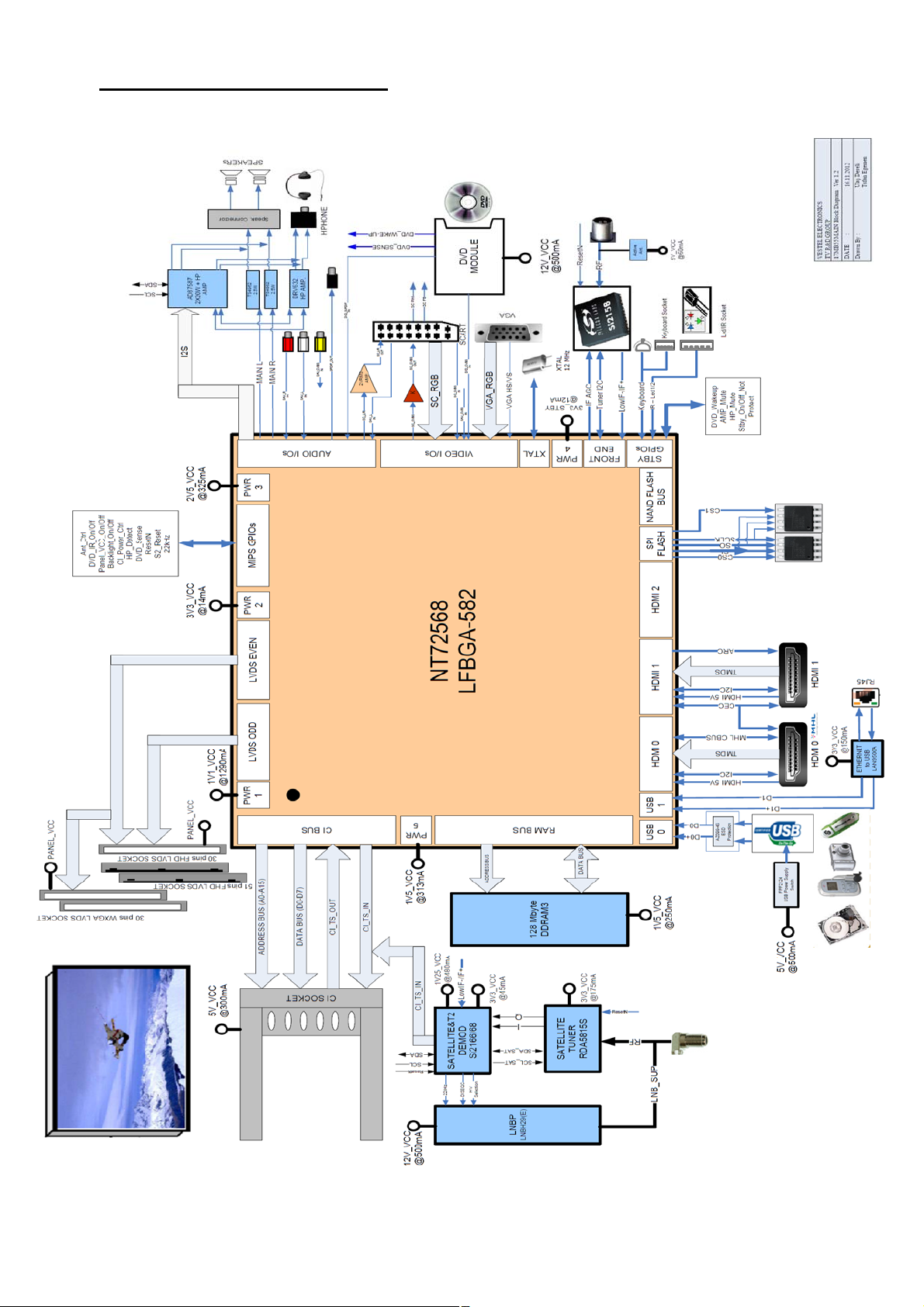
A. GENERAL BLOCK DIAGRAM
4
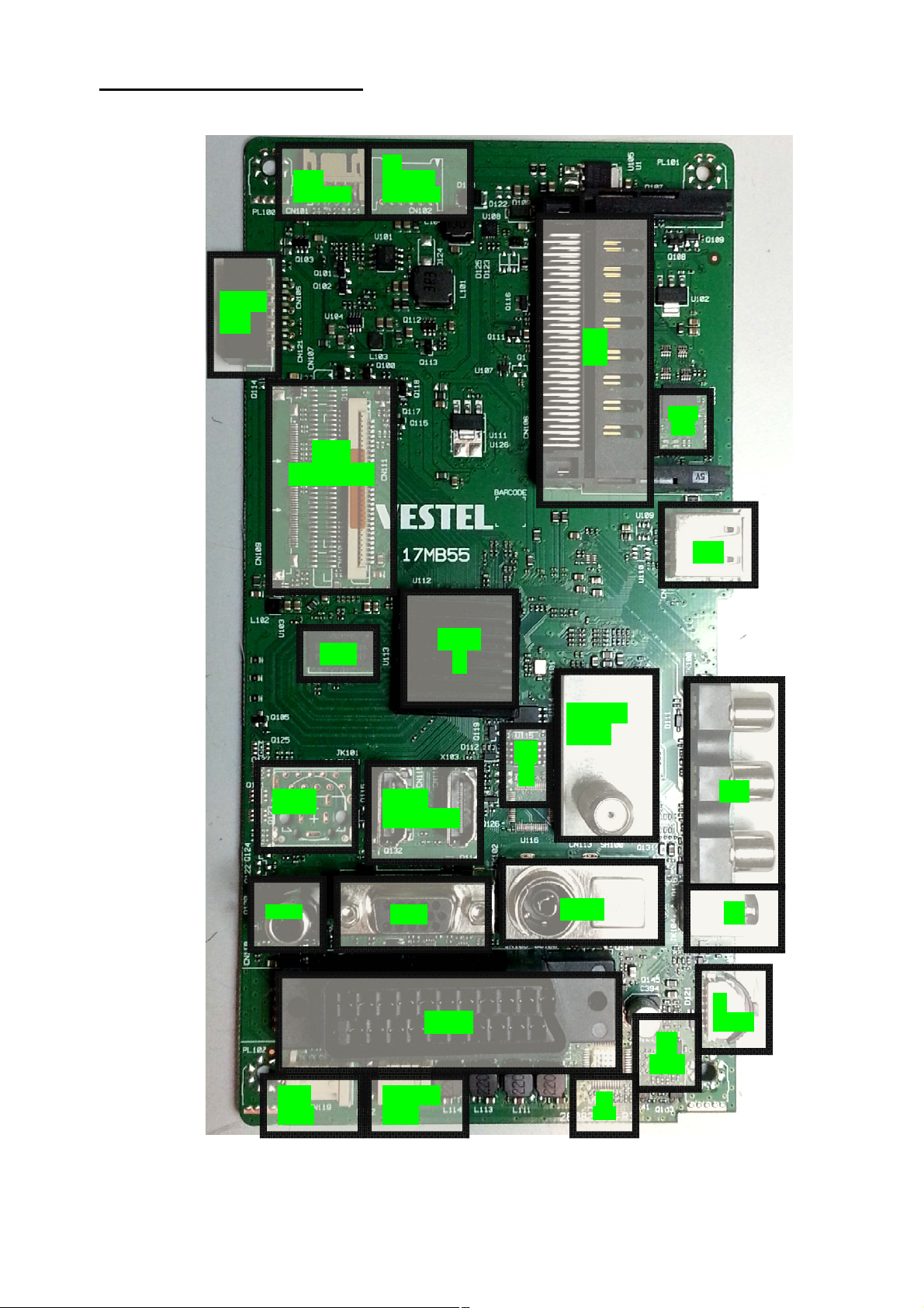
B. PLACEMENT OF BLOCKS
p
Power
Con.
DVD
Connector
LVDS
Connectors
Ext
converter
Connector
CI
T2/S2
Dem
USB
RJ45
S/PDIF
RAM
VGA
MAIN
IC
HDMI
Connectors
SCART
Satellite
Tuner
SPI
FL
SAV
Tuner
HP
3WAY
HP
Amp
LED
CON
SPEAK.
CON
6W
Am
5

2. T/T2/C/A TUNER (U119)
The Si2158 is Silicon Labs' fourth-generation hybrid TV tuner supporting all worldwide terrestrial and
cable TV standards. Requiring no external balun, SAW filters, wire wound inductors or LNAs, the Si2158
offers the lowest-cost BOM for a hybrid TV tuner. Also included are an integrated power-on reset circuit and
an option for single power supply operation. As with prior-generation Silicon Labs TV tuners, the Si2158
maintains very high linearity and low noise to deliver superior picture quality and a higher number of received
stations when compared to other silicon tuners and discrete MOPLL-based tuners. The Si2158 also incorporates
a harmonic-rejection mixer to deliver excellent Wi-Fi and LTE immunity. For the best performance with next-
generation digital TV standards such as DVB-T2/C2, the Si2158 delivers industry-leading phase noise
performance.
Features
Worldwide hybrid TV tuner
o Analog TV: NTSC, PAL/SECAM
o Digital TV: ATSC/QAM, DVBT2/T/C2/C, ISDB-T/C, DTMB
o 42-1002 MHz frequency range
Industry-leading margin to A/74,NorDig, DTG, ARIB, EN55020,OpenCable™
Lowest BOM for a hybrid TV tuner
o No balun at RF input
o Integrated tracking filters requiring no external inductors or SAW filters
o Increased ESD protection on 6 pins
Best-in-class real-world reception
o Exceeds MOPLL-based tuners
o Lowest phase noise
o High Wi-Fi and LTE immunity
Low power consumption
o 3.3 V and 1.8 V power supplies
o 3.3 V single-supply option
Integrated power-on reset circuit
Single or separate output pins for ALIF/DLIF connection to SoC
Standard CMOS process
4 x 4 mm, 28-pin QFN package
RoHS compliant
6
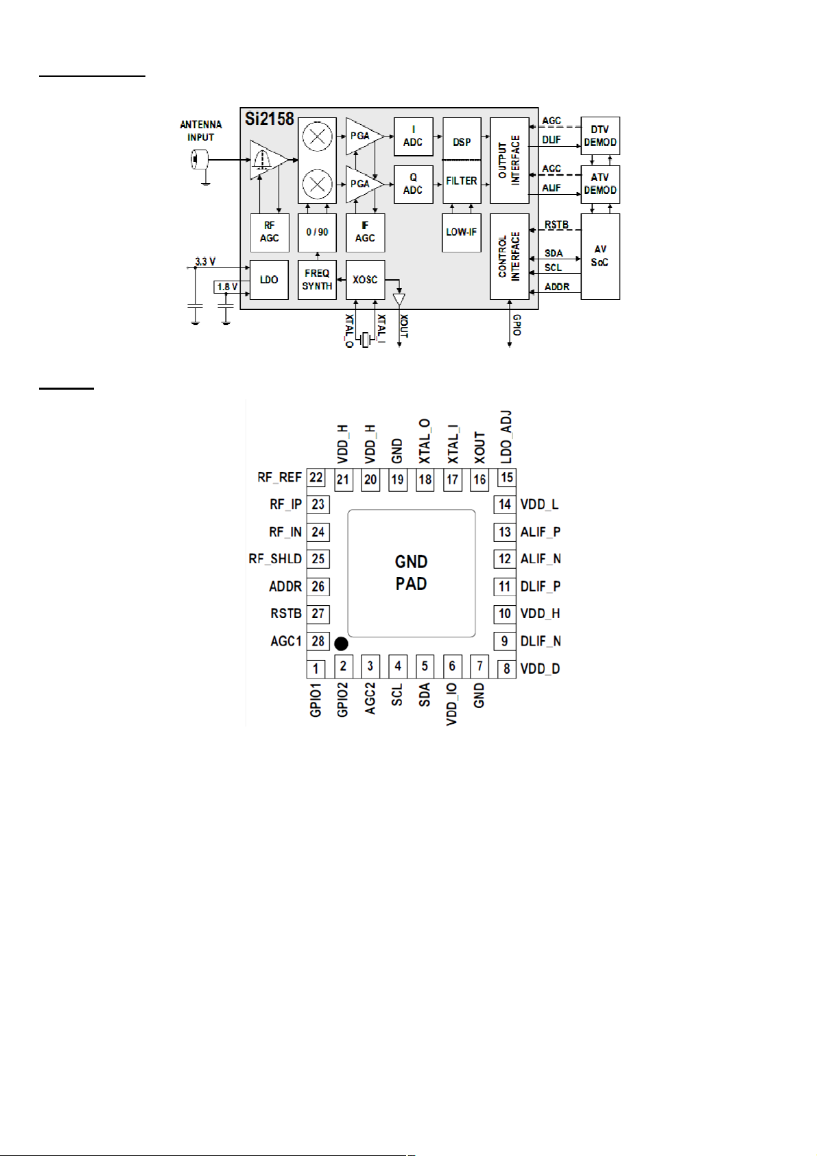
Block Diagram
Pinning
7

3. S/S2 TUNER (U125) OPTIONAL
The RDA5815s is a fully integrated direct conversion RF front end for DVB-S,DVB-S2&ABS-S,MMDS
digital satellite Reception standard CMOS process. The receiving frequency range is from 250MHz to
2150MHz, and the baseband filter’s bandwidth can be selected from 4MHz to 40MHz with 1MHz step.
The RDA5815s consists of a variable gain LNA, quadrature down converter, variable IF gain amplifiers,
variable low-pass filters, reference oscillator, VCOs, synthesizer and output baseband amplifier to drive
external ADC.
Based on RDA’s some innovative technique, the rda5815s offers excellent phase noise and very low
implementation loss, required for advanced modulation systems such as 8PSK and DVB-S2. This tuner RF IC
does not require a balun and its fully integrated design saves valuable board space and simplifies RF layout.
Features
Single-Chip RF to baseband Satellite receiver
CMOS Fully integrated RF front end
Low noise and wide dynamic range zero IF receiver
Input frequency range:250 to 2150 MHz
Input signal level: -100 to 5dBm
More than 85dB gain control range
Fully integrated PLL
Integrated RX VCO
Integrated baseband LPF with selectable cut-off frequency from 4Mhz to 40Mhz with 1Mhz step
Integrated LNA with RF AGC
Integrated reference oscillator
I2C bus interface
Automatic gain control
0.11um RF CMOS technology
3V to 3.6V operations
Power consumption of less than 600mW
Lower profile packages 4X4mm QFN24
8

Block Diagram
Pinning
9
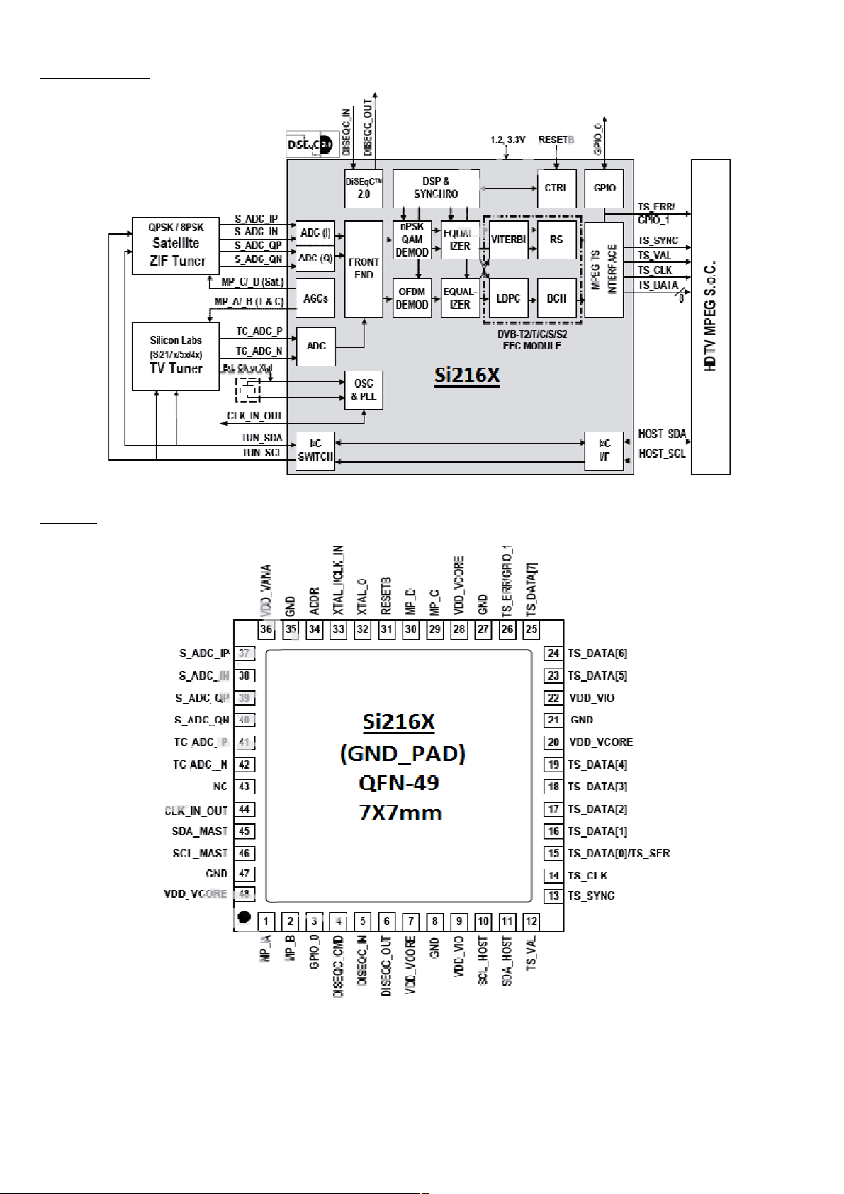
4. T2 or S/S2 DEMODULATOR (U106) OPTIONAL
The Si216X family has 3 different IC which are pin to pin compatible. DVB-S/S2 is supported by Si2166
and DVB-T2 is supported by Si2168.
10
Features
11
Block Diagram
Pinning
12

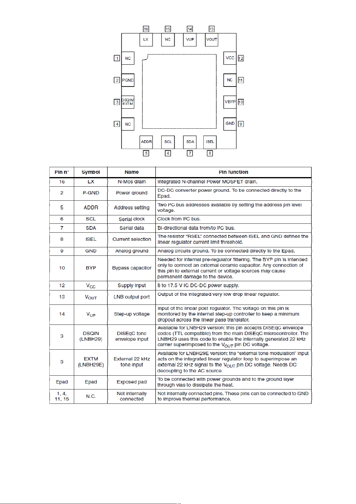
5. LNB SUPPLY and CONTROL IC (U108) WITH SAT OPTIONAL
Intended for analog and digital satellite receivers/Sat-TV and Sat-PC cards, the LNBH29 series is a
monolithic voltage regulator and interface IC, assembled in QFN16 (3x3) and QFN16 (4x4) specifically
designed to provide the 13 / 18 V power supply and the 22 kHz tone signaling to the LNB down-converter in
the antenna dish or to the multi-switch box. In this application field, it offers a complete solution with
extremely low component count, low power dissipation together with a simple design and I²C standard
interfacing.
This IC has a built-in DC-DC step-up converter that, from a single source from 9 V to 17.5 V, generates the
voltages (VUP) that allow the linear post-regulator to work with a minimum.
Dissipated power of 0.5 W typ. @ 500 mA load (the linear post-regulator drop voltage is internally kept at
VUP - VOUT = 1 V typ.). The IC is also provided with an under voltage lockout circuit that disables the whole
circuit when the supplied VCC drops below a fixed threshold (4.7 V typically). The step-up converter is
provided with a soft-start function which reduces the inrush current during startup. The SS time is internally
fixed at 4 ms typ. To switch from 0 to 13 V and 6 ms typ. to switch from 0 to 18 V.
Features
Complete interface between LNB and I²C bus
Built-in DC-DC converter for single 12 V supply operation and high efficiency (typ. 93% @ 0.5 A)
Selectable output current limit by external resistor
Compliant with main satellite receiver output voltage specifications
Accurate built-in 22 kHz tone generator suits widely accepted standards
EXTM pin, auxiliary 22 kHz modulation input (LNBH29E) extends design flexibility
22 kHz tone waveform integrity guaranteed also at no load condition
Low-drop post regulator and high efficiency step-up PWM with integrated power N-MOS allowing low
power losses
Overload and over temperature internal protection with I²C diagnostic bits
LNB short-circuit dynamic protection
+/- 4 kV ESD tolerant on output power pins
13

Block Diagram
Pinning
14
15

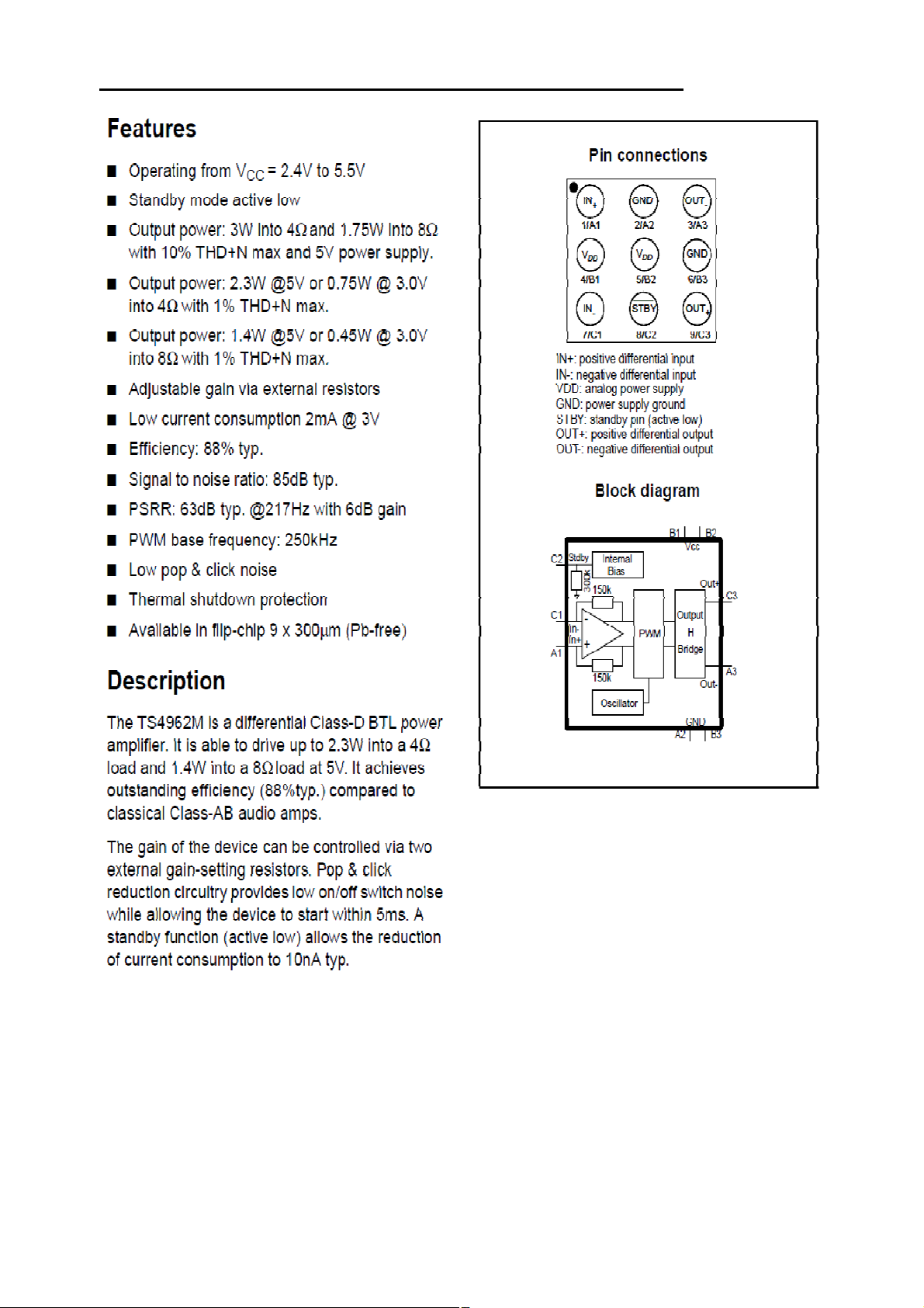
6. AUDIO AMPLIFIER ST AGE
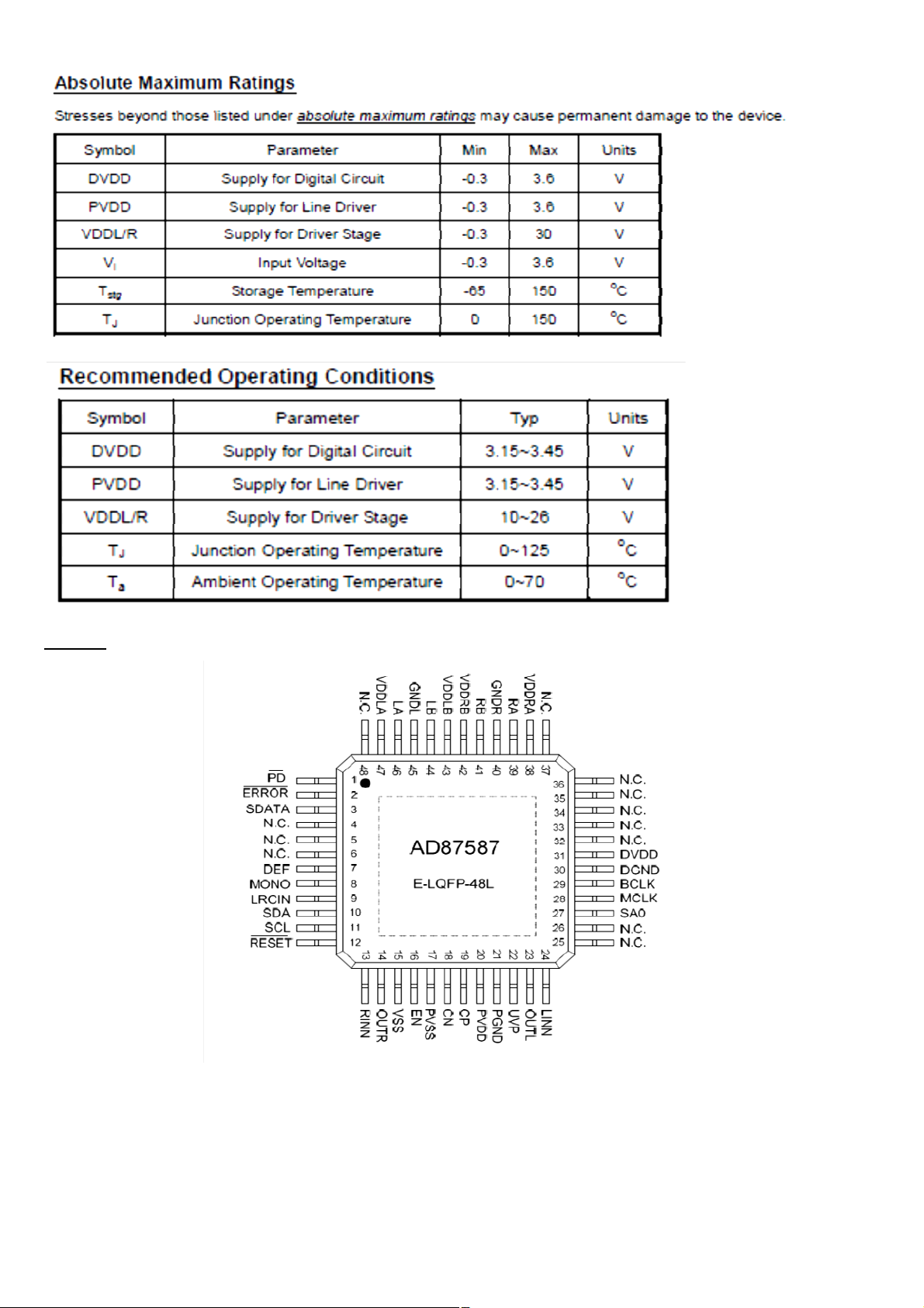
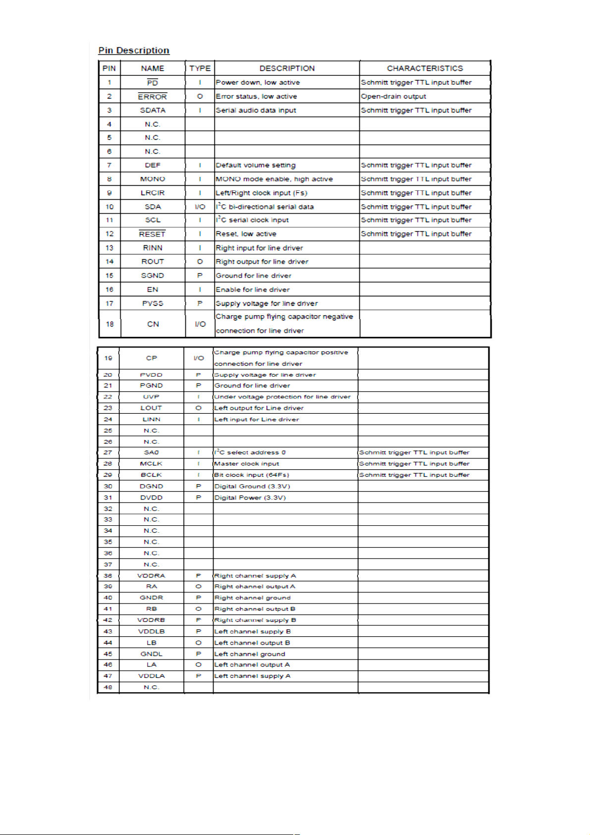
AD87587 (U124) (OPTIONAL FOR 6W and 8W PRODUCTS)
A.
The AD87587 is an integrated audio system solution, embedding digital audio process, power stage
amplifier, and a stereo 2Vrms line driver, for driving stereo bridge-tied speakers and headphone. Using I2C
digital control interface, the user can control AD87587’s input format selection, mute and volume control
functions. AD87587 has many built-in protection circuits to safeguard AD87587 from connection errors. It can
provide 20W output power to stereo amplifiers or 40W output power for mono applications.
Features
16/18/20/24-bit input with I2S, Left-alignment and Right-alignment data format
PSNR & DR(A-weighting) Loudspeaker: 97dB (PSNR), 105dB (DR) @ 24V
Multiple sampling frequencies (Fs)
32 kHz/ 44.1 kHz / 48 kHz and
64 kHz/ 88.2 kHz / 96 kHz and
128 kHz/176.4 kHz/192 kHz
System clock = 64x, 128x, 256x, 384x, 512x, 768x,1024x Fs
256x~1024x Fs for 32 kHz/ 44.1 kHz / 48 kHz
128x~512x Fs for 64 kHz/ 88.2 kHz / 96 kHz
64x~256x Fs for 128 kHz/176.4 kHz/192 kHz
Supply voltage
3.3V for digital circuit
10V~26V for loudspeaker driver
Loudspeaker output power for Stereo@ 24V
10W x 2ch into 8_ @ 0.16% THD+N
15W x 2ch into 8_ @ 0.18% THD+N
20W x 2ch into 8_ @ 0.24% THD+N
Sounds processing including:
Volume control (+24dB~-103dB, 0.125dB/step)
Dynamic range control
Power clipping
Channel mixing
User programmed noise gate
DC-blocking high-pass filter 1
Anti-pop design
Short circuit and over-temperature protection
16
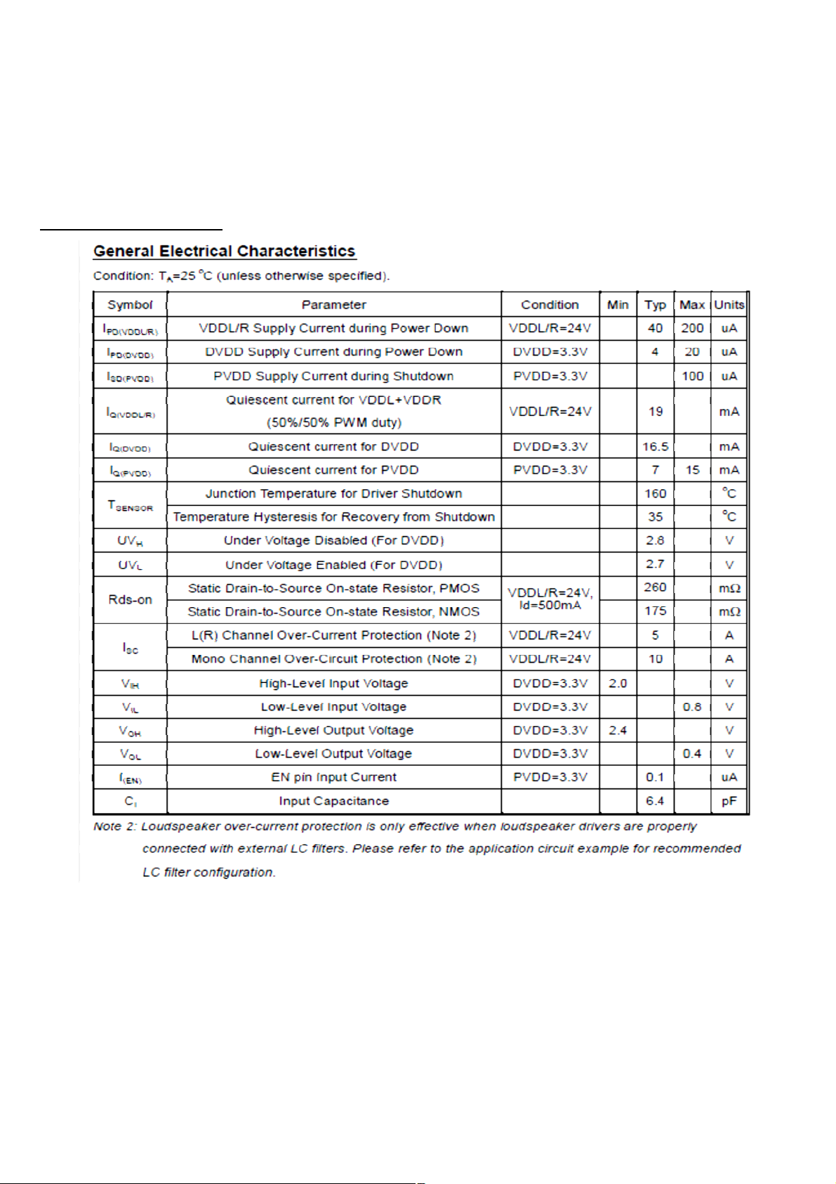
I2C control interface with selectable device address
Internal PLL
LV Under-voltage shutdown and HV Under-voltage detection
Power saving mode
Dynamic temperature control
Electrical Characteristics
17
18
Pinning
19
20
B. TS4962M (U122 & U123) (OPTIONAL FOR 2.5W PRODUCTS)
21
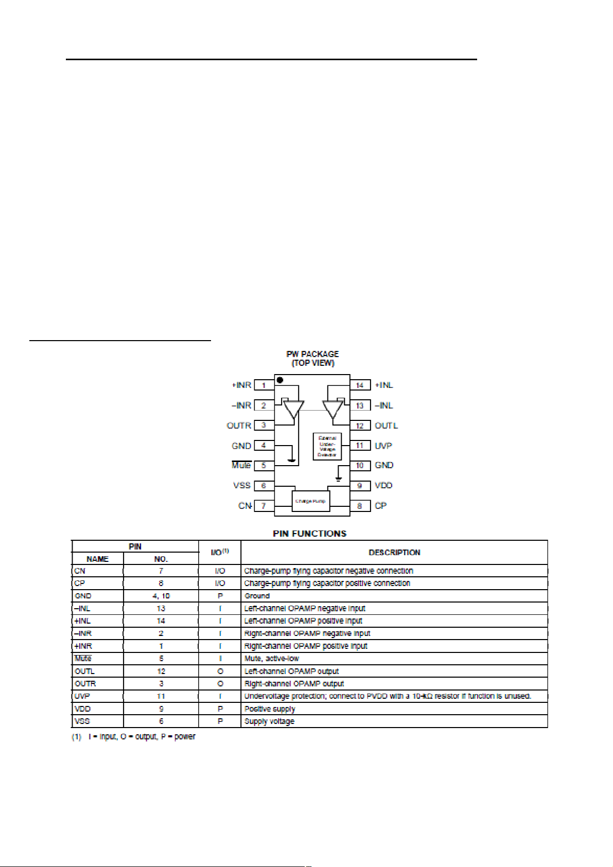
C. DRV632 (U121) (OPTIONAL HP DRIVER FOR 2.5W PRODUCTS)
The DRV632 is a 2-VRMS pop-free stereo line driver designed to allow the removal of the output dc-
blocking capacitors for reduced component count and cost. The device is ideal for single-supply electronics
where size and cost are critical design parameters.
The DRV632 is capable of driving 2 VRMS into a 10-k load with 3.3-V supply voltage. The device has
differential inputs and uses external gain-setting resistors to support a gain range of ±1 V/V to ±10 V/V, and
gain can be configured individually for each channel. The DRV632 has built-in active-mute control for pop-free
audio on/off control. The DRV632 has an external under voltage detector that mutes the output when the power
supply is removed, ensuring a pop-free shutdown.
The DRV632 does not require a power supply greater than 3.3 V to generate its 5.6-Vpp output, nor does it
require a split-rail power supply. The DRV632 integrates its own charge pump to generate a negative supply
rail that provides a clean, pop-free ground-biased 2-VRMS output. The DRV632 is available in a 14-pin
TSSOP.
Pin Description and Package View
22
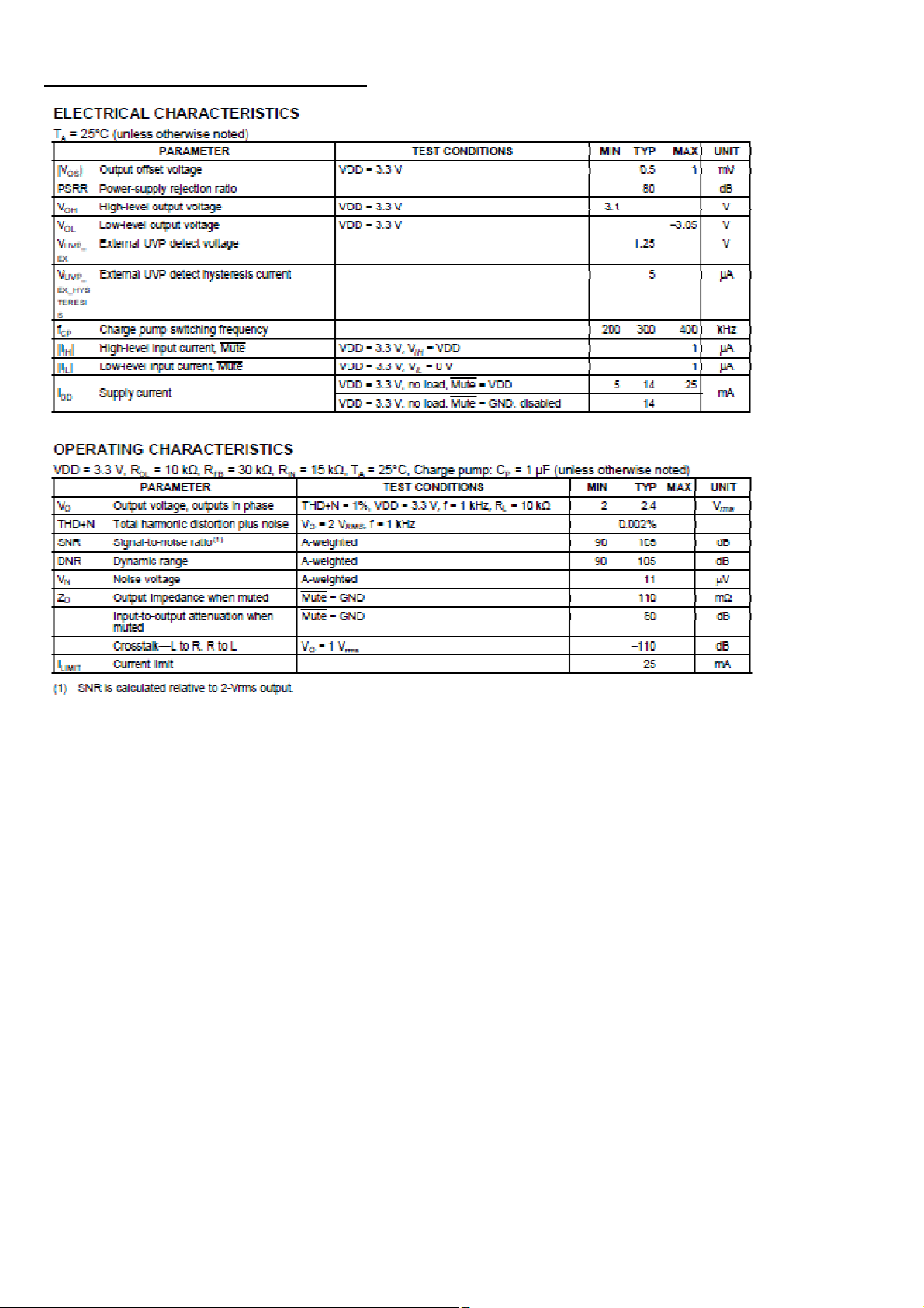
Electrical and Operating Characteristics
7. POWER STAGE
The DC voltages required for different blocks of the main board and panel are provided by main power
supply unit. MB55 chassis can operate with PW05, IPS60, IPS61, IPS70, IPS20, IPS11, IPS16, IPS17, IPS19,
PW25, PW26, PW03, PW04, PW06, and PW07 as main power supply and also with 12V adaptor. The main
difference from previous projects MB55 uses the 2x6 pin power connector. And only 12V_STBY supply is
necessary to provide all required board supplies. As the main power board has 2x6 pin option, MB55 can
operate with above given power boards.
Which power board can be used for board to board or cable connection?
Board to board (BTB): PW05, IPS60, IPS61, IPS70, IPS11, IPS16, IPS17, IPS19
Power Cable: PW25, PW26, PW03, PW04, PW06, PW07, IPS20,
The power supplies generate 12V standby mode DC voltage and 24V system voltage only for audio IC
voltage in necessary situations. Power stage which is on-chassis generates 5V, 3V3 stand by voltage and 12V,
5V, 3V3, 2.5V, 1.5V, 1.2 and 1.15V supplies for other blocks of the chassis. The power block diagram with the
23
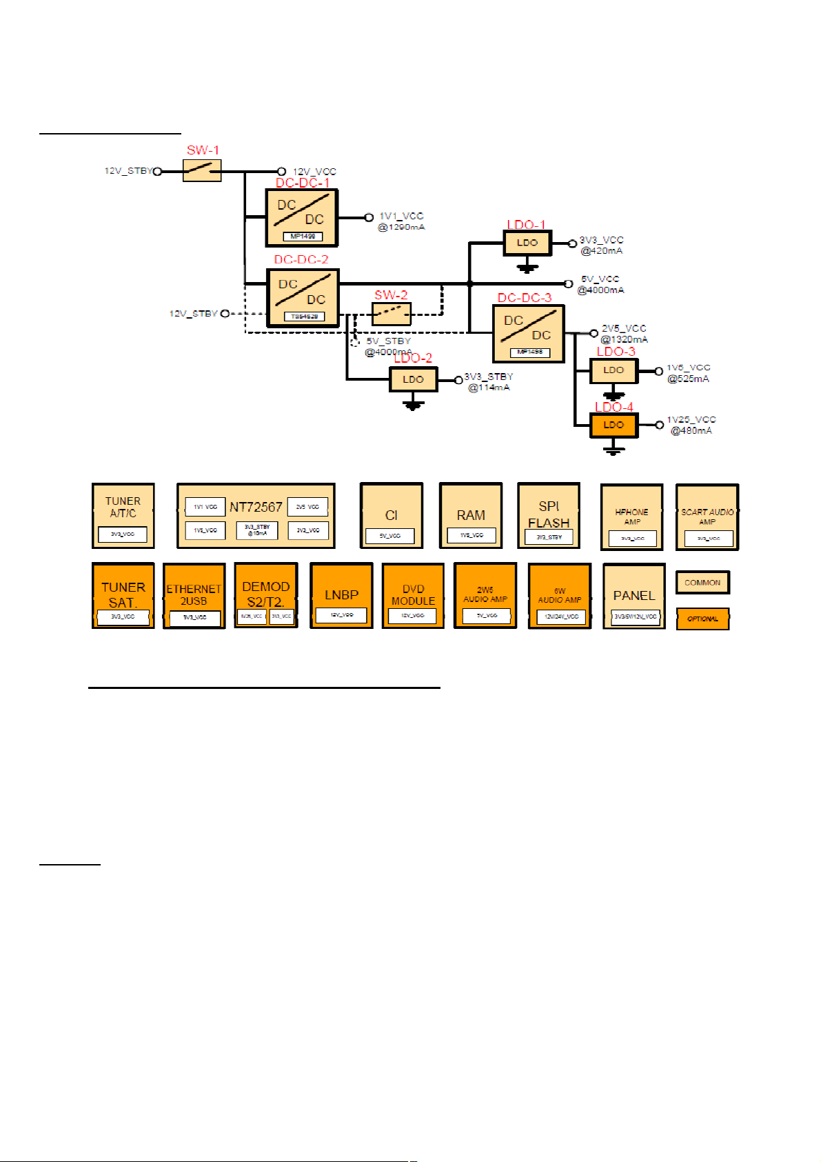
blocks power requirements of MB55 is given below. And also you can find below the details about the Step
down IC’s and LDO’s which are used in MB55 main board.
Power Management
A. RT7278 (U101) (3A) – RT7240 (U101) (5A)
The RT7278/RT7240 is a synchronous step down converter with Advanced Constant On-Time (ACOT)
mode control. The ACOT provides a very fast transient response with few external components. The low
impedance internal MOSFET supports high efficiency operation with wide input voltage range from 4.5V to
17V. The proprietary circuit of the RT7278/RT7240 enables to support all ceramic capacitors. The output
voltage can be adjustable between 0.8V and 8V. The soft-start is adjustable by an external capacitor.
Features
ACOT Mode Enables Fast Transient Response
4.5V to 17V Input Voltage Range
3A Output Current
60mOhm Internal Low Site N-MOSFET
Advanced Constant On-Time Control
Support All Ceramic Capacitors
Up to 95% Efficiency
24
 Loading...