


1. INTRODUCTION
Analog front end consist of a main tuner, a pip tuner and IF decoders. The PLL tuners
supply the IF signals and SAW filters are used for filtering and impedance matching between
demodulator ICs and tuners. The main IF signal is demodulated by demodulator (DRX3961A)
and the pip IF signal is demodulated by (TDA9885T). At the outputs of the demodulators, CVBS
and QSS signals are obtained.
The main tuner CVBS, pip tuner CVBS, FAV CVBS, Scart1 CVBS, SVHS_Y, Scart2
CVBS/Y, DMP CVBS, IDTV/Scart3 CVBS/Y signals are applied to the video matrix switch
(TEA6415). The outputs of the switch are main CVBS to video processor; pip CVBS to video
decoder, scart1_out CVBS to scart1, scart2_out CVBS to scart2, scart3_out CVBS to scart3.
The video decoder IC (VPC3230) decodes to CVBS signal for the pip picture. The source
for the pip picture can be CVBS from the video matrix switch, SVHS, Scart1, Scart2, Scart3 and
DMP. The output of the decoder is 8 bits ITU601_PIP signal connected to video processor IC
SVP LX66.
SVP-LX66 can support up to 1920x1080p panel. It consists of OSD, teletext, scaler,
deinterlacer, 8/10-bit dual LVDS transmitter and HDMI blocks. The inputs to SVP LX66 are
Scart2 RGB/DMP RGB, SC2/SC3 Chroma/SVHS Chroma, Scart1 RGB, main CVBS from video
matrix switch, YPbPr, ITU601_PIP, HDMI, ITU601_IDTV, PC RGB. The output is the 8bits
LVDS signal to the panel.The SVP LX66 uses a DDR RAM (EM6A9320) for faster processing.
The main controller IC is M16C-M30620SPGP. The I/O assignments are as follows:
NAME TYPE DESCRIPTION Port Pin
HDMI RELATED
1 HDMI_HPLG OUT HotPlug output for HDMI-1 source
P1.4 76
device
2 HDMI_HPLG2 OUT HotPlug output for HDMI-2 source
P8.0 22
device
3 HDMI_CEC IN (*) CEC input from HDMI cable P1.5 75
4 HDMI_DTC IN HDMI detection for first input P8.6 11
5 HDMI_DTC2 IN HDMI detection for second input P8.7 10
6 HDMI_DDC_WP OUT HDMI NVM write protect control for
P9.4 3
service
7 SCDT IN (*) Sync Change Detection for HDMI P8.4 18
POWER / PANEL RELATED
8 PROTECT IN Indicates the power supply status P1.7 73
9 STBY / CPU_GO OUT Controls the power supply on or off P1.3 77
10 BLIGHT /
OUT Controls the backlight P1.2 78
PDP_GO
11 DISP_EN OUT Controls the display enable or disable P1.1 79
12 BLIGHT_LVL PWM OUT Controls the backlight level P7.6 24
13 PANEL_VCC OUT Controls the power supply of the panel P1.0 80
SERIAL DATA COMMUNICATION
14 SDA IN/OUT I2C serial data line P7.2 28
15 SCL OUT I2C clock line P7.3 27
16 E2_SDA IN/OUT I2C serial data line for E2PROM P10.7 89
17 E2_SCL OUT I2C clock line for E2PROM P10.6 90
18 E2_WP OUT Controls the write protection of the
P10.5 91
E2PROM
EXTENTION MODULES RELATED
19 IDTV_RX IN IDTV UART receive P6.2 36
20 IDTV_TX OUT IDTV UART transmit P6.3 35
21 IDTV_IRQ OUT IDTV status change notification P6.1 37
22 TVLINK IN (*) /
TVLink interrupt input / data output P1.6 74
OUT
23 DMP_CTRL OUT Controls DMP module P6.0 38
VIDEO RELATED
24 LX_RST OUT Resets the LX66 video processor P8.1 21
25 LX_INT IN (*) Interrupt notification from LX66 P8.3 19
26 RGB_SW_1 OUT RGB switch control 1 P9.2 5
27 RGB_SW_2 OUT RGB switch control 2 P9.3 4
APPLICATION
28 IR IN (*) Remote control interrupt input P8.2 20
29 LED_1 OUT LED control 1 P9.0 7
30 LED_2 OUT LED control 2 P9.1 6
31 MUTE_AMP OUT Mutes the audio amplifier P9.7 100
32 SC1_PIN8 ADC IN Scart 1 pin8 input measurement P10.1 95
33 SC2_PIN8 ADC IN Scart 2 pin8 input measurement P10.2 94
34 SC3_PIN8 ADC IN Scart 3 pin8 input measurement P10.3 93
35 KEYB ADC IN Keyboard input P10.0 97
36 SWU_RX IN UART receive for software upgrade P7.1 29
37 SWU_TX OUT UART transmit for software upgrade P7.0 30
38 RY_BY IN Ready/Busy indication from external
P5.1 45
flash
39 LG_1/IRQPDP IN Interrupt Request from Plasma Display P7.4 26
41 CHROMA_SW OUT Chroma Switch for SVHS P7.5 25
42 DRX_RST OUT DRX reset P9.6 1
43 VGA_STBY IN PC VGA standby detection P9.5 2
44 SERV_DTC IN Service socket detection P7.7 23
45 AC_INFO IN Alternate Current Information P8.5 18
Table 1: Microcontroller I/O Assignments
The PC Audio L/R, DMP Audio L/R, IDTV/SC3 Audio L/R, YPbPr Audio L/R, Scart2
Audio L/R signals are switched via audio switch TEA6420. The outputs of the switch are two
L/R audio signals.
MSP4411K is used for audio processing and it covers the sound processing of all analog
TV-standards worldwide, as well as the NICAM digital sound standard. Audio outputs are
connected to SC1/2/3 connector, audio line out, headphone, Speaker, subwoofer and S/PDIF
connectors. The inputs to the MSP441K are two audio signals from audio switch,
FAV_Audio_L/R, SC1_Audio_L/R, QSS signals from main and pip tuners, Tuner2 mono signal
and HDMI I2S signal.
The AD8190 is a DVI/HDMI switch featuring equalized TMDS inputs and preemphasized TMDS outputs, ideal for systems with long cable runs between sources and sinks of
video data. A disable feature sets the outputs to a high impedance state, reducing the power
dissipation.
The primary function of the AD8190 is to switch one of two HDMI single-link sources to
one output. Each HDMI source consists of four differential high-speed channels and four general
purpose control lines. The switched HDMI signal is sent to the video processor IC.

2. CONTROLLER
2.1. Microcontroller: Renesas M16C M30620SPGP
General Description:
The M16C/62P Group (M16C/62P, M16C/62PT) of single-chip microcomputers are built
using the high performance silicon gate CMOS process using a M16C/60 Series CPU core and
are packaged in a 80-pin, 100-pin and 128-pin plastic molded QFP. These single-chip
microcomputers operate using sophisticated instructions featuring a high level of instruction
efficiency. With 1M bytes of address space, they are capable of executing instructions at high
speed. In addition, this microcomputer contains a multiplier and DMAC which combined with
fast instruction processing capability, makes it suitable for control of various OA, communication,
and industrial equipment which requires highspeed arithmetic/logic operations.
General Features:
Main features of M16C are:
• 16-bit Multifunction Timer (Timer A and B): 11 channels
• UART/Clock Synchronous Serial Interface: 3 channels
• Clock Synchronous Serial Interface: 2 channels
• 10-bit A/D Converter: 26 channels
• 8-bit D/A Converter: 2 channels
• DMAC: 2 channels
• CRC Calculation Circuit
• Watchdog Timer
• Clock Generation Circuits: Main Clock Generation Circuit, Sub Clock Generation
Circuit, On-chip Oscillator, PLL Synthesizer
• Oscillation Stop Detection Function
• Voltage Detection Circuit (Option) (Except for T Version and V Version)
• Interrupts: 29 internal factors, 8 external factors, 4 software factors
• Data Flash: 4KB (Flash Memory Version only)
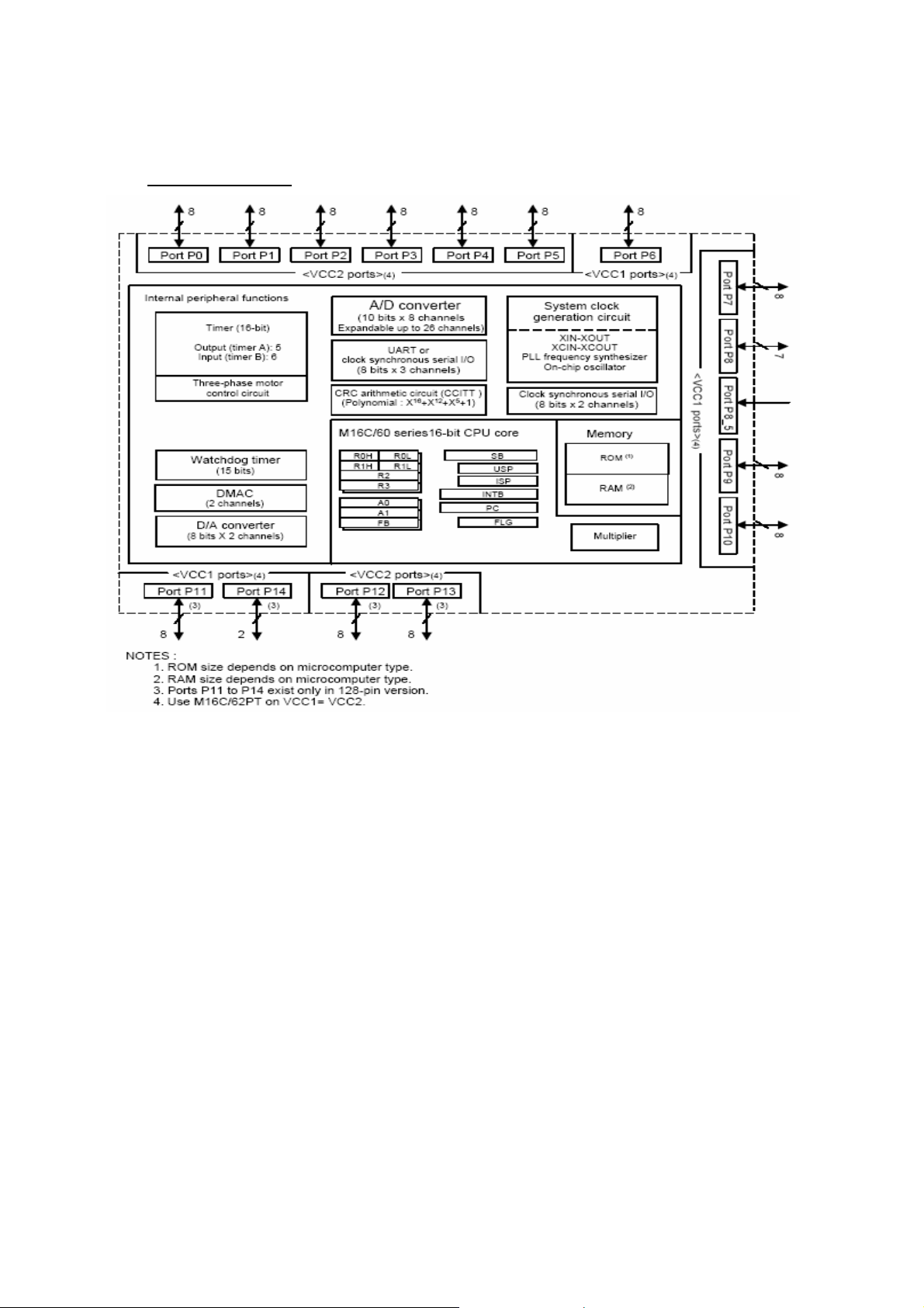
Block Diagram:
Figure 1: M16C Block Diagram
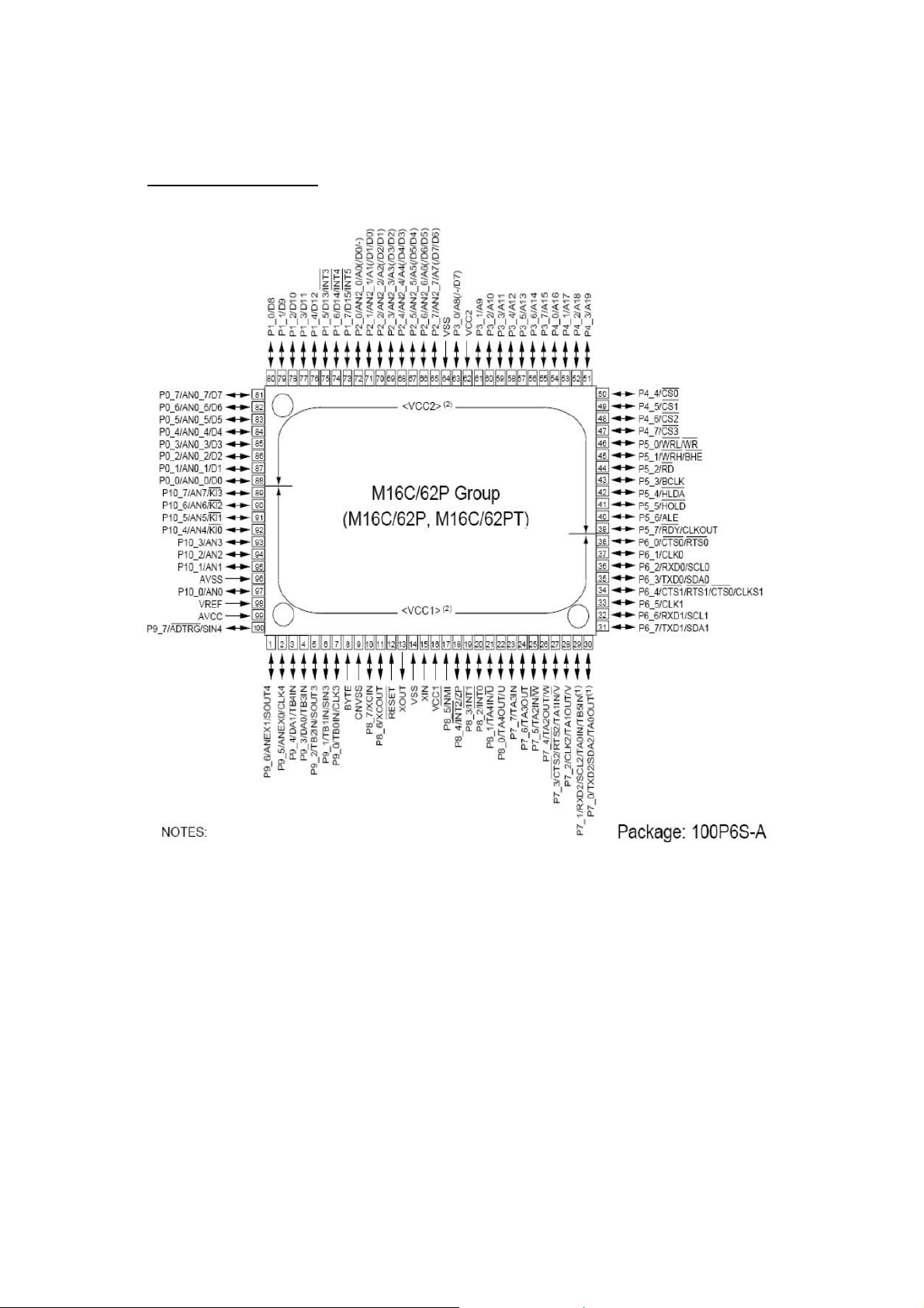
Pin Configuration:
Figure 2: M16C Pin Configuration


Table 2: M16C Pin Descriptions

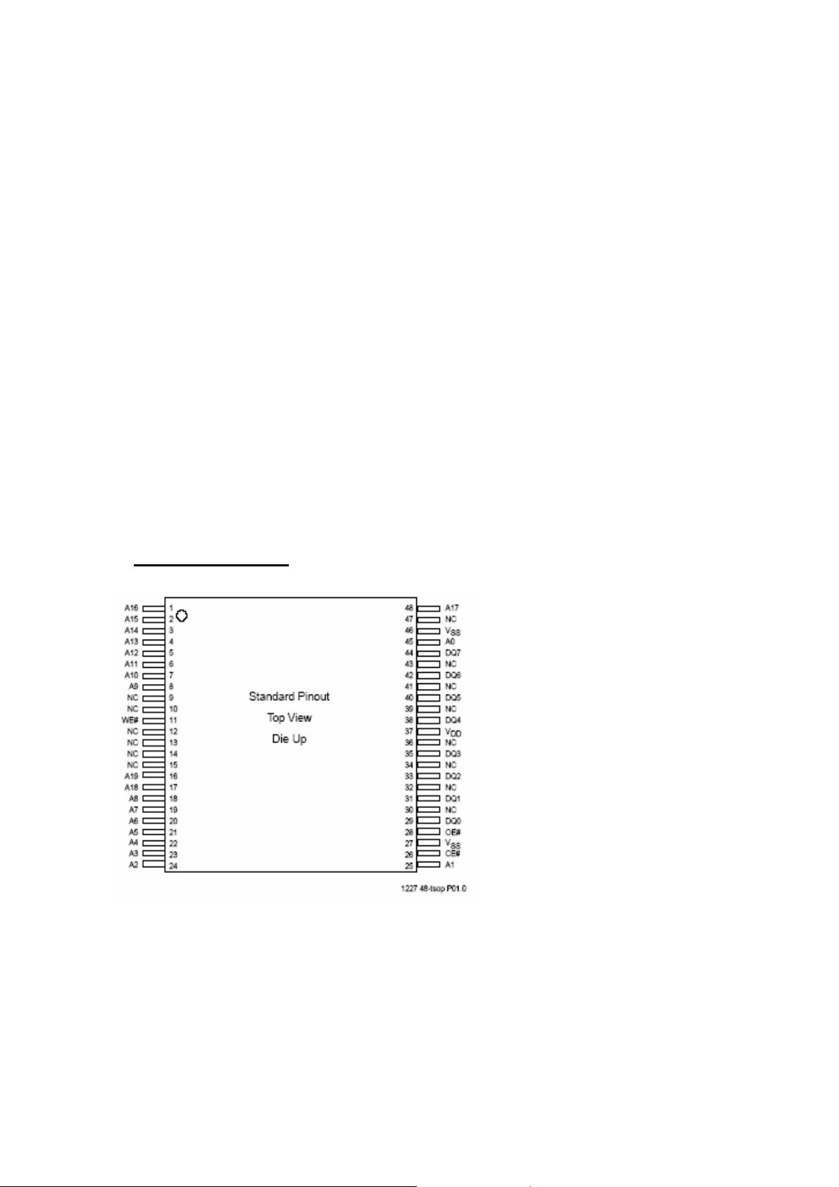
2.2. Flash IC SST39VF088
General Description:
The SST39VF088 device is a 1M x8 CMOS Multi-Purpose Flash (MPF) manufactured with
SST’s proprietary, high performance CMOS SuperFlash technology. The split-gate cell design
and thick-oxide tunneling injector attain better reliability and manufacturability compared with
alternate approaches. The SST39VF088 writes (Program or Erase) with a 2.7-3.6V power supply.
It conforms to JEDEC standard
pinouts for x8 memories. Featuring high performance Byte-Program, the SST39VF088 device
provides a typical Byte-Program time of 14 µsec. The devices use Toggle Bit or Data# Polling to
indicate the completion of Program operation. To protect against inadvertent write, they have onchip hardware and
Software Data Protection schemes. Designed, manufactured, and tested for a wide spectrum of
applications, these devices are offered with a guaranteed endurance of 10,000 cycles. Data
retention is rated at greater than 100 years.The SST39VF088 device is suited for applications that
require convenient and economical updating of program, configuration, or data memory. For all
system applications, they significantly improve performance and reliability, while lowering
power consumption. They inherently use less energy during Erase and Program than alternative
flash technologies. The total energy consumed is a function of the applied voltage, current, and
time of application. Since for any given voltage range, the SuperFlash technology uses less
current to program and has a shorter erase time, the total energy consumed during any Erase or
Program operation is less than alternative flash technologies. They also improve flexibility while
lowering the cost for program, data, and configuration storage applications.
The SuperFlash technology provides fixed Erase and Program times, independent of the number
of Erase/Program cycles that have occurred. Therefore the system software or hardware does not
have to be modified or de-rated as is necessary with alternative flash technologies, whose Erase
and Program times increase with accumulated Erase/Program cycles. To meet high density,
surface mount requirements, the SST39VF088 is offered in 48-lead TSOP packaging. See below
figure for pin assignments.
General Features:
• Organized as 1M x8
• Single Voltage Read and Write Operations
– 2.7-3.6V
• Superior Reliability
– Endurance: 100,000 Cycles (typical)
– Greater than 100 years Data Retention
• Low Power Consumption (typical values at 5 MHz)
– Active Current: 12 mA (typical)
– Standby Current: 4 µA (typical)
• Sector-Erase Capability
– Uniform 4 KByte sectors
• Block-Erase Capability
– Uniform 64 KByte blocks
• Fast Read Access Time:
– 70 and 90 ns
• Latched Address and Data
• Fast Erase and Byte-Program
– Sector-Erase Time: 18 ms (typical)
– Block-Erase Time: 18 ms (typical)
– Chip-Erase Time: 70 ms (typical)
– Byte-Program Time: 14 µs (typical)
– Chip Rewrite Time: 15 seconds (typical)
• Automatic Write Timing
– Internal VPP Generation
• End-of-Write Detection
– Toggle Bit
– Data# Polling
• CMOS I/O Compatibility
• JEDEC Standard
– Flash EEPROM Pinouts and command sets
• Packages Available
– 48-lead TSOP (12mm x 20mm)
Pin Configuration:
Figure 3: Flash IC Pin Configuration

Table 3:Flash IC Pin Descriptions
2.3. 32K I2C Serial EEPROM: 24LC32A
General Description:
The Microchip Technology Inc. 24AA32A/24LC32A (24XX32A*) is a 32 Kbit Electrically
Erasable PROM.The device is organized as four blocks of 8K x 8-bit memory with a 2-wire serial
interface. Low-voltage design permits operation down to 1.8V, with standby and active currents
of only 1 A and 1 mA, respectively. It has been developed for advanced, lowpower applications
such as personal communications or data acquisition. The 24XX32A also has a page write
capability for up to 32 bytes of data. Functional address lines allow up to eight devices on the
same bus, for up to 256 Kbits address space. The 24XX32A is available in the standard 8-pin
PDIP, surface mount SOIC,
TSSOP and MSOP packages.
General Features:
• Single supply with operation down to 1.8V
• Low-power CMOS technology
- 1 mA active current typical
- 1A standby current (max.) (I-temp)
• Organized as 4 blocks of 8K bits (32K bit)
• 2-wire serial interface bus, I2C™ compatible
• Cascadable for up to eight devices
• Schmitt Trigger inputs for noise suppression
• Output slope control to eliminate ground bounce
• 100 kHz (<2.5V) and 400 kHz (2.5V)
compatibility
• Self-timed write cycle (including auto-erase)
• Page write buffer for up to 32 bytes
• 2 ms typical write cycle time for page write

• Hardware write-protect for entire memory
• Can be operated as a serial ROM
• Factory programming (QTP) available
• ESD protection > 4,000V
• 1,000,000 erase/write cycles
• Data retention > 200 years
• 8-lead PDIP, SOIC, TSSOP and MSOP packages
• Standard and Pb-free finishes available
• Available temperature ranges:
- Industrial (I): -40°C to +85°C
- Automotive (E): -40°C to +125°C
Block Diagram:
Figure 4: Serial EEPROM Block Diagram
Pin Configuration:
Figure 5: Serial EEPROM Pin Configuration

3. TUNING AND IF DECODING
3.1. Tuner
The tuners used in the design are combined VHF, UHF tuners suitable for CCIR systems
B/G, H, L, L’, I/I’, and D/K. The tuning is available through the digitally controlled I2C bus
(PLL). Below you will find info on one of the tuners in use.
Description:
The UV1316MK4 tuner belongs to the UV1300 family of third generation WSP tuners,
which are designed to meet a wide range of TV applications. It is a full band tuner suitable for
CCIR systems B/G, H, L, L’, I and I’. The low IF output impedance is designed for direct drive
of a wide variety of SAW filters with sufficient suppression of triple.
Features:
Member of UV1300 MK4 family of small-sized UHF/VHF tuners
• Systems CCIR: B/G, H, L, L’, I and I’; OIRT: D/K
• Digitally-controlled (PLL) tuning via I2C-bus
• Fast 400kHz I2C bus protocol compatible with 3.3V and 5V micro controllers
• Off-air, S-cable and hyperband channels from 48.25 MHz to 863.25MHz inclusive
• World standardized mechanical dimensions and pinning. Horizontal mounting is
optionally available
• Various connector types available
• EURO content available.
Pin Configuration:
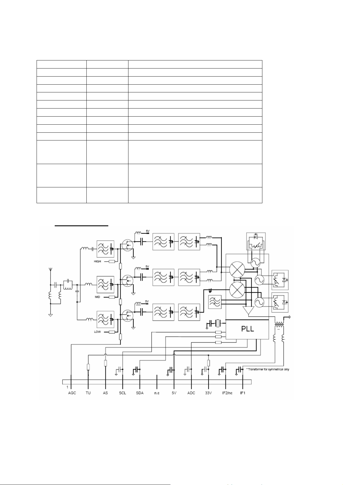
Pin Symbol Description
1 AGC Automatic Gain Control Voltage
2 TU Tuning Voltage Monitor(Output)
3 AS I2C Bus Address Select
4 SCL I2C Bus Serial Clock
5 SDA I2C Bus Serial Data
6 N.C. Not Connected
7 Vs Supply Voltage +5V
8 ADC ADC Input
9 Vst Fixed Tuning Supply Voltage +32V
10 I.F out 2 /
d.n.c
11 I.F out 1
Symmetrical I.F output 2 / Do not connect
for asymmetrical
Asymmetrical I.F Output / Symmetrical I.F
output 1
M1,M2,M3,M4 GND
Table 4: UV1316 MK4 Pin Descriptions
Mounting Tags (Ground)
Block Diagram:
Figure 6: UV1316 MK4 Block Diagram
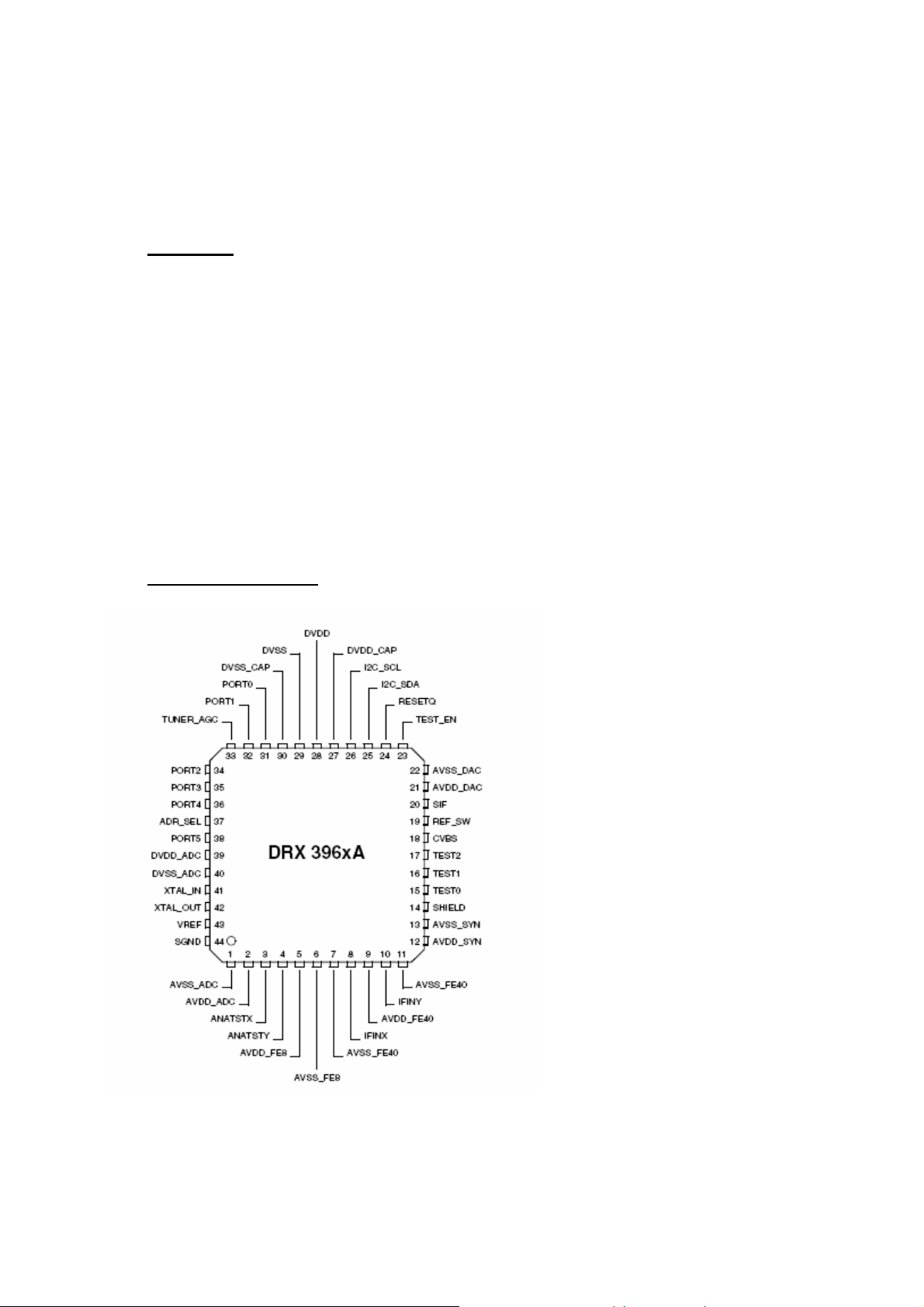
3.2. IF Demodulator: Micronas DRX3961A
DRX 3961A is used to extract CVBS and audio information from the IF output of the tuner.
Features:
• Multistandard QSS IF processing with a single SAW filter
• Programmable IF frequency between 30 and 60 MHz
• DSP-based IF processing for the following standards: B/G, D/K, I, L/L’, and M/N
• Standard specific digital signal processing for channel filtering, audio/video splitting,
group delay equalization (programmable), video AGC and delayed tuner AGC
• Digital picture carrier recovery
• Automatically frequency-adjusted Nyquist slope over complete lock-in frequency range,
which eliminates the need of fine tuning
• Fast AGC algorithms for tuner, video, and SIF outputs
• Programmable tuner take-over point (TOP)
• No sound traps required for video output
• FM radio capability without external components and with standard TV tuner
• I2C bus interface
Pin Configuration:
Figure 7: DRX 3961A Pin Configurations

Block Diagram:
Figure 8: DRX 3961A Block Diagram
3.3. IF Demodulator:TDA9886T
Description:
The TDA9886T is an alignment-free multistandard (PAL and NTSC) vision and sound IF
signal PLL demodulator for negative modulation only and FM processing.
The TDA9886 is an alignment-free multistandard (PAL, SECAM and NTSC) vision and sound
IF signal PLL demodulator for positive and negative modulation, including sound AM and FM
processing.
Features:
· 5 V supply voltage
· Gain controlled wide-band Vision Intermediate Frequency (VIF) amplifier, AC-coupled
· Multistandard true synchronous demodulation with active carrier regeneration: very linear
demodulation, good intermodulation figures, reduced harmonics, and excellent pulse response
· Gated phase detector for L and L-accent standard
· Fully integrated VIF Voltage Controlled Oscillator (VCO), alignment-free, frequencies
switchable for all negative and positive modulated standards via I2C-bus
· Digital acquisition help, VIF frequencies of 33.4, 33.9,38.0, 38.9, 45.75, and 58.75 MHz
· 4 MHz reference frequency input: signal from Phase-Locked Loop (PLL) tuning system or
operating as crystal oscillator
· VIF Automatic Gain Control (AGC) detector for gain control, operating as peak sync detector
for negative modulated signals and as a peak white detector for positive modulated signals
· External AGC setting via pin OP1
· Precise fully digital Automatic Frequency Control (AFC) detector with 4-bit digital-to-analog
converter, AFC bits readable via I2C-bus
· TakeOver Point (TOP) adjustable via I2C-bus or alternatively with potentiometer
· Fully integrated sound carrier trap for 4.5, 5.5, 6.0, and 6.5 MHz, controlled by FM-PLL
oscillator
· Sound IF (SIF) input for single reference Quasi Split Sound(QSS) mode, PLL controlled
· SIF-AGC for gain controlled SIF amplifier, single reference QSS mixer able to operate in high
performance single reference QSS mode and in intercarrier mode, switchable via I2C-bus
· AM demodulator without extra reference circuit
· Alignment-free selective FM-PLL demodulator with high linearity and low noise
· Four selectable I2C-bus addresses
· I2C-bus control for all functions
· I2C-bus transceiver with pin programmable Module Address(MAD)
Pin Configuration:
Symbol Pin Description
VIF1 1 VIF differential input 1
VIF2 2 VIF differential input 2
n.c. - not connected
OP1 3 output port 1; open-collector
FMPLL 4 FM-PLL for loop filter
DEEM 5 de-emphasis output for capacitor
AFD 6 AF decoupling input for capacitor
DGND 7 digital ground
n.c. - not connected
AUD 8 audio output
TOP 9
SDA 10
SCL 11 I2C-bus clock input
SIOMAD 12
n.c. - not connected
n.c. 13 not connected
n.c. - not connected
TAGC 14 tuner AGC output
REF 15
VAGC 16 VIF-AGC for capacitor
n.c. - not connected
CVBS 17 composite video output
n.c. - not connected
AGND 18 analog ground
VPLL 19 VIF-PLL for loop filter
tuner AGC TakeOver Point (TOP)
for resistor adjustment
I2C-bus data input and output
sound intercarrier output and MAD
select with resistor
4 MHz crystal or reference signal
input

VP 20 supply voltage
AFC 21 AFC output
OP2 22 output port 2; open-collector
n.c. - not connected
SIF1 23
SIF2 24
n.c. - not connected
n.c. - not connected
Table 5: TDA9886T Pin Descriptions
SIF differential input 1 and MAD
select with resistor
SIF differential input 2 and MAD
select with resistor
Figure 9: TDA9886T Pin Configurations
3.4. SAW (Surface Acoustic Wave) Filter: Epcos X6966M
X6966M is a bandpass IF filter at f
= 36.125 MHz with tinned CuFe alloy terminals.
c

Figure 10: Frequency Response of X6966M
4. AUDIO PROCESSING
4.1. Sound Processor: Micronas MSP 4411K
Description:
MSP 4411K is a single-chip TV sound demodulator, decoder, and baseband audio processor.
Features:
• Alignment-free decoding of all TV audio standards
• US BTSC audio with DBX noise reduction and SAP decoding
• Japanese EIA-J stereo
• Digital NICAM stereo
• All 2-carrier TV Audio standards
• (Very) High deviation modes HDEV2, 3
• Automatic Standard Detection (ASD)
• Automatic Sound Select (ASS) switches mono/stereo/bilingual without controller
interaction
• Delay line for “Lip Sync”
• SRS TruSurround XT (optional)
• BBE High Definition Sound (optional)
• Virtual Dolby Surround
• Equalizer, Tone control, Subwoofer filter

• Micronas BASS, Micronas VOICE
• Two SIF inputs to the Demodulator
• 8-channel I
• Analog stereo line inputs (to A/D or switched to line outputs)
• Loudspeaker D/A for L, R, Sub channels with analog volume
• Headphone D/A with analog volume
2
• I
S outputs
• S/PDIF output
2
S inputs with sampling rate converter
Block Diagram:
Figure 11: MSP44xyK / MSP46xyK
4.2. Audio Switch: ST TEA6420
Description:
The TEA6420 switches 5 stereo audio inputs on 4stereo outputs. All the switching possibilities
are changed through the I2C bus.

Features:
• 5 stereo inputs
• 4 stereo ouputs
• Gain Control (0/2/4/6dB/Mute) for each output
• Serial Bus Controlled
• Very low Noise
• Very low Distortion
Block Diagram:
Figure 12: TEA6420 Block Diagram

Pin Connections:
Figure 13: TEA 6420 Pin Configuration
4.3. Headphone Amplifier: Philips TDA1308
Description:
The TDA1308 is an integrated class AB stereo headphone driver contained in an SO8 or a DIP8
plastic package. The device is fabricated in a 1 mm CMOS process and has been primarily
developed for portable digital audio applications.
Features:
• Operating temperature range: -40 to +85 C
• No switch ON/OFF clicks
• Short-circuit resistant
• signal-to-noise ratio: 110 dB
• total harmonic distortion: 0.001 %

Block Diagram:
Figure 14: TDA1308 Block Diagram
Pin Configuration:
Figure 15: TDA1308 Pin Configuration
Table 6: TDA1308 Pin Descriptions

5. VIDEO PROCESSING
5.1. Video Processor: TRIDENT SVP LX66
Description:
The SVPTMLX66 video processor is a highly integrated system-on-a-chip device, targeting
the converging HDTV-ready and PC-ready LCD TV, PDP TV, and DLP TV applications where
high precision processing of video and data are the requirements.
SVP LX66 has a total of four video input ports : one analog port, one HDMI port, and two digital
ports: PortA and PortB. LVDS output is either dual or single pixel mode.
Features:
• Integrated HDMi Receiver with HDCP up to 135 MHz.
• Integrated 6th Generation Motion and Edge Adaptive De-interlacing
• Integrated ADC
• PC Auto Tune
• Built-in dual 8/10-bit LVDS Transmitter
• Vertical Keystone for Projector
• Advanced 6th generation cubic-4 image scaling engine.
• Horizontal and vertical mirror image inversion
• DNR-Digital Temporal and Spatial Noise Reduction Filter
• Advanced Chroma Processing
• Dynamic Contrast Function
• Green Color Stretch, blue color stretch, skin color enhancement
• Integrated 6th Generation Motion Adaptive 3D Digital Comb Video Decoder with
Programmable Filter
• Inverse Color Space Conversion
• Trident Proprietary LCD-BRITETM Technology for LCD Overdrive
• Interlaced and Progressive Scan Refresh

Block diagram:
Figure 16: SVP LX66 Block Diagram
5.2. Video Matrix Switch: ST TEA6415
Description:
The main function of the TEA6415C is to switch 8 video input sources on the 6 outputs.
Each output can be switched to only one of the inputs, whereas any single input may be
connected to several outputs. All switching possibilities are controlled through the
Features:
• 20 MHz bandwidth
• 8 inputs (CVBS, RGB, Chroma)
• 6 outputs
• Any single input may be connected to several outputs
• Bus controlled

• 6.5 dB gain between any input and output
• -55 dB crosstalk at 5 MHz
• Full ESD protection
Pin Configuration:
Figure 17: TEA 6415C Pin Configurations
Block Diagram:
Figure 18: TEA 6415C Block Diagram

5.3. Video Decoder: Micronas VPC3230D
Description:
The VPC 323xD is a high-quality, single-chip video front-end, which is targeted for 4:3 and 16:9,
50/60-Hz and 100/120 Hz TV sets. VPC3230D is used for PIP applications.
Features:
• adaptive 4H comb filter Y/C separator with adjustable vertical peaking
• multi-standard color decoder PAL/NTSC/SECAM including all substandards
• four CVBS, one S-VHS input, one CVBS output
• two RGB/YCrCb component inputs, one Fast Blank (FB) input
• integrated A/D converters and associated clamp and AGC circuits
• multi-standard sync processing
• linear horizontal scaling (0.25 ... 4), as well as non-linear horizontal scaling
‘Panoramavision’
• PAL+ preprocessing
• line-locked clock, data and sync, or 656-output interface
• peaking, contrast, brightness, color saturation and tint for RGB/YCrCb and CVBS/S-VHS
• high-quality soft mixer controlled by Fast Blank
• I2C-bus interface
Block Diagram:
Figure 19: VPC3230D Block Diagram

5.4. Video RGB Switch: Pericom PI5V330
Description:
The PI5V330A is a true bidirectional Quad 2-channel multiplexer/demultiplexer that is
recommended for both RGB and composite video switching applications.
Features:
• Wide bandwidth: 400 MHz (typical)
• Low On-Resistance: 5 (typical)
• Low crosstalk at 10 MHz: –56dB
• Ultra-low quiescent power (0.1µA typical)
Pin Configurations:
Figure 20: PI5V330 Pin Configurations
Table 7: PI5V330 Pin Descriptions

Block Diagram:
Figure 21: PI5V330 Block Diagram
6. HDMI BLOCK
6.1. HDMI Switch: AD8190
Description:
The AD8190 is an HDMI/DVI switch featuring equalized TMDS inputs and pre-emphasized
TMDS outputs, ideal for systems with long cable runs. Outputs can be set to a high impedance
state to reduce the power dissipation and/or allow the construction of larger arrays using the wireOR technique.
The AD8190 is provided in a space saving, 56-lead, LFCSP, surface-mount, Pb-free, plastic
package and is specified to operate over the 40°C to +85°C temperature range.
Features:
• Two inputs, one output HDMI/DVI links
• Enables HDMI 1.2a-compliant receiver
• Four TMDS channels per link

• Supports 250 Mbps to 1.65 Gbps data rates
• Supports 25 MHz to 165 MHz pixel clocks
• Equalized inputs for operation with long HDMI cables (20 meters at 1080p)
• Fully buffered unidirectional inputs/outputs
• Globally switchable 50 on-chip terminations
• Pre-emphasized outputs
• Low added jitter
• Single-supply operation (3.3 V)
• Four auxiliary channels per link
• Bidirectional unbuffered inputs/outputs
• Flexible supply operation (3.3 V to 5 V)
• HDCP standard compatible
• Allows switching of DDC bus and two additional signals
• Output disable feature
• Reduced power dissipation
• Output termination removal
• Two AD8190s support HDMI/DVI dual-link
• Standards compliant: HDMI receiver, HDCP, DVI
• Serial (I2C slave) control interface
• 56-lead, 8 mm x 8 mm, LFCSP, Pb-free package
Block Diagram:
Figure 22: AD8190 Block Diagram

Pin Configuration:
Figure 23: AD8190 Pin Configurations

Table 8: AD8190 Pin Descriptions

6.2. EEPROM for HDMI DDC: 24LC02
Description:
The Microchip Technology Inc. 24AA02/24LC02B (24XX02*) is a 2 Kbit Electrically
Erasable PROM. The device is organized as one block of 256 x 8-bit memory with a 2-wire serial
interface. Low-voltage design permits operation down to 1.8V, with standby and active currents
of only 1 A and 1 mA, respectively. The 24XX02 also has a page write capability for up to 8
bytes of data. The 24XX02 is available in the standard 8-pin PDIP, surface mount OIC, TSSOP
and MSOP packages and is also available in the 5-lead SOT-23 package.
Features:
• Single supply with operation down to 1.8V
• Low-power CMOS technology
- 1 mA active current typical
- 1µA standby current typical (I-temp)
• Organized as 1 block of 256 bytes (1 x 256 x 8)
• 2-wire serial interface bus, I2C™ compatible
• Schmitt Trigger inputs for noise suppression
• Output slope control to eliminate ground bounce
• 100 kHz (24AA02) and 400 kHz (24LC02B)
compatibility
• Self-timed write cycle (including auto-erase)
• Page write buffer for up to 8 bytes
• 2 ms typical write cycle time for page write
• Hardware write-protect for entire memory
• Can be operated as a serial ROM
• Factory programming (QTP) available
• ESD protection > 4,000V
• 1,000,000 erase/write cycles
• Data retention > 200 years
• 8-lead PDIP, SOIC, TSSOP and MSOP packages
• 5-lead SOT-23 package
• Pb-free finish available
• Available for extended temperature ranges:
- Industrial (I): -40°C to +85°C
- Automotive (E): -40°C to +125°C
Block Diagram:
Figure 24: 24LC02 Block Diagram

Pin Configuration:
Figure 25: 24LC02 Pin Configuration
6.3. EEPROM FOR PC DDC: ST24LC21
Description:
The ST24LC21 is a 1K bit electrically erasable programmable memory (EEPROM), organized by 8
Bits.This device can operate in two modes: Transmit Only mode and I
powered, the device is in Transmit Only mode with EEPROM data clocked out from the rising edge of the
signal applied on VCLK. The device will switch to the I
signal applied on SCL pin. The ST24LC21 cannot switch from the I
Only mode (except when the power supply is removed). The device operates with a power supply value
as low as 2.5V. Both Plastic Dual-in-Line and Plastic Small Outline packages are available.
2C bidirectional mode upon the falling edge of the
2C bidirectional mode to the Transmit
2C bidirectional mode. When
Features:
• 1 Mıllıon Erase/Wrıte Cycles
• 40 Years Data Retentıon
• 2.5v To 5.5v Sıngle Supply Voltage
• 400k Hz Compatıbılıty Over The Full
• Range Of Supply Voltage
• Two Wıre Serıal Interface I
• Compatıble
• Page Wrıte (Up To 8 Bytes)
• Byte, Random And Sequentıal Read
• Modes
• Self Tımed Programmıng Cycle
• Automatıc Address Incrementıng
• Enhanced Esd/Latch Up
• Performances
2c Bus

Pin Configuration:
Figure 26. 24LC21 pin configuration
7.REGULATOR ICS
6.4. LM317
Description:
The LM117/LM217/LM317 are monolithic integrated circuit in TO-220, TO-220FP, TO-3
and D2PAK packages intended for use as positive adjustable voltage regulators. They are
designed to supply more than 1.5A of load current with an output voltage adjustable over a 1.2 to
37V range. The nominal output voltage is selected by means of only a resistive divider, making
the device exceptionally easy to use and eliminating the stocking of many fixed regulators.
Features:
• Output voltage range:1.2 to 37V
• Output current in excess of 1.5A
• 0.1% line and load regulation
•
Floating operation fro high voltages
• Complete series of protections:
Pin Configuration:
Current limiting, thermal shutdown and SOA control
Figure 27: LM317 Pin Configuration Figure 28: LM317 Application Circuit

6.5. LM1117 800mA Low-Dropout Linear Regulator
Description:
The LM1117 is a series of low dropout voltage regulators with a dropout of 1.2V at 800mA
of load current. It has the same pin-out as National Semiconductor’s industry standard
LM317.The LM1117 is available in an adjustable version, which can set the output voltage from
1.25V to 13.8V with only two external resistors. In addition, it is also available in five fixed
voltages, 1.8V, 2.5V, 2.85V, 3.3V, and 5V. The LM1117 offers current limiting and thermal
shutdown. Its circuit includes a zener trimmed bandgap reference to assure output voltage
accuracy to within ±1%. The LM1117 series is available in SOT-223, TO-220, and TO-252 DPAK packages. A minimum of 10µF tantalum capacitor is required at the output to improve the
transient response and stability.
Features:
• Available in 1.8V, 2.5V, 2.85V, 3.3V, 5V, and Adjustable Versions
• Space Saving SOT-223 Package
• Current Limiting and Thermal Protection
• Output Current 800mA
• Temperature Range 0°C to 125°C
• Line Regulation 0.2% (Max)
• Load Regulation 0.4% (Max)
Pin Configuration:
Figure 29: LM1117 Pin Configuration Figure 30: LM1117 Application Circuit

6.5. IDT74LVC14A HEX Schmittrigger Inverter
Description:
This IC is used to detect the PC standby.The LVC14A Hex Schmitt-trigger inverter is built
using advanced dual metal CMOS technology. This device contains six independent inverters and
performs the Boolean function Y = A. Inputs can be driven from either 3.3V or 5V devices. This
feature allows the use of this device as a translator in a mixed 3.3V/5V supply system. The
LVC14A has been designed with a ±24mA output driver. This driver is capable of driving a
moderate to heavy load while maintaining speed performance.
Features:
• 0.5 MICRON CMOS Technology
• ESD > 2000V per MIL-STD-883, Method 3015;
• 200V using machine model (C = 200pF, R = 0)
• 1.27mm pitch SOIC, 0.65mm pitch SSOP and
• 0.65mm pitch TSSOP packages
• Extended commercial range of – 40°C to +85°C
• VCC = 3.3V ±0.3V, Normal Range
• VCC = 2.3V to 3.6V, Extended Range
• CMOS power levels (0.4µW typ. static)
• Rail-to-Rail output swing for increased noise margin
• All inputs, outputs and I/O are 5 Volt tolerant
• Supports hot insertion
Pin Configuration:
Figure 31:
Table 9:
IDT74LVC14A Pin Configuration
IDT74LVC14A Pin Description

APPENDIX A
SOFTWARE UPDATE PROCED URE
1. Open the program “ISPWriter3” on your PC.
Configure the port from the menu “CommPort>Setting”, and adjust the settings as
a)
follows. You should select “Com Port” which you want to use.

b)
c)
d)
b) Click “CONFIG” icon from the toolbar, and adjust the settings as follows.
c) Click “OPEN” icon on the toolbar.

2. Press the “MENU” key on the local keyboard of the TV, while it is closed, and open the
TV set from main power switch without releasing the “MENU” key.Keep pressed the
“MENU” key for 3 seconds, until following messages are displayed.
3. Press the “BIN” icon to open the binary file to be downloaded.

4. After selecting file, press the “PROG” button on the toolbar. The progress dialog will be
displayed as follows. Wait until it reaches to 100%.
5. After download has completed, just close the TV, and open again.

APPENDIX B
12. SERVICE MENU SETTINGS
To enter the service menu, first enter the MENU by pressing “MENU” button and then press the digits 1, 4, 6
and 1 respectively.
12.1. Picture Adjust
• Source => All possible sources given with the chasis as a list.
• Mode => Three items as a list; NATURAL, DYNAMIC, CINEMA
• Colour Temp => Three items as a list; COOL, NORMAL, WARM
• Contrast => Slider Bar. Changing value between 0 to 63. Default is 63.
• Brightness => Slider Bar. Changing value between 0 to 63. Default is 32.
• Sharpness => Slider Bar. Changing value between 0 to 31. Default is 22.
• Colour => Slider Bar. Changing value between 0 to 99. Default is 70.
• R => Slider Bar. Changing value between 0 to 31. Default is 31.
• G => Slider Bar. Changing value between 0 to 31. Default is 31.
• B => Slider Bar. Changing value between 0 to 31. Default is 31.
• Backlight => Slider Bar. Changing value between 0 to 255. Default is 30.
In this menu preset values for each Mode (Cont rast, Brightness, Sharpness, Colour values for each
Mode-NATURAL, DYNAMIC, CINEMA) and for each Colour Temp. (R, G, B values for each Colour
Temp- COOL, NORMAL, WARM) are determined for each source.
SOUND1
• Menu Subwoofer => If ON, Subwoofer option is available in TV set, and the item is visible in sound menu, else
Subwoofer is not available. Default is ON.
• Subwoofer Level (dB) => This value is gain value of Subwoofer output in dB. -30...12. Default is 0.
• Subwoofer Corner Freq. (x10Hz) => Last low frequency value that is amplified. 5...40. Default is 22.
• Menu Equalizer => If ON, visible in sound menu, else invisible.Default is ON.
• Menu Headphone => If ON, visible in sound menu, else invisible. Default is ON.
• Menu Effect => If ON, visible in sound menu, else invisible. Default is ON.
• Menu Wide Sound => If ON, visible in sound menu, else invisible. Default is ON.
• Menu Dynamic Bass => If ON, visible in sound menu, else invisible. Default is ON.
• Menu Virtual Dolby => If ON, visible in sound menu, else invisible. Default is ON.
• Carrier Mute => If ON, in the absence of an FM carrier the output is muted,else not. Default is ON.

• Virtual Dolby Text => Active if VIRTUAL DOLBY is ON. According to the selection; seen in sound menu as 3D
PANORAMA or VIRTUAL DOLBY. Default is 3DS.
SOUND 2
• AVL => AVL is controlled from this menu by service user, ON/OFF. Default is ON.
• Menu AVL => If ON, AVL item is visible in sound menu, and AVL can be controlled from sound menu by
normal user, else AVL is invisible to normal user. Default is ON.
• FM PRESCALE AVL ON => If AVL ON, set value in this item is used as prescale value for the related
standard. 0...127. Default is 15.
• NICAM PRESCALE AVL ON => If AVL ON, set value in this item is used as prescale value for the related
standard. 0...127. Default is 34.
• SCART PRESCALE AVL ON => If AVL ON, set value in this item is used as prescale value for scart outputs.
0...127. Default is 15.
• SCART VOLUME AVL ON => If AVL ON, set value in this item is used as volume value for scart1 and scart2.
0...127. Default is 122.
• FM PRESCALE AVL OFF => If AVL OFF, set value in this item is used as prescale value for the related
standard. 0...127. Default is 15.
• NICAM PRESCALE AVL OFF => If AVL OFF, set value in this item is used as prescale value for the related
standard. 0...127. Default is 34.
• SCART PRESCALE AVL OFF => If AVL OFF, set value in this item is used as prescale value for scart outputs.
0...127. Default is 15.
• SCART VOLUME AVL OFF => If AVL OFF, set value in this item is used as volume value for scart1 and
scart2. 0...127. Default is 122.
I2S prescale=> set value in this item is used as prescale value for HDMI outputs 0..255. Default is 5.
•
12.4.
Options
• Burn-In Mode => If ON, When TV is powered ON Green, Blue, Red is displayed in sequence until Menu button is
pressed.
• FIRST APS => If ON, “First APS” menu is displayed when the TV is switched on with the factory default settings.
Default is OFF.
Default is OFF.
• APS Volume => After First APS function finishes, the volume of the TV is that value.
• AGC (dB) => Tuner AGC value.
• Power-Up Mode => Mode defines the TV set power on state. Default is standby.
Stand-by : When TV is ON set is in stand-by mode
Normal : When TV is ON set is in normal mode
Last State: When TV is ON set is in Last State mode
• Factory Reset => OK to activate. When OK is pressed on this item, factory defaults loaded.
•Enter Flash Mode=>
• Reset Eeprom => Initialize default sett ings.
Default is 8.
Default is 15.
• Remote select=> 0=RC1546

1=RC1549/1602/1082/1055
2=RC1062
3=RC1072
4=RC1558
5=RC1061
6=RC1071
7=RC1110
8=RK18
Default is 2.
TV Norm
• BG => If ON, this standart is supported, else not supported. Default is ON.
• DK => If ON, this standart is supported, else not supported. Default is ON.
• I => If ON, this standart is supported, else not supported.
• L => If ON, this standart is supported, else not supported.
• LP => If ON, this standart is supported, else not supported.
Default is ON.
Default is ON.
Default is ON.
• M => If ON, this standart is supported, else not supported. Default is ON.
12.6.
Features
• PIP/PAP => If ON enables the PIP/PAP. Default is ON.
• Blue Background => If ON, Blue Background is visible in Feature Menu else not. Default is ON.
• Menu Transparency => If ON, Menu Transparency is visible in Feature Menu else not.
• Menu Timeout => If ON, Menu Timeout is visible in Feature Menu else not.
• Backlight => If ON, Backlight is visible in Feature Menu else not.
Default is OFF.
Default is OFF.
Default is ON.
• Dynamic WB => Dynamic White Balance. Default is ON.
• Zoom Mode Blank=> If ON, displays blank while changing the zoom mode else not. Default is OFF.
• Dynamic Menu=>If ON, the features covered by some patents will be used, else not.
12.7.
Teletext
• TOP TXT => If ON, Top Text feature is available else not. Default is ON.
• Fast TXT => If ON, Fast Text feature is available else not.
• Teletext Language => Teletext Language may be controlled from this menu by service user
.
• Menu Teletext Language => If ON, Teletext Language item is visible in Feature Menu, and Teletext Language can
be controlled from Feature Menu by normal user, else Teletext Language is invisible to normal user.
Default is ON.
Default is ON.
• Check Data=>Used to check the teletext data.No service usage.
12.8.
Source
• TV

• SC1
• SC2
• SC2 SVHS
• SC3
• SC3 SVHS
• YPBPR
• FAV
• SVHS
• HDMI
• HDMI2
• PC
This menu is related with the options of the chassis. These items may be ON or OFF. If ON, the source is available
in TV set, and the item is visible in source menu, else the source may be available but invisible to user.
Menu Languages 1 & 2
The language options for the Language item in Feature menu can be set ON or OFF from this menu.
English, German, French, Turkish, Spanish, Danish, Swedish, Dutch, Italian, Greek, Portuguese, Norwegian
Finnish, Polish, Czech, Hungarian, Russian, Slovak, Slovenian, Rumanian, Bulgarian, Croatian, Serbian, Hebrew
Tuner options
12.9.
•Main tuner=> The main tuner used in the TV is selected.
•PIP tuner=> The pip tuner used in the TV is selected.
HOTEL MENU SETTINGS
To enter the hotel menu, first enter the MENU by pressing “MENU” button and then press the digits 7, 9, 3
and 5 respectively.
• Hotel mode => If ON, hotel menu settings will be valid, else not.
• Startup position => The selected source will be active when the TV is on.
• Volume Level=> The set value will be the volume level when the TV is on and cannot be changed from the
menu by the user.
• Front Key => ???
•Osd Menu => Determines the visibility of menus to the user according to the selection: Enable/Disable Install
Menu/Disable All Menus
•Autosave => Update Last Data/Not Stored

17MB26 BLOCK DIAGRAM
RF_Tuner2
Subwoofer_out
Audio_line_out
SVHS_C/Y
FAV
FAV_Audio_L/R
YPbPr_Audio_L/R
YPbPr with Audio_L/R
SC1_CVBS
SC1_OUT_CVBS
SC1_RGB+FB
SC1_Audio_L/R
SC2_RGB
SC2_CVBS/Y
SC2_OUT_CVBS
(RGB or YC)
SC2_C
SC2_Audio_L/R
SC3_CVBS/Y
SC3_OUT_CVBS
SC3_C
SC3_Audio_L/R
SCART 3 SCART 2 SCART 1
(Optional)
Software
Update Port
TUNER1
Read:0xC7
Write:0xC6
DMP_Audio_L/R
SVHS_C
SVHS_Y
DMP_RGB
DMP
BOARD
TUNER 2
(PIP_TUNER)
Read:0xC1
Write:0xC0
Read:0x8B
Write:0x8A
SAW Filter
DRX
3960
TUNER_1_CVBS
FAV_CVBS
SC1_CVBS
PIP_TUNER_CVBS
SVHS_Y
SC2_CVBS/Y
DMP_CVBS
IDTV/SC3_CVBS/Y
DMP_CVBS
(Optional)
IF
SAW Filter
Video
SAW Filter
Audio
Read:0x87
Write:0x86
IF
TDA
9885T
TUNER_1_CVBS
QSS
Low:0x86
High:0x06
TEA6415
VIDEO
MATRIX
SWITCH
SC2_RGB
DMP_RGB
IDTV_CVBS
IDTV_Audio_L/R
IDTV
BOARD
(Optional)
PIP_TUNER_CVBS
PIP_Tuner_Mono
PIP_TUNER_QSS
MAIN_CVBS
PIP_CVBS
SC1_OUT_CVBS
SC2_OUT_CVBS
SC3_OUT_CVBS
RGB Switch
P15V330
(Optional)
ITU601_IDTV
(Optional)
PC_Audio_L/R
DMP_Audio_L/R
IDTV/SC3_Audio_L/R
YPbPr_Audio_L/R
SC2_Audio_L/R
DMP_RGB
SC2_RGB
Audio Switch
RGB Switch
(Optional)
SVHS_C
SC2/SC3_C
PIP_CVBS
Read:0x89
Write:0x88
SVHS_C
SC2/SC3_C
SC1_RGB
VIDEO
DECODER
VPC3230
SC2_RGB/DMP_RGB
HDMI_IN
HDMI SWITCH
AD8190
HDMI 1 HDMI 2
0x98
TEA6420
P15V330
CHROMA
Switch
Circuit
Audio_Sw1
Audio_Sw2
FAV_Audio_L/R
SC1_Audio_L/R
QSS
PIP_TUNER_QSS
PIP_TUNER_Mono
HDMI_I2S
SC2_RGB+FB2/DMP_RGB
SC2/SC3_C/SVHS_C
SC1_RGB+FB1
PC_RGB+HS+VS
PC_RGB+HS+VS
PC
MAIN_CVBS
YPbPr
ITU601_PIP
HDMI_IN
ITU601_IDTV
Read:0x81
Write:0x80
Sound Processor
MSP4411K
FLASH 8Mbit
PC_Audio_L/R
Loudspeaker
Subwoofer_out
Headphone_L/R
SC1 & SC3_audio_out
SC2 & Audio_line_out
S/PDIF Out
TRIDENT
SVP LX66
Read:0xA1
Write:0xA0
E2PROM
24LC32A
HP Amplifier
TDA 1308
HDMI_I2S
LVDS-OUT
DDR RAM
EM6A9320
MICROCONTROLLER
M16C
M30620SPGP
Headphone
out
SRAM 32Kbit
IS61LV256
(R&D OPTION)

CTF5543_HOR
TU100
CTF5543_HOR
TU101
1AGC
2TU
3AS
4SCL
5SDA
6NC
7VS
8NC/ADC
9VST
10IF2
11IF1
VCC5V_FILTERED
IF1
1AGC
2TU
3AS
4SCL
5SDA
6NC
7VS
8NC/ADC
9VST
10IF2
11IF1
Q122
BF799
R105
100n
C214
60R/100MHZ_500mA
47u
C105
C111
10u
33V_FILTERED
C108
1n
1n
100R
R100
10n
C100
R101
10n
10n
25V
SCL_TUNER
SDA_TUNER
1u
R185
R186
R111
100R
33p
33p
C113
C107
1u
10k
5k1
R116
R1008
5k1
C121
IDTV_SW
VCC5V_FILTERED
C117
1n
C118
1n
C211
100n
47k
47k
1
PL100
SDA
R113
100R
AUDIO_MONO
R117
5k6
IN22
IN11
C101
10k
C102
100p
33V_FILTERED
S102
VCC5V_FILTERED
C222
100n
2
3
SCL
VCC5V_FILTERED
VCC5V_FILTERED
S100
1u
L100
C106
50V
IF1
SAW_SW2
C114
C1002
R106
100R
R107
100R
25V
100n
C116
R108
4k7
L101
47k
R174
S129 S130
47k
TO IDTV MODULE
L102
R1003
GND
SF_63962
Z100
R104
R110
47k
100n
5k1
C221
100n
Q123
BF799
R115
100R
2k2
C122
C123
C124
10n
C125
390p
3
OUT2 5
OUT1 4
R109
Q101
BC848B
10n
C128
R118
VCC5V_FILTERED
VCC5V_FILTERED
R191
R187
12SIOMAD 13NC
11 SCL
33p
10 SDA
33p
9 TOP
8 AUD
7DGND
C126
TDA9885T
6 AFD
470n
C127
5 DEEM
10n
4 FMPLL
3 OP1
2 VIF2
1 VIF1
100n
C115
1k
D100
BA782
47k
47k
D101
BA591
S101
VCC5V_FILTERED
3
GND
IN22
OUT2 5
Z101
IN11
OUT1 4
VCC5V_FILTERED
VCC5V_FILTERED 47R
47k
R1007
47k
R189
IC108
AGC2
L123
C130
100n
25V
C1003
100u
16V
14TAGC
15REF
16VAGC
17CVBS
18AGND
19VPLL
20VP
21AFC
22OP2
23SIF1
24SIF2
100n
C133
C131
47n
50V
VCC5V_FILTERED
TUN1_CVBS
VCC_12V
L122
1
PL104
C132
22p
R122
IN22
Z102
IN11
R123
C138
10u
50V
MOTOR_1
2
3
R125
100R
X100
4MHz
C135
470n
R121
47R
C136
100n
22k
C134
100n
22k
R124
3
GND
OUT2 5
K9356M
OUT1 4
1 AVSS_ADC
2 AVDD_ADC
3 ANATSTX
4 ANATSTY
5 AVDD_FE8
6 AVSS_FE8
7 AVSS_FE401
8 IFINX
9 AVDD_FE40
10 IFINY
11 AVSS_FE402
C139
100n
25V
Q103
BC848B
75R
R127
MOTOR_2
MOTOR_3
4
5
12k
1N4148
47k
10k
R128
R133
220R
10n
VCC5V_FILTERED
R130
R131
R135
C140
C143
SAW_SW2
IC109
VCC_5V
1n5
C137
R129
330R
6k8
R126
PIP TUNER & IF IC
VCCA_3V3
X101
20.25MHz
42XTALOUT
C149
27p
50V
41XTALIN
C144
100n
44SGND
50V
C141
27p
43VREF
IC100
DRX3960A
12 AVDD_SYN
13 AVSS_SYN
14 SHIELD
C142
100n
25V
1k
R132
15 TEST0
R136
330R
56p
50V
C145
75R
R134
BC848B
Q104
47R
100n
C146
10u
L103
C150
100n
25V
39DVDD_ADC
40DVSS_ADC
16 TEST1
17 TEST2
25V
47u
C147
VCC5V_FILTERED
S127
S104
60R/100MHZ_500mA
37ADR_SEL
38PORT5
18 CVBS
19 REF_SW
C152
R139
R140
10p
QSS_TUN2
TUN2_CVBS
MOTOR_3
4k7
R1009
36PORT4
20 SIF
R138
100R
15k
4k7
MOTOR_2
MOTOR_1
4k7
4k7
R1011
R1010
34PORT2
35PORT3
21 AVDD_DAC
22 AVSS_DAC
C156
S105
VCC5V_FILTERED
2k4
R141
Q105
BC848B
75R
R142
560R
R143
VCC_5V
C158
1n
50V
C159
22n
50V
22n
VCC_33V
33TUNER_AGC
60R/100MHZ_500mA
32PORT1
31PORT0
30DVSS_CAP
29DVSS
28DVDD
27DVDD_CAP
26SCL
25SDA
24RESETQ
23TEST_EN
VCC5V_FILTERED
50V
SPDIF OUT
1
2
PL102
S113
S110
S111
R1001
100R
C160
C164
BC848C
R1000
220R
SCL_DVB
AGC_DVB
AGC2
SCL
AGC
R137
4R7
C151
100n
C1001
16VCC
152Z
141Z
131Y1
121Y0
11S1
10S2
100n
C1000
100n
16V
16V
VCC_5V
10u
50V
S112
TV/DVB_SWITCH
L121
33V_FILTERED
50V
50V
50V
100n
100n
C153
C154
S107
IC107
1 2Y1
2 2Y0
3 3Y1
43Z
S106
74HCT4053
5 3Y0
6E
7 VEE
8 GND 9S3
16V
100n
C182
FOR IDTV TUNER [SDA-SCL-AGC] SWITCHING
L104
AGC
AUDIO SWITCH
C165
10n
C168
10n
C170
R150
100R
R151
100R
R152
680R
S135
S134
S133
S132
S131
270p
50V
VCCA_3V3
DRX_RST1
SCL
SDA
SC2_AUDIO_L_IN
IDTV_L_IN
SC3_AUDIO_L_IN
PC_AUDIO_L_IN
YPBPR_AUDIO_L_IN
DMP_L_IN DMP_R_IN
AUDIO_L
AUDIO_R
AUDIO_L2
AUDIO_R2
C161
100n
C162
47p
C163
47p
QSS_TUN1
Q120
R147
4R7
16V
16V
100n
100n
VCC5V_FILTERED
SCL_TUNER
SDA_TUNER
SDA_DVB
SDA
100n
C192
IDTV_SW
S126
BC857B
Q121
16V
100n
C167
VCC5V_FILTERED
16V
S108
S109
R159
100R
C176
R160
100R
C177
R161
100R
R162
100R
R163
R164
C175
100n
1k
1k
16V
R1002
4k7
C169
R165
1k
R166
1k
R167
1k
C178
C179
16V
100n
1n
1n
1n
1n
VCC5V_FILTERED
16V
100n
C171
C172
HARDWARE MUTE
8V_FILTERED
C184
1n
50V
C181
1n
50V
C185
1n
50V
C183
1n
1n
C180
50V
50V
VCC5V_FILTERED
RESETQ_MSP
S114
6
5
4
3
2
S115
R168
R169
3k3
3k3
1
PL101
8V_FILTERED
AUDIO_L_OUT
AUDIO_R_OUT
SCART1&3 AUDIO OUTS
IC102
1 GND
C186
22u
50V
C187
330n
C188
330n
C189
330n
16V
C190
330n
C191
330n
C193
22u
C194
22u
50V
22u
C195
50V
22u
C196
2 CAPACITANCE
3VS
4L1
5L2
6L3
7 NC1
TEA6420
8 NC2
9L4
10 L5
11 L0UT1
12 ROUT1
13 LOUT2
14 ROUT2 15LOUT3
R102
100R
R103
100R
AC_INFO
VCC_5V
MUTE_AMP
MAIN_R
MAIN_L
C104
470p
50V
VCC_5V
C197
470p
50V
60R/100MHZ_500mA
L105
Q100
BC848B
1k
R112
R114
28SDA
27SCL
26ADDR
25R1
24R2
23R3
22NC4
21NC3
20R4
19R5
18ROUT4
17LOUT4
16ROUT3
QSS_TUN1
QSS_TUN2
VESTEL ELECTRONICS
TV R&D GROUP
17MB26 Tuner/IF/Audio
C267
C273
C274
R170
1n
1n
1n
1n
1n
1n
1n
4k7
R207
C275
1n
1n
VCC5V_FILTERED
MUTE_AMP1
10u
47k
10k
C276
VER. 0
S116
4k7
R173
R208
Q124
BC848B
VCC_5V
R218
2n2
4k7
C278
100u
8 VDD
7 OUTB
220p
50V
6 INB-
R1012
C277
VCC_5V
4k7
R209
R210
R211
R212
R213
R214
R215
R216
R217
1k
1k
1k
1k
1k
1k
1k
1k
1k
DRX_RST
R1014
C236
56p
C239
56p
51ANA_IN-
52ANA_INI2+
29 SC1_OUT_L
30 CAPL_A
100R
1n
C238
AUDIO_L_OUT
Q118
50V22u
C237
SC2_AUDIO_L_OUT
C234
C235
C240
56p
C244
56p
49AVSUP
50ANA_IN1+
31AHVSUP
32CAPL_M
10u
C242
1n5
C245
470p
C241
8V_FILTERED
100R
R204
C243
1n
50V
AUDIO_L_LINE_OUT
PC_AUDIO_R_IN
PC_AUDIO_L_IN
60R/100MHZ_500mA
L109
C247
1n5
560p
48AVSS
C248
47MONO_IN
330n
46VREFTOP
45SC1_IN_R
44SC1_IN_L
43ASG2
42SC2_IN_R
41SC2_IN_L
40ASG1
39SC3_IN_R
38SC3_IN_L
37ASG
36SC4_IN_R
35SC4_IN_L
34AGNDC
C249
330n
C251
C252
C253
C255
100n
330n
C254
330n
330n
10u
10u
C257
C258
330n
C259
330n
C260
330n
C261
330n
C262
C268
C269
C270
C271
C272
33AHVSS
C250
3u3
10u
C246
C256
100n
DRX_RST1
Q112
BC848B
HEADPHONE
50V
1u
HP_R
VCC5V_FILTERED
HP_L
C264
C263
50V
100n
1u
R205
4R7
R206
4k7
C266
C265
MUTE_AMP
18.432MHz
56TP
50V1p8
C229
X102
54XTAL_IN
55XTAL_OUT
C232
53TESTEN
SCL
SDA
R183
100R
R184
100R
50V1p8
S128
C220
100n
C218
25V
1 I2C_CL
64NC5
62ADR_SEL
63STANDBYQ
60DCTRI/O_1
61DCTRI/O_0
58NC4
59SPDIF_OUT
57AUD_CL_OUT
R188
100R
39p
C216
39p
2 I2C_DA
3 I2S_CL
4 I2S_WS
Q113
BC858B
1k
R171
470R
R172
C208
10u
50V
22u
C119
Q102
BC848B
22u
C120
1k
47p
C203
C204
47p
S117
C198
330n
C199
330n
C200
330n
C201
330n
C202
330n
1n
50V
1n
50V
1n
50V
C3V6
1n
1n
2
1
C206
C207
K
A
C205
IC103
R181
100R
R182
100R
C209
C210
R175
470R
IC104
1N4148
C212
100u
R119
100R
R176
R177
R178
R120
100R
1k
1k
1k
R179
R180
C213
1k
1k
1n5
50V
SDA
SCL
HP_R
HP_L
I2S_DA_IN
270p
50V
C215
I2S_CL
I2S_WS
RESETQ_MSP
DRX_RST1
C217
SC3_AUDIO_L_OUT
SC1_AUDIO_L_OUT
SC3_AUDIO_R_OUT
SC1_AUDIO_R_OUT
SC2_AUDIO_R_IN
S119
S120
PC_AUDIO_R_IN
YPBPR_AUDIO_R_IN
1n
50V
IDTV_R_IN
SC3_AUDIO_R_IN
S125
5 I2S_DA_OUT
6 I2S_DA_IN1
7 I2S_DA_IN3
8 I2S_DA_IN4
9NC
10 DVSUP
11 DVSS
12 I2S_DA_IN2
13 NC1
14 I2S_CL3
15 I2S_WS3
16 RESETQ
50V
1n
C219
MAIN_R
MAIN_L
SUBW
17DACA_R
18DACA_L
1n
C223
19 VREF2
20DACM_R
1n
C224
UA
JK100
JACK_RCA_2P
21DACM_L
22 NC2
C225
1n
16V
8V_FILTERED
312
23DACM_SUB
100u
220R
R193
Q116
BC848B
C227
1n
50V
L106
L107
L108
1k
IC105
MSP4411K
24 NC3
25SC2_OUT_R
26 SC2_OUT_L
C226
100R
R196
100R
C228
1n
50V
100R
100R
R197
50V22u
R194
100R
AUDIO_R_LINE_OUT
C230
R195
SC2_AUDIO_R_OUT
D102
D103
27 VREF1
1n
R198
50V
1n
C233
8V_FILTERED
R199
C5V1
C5V1
28SC1_OUT_R
R203
100R
R201
C231
AUDIO_R_OUT
BC848B
1k
R202
4n7
50V
4n7
50V
S123
IC106
TDA1308
4k7
4/4/2006
L110
L113
L111
L114
L115
L116
L112
L117
L118
VCC_8V
A
1
2n2
C279
1n
MUTE_AMP1
10u
D104
C281
4R7
R223
K
C280
2
4
L119
M.KURSAT
SARIARSLAN
3
1OUTA
R224
2INA-
3INA+
4VSS5 INB+
AUDIO_MONO
SC1_AUDIO_R_IN
SC1_AUDIO_L_IN
AV_AUDIO_R_IN
AV_AUDIO_L_IN
AUDIO_R
AUDIO_L
AUDIO_R2
AUDIO_L2
8V_FILTERED
C283
1
2
L120
C282
47k
220p
C284
10k
R225
100n
C285
10u
K
2
16V
PL103
100u
D105
Sheet 01
A
1
2n2
C286
C287
C288
A
B
1n
2n2
C
PC AUDIO IN
1
3
42

VIDEO SWITCH TEA6415C
SC1_V_IN
R226
75R
C291
39p
50V
SC2_V_IN
R227
75R
C292
C289
C290
R228
75R
R229
75R
R230
75R
100u
R231
75R
39p
39p
TUN1_CVBS
AV1_V_IN
SVHS_Y_IN
VCC_8V
IDTV/SC3_CVBS
DIMMING SELECTION
VCC_5V
DDC_CLK_PC
15
14
13
DDC_DATA_PC
12
11
10
9
8
7
6
5
4
3
2
1
PL200
VGA_RIN
C296
220n
16V
SDA
C297
220n
SCL
C298
220n
C299
220n
39p
VCC_8V
39p
C294
L200
22u
C293
39p
C295
VCC_5V
4k7
R232
S200
S233 S234
VGA_HSIN
VGA_BIN
VGA_GIN
C301
220n
N.C
C300
C302
220n
VCCA_3V3
S201
DDC_5V
PGAGND
75R
R236
75R
R237
75R
R238
39p
C304
75R
R243
IC200
C306
20INPUT8
220n
16V
19GND2
10k
R244
18OUTPUT6
10k
R245
17OUTPUT5
10k
R246
16OUTPUT4
R233
100R
R234
100R
1 INPUT1
2 DATA
3 INPUT2
4 CLOCK
5 INPUT3
TEA6415C
R235
D200
6 INPUT4
N.C
S202
7 PROG
S203
8 INPUT5
9 VCC
220n
C303
10 INPUT6 11INPUT7
MMC_CVBS
DMP_L_IN
SEL
VIDEO INPUTS
STBY_5V
2k
R240
2k
R242
22R
2
K
A
2
K
R241
D201
C12V
C12V
1
22R
A
1
DMP
1A1
21Y
32A
15OUTPUT3
14OUTPUT2
13OUTPUT1
12GND1
10k
R247
10k
R248
10k
R249
C305
220n
PL201
IC101
C307
16V
10u
C308
74LVC14A
42Y
R239
22R
S232
53A
63Y
7 GND 84Y
PGAGND
S231
D-SUB 15 PC INPUT & DDC CIRDUIT
R255
100R
39p
12
34
56
78
910
1112
1314
1516
1718
1920
MMC_CVBS
R250
100R
R251
100R
R252
100R
R253
100R
75R
R254
R301
R329
10u
L201
VCC_5V
75R
R302
75R
75R
14VCC
136A
126Y
115A
105Y
94A
TUN2_CVBS
DMP_IR_SW
DMP_R_IN
DMP_IR
C309
VCC_8V
V8
V8
MMC_R
MMC_G
MMC_B
100n
V8
V8
V8
Q204
16V
Q200
BC848B
Q201
BC848B
Q202
BC848B
Q203
BC848B
BC848B
22R
R256
4R7
R264
10u
STBY_3V3
C310
R257
75R
1k
R265
R258
75R
1k
R266
R259
75R
1k
R267
R260
75R
R261
1k
R262
75R
R263
1k
VGA_VSIN
C311
VGA_VSIN
DDC_CLK_PC
DDC_DATA_PC
16V
100n
CVBS_SVP
MAIN PICTURE
TO SVP
VxtoVPC
GOES TO VPC3230
FOR PIP PICTURE
SC2_V_OUT
SELECTABLE VIDEO OUT
FOR SCART 2
SC1_V_OUT
SC3_V_OUT
V8
5V
LG_1/IRQPDP
VCC_12V
VCCA_3V3
S205
56
S207
78
PANEL_VCC
910
1112
1314
DISP_EN/PDWN
S206
S204
12
34
PL202
TD1+
TD1-
TXCLKOUT+
TC1+
TXCLKOUT-
LVDS OUTPUT
TE2-
TE2+
TXCLKOUT2-
12
34
56
78
PL203
TA2+
TA2-
910
TB2-
TB2+ TXCLKOUT2+
11 12
13 14
TC2+
VCCA_3V3 VCCA_3V3
VCCA_3V3
4k7
R272
S210
S209
S208
CPU_GOPDP_GO/BL_ON_OFF
TE1-
TE1+
1516
1718
1920
TC1-
TB1+
TD2-
TD2+
15 16
17 18
19 20
TC2-
4k7
R273
SCL_PANEL
SDA_PANEL
S213
S220
2122
2324
2526
2728
2930
S214
TB1-
TA1+
TA1-
DOUBLE LVDS OUTPUT
[ODD SIGNALS]
PANEL_VCC
A
1
D236
D228
A
K
1
2
L218
L219
L220
150p
A
C338
1
A
1
A
1
1n
50V
75R R293
R294
75R
S229
S230
75R
R295
2
K
C339
2
K
D229
A
1
C10V
C340
R296
330R
D230
4n7
50V
2
K
K
2
K
2
C10V
K
N.C
150p
C341
4n7
D227
2
D225
D231
D226
1
A
C342
PIN8_SC3
SVHSfromSC2_C
S225
31
29
27
30
28
10
8
6
9
7
2
K
75R
R280
D209
A
1
SC1_R
D213
A
1
2
K
32
11
D214
SC3_AUDIO_L_IN
C12V
33
12
2
K
75R
R281
A
1
K
2
L202
SC1_G
1
A
SC3_AUDIO_R_IN
D222
A
K
1
2
C10V
4n7
C332
L214
4n7
50V
L215
L213
1n
50V
330R
SC1_AUDIO_R_OUT
C331
R290
D223
A
K
1
2
C10V
C333
150p
50V
C334
A
1
D224
C10V
2
K
SC1_AUDIO_R_IN
SC3_AUDIO_L_OUT
37
16
2
K
A
1
SC1_B
R286
L205
38
17
D217
C12V
1
2
A
K
D219
330R
C327
1n
L207
L209
39
40
18
19
L206
75R
R287
4n7
C326
C10V
1
2
A
K
D218
D216
A
1
C12V
4n7
C323
35
36
34
14
15
13
2
K
D215
C10V
A
1
PIN8_SC1
SC3_AUDIO_R_OUT
330R
41
42
L211
20
21
L210
C329
L208
330R
R288
2
K
150p
C328
SC1_AUDIO_L_IN
SC1_AUDIO_L_OUT
C12V
2
K
D221
50V
R289
1n
C330
L212
PL205
1n
C10V
1
A
D220
PL207
1
3
5
L216
7
9
11
13
15
17
19
21
2
4
L217
6
8
10
12
14
16
18
20
C337
150p
50V
C316
23
24
2
C315
150p
SC1_V_OUT
150p
3
SC3_V_OUT
A
1
2
K
25
26
4
R274
R276
75R
SC1_FB 75R
D207
5
2
K
D208
A
1
IDTV/SC3_CVBS
N.C
D205
A
K
1
2
C12V
150p
C314
22
1
50V
150p
C313
2
K
C10V
1
A
D204
2
K
SC1_V_IN
D206
A
1
1
A
2
K
K
C343
2
150p
L221
C10V
D233
75R
R297
D234
75R
R300
50V
1n
C346
330R
R303
C10V
1
A
2
K
D235
C5V1 D232
1
A
C10V
50V
150p
C348
2
K
SC2_AUDIO_R_OUT
SC2_AUDIO_R_IN
SC2_AUDIO_L_OUT
1
A
SC2_AUDIO_L_IN
PIN8_SC2
SC2_B
TV_LINK
SC2_G
SC2_R
SVHSfromSC2_C
SC2_FB
SC2_V_OUT
SC2_V_IN
A
PL204
1
2
3
CHROMA SWITCH
V8
S227
B
4
R268
5
6
7
8
9
10
IDTV/SC3_CVBS
IDTV_L_IN
IDTV_R_IN
CIN
C317
220n
16V
R275
100R
11
12
13
14
15
16
1N4148
D202
1N4148
D203
16V
100n
C312
10k
10k
R269
IC110
8 VCC
7 VCLK
100R
R270
100R
R271
ST24LC21
5 SDA
VCC_5V
DDC_5V
1NC1
2NC2
3NC36 SCL
4VSS
17
18
19
IDTV TUNER CONTROL-AUDIO-VIDEO INPUT
20
21
22
23
24
S215
S216
S217
S218
AGC_DVB
SDA_DVB
SCL_DVB
UP_RXD
UP_TXD
UP_IRQ
CHROMA_SW
C318
PL206
1
2
3
4
5
6
I2C BUFFER FOR PANEL
IC111
SDA3
SDA_PANEL SCL_PANEL
1 NC1
2 NC2
S219
ST24LC21
3 NC3 6SCL
4 VSS
8VCC
7VCLK
VCC_5V
SCL3
S224
5SDA
7
8
100n
10k
R277
Q205
C320
BC848C
220n
C319
C5V1
D210
1
D211
D212
L203
L204
150p
K
2
2
K
16V
50V
2
K
47k
R278
SVHSfromSC2_C
R279
47k
16V
A
1
A
1
A
EXTERNAL AV INPUT
R282
1n
C322
1k
Q206
BC848C
C321
1n
R284
R285
C324
R283
75R
50V
18k
Q207
BC848C
1Q1
10k
S228
CHROMA_IN
S226
C335
150k
R291
VGA_VSIN
100n
2Q2
3Q3
4Q4
5Q5
6Q6
AV1_V_IN
R292
10k
7Q7
8 GND 9Q7OUT
39p
SVHS_Y_IN
CIN
AV_AUDIO_R_IN
AV_AUDIO_L_IN
PC STAND-BY
IC112
74HC595D
16VCC
15Q0
C344
14DSERIAL
13OE
12STOP
11SHCP
10MR
VESTEL ELECTRONICS
TV R&D GROUP
R299
STBY_5V
100n
C347
100n
R298
10k
VGA_HSIN
PC_STBY
10k
Q209
BC848C
C
17MB26 TV IN/OUT
VER. 0
26/3/2006
M.KURSAT
SARIARSLAN
Sheet 02
1
2
3
4

AUDIO_L_LINE_OUT
S300
2
K
D300
C10V
A
1
BACK LEFT
YPBPR_AUDIO_L_IN
S301
JACK_RCA_2P
L300
C349
470p
50V
312
JK301
YPBPR_AUDIO_R_IN
S305
S302
L301
50V
470p
C350
BACK RIGHT
UA
AUDIO_R_LINE_OUT
K
D301
A
YPbPr AUDIO IN/LINE OUT
50V
ABC
JK302
12345
50V
JACK_RCA_3P_YPBPR_VERTICAL
50V
YPbPr INPUT
PL300
D305
C10V
1
2
C10V
D306
3
S303
S304
4
2
C10V
1
220p
220p
220p
AUDIO_R_LINE_OUT
AUDIO_L_LINE_OUT
C351
C352
C353
SUBW
S309
42C6
VCC_5V
L303
60R/100MHZ_500mA
16V
220n
C371
50V
1n5
C372
50V
390p
C373
C364
50V
25V
C376
VCCD2_3V3
DVS_2EX
10u
2n2
50V
25V
STBY_5V
10u
47n
L304
60R/100MHZ_500mA
50V
C384
3p3
64ASGF2
C383
20.25MHz
X300
63XTAL2
3p3
50V
62XTAL1
61NC2
C385
60CLK5
C386
VCC_5V
L305
60R/100MHZ_500mA
10k
58FPDAT
59VSTBY
R314
22R
R315
57VS
DHS_2EX
R316
33R
R317
33R
22R
R318
56MSY/HS
VCCD2_3V3
55FSY/HC
54AVO
L307
53INTLC
60R/100MHZ_500mA
25V
47n
C393
50V
1n5
C394
51GNDSY
52VSUPSY
S308
VCCD2_3V3
L308
50V
68n
60R/100MHZ_500mA
C395
49C1
50C0
46GNDC
47C3
48C2
43C5
44C4
65 GNDF
66 VRT
67 I2CSEL
VxtoVPC
CIN
SVHSfromSC2_C
68 ISGND
69 VSUPF
70 VOUT
330p
C365
330p
C366
330p
C367
50V
50V
50V
C362
C3000
100n
C363
C374
71 CIN
1n
1n
C3001
73 VIN2
1n
74 VIN3
72 VINI
C375
IC115
VPC323XD
75 VIN4
100n
76 VSUPAI
77 GNDAI
78 VREF
10u
79 FB1IN
80 AISGND
1 B1/CB1IN
2 G1/Y1IN
3 R1/CR1IN
4 B2/CB2IN
5 G2/Y2IN
6 R2/CR2IN
7 ASGF1
8 NC1
9 VSUPCAP
10 VSUPD
11 GNDD
12 GNDCAP
13 SCL
14 SDA
15 RESQ
16 TEST
17 VGAV
18 YCOEQ
19 FFIE
20 FFWE 45VSUPC
21 FFRSTW
22 FFRE
23 FFOE
24 CLK20 41C7
N.C
C368
C369
C370
N.C
N.C
330p
330p
330p
16V
220n
C380
16V
220n
C381
16V
220n
C382
C377
50V
220n
16V
C378
50V
220n
16V
C379
50V
220n
16V
25V
10n
C387
25V
560p
C388
16V
100n
C389
L306
60R/100MHZ_500mA
VCCD2_3V3
50V
390p
C390
50V
C391
16V
220n
C392
1n5
SCL3 100R
R319
100R
SDA3
100R
R320
DRX_RST1
R321
S307
75R
R309
75R
R310
75R
R311
75R
R313
220n
75R
R312
1n8
50V
16V
50V
390p
S306
SC1_B
SC1_G
C360
C361
47n
C359
VCC_5V
VCC_5V
75R
R304
75R
R305
R307
4k
220n
C354
220n
220n
C355
VCC_5V
C356
RCA_PB
RCA_PR
R308
RCA_Y
1k
L302
16V
100u
C358
C357
N.C
FB_VPC
SCART1 RGB
75R
D302
R306
BAV99
D303
BAV99
D304
BAV99
SC1_R
N.C
RGB_B_VPC
N.C
RGB_G_VPC
N.C
RGB_R_VPC
SCART2/DMP RGB
40Y0
39Y1
38Y2
37Y3
36VSUPY
35GNDY
34Y4
33Y5
32Y6
31Y7
30GNDLLC
29VSUPLLC
28LLC1
27LLC2
26VSUPPA
25GNDPA
VCCD_3V3
RGB_SW1
SC2_R
MMC_R
SC2_G
MMC_G
C396
100n
16V
R322
22R
1n5
50V
RGB_GIN
RGB_RIN
RGB_BIN
SC2_FB1
S318
C397
16V
25V
18
2
3
4
L309
60R/100MHZ_500mA
18
2
3
4
100n
C398
60R/100MHZ_500mA
S310
S311
R325
C399
1k
R326
47n
RGB_SW2
MMC_R
SC2_R
RGB_R_VPC
MMC_G
SC2_G
RGB_G_VPC
R323
33R
R324
33R
L310
10k
R1
7
R2
6
R3
5
R4
R1
7
R2
6
R3
5
R4
DIN[0]
DIN[1]
DIN[2]
DIN[3]
VCCD2_3V3
DIN[4]
DIN[5]
DIN[6]
DIN[7]
VCCD2_3V3
R328
10k
IC117
1A
2B
3C
4D
PI5V330_SOIC
5E
6F
7G 10J
8H
IC116
R327
1k
S312
S313
1A
2B
3C
4D
PI5V330_SOIC
5E
6F
7G 10J
8H
16R
15O
14N
13M
12L
11K
9I
RGB SWITCHING FOR VPC SC2/DMP
DIN[0]
DIN[1]
DIN[2]
DIN[3]
TO SVP-LX66
DIN[4]
DIN[5]
DIN[6]
DIN[7]
CLK_2EX
16R
16V
100n
C400
15O
14N
13M
12L
S314
11K
9I
S315
VCC_5V
C401
SC2_FB
SC2_B
MMC_B
100n
S316
S317
VCC_5V
SC2_FB
MMC_B
FB_VPC
SC2_B
RGB_B_VPC
A
B
Sheet 03
C
M.KURSAT
SARIARSLAN
17MB26 TV VPC3230 - PIP
29/3/2006
SIDE AV LINE OUT
1
2
3
SC2/DMP RGB SWITCHING FOR SVP
4
VESTEL ELECTRONICS
VER. 0
TV R&D GROUP

SDA3
SCL3
R400
68R
R401
68R
68p
68p
C408
SDA_EX
SCL_EX
C411
PL400
1
2
3
4
5
6
7
8
9
10
11
12
13
14
15
16
DPA[0]
DPA[1]
DPA[2]
DPA[3]
DPA[4]
DPA[5]
DPA[6]
DPA[7]
S400
R406
22R
10k
R402
R404
22R
R405
22R
10k
R403
R407
10k
DPA_CLK
DPA_HS
DPA_VS
17
18
19
IDTV DIGITAL INTERFACE [FFC TYPE]
20
10k
R410
VCCA_3V3
TXCLKOUT+
R411
TXCLKOUT+
10k
R467
VCCA_3V3
TXCLKOUT2+
R468
TXCLKOUT2+
TXCLKOUT2-
10k
TXCLKOUT2-
CMO PANEL OPTION
FOR 2ND LVDS
MCA[7]
MCA[6]
MCA[5]
MCA[4]
MCA[3]
MCA[2]
MCA[1]
MCA[0]
MCAD[7]
MCAD[6]
MCAD[5]
MCAD[4]
MCAD[3]
MCAD[2]
MCAD[1]
MCAD[0]
STBY_3V3
R413
R412
4k7
4k7
IDTV INPUTS
R423&R412 AYNI ANDA TAKILMAYACAK.OPSIYON
DOUBLE LVDS OUTPIP INPUT
TXCLKOUT-
10k
TXCLKOUT-
VDDMQ_2V5
CMO PANEL OPTION
L414
R415
4
3
2
18
R416
18
R1
2
R2
3
R3
4
R4
R417
18
R1
2
R2
3
R3
4
R4
R418
18
R1
2
R2
3
R3
4
R4
DIN[0]
DIN[1]
DIN[2]
DIN[3]
DIN[4]
DIN[5]
DIN[6]
DIN[7]
CLK_2EX
DHS_2EX
DVS_2EX
TP1
DPA_VS
DPA_HS
DPA_CLK
DPA[7]
DPA[6]
DPA[5]
DPA[4]
DPA[3]
DPA[2]
DPA[1]
DPA[0]
TXCLKOUT2+
TXCLKOUT2-
TE2+
TE2-
TD2+
TD2-
TC2+
TC2-
TB2+
TB2-
TA2+
TA2-
TXCLKOUT+
SINGLE LVDS OUT
TXCLKOUT-
TE1+
TE1-
TD1+
TD1-
TC1+
TC1-
TB1+
TB1-
TA1+
TA1-
VCCA_3V3
100n
C419
100n
C418
100n
C470
R448
VGA_G
VGA_B
VGA_R
75R
100n
R449
75R
1N4148
1N4148
1N4148
1N4148
C474
75R
R465
75R
R464
RAS#
WE#
138
RAS
VSS_8
VSS_9
130
156
137
CAS
VSS_10
131
142
CAS#
BA0
BA1
155
BA0
BA1
VSS_12
VSS_13
143
DQM[0]
12
DQM0
VSS_14
144
DQM[1]
6
9
DQM1
VSS_15
146
145
DQM[2]
DQM[3]
32
21
DQM3
DQM2
VSS_16
VSS_17
147
158
DQS[0]
DQS[1]
26
29
DQS1
DQS0
VSS_18
VSS_19
159
160
DQS[2]
DQS[3]
22
DQS3
DQS2
VSS_20
VSS_37
206
MD[31]
43
63
MD31
VSS_38
207
208
MD[29]
MD[30]
42
MD29
MD30
VSS_39
VSS_40
209
MD[28]
1
41
MD28
VSS_41
210
211
MD[26]
MD[27]
2
MD26
MD27
VSS_42
VSS_31
190
MD[25]
3
45
MD25
VSS_32
191
192
MD[23]
MD[24]
4
25
MD23
MD24
VSS_33
VSS_34
193
194
MD[21]
MD[22]
5
66
MD21
MD22
VSS_35
VSS_36
195
174
MD[19]
MD[20]
7
MD19
MD20
VSS_25
VSS_26
175
MD[18]
47
27
MD18
VSS_27
176
177
MD[16]
MD[17]
67
MD16
MD17
VSS_28
VSS_29
178
MD[15]
48
68
MD15
VSS_30
179
161
MD[13]
MD[14]
28
MD13
MD14
VSS_21
VSS_22
162
MD[10]
MD[11]
MD[12]
8
70
69
MD10
MD12
MD11
VSS_23
VSS_1156LVDS_VSSD
163
136
MD[7]
MD[8]
MD[9]
LVDS_VSSA
LVDS_VSS0_2
LVDS_VSS0_1
96
59
58
MD[4]
MD[5]
MD[6]
LVDS_VSSP
LVDS_VDD0_1
LVDS_VDDA
98
76
97
MD[0]
MD[2]
MD[3]
MD[1]
53
C444
282
Y_G1
MD033MD113MD272MD351MD431MD511MD610MD730MD850MD9
AIN_HS
AIN_VS
CVBS1
CVBS_OUT1
CVBS_OUT2
VREFP_1
VREFN1
VREFP_2
VREFN2
XTAL1
XTAL0
AUDIOCLK
PWR5V
ANTSTO
ANALOG VIDEO ve HDMI GIRISLERI
VDDM_0
VDDM_1
VDDM_2
VDDM_3
VDDM_4
VDDM_5
VDDM_6
VDDM_7
VDDM_8
VDDM_9
VDDM_10
VDDM_11
VDDM_12
AVCC_0
VSS_44
VSS_43
VSS_24
AVCC_1
AVCC_2
AVCC_3
TMDS_GND_0
TMDS_GND_1
TMDS_GND_2
TMDS_GND_3
LVDS_VDD0_2
LVDS_VDD0
LVDS_VDDP
TMDS_GND_4
77
57
78
227
PB_B1
PR_R1
Y_G2
PB_B2
PR_R2
Y_G3
PB_B3
PR_R3
PC_G
PC_B
PC_R
MLF1
PLF2
SCDT
SPDIF
SD0
SCK
DSCL
DSDA
RXC+
RXC-
RX2+
RX2-
RX1+
RX1-
RX0+
RX0-
VSS_0
VSS_1
VSS_2
VSS_3
VSS_4
PVCC
FB2
FB1
FS2
FS1
WS
305
324
C445
302
325
304
C446
322
326
284
323
306
264
286
266
C447
320
285
C
298
278
301
281
303
283
260
321
300
280
297
317
258
230
287
308
288
268
327
307
246
189
247
267
169
170
217
218
201
202
185
186
24
44
64
65
71
85
86
89
90
91
92
105
115
23
46
49
52
188
252
224
173
62
204
205
220
172
171
187
203
219
S401
S402
S405
R441
10k
CVBS_OUT1
CVBS_OUT2
L406
C450
C451
C452
L413
VREFP_1
VREFN_1
VREFP_2
VREFN_2
SC2_FB2
SC1_FB1
MLF1
PLF2
SCDT
P_CBL5V
DSCL
DSDA
HDMI_CLK+
HDMI_CLKHDMI_2+
HDMI_2-
HDMI_1+
HDMI_1-
HDMI_0+
HDMI_0-
R442
22R
HDMI_3V3_PLL
HDMI_3V3
SIGNAL TERMINATION
RGB_GIN
C453
RGB_BIN
RGB_RIN
RCA_Y
C454
RCA_PB
RCA_PR
SC1_G
C455
SC1_B
SC1_R
VGA_G
VGA_B
VGA_R
VGA_HSIN
VGA_VSIN
C456
SCART RGB DETECTION
HDMI INPUT
L415
R4
5
R3
6
R2
7
R1
7
6
5
SDA_EX
SCL_EX
INT#47R
CPU_CS47R
RD
WE
ALE_EMU47R
7
6
5
7
6
5
198
199
200
216
215
214
213
168
167
166
165
184
183
182
181
315
R431
DPA_0
294
DPA_1
314
DPA_2
334
DPA_3
333
DPA_4
313
DPA_5
293
DPA_6
273
DPA_7
272
DPA_8
292
DPA_9
312
DPA_10
332
DPA_11
311
DPA_12
291
DPA_13
271
DPA_14
270
DPA_15
290
DPA_16
310
DPA_17
330
DPA_18
329
DPA_19
309
DPA_20
289
DPA_21
269
DPA_22
328
DPA_23
331
33R
335
336
226
223
225
316
296
295
255
274
275
276
256
254
253
235
236
100
109
120
135
110
119
233
234
180
196
212
222
248
249
80
99
60
79
20
40
17
37
19
39
18
38
16
36
15
35
14
34
82
88
84
87
DPA_CLK
DPA_HS
DPA_VS
NOT_CON
VS
HS
DPB_DE
DBP_VS
DPB_HS
DPB_CLK
DPB_15
DPB_14
DPB_13
DPB_12
DPB_11
DPB_10
DPB9
DPB8
TCLK2P
TCLK2M
TE2P
TE2M
TD2P
TD2M
TC2P
TC2M
TB2P
TB2M
TA2P
TA2M
TCLK1P
TCLK1M
TE1P
TE1M
TD1P
TD1M
TC1P
TC1M
TB1P
TB1M
TA1P
TA1M
VDDH_4
VDDH_5
VDDH_0
VDDH_1
VDDH_2
VDDH_3
VDDH_6
VDDH_7
VDDR_0
VDDR_1
VSSR_0
VSSR_1
AD2
AD1
AD0
DIGITAL PORT GIRISLERI ve LVDS CIKISLARI
PAVDD1
PAVSS1
PAVDD2
239
238
240
229
AD5
AD4
AD3
PAVSS2
AVDDAPLL
AVSSAPLL
257
277
AD7
AD6
ADDR0
AVDD_ADC2
AVDD_ADC1
AVDD_ADC3
263
261
244
262
ADDR4
ADDR3
ADDR2
ADDR1
AVDD_ADC4
AVSS_ADC1
AVSS_ADC2
AVSS_ADC3
241
243
245
242
ADDR5
AVSS_ADC4
319
47R
R434
R432
47R
R433
152RD151WR150
197
ALE
ADDR7
ADDR6
AVDD3_ADC1
AVDD3_ADC2
AVDD3_BG_ASS
AVSS_BG_ASS
AVDD3_OUTBUF
265
279
299
259
R435
R436
134
133
149
118
SCL
SDA
INTN
CPU_CS
AVSS_OUTBUF
AVDDLL_PLL
AVSSLLPLL
REGVCC
318
228
237
231
C430
117
221
MA[11]
STBY_5V
PWM2
RST_H
1k
R469
100n
470R
R437
112
113
114
104
103
102
101
106
108
107
MA5
MA6
MA7
MA8
MA9
V5SF
MA10
MA11
PWM0
RESET
TESTMODE
DGND54VDDC_055VDDC_173VDDC_274VDDC_375VDDC_493VDDC_594VDDC_695VDDC_7
L405
VDDC_8
VDDC_9
116
125
83
124
123
122
121
111
MA0
MA1
MA2
MA3
MA4
MEMORY ADRES ve DATA HATLARI
BESLEME ve TOPRAK HATLARI
VDDC_10
VDDC_11
VDDC_12
VDDC_13
VDDC_14
132
141
148
157
164
232
MA[0]
MA[1]
MA[2]
MA[3]
MA[4]
MA[5]
MA[6]
MA[7]
MA[8]
MA[9]
MA[10]
CS0#
MCLK0
MCLK0#
MVREF
81
MVREF
61
MCK
MCK_
139
CS1
140
R440
CS0
CLKE
33R
153WE154
CLKE
IC1
SVP_LX_66
VDDC_15
VDDC_16
VDDC_17
VSS_5
VSS_6
VSS_7
250
251
126
127
128
129
75R
R463
75R
R462
75R
R461
75R
R460
75R
R459
75R
R458
75R
R466
SC2_RGB/DMP INPUT
YPbPr INPUT
SC1_RGB INPUT
VGA INPUT
CVBS_SVP
CHROMA_IN
75R
R443
R444
75R
R472
4k7
I2S_DA_IN
I2S_WS
I2S_CL
R474
4k7
R473
4k7
VDDMQ_2V5
HDMI SUPPLY & GND
RGB_GIN
RGB_BIN
RGB_RIN
RCA_Y
RCA_PB
RCA_PR
SC1_G
SC1_B
SC1_R
I2S OUT
STBY_3V3
R470
X400
R471
33R
XTAL_28.322_13P_HC49U
AVDD_ADC4
PC INPUT
CVBS_OUT1
CVBS_OUT2
50V
20p
C457
1M
50V
20p
C458
C459
100n
SC2_FB2
SC1_FB1
C466
100n
D1
D2
D3
D4
C478
C463
100n
16V
C464
100n
16V
C465
100n
16V
VREFP_1
100n
C481
3k3
C483
100n
R451
15k
3k3
R456
R450
R457
16V
C486
10u
100n
VGA_GIN
75R
R445
VGA_BIN
75R
R446
VGA_RIN
75R
R447
VREFN_1
16V
100n
330R_100MHZ_3A
L409
C484
C489
SC2_FB1
SC1_FB15k
VREFP_2
C490
100n
VA1_8
100n
A
B
VREFN_2
16V
C491
100n
16V
C
PAVDD1
MLF1
PAVDD2
PLF2
Bu filtre kapasiteler entegrenin hemen
yakinina ya da altina konmalidir
100n
C406
C404
C402
2n7
100n
C405
C407
2n7
C403
100n
100n
C409
C410
1
100n
100n
C412
C413
100n
100n
C414
C415
100n
100n
330R_100MHZ_3A
10u
330R_100MHZ_3A
10u
330R_100MHZ_3A
10u
16V
C487
C485
C488
L410
L411
L412
17MB26 VIDEO DEC-LVDS-SCALER IC
29/3/2006
AVDD_ADC3
PAVDD2
PAVDD1
L401
VCCA_3V3
VCCA_3V3
C424
100n
C425
100n
C426
10u
C427
10u
L402
L403
VCCA_3V3
AVDD_ADC1
AVDD_ADC2
AVDD_ADC4
AVDD_ADC3
VL1_8
R408
22R
10u
C416
R409
22R
10u
C417
C420
10u
100n
C421
VL1_8
L400
10u
C422
100n
C423
AVCC
AVDDLL_PLL
100n
C429
C428
10u
L404
VCCA_3V3
VD1_8
Bu filtre kapasiteler entegrenin hemen
yakinina ya da altina konmalidir
16V
100n
C431
C432
100n
100n
C460
VDD_LVDS
AVDD_ADC2
100n
Bu filtre kapasiteler entegrenin hemen
VDD_LVDS
C442
C443
100n
100n
100n
C436
VD1_8
AVDDLL_PLL
16V
16V
100n
C433
C434
100n
10u
16V
16V
C435
C437
100n
C438
C439
100n
C440
C441
100n
100n
100n
L407
10u
C448
L408
10u
C449
VCCA_3V3
VL1_8
yakinina ya da altina konmalidir
AVDD_ADC1
C461
C462
100n
3
C467
C469
C468
100n
100n
C471
C472
C473
42
100n
100n
C475
C477
C476
100n
100n
C479
C480
C482
100n
100n
VESTEL ELECTRONICS
TV R&D GROUP
VER 0
100n
100n
100n
100n
VA1_8
VA1_8
VA1_8
M.KURSAT
SARIARSLAN
SHEET4

DQS[0]
DQS[1]
DQS[2]
DQS[3]
DQS[0]
DQS[1]
DQS[2]
DQS[3]
R509
15R
R510
15R
R511
15R
R512
15R
DQM[0]
DQM[1]
DQM[2]
DQM[3]
DDQS0
DDQS1
DDQS2
DDQS3
WE#
CAS#
RAS#
CS0#
MA[11]
MA[10]
MA[9]
MA[8]
MA[7]
MA[6]
MA[5]
MA[4]
MA[3]
MA[2]
MA[1]
MA[0]
MD[27]
MD[26]
MD[25]
MD[24]
MD[23]
MD[22]
MD[21]
MD[20]
MD[18]
MD[16]
MD[17]
MD[19]
DQM[0]
DQM[1]
DQM[2]
DQM[3]
R500
18
R1
2
7
R2
3
6
R3
4
5
R4
BA1
R501
75R
R502
75R
R503
75R
R504
75R
MD[27]
MD[26]
MD[25]
MD[24]
MD[23]
MD[22]
MD[21]
MD[20]
DDQM[0]
DDQM[1]
DDQM[2]
DDQM[3]
R505
10R
18
R1
2
R2
3
R3
4
R4
R506
10R
18
R1
2
R2
3
R3
4
R4
R507
10R
18
R1
2
R2
3
R3
4
R4
MCLK01#
CLKE
33R
R513
MCLK01
VESTEL ELEKTRONICS
MD[29]
MD[28]
MD[30]
MD[31]
TV R&D GROUP
17MB26 DDR RAM
7
MD[31]
4
R4
5
96
95
DQ12_F12
DQ10_H12
DQ11_H11
7
R1
R2
1823
MD[6]
MD[7]
MD[6]
MD[30]
2
3
R2
R3
7
6
DDQM[2]
DDQM[3]
12
83
11
108
107
DQ8_J12
DQ9_J11
DM1_G11
DM3_A11
EM6A9320
6
5
R3
R4
4
MD[5]
MD[4]
MD[5]
MD[4]
6
5
7
6
5
72
71
60
59
48
36
35
24
7
6
7
R1
R2
1823
MD[15]
MD[14]
MD[15]
MD[14]
120
119
123
134
122
116
129
131
130
143
110
109
121
133
135
124
126
113
127
142
141
140
128
139
138
125
137
136
9
8
20
7
22
82
75
15
6
R3
MD[12]
DQ28_A9
DQ29_A8
DQ30_B8
DQ31_A7
NC_B10
NC_G10
NC_K12
NC_K11
NC_L3
NC_M2
NC_L2
NC_G3
NC_B3
NC_K8
NC_L9
CK-_L11
CK_L10
CKE_M11
WE-_K2
CAS-_K1
RAS-_L1
CS-_M1
BA0_M3
BA1_L4
A11_L6
A10_K5
A9_L7
A8/AP_M10
A7_M9
A6_M8
A5_L8
A4_M7
A3_M6
A2_L5
A1_M5
A0_M4
5
R4
R518
4
MD[13]
5
R515
33R
BA0
R517
33R
10R
R516
R1
10R
1823
MD[11]
MD[11]
DQ26_C11
DQ27_B12
DQ1_B5
DQ0_A6
5
6
17
7
6
R2
R3
MD[10]
MD[10]
DQ13_F11
DQ14_E12
DQ15_E11
DQ25_C12
DQ24_D12
DQ2_A54DQ3_A413DQ4_B126DQ5_C225DQ6_C137DQ7_D150DQ16_E249DQ17_E162DQ18_F261DQ19_F186DQ20_H285DQ21_H197DQ22_J198DQ23_J22DM0_A274DM2_G21DQS0_A173DQS2_G1
5
R4
10R
R520
4
MD[7]
MD[8]
MD[9]
18
R1
10R
R519
1u
DDQS2
DDQS3
16
14
84
144
VDDQ_B2
DQS1_G12
DQS3_A12
VREF_M12
IC122
DDQM[1]
DDQM[0]
7
R1
R2
10R
R521
1823
MD[2]
MD[3]
MD[3]
VDDMQ_2V5_FLT
C501
1k R522
C500
100n
23
21
19
18
VDDQ_B9
VDDQ_B7
VDDQ_B6
VDDQ_B4
VDDQ_B11
MVREF
C502
1u
50V
51
47
38
VDDQ_D2
VDDQ_D11
100n
C503
R523
1k
87
63
VDDQ_F3
VDDQ_E3
99
VDDQ_H3
70
58
VDDQ_J3
VDDQ_F10
VDDQ_E10
VDDMQ_2V5_FLT
31
94
106
VDD_C7
VDDQ_J10
VDDQ_H10
NC_L123VSSQ_A310VSSQ_A1027VSSQ_C328VSSQ_C429VSSQ_C532VSSQ_C833VSSQ_C934VSSQ_C1041VSSQ_D544VSSQ_D852VSSQ_E457VSSQ_E964VSSQ_F469VSSQ_F976VSSQ_G4
132
DDQS1
DDQS0
6
5
R3
R4
4
MD[0]
MD[1]
MD[2]
MD[1]
MD[0]
30
46
VDD_C6
VDD_D10
VCCA_2V5_FLT
VDD_D3
VDD_K10
VDD_K7
VDD_K6
VDD_K3
VSS_H8
VSS_H7
VSS_H6
VSS_H5
VSS_G8
VSS_G7
VSS_G6
VSS_G5
VSS_F8
VSS_F7
VSS_F6
VSS_F5
VSS_E8
VSS_E7
VSS_E6
VSS_E5
VSS_D9
VSS_D7
VSS_D6
VSS_D4
VSS_J8
VSS_J7
VSS_J6
VSS_J5
VSS_K9
VSS_K4
VSQ_J9
VSSQ_H9
VSSQ_J4
VSSQ_H4
VSSQ_G9
MCLK0
MCLK0#
118
115
114
111
104
103
102
101
117
112
105
100
39
92
91
90
89
80
79
78
77
68
67
66
65
56
55
54
53
45
43
42
40
93
88
81
R526
R527
MCLK01
47R
C504
10n
25V
47R
MCLK01#
R524
10R
R525
10R
VER 0
29/3/2006
VDDMQ_2V5_FLT
C505
100u
16V
50V
4n7
C506
50V
4n7
C507
50V
4n7
C508
50V
4n7
C509
50V
4n7
C510
50V
4n7
C511
50V
4n7
C512
25V
10n
C513
25V
10n
C514
25V
10n
C515
25V
10n
C516
25V
10n
C517
25V
10n
C518
25V
10n
C519
25V
10n
C520
25V
10n
C521
L500
60R/100MHZ_500mA
VDDMQ_2V5
MUHAMMET KURSAT
SARIARSLAN
VCCA_2V5_FLT
C522
100u
16V
16V
100n
C523
16V
100n
C524
16V
100n
C525
16V
100n
C526
16V
100n
C527
16V
100n
C528
16V
100n
C529
16V
100n
C530
16V
100n
C531
16V
100n
C532
16V
100n
C533
16V
100n
C534
16V
100n
C535
16V
100n
C536
L501
60R/100MHZ_500mA
VCCA_2V5
SHEET 5
A
B
C
1
2
3
4

IC602
1NC
2 NC_1
MCA[0]
MCA[1]
MCA[2]
MCA[3]
MCA[4]
CE RD
VCC_SRAM
S600
MCAD[0]
MCAD[1]
3A0
4A1
5A2
6A3
7A4
8 INVCE
9 IO0
10 IO1
11 VDD
12 GND
44NC_8
43NC_7
42NC_6
41A18
40A17
39A16
38A15
R6005
100R
37INVOE
MCAD[7]
36IO7
MCAD[6]
35IO6
34GND2
33VDD2
IS61LV10248
MCA[5]
MCA[6]
MCAD[2]
MCAD[3]
WE
R6004
100R
13 IO2
14 IO3
15 INVWE
16 A5
17 A6
MCAD[5]
32IO5
MCAD[4]
31IO4
30A14
29A13
28A12
MCA[18]
MCA[17]
MCA[16]
MCA[15]
VCC_SRAM
MCA[14]
MCA[13]
MCA[12]
MCA[17]
MCA[19]
MCA[18]
MCA[8]
MCA[7]
MCA[6]
MCA[5]
MCA[4]
MCA[3]
MCA[2]
MCA[1]
MCA[0]
MCA[16]
MCA[15]
MCA[14]
MCA[13]
MCA[12]
MCA[11]
MCA[10]
MCA[9]
WE
STBY_3V3
18
2
3
4
18
2
3
4
18
2
3
4
R668
R661
R660
VCC_FLASH
L602
F
STBY_3V3
VCCD3.3V_FLT
IC601
PROTECT
CPU_GO1/STBY
HDMI_HPLG
R6012
4k7
R648
R650
76P1_4
77P1_3
CEC
SDA_TVLINK
MCA[4]
MCA[5]
MCA[3]
MCA[2]
MCA[1]
MCA[0]
100R
4k7
4k7
100n
C611
R6011
67P2_5
68P2_4
69P2_3
70P2_2
71P2_1
72P2_0
73P1_7
74P1_6
75P1_5
EMULATOR ICIN ENTEGRE YAKININA
YUKSEK MALZEME KONMAYACAK
IC603
M16C/62P
DISP_EN/PDWN
PANEL_VCC_ON/OF
80P1_0
R642
PDP_GO1/BL_ON_OFF
4k7
4k7
4k7
R646
R644
78P1_2
79P1_1
18
R1
7
2
R2
3
6
R3
4
5
R4
R682
18
R1
2
7
R2
3
6
R3
4
5
R4
R677
S624
R690
100R
S603
R1
7
R2
6
R3
5
R4
R1
7
R2
10R
6
R3
5
R4
R1
7
R2
10R
6
R3
5
R4
RY/BY
4k7
R605
C600
100n
1 A15
2 A14
3 A13
4 A12
5 A11
6 A10
7A9
8A8
9 NC1
10 NC2
11 WE
12 RP
MT28F800B3W
13 VPP
14 WP
15 NC3
16 A18
17 A17
18 A7
19 A6
20 A5
21 A4
22 A3
23 A2
24 A1
4k7
R610
STBY_3V3
48A16
47BYTE
46VSS2
45DQ15_A_1
44DQ7
43DQ14
42DQ6
41DQ13
40DQ5
39DQ12
38DQ4
100n
37VCC
36DQ11
C604
35DQ3
34DQ10
33DQ2
32DQ9
31DQ1
30DQ8
29DQ0
R692
100R
28OE
27VSS1
S606
26CE
25A0
DMP_IR INPUT
60R/100MHZ_500mA
L612
L604
STBY_3V3
HDMI
VCCD3.3V_FLT
STBY_3V3
DETECTION
18
R1
7
R2
6
R3
5
R4
10R
R637
R1
7
R2
6
R3
5
R4
10R
R638
MCAD[7]
2
MCAD[6]
3
MCAD[5]
4
MCAD[4]
VCC_FLASHVCC_FLASH
18
MCAD[3]
2
MCAD[2]
3
MCAD[1]
4
MCAD[0]
RD
CE
HDMI_DTC2
HDMI_DTC
STBY_3V3
Q604
BSN20
Q605
BSN20
R618
STBY_3V3
R619
4k7
R621
4k7
R620
100n C606
R624
1k
P2_CBL5V
1k
P1_CBL5V1k
STBY_3V3
PIN8_SC1
PIN8_SC2
PIN8_SC3
L611
15k
R627
15k
R628
15k
R629
STBY_3V3
MUTE_AMP
MCAD[7]
MCAD[6]
MCAD[5]
MCAD[4]
MCAD[3]
MCAD[2]
MCAD[1]
MCAD[0]
SDA2
SCL2
NVM_WP
3k9
R631
R630
3k9
R632
3k9
L603
C608
C609
C610
100n
100n
100n
C618
100n
R643
4k7
R645
4k7
R647
4k7
16V
R633
47R
81 P0_7
82 P0_6
83 P0_5
84 P0_4
85 P0_3
86 P0_2
87 P0_1
88 P0_0
89 P10_7
90 P10_6
91 P10_5
92 P10_4
93 P10_3
94 P10_2
95 P10_1
96 AVSS
97 P10_0
98 VREF
99 AVCC
100 P9_7
MCA[6]
66P2_6
STBY_3V3
MCA[7]
C617
100n
16V
65P2_7
L607
64VSS2
63P3_0
MCA[8]
62VCC2
MCA[9]
MCA[10]
60P3_2
MCA[11]
59P3_3
MCA[12]
58P3_4
MCA[13]
MCA[14]
56P3_6
MCA[15]
55P3_7
MCA[16]
54P4_0
MCA[17]
53P4_1
MCA[18]
52P4_2
MCA[19]
51P4_3
50P4_4
49P4_5
48P4_6
47P4_7
46P5_0
45P5_1
44P5_2
43P5_3
Bu pinler kullanilmayacak
42P5_4
41P5_5
40P5_6
R6000
4k7
39P5_7
38P6_0
37P6_1
36P6_2
35P6_3
34P6_4
33P6_5
32P6_6
31P6_7
60R/100MHZ_500mA
R688
100R
R6001
4k7
R689
100R
R696
4k7
R691
100R
R635
4k7
R683
R684
4k7
R685
4k7
R686
4k7
R687
4k7
CTS1
CLK1
R6002
4k7
R6003
4k7
L609
SDA2
S615
S616
CE
S618
WE
RY/BY
RD
HOLD#
L613
UART CONNECTION
FOR IDTV MODULE
VCCD_3V3
SDA3
SCL3SCL2
STBY_3V3
4k7
R695
ALE_EMU100R
VCCD3.3V_FLT
DMP_IR_SW
UP_IRQ
UP_RXD
UP_TXD
RXD1
TXD1
CPU_CS
Q614
BC848C
A
MCA[7]
MCA[8]
MCA[9]
18 A7
19 A8
20 A9
21 NC_2
22 NC_3 23NC_4
C619
IDTV_SW_RX
100n
L601
16V
STBY_3V3
1
2
3
VCC_SRAM
R600
47R
R601
47R
IDTV_SW_TX
PL602
D602
D601
STBY_5V
C5V6
C5V6
R602
47R
56
R603
47R
34
12
PL601
EXTERNAL SERVICE SOCKET
LOC_KEY
D600
C5V1
L600
60R/100MHZ_500mA
PL600
PL603
1
2
2
3
1
4
5
INTERNAL SERVICE & KEYBOARD SOCKETS
27A11
26A10
25A19
24NC_5
SOCKET FOR IDTV SW UPDATE
SWU_TX
SWU_RX
D604
D603
C5V6
C5V6
D605
D606
STBY_5V
SERVICE
MCA[11]
MCA[10]
MCA[19]
SCLSDA
STBY_3V3
4k7
R697
CLK1
CNVSS
TXD1
WE
CTS1
RXD1
M16_RESET
opsiyonlar
5V besleme icin S619
8V besleme icin S620-R604-D607-Q600-R698
3.3V PWM cikis icin 622
eski uygulama icin S621
S622
S621
1k2
Q600
R606
R604
R607
VCC_5V
VCC_8V
S619 S620
VCC_5V
beslemelerden biri seclince jumper
yerine 3k3 direnc takilacak
VCCA_2V5
PL605
12
34
56
78
910
11 12
13 14
BC848B
22R
Q615
10k
R608
S604
PWM
DMP_IR
BRT_CNTL
R698
10k
C5V6
D607
100n
C602
C601
100u
16V
BC848B
22R
C603
50V
10u
S605
IR1
R699
10k
PWM2
BC848B
Q601
R611
4k7
R609
HOLD#
STBY_3V3
IR
BRIGHTNESS CONTROL
DIMMING
47k
R612
100R
STBY_5V
C605
R613
LED1
5
100n
Q602
BC848B
22k
R614
16V
DMP_IR_SW
4
4k7
BC848B
22k
R615
IR
Q603
3
LED2
LOC_KEY
R639
1 P9_6
2 P9_5
3 P9_4
4 P9_3
5 P9_2
6 P9_1
7 P9_0
8 BYTE
4k7
9 CNVSS
10 P8_7
11 P8_6
12 RESET-
13 XOUT
14 VSS1
15 XI5
16 VCC1
17 P8_5
18 P8_4
19 P8_3
20 P8_2 61P3_1
21 P8_1
22 P8_0
23 P7_7
24 P7_6 57P3_5
25 P7_5
26 P7_4
27 P7_3
28 P7_2
29 P7_1
30 P7_0
L610
B
10MHz
R666
RST_SVP
4k7
R667
HDMI_HPLG2
R6008
4k7
4k7
R662
4k7
15k
4k7
R663
L606
STBY_3V3
R670
SCDT
SDA_TVLINK
2k7
R675
IR1
INT#
INT SVP
STBY_3V3
STBY_3V3
opsiyon
ac-info uygunsa s623
ac-info uygun degilse Q616-R6008
4k7
4k7
R657
DRX_RST
R6006
PC_STBY
STBY_3V3
VCCD3.3V_FLT
S611
BC848B
Q606
STBY_3V3
4k7
R623
PDP_GO/BL_ON_OFF
CPU_GO1/STBY
PANEL
CONTROL
R622
1k
PDP_GO1/BL_ON_OFF
1
2
R625
STBY_3V3
4k7
R626
CPU_GO
1k
Q607
BC848B
L605
60R/100MHZ_500mA
L615
60R/100MHZ_500mA
PL604
1A0
2A1
3A2
4VSS5 SDA
SDA2
6 SCL
SCL2
24LC32A
7WP
NVM_WP
STBY_3V3
8 VCC
16V
100n
C607
IC604
VCCA_3V3
SCL3
BSN20
Q608
R636
10k
100R
R634
SCL
LEVEL SHIFTER
R664
100R
STBY_5V
R640
10k
SDA3
SDA
BSN20
100R
Q609
R641
R616
220R
R617
220R
STBY_3V3
S609S610
STBY_5V
LED DRIVER CIRCUIT & IR INPUT
E2
4k7
4k7
4k7
R651
R649
R6007
RGB_SW1
RGB_SW2
HDMI_DDC
RGB SWITCHING FOR SVP
RGB SWITCHING FOR VPC SC2/DMP
TV_LINK
TV-LINK
LED2
4k7
4k7
4k7
4k7
R654
R653
R652
LED1
R671
100R
R656
4k7
R655
CNVSS
RESET MICRO-CONTROLLER
HDMI_DTC2
STBY_5V
10k
R669
100k
R658
100n
C612
HDMI_DTC
Q612
BC848B
R659
1
15p
M16_RESET
1k
23
IC600
LM809
STBY_3V3
Q611
BC848B
X600
C613
R665
R673
47k
47k
C615
22u
C616
100n
C614
STBY_3V3
15p
STBY_3V3
4k7
R6010
SERVICE
S623
R672
PWM
Q616
4k7
R674
CHROMA_SW
BC848B
47k
4k7
R676
LG_1/IRQPDP
Q617
100R
R6009
AC_INFO
R678
SCL3
BC848B
4k7
4k7
R679
R680
SDA3
SWU_RX
4k7
4k7
R681
L608
60R/100MHZ_500mA
L614
60R/100MHZ_500mA
SWU_TX
UART CONNECTION
FOR SW UPDATE
VESTEL ELECTRONICS
TV R&D GROUP
46" TFT TV
VER. 0
STBY_3V3
STBY_3V3
VCCD3.3V_FLT
RESET SVP-LX66
STBY_3V3
4k7
R693
RST_H
Q613
BC848B
17MB26 TFT TV MCU INTERFACE
29/3/2006
M.KURSAT
SARIARSLAN
S617
R694
1k
C
RST_SVP
Sheet 06
123
4
5

P2_CBL5V
P1_CBL5V
R701
R700
HDMI_3V3
PL701
P_EVCC5
470k
CEC
R713
470k
DSDA
DSCL
P2_DDC_SCL
P2_DDC_SDA
P2_CBL5V
CEC2
C720
100n
16V
C721
100n
16V
IC700
LM1117
OUT
IN
GND
1
LM1117
IN
GND
1
IC701
VOUT
OUT
VOUT
2
4
2
4
C722
100n
16V
C723
100n
16V
3
3
MUMKUN OLDUGUNCA SVP-LX E YAKIN OLMALILAR
VCC_5V
REGULATORLAR COK IYI
SOGUTULMALI
VCC_5V HDMI_3V3
C716
100n
C717
100n
16V
16V
C718
100u
16V
C719
100u
16V
C724
100u
16V
C725
100u
16V
HDMI_3V3_PLL
A
R712
C715
100n
I2C LEVEL SHIFTER
25V
4k7
R706
R707
47k
4k7
R709
1S1
IC131
6D1
UPA672T
2G1
3D2 4S2
56R
DDC_SCL
R710
56R
DDC_SDA
P1_DDC_SDA
P1_DDC_SCL
R708
1
2
3
4
5
P1_CBL5V
5G2
CEC1
DDC_SDA
DDC_SCL
P_CBL5V
VCC_5V
HDMI_DDC
R714
100R
Q1
BSN20
IC129
D705
1N5817
S703
1A0
2A1
8VCC
7WP
C5V6
D702
1N5817
D700
10R
10k
R715
24LC02
P_EVCC5
VCC_5V
D704
1N5817
10R
10k
R716
K
D701
A
D703
1N5817
2
C5V6
1
3A2
4 VSS 5SDA
DDC
Test pinleri hem alt tarafta hem de ust
tarafta olamli ve aralik 2.54mm yapilmali
TP700
6SCL
DDC UPDATE SOCKET
1S1
HDMI_HPLG
2G1
3D2 4S2
HDMI HOTPLUG
HDMI_3V3
C701
IC132
UPA672T
60R/100MHZ_500mA
L701
100n
1k
50AUX_COM1
51AUX_COM0
IC702
20 OP1
21 DVCC1
DVCC_SII
R711
49AUX_COM2
22 ON2
VCC_5V
47AMUXVCC
48AUX_COM3
23 OP2
24 VTTO1
VCC_SII
46AUX_B0
25 ON3
1k
R718
44AUX_B2
45AUX_B1
26 OP3
27 RESET
HDMI_3V3
43AUX_B328 I2C_SCL
SCL3
42AVCC3
41IP_B3
40IN_B3
AVCC
RX2+
RX2-
39AVEE3
38IP_B2
37IN_B2
36VTTI1
VCC_SII
35IP_B1
34IN_B1
33AVCC2
AVCC
32IP_B0
31IN_B0
30AVEE2
29I2S_SDA
SDA3HDMI_3V3
CEC2
S707
RX1+
RX1-
RX0+
RX0-
CLOCK+
CLOCK-
D707
C5V6
P2_DDC_SCL
P2_DDC_SDA
PL702
10
11
12
13
14
15
16
1
2
B
3
4
5
6
7
8
9
17
P2_CBL5V
P2_HPD
TP706
18
19
C
19
18
VCC_5VVCC_5V
1k
R702
6D1
5G2
HDMI_HPLG2
R703
P1_HPD
10k
17
16
15
14
13
12
11
10
9
8
7
R704
R705
1k
P2_HPD
10k
6
5
4
3
2
1
PL700
S700
10u
C705
C708
100n
C711
100n
C714
1n
AVCC
P1_HPD
P1_CBL5V
P1_DDC_SDA
P1_DDC_SCL
D706
C5V6
S706
CLOCK-
CLOCK+
RX0-
RX0+
RX1-
RX1+
RX2-
RX2+
CEC2 CEC1
S708
CEC1
AVCC
VCC_SII
AVCC
S704
S705
1 AVCC
2 IN_A0
3 IP_A0
4 AVEE
5 IN_A1
6 IP_A1
7 VTTI
8 IN_A2
9 IP_A2
10 AVCC1
11 IN_A3
12 IP_A3
13 AVEE1
14 12C_ADDR
56AUX_A0
15 DVCC
DVCC_SII
R717
55AUX_A1
16 ON0
1k
54AUX_A2
17 OP0
53AUX_A3
18 VTT0
VCC_SII
52DVEE
19 ON1
AD8190
HDMI_3V3
C700
10u
L700
60R_100MHZ_3A
100n
C702
C703
10u
100n
C704
C706
C707
100n
100n
C709
C710
S701
1n
1n
C712
S702
1n
1n
C713
VCC_SIIHDMI_3V3
DVCC_SII
HDMI_0-
HDMI_0+
HDMI_1-
HDMI_CLK-
HDMI_CLK+
HDMI_1+
SELECTED HDMI OUT
HDMI_2-
HDMI_2+
VESTEL ELECTRONICS
TV R&D GROUP
VER 0
PART HDMI SW
M.KURSAT
SARIARSLAN13.4.2006
17MB26
Sheet 7
123 4

PL800
1
2
3
4
5
6
7
8
9
10
11
12
PDP_GO/BL_ON_OFF
A_DIM_PWM
DIG_DIM_PWM
PROTECT
CPU_GO1/STBY
VCC_33V
VCC_12V
DIG_DIM_PWM
5V
L802
L803
L804
L800
L801
VCCA_3V3
VCCD_3V3
SEL
STBY_3V3
STBY_5V
D800
S807
VCC_12V
VCCA_3V3
S800
S801
5V
PL801
10
L808
L809
C804
VCC_12V
L816
47u
16V
100u
+12V
50V
16V
C808
C805
100n
16V
1000u
STBY_3V3
STBY_5V
LM317
C811
C810
100n
16V
IC800
ADJ
16V
1000u
1
5k6
C815
IC801
LD1117
IC803
LD1117
STBY_5V
C822
16V
220u
VCC_8V
VCC_5V
100n
C824
100n
C833
100n
50V
16V
25V
100n
C812
C809
2OUT3IN
R801
1k
C813
R802
100n
C818
SMD
23
1
SOT 223
23
1
100n
C819
47u
C821
100u
16V
C829
C816
100n
16V
50V
100n
47u
C820
FAN1616AS-3.3
C823
100n
16V
L821
L822
BLM21A601S
SOT 223
IC802
23
1
16V
220u
C834
VDDMQ_2V5
VCCA_2V5
16V
220u
PL803
1
IC136
C803
LM2576
2 OUTPUT
22uH_3.9A_SMD
SS33
D803
3 GND
L815
L814
22u
D804
STPS745
16V
1000u
4 FEEDBACK
R800
330R
C806
C807
SAP 30030067 ADJ TYPE
5 ON/OFF
16V
100n
R803
160R
S803
S804
S805
1.8V_ON/OFF
1_8VMAIN
1_8VMAIN
1 VIN
16V
100u
2
L818
BLM21A601S
L817
BLM21A601S
L819
BLM21A601S
L805
L806
L807
L812
16V
100u
L810
L811
100n
C802
47u
C800
S802
1
D801
BA159_SMD
D802
BA159_SMD
PANEL_VCC1
C801
2
3
4
5
6
7
8
9
VCC_12V
BRT_CNTLA_DIM_PWM
L813
BLM21A601S
C825
STBY_5V
STBY_3V3
C827
C826
C828
Q2
BC848C
100n
16V
100n
100n
VESTEL ELECTRONICS
TV R&D GROUP
1N4148
D810
VCC_8V
1N4148
VCC_12V
R810
10k
D809
STBY_5V
Q800
BC848B
10k
R808
1.8V_ON/OFF
D808
1N4148
VCCA_3V3
PROTECT
Q801
BC858B
10k
1N4148
VCC_5V
R807
10k
R811
D807
VCC_5V
1N4148
VCC_33V
D812
R812
10k
STBY_3V3
VER. 0
Q208
BC848B
R820
2k2
VCC_33V
C843
10n
50V
R822
17MB26 POWER SUPPLY
29/3/2006
D815
BA159
L825
150u
VCC_12V
VCC_12V
2k2
2k2
R823
C842
6n8
50V
L824
150u
R817
M.KURSAT
SARIARSLAN
D814
2k2
D811
1N4148
50V
1N4148
R815
1k5
10u
C845
2
K
Q216
1k5
R814
Q213
BC848B
C33
D813
BC548C
Q214
Sheet 08
1
A
R813
BC848B
47k
R824
4k7
A
B
C3
R1
1u
100k
50V
C1
0u47
50V
Q4
BC848C
16V
16V
100u
16V
100u
16V
100u
C830
C831
C832
C835
22u
C837
100n
C836
C2
100n
16V
16V
16V
C838
R2
100k
AC_INFO
Q3
BC848C
C4
16V
C840
220n
VL1_8
2
3
VD1_8
VA1_8
16V
100u
C841
PDP_GO1/BL_ON_OFF
4
AC_INFO
1u
50V
16V
100u
100u
C839
16V
100n
1
LG_1/IRQPDP
PANEL_VCC
Q803
PL802
R821
10k
S806
5
6
1
2
PANEL_VCC_ON/OFF
PANEL_VCC1
10k
R816
FDC642P
34
330R
R819
Q802
R818
C847
10u
16V
10k
C
3

R980
L814
1M
R932
C873
2n2
4kV
22u
PL800
S802
R981
1M
1M
R912
1
D800
GBU4M
1
4
1
4
TR802
2X12m
250V
150n
C800
TR801
2X12m
R801
VAR-510V
2
F800
3.15A
BC858B
Q822
3
C882
PRI
6
+400V
R819
330k
C890
1u
450V
L802
210u
C802
1u
450V
2
3
R982
1M
1M
R940
27k
R803
L813
2
1m9
3
VCC1
C886
100k
R941
1M
R805
1M
R806
1M
R807
50V
10n
C805
D832
BA159_SMD
R921
1k
R918
10k
R917
50V
470n
470n
C887
2
1
PL809
VF_MAIN
C801
33u
50V
VCC2
+400V
VCC2
1M
R928
1M
R927
R930
1k
R929
1M
R926
10k
R925
16V
100n
R924
6k8
C883
1u
16V
220k
50V
BZT55C5V6
D862
R951
1k8
10k
D835
D838
TL431SAMF2
R818
330k
6k8
R813
C808
C869
1u
16V
R913
1M
D850
TL431SAMF2
Opto
R950
8k2
BC858B
1N4148
10k
R931
47k
R919
8V2_ZENER
R880
1k5
Q824
R923
R817
100k
1u
R914
1M
C868
VCC1
Q820
BC848B
D836
1
330k
16V
1u
C870
16V
2k7
R815
1S1
2G1
3S2 6D2A
4G2
1M
R915
16V
100n
R944
47k
C892
10u
50V
R922
10k
R959
C856
1n
50V
100k
100k
R945
R920
47k
4 EN/UV
3S2
2S1
1BP
100n
C829
16V
BC848B
Q830
PFC_OFF
Q823
BC548C
N1 N2
48532
IC802
IRF7314
560k
R942
SW_OFF2
+5SV
TR806
SMPS-RESONANT_PFC
C912
2n2
50V
120k
R820
8D1A
7D1
5D2
50V
10u
C881
10R
R953
50V
10u
C814
2VOUT3 VIN
LM317T
IC8281ADJ
VF_MAIN
+400V
1kV
10n
C903
TNY266
5D
6NC
7S3
8S4
IC806
1N4148
D853
R963
R962
6k8
C908
3k3
1u
16V
+12SV
SEC
10 11 12
BA159_SMDD831
C889
470n
10k
R983
50V
1N4148
D863
Q803
MTP6N60E/SSP7N60A
R823
15R
10k
R977
PFC_OFF
VCC2
VCC1
R968
1k
9k1
R969
C810
10n
630V
BA159_SMD
D806
Opto
D842
1N4148
16V
10u
C874
C906
C907
1u
1u
16V
16V
ON/OFF
+5V
R946
C888
470n
50V
R829
Q835
120k
R814
10k
ST_BY
+3.3VSTBY
9
7
R897
47k
D824
STPS745
0R47
R893
10k
BC848B
120R
R1003
R987
10k
C819
220u
450V
R830
ON/OFF
47k
R822
56k
R947
1k8
R826
4
3
+3.3VSTBY
R986
3k3
SW_OFF
0R47
BA159_SMD
4
3
1N4148
12k
R933
R828
47k
4
3
2
1
PL808
C813
2n2
4kV
5
4
3
2
1
D807
VF_MAIN
C913
D865
BC848B
Q831
IC811
TCET110G
R988
3k3
VFB
TR803
G00143A
TCET110GIC801
33k
R832
BC848B
C902
8
10
R892
10k
1u
Q833
BC848B
Q834
BC848B
1
2
Q805
BC848B
10k
R833
S800
Q843
10k
R1002
10k
R1001
10k
R1000
10k
R999
10k
R998
10k
R997
10k
R996
VCC1
VFB
IC809
TCET110G
C847
2n2
4kV
26V
16V
GND
3V3
5V
1n
1n
8
7
6
5
4
3
400VDC W6
2
1
1kV
1kV
R871
1
2
R847
1kV
220p
C815
D851
A
1
15k
K
D809
A
IC807
SG2525A
Q837
BSH103
C898
Q818
2
BC848B
15V
1
470R
R849
SW_OFF2
C818
4700u
6V3
C817
220u
25V
R882
10k
TL431SAMF2
3k3
R883
+24V
D847
BZT55C3V9
+12V_2
16V
100n
R844
10k
100n
C833
16VREF
15+VI
14OUT_B
13VC
12GND
11OUT_A
9COMP.
R970
47k
50V
2n2
R850
100k
C862
K
2
Q807
BC848B
+12V_2
1k
100n
63V
27R
R884
R910
47k
C857
4700u
6V3
R851
R879
1k
+5V
R855
Q838
100k
SW_OFF
BC848B
L804
22u
Q809
+3.3VSTBY
BC548C
K
D810
A
1D1
2D2 5D3
3G 4S
100R
50V
50V
33u
S803
R857
12k
Q810
BC848B
Q808
BC848B
2
BZT55C5V6
1
IC826
NTGS3446
S801
IC824
+400V
1kV
10n
C905
1 INV.IN
2 N.I.IN
1kV
10n
3 SYNC
4 OSC.OUT
150R
R837
C822
R836
12k
Freq
C910
D805
1N4148
R843
6
7
9
1
2
16V
10k
R966
R948
10k
R834
5CT
50V
1n
6RT
7 DISCH 10SHUTD
8SS
16V
1u
C909
16V
1u
R973
1k
R974
50V
10u
R825
Q802
BC848B
R964
12V
D854
R824
3k3
R838
3k3
100k
100R
R889
100R
R888
3
1
IC825
STPS5L25B
25V
D823
BA159
1k8
C826
R839
100R
R890
1k8
R831
3k3
10k
R965
R881
R887
1kV
220p
C859
C824
4
2
10k
3k3
100R
1N4148
IC827
12k
1D1
Q804
BC848B
R949
2D2 5D3
R846
100R
3G 4S
50V
3u3
C901
BC848B
1k8
Q806
NTGS3446
S804
5VREF
C834
A
1
R961
10R
C836
100n
63V
50V
33u
R852
10k
R856
4k7
D826
BZT55C3V9
R858
R859
C860
2200u
6V3
C838
10u
50V
BA159_SMD
R952
R891
4k7
33k
C839
+5VSTBY
22R
C835
5VREF
4k7
K
2
D858
R976
1N4148
D811
100n
6D4
6D4
22R
D859
16V
C830
100n
16V
R862
BAT254
R975
C895
47k
16V
D860
15R
BAT254
5VREF
+3.3VSTBY
100u
50V
5n6
Q811
BC848B
BC858B
Q812
C837
1
2
3
4
R863
33k
+400V
TR804
G00137D
6
8
5
C896
7
2n2
R860
50V
10R
BC558B
Q839
1k5
R979
C899
C840
R866
10k
R867
1k5
R978
C900
8k2
R861
10R
50V2n2
R972
1k
2n2
50V
R868
6k2
C841
C897
2n2
50V
50V
33u
D812
1N4148
D813
1N4148
1N4148
D857
100n
25V
Q840
1N4148
D814
Freq
10k
R865
BC558B
D815
R864
10k
1N4148
R870
5k1
C845
100n
25V
Q813
MTP6N60E/SSP7N60A
Q814
MTP6N60E/SSP7N60A
50V
100n
C894
27R
R869
C846
C877
C878
R971
630V
12n
630V
12n
0R47
C842
C893
4
50V
1n
3
R960
4M7
TR807
A
D840
BA159
D841
BA159
VCC_3V3_ON
+2.5V
1
NC
3
B
2
C
4
AC_GND
5
10
9
8
7
6
TR805
TRF_SAFE_TFT_RES
9
Q815
MTP6N60E/SSP7N60A
Q828
MTP3N60E
10
24VDC24VDC
Q816
MTP6N60E/SSP7N60A
11
12
MTP6N60E/SSP7N60A
13
Q827
14
+12SV
F801
15
F802
16
D819
TL431SAMF2
FUSE_SMD_7A/32VDC_1206
+24V
+5WOREG
R874
1k
C849
2n2
50V
FUSE_SMD_7A/32VDC_1206
D856
+12V
47R
R873
1N4148
R967
1k
1N4148
D855
1k
10k
R872
D845
UF5402
D846
UF5402
+5SV
+24V
STP20NE06LFP
F803
FUSE_SMD_7A/32VDC_1206
100V
27n
C855
4k42
R875
33k
R877
Q842
R876
30k
35V
BA159_SMD
D818
160V1uC848
16V
16V
470u
C806
R985
2k2
56k
R984
1000u
1000u
2k2
R958
D864
BZT55C3V9
+24V
VCC_3V3_ON
RESONANT MODE TFT POWER SUPPL
Q829
BU2508AF
L810
2u7_RESONANT
C850
25V
4700u
C911
D820
160V1uC853
BA159_SMD
C851
STP20NE06LFPQ832
+5WOREG
C884
D852
TL431SAMF2
+5V
BC858B
Q841
+2.5V
+33V
+12V
+5V
REV:01
R878
L811
R956
2n2
R957
PL807
1
2
3
4
5
6
7
+5VSTBY
+3.3VSTBY
35V
10k
16V
1k
50V
1k
R989
1000u
K
D821
A
1000u
C812
A/D_DIM_SEL
D861
C904
1M
C852
2
1
C863
1000u
D_DIM
A_DIM
PL806
1
2
3
4
5
6
7
1M
R9901MR9911MR9921MR993
+24V
+24V
+33V
BZT55C33
+12V
+5V
16V
BAT254
16V
1u
S806
S805
BL_ON/OFF
BL_ON/OFF
A_DIM
D_DIM
A/D_DIM_SEL
+33V
+12V
+12V
VCC_3V3_ON
PL810
+24V
ST_BY
1
2
3
4
5
6
+5V
1M
R9941MR995
PL801
PL802
PL803
PL804
PL805
1
2
3
4
5
6
7
8
9
10
1
2
3
4
5
6
7
8
9
10
11
12
1
2
3
4
5
6
7
8
9
10
1
2
3
4
1
2
3
4
5
6
7
8
9
10
11
12
SMPS_MINIDVB_SINGLE_RANGE


PL707
1
2
3
4
L3
22u
R22
27R
50V
470u
C127
C135
100n
VPA
50V
470u
50V
VP
C128
IC1
6
5
4
3
2
1
PL709
PL704
1
2
1 VSSD/HW1
IN1_R+
R7
4k7
R8
4k7
C123
470n
16V
C124
470n
16V
2 IN1P
13k
R24
C122
330p
50V
3 IN1N
4 DIAG
16V
470n
MUTE_3.3V
VPA
13k
R17
S1
15k
R16
D1
1N4001
R14
R28
10k
3k
BC858B
Q1
1k
R26
C126
R12
22k
100n
C106
25V
R9
39k
S3
R11
30012677
VPA
3k3
C134
5V1
C130
220u
25V
R27
100R
R10
VPA
D2
47k
Q2
BC848C
S4
3p3
50V
5 ENGAGE
6 POWER_UP
7 CGND
8 VDDA
TDA8932
9 VSSA
10 OSCREF
11 HVPREF
100n
12 INREF
25V
C136
47u
50V
C125
C107
100n
25V
C108
47u
50V
13 TEST
IN2_L+
R5
4k7
R6
4k7
C120
470n
16V
C121
470n
16V
14 IN2N
13k
R25
C119
330p
50V
15 IN2P
16 VSSD/HW2 17VSSD/HW3
32VSSD/HW4
31OSCIO
30HVP1
25V
100n
C105
100n
VP
50V
29VDDP1
C118
28BOOT1
C115
27OUT1
L4
22u
1M
15n
R29
50V
PL706
1
2
50V
470p
26VSSP1
25STAB1
C117
10R
R18
24STAB2
25V
100n
C104
23VSSP2
22OUT2
1M
C114
15n
50V
VP
C113
R30
21BOOT2
L5
22u
50V
470p
10R
R23
20VDDP2
50V
100n
C102
19HVP2
18DREF
25V
100n
C131
C101
100n
25V
C116
C103
25V
100n
63V
330n
C132
27R
R21
35V
C112
1000u
2
25V
100n
63V
330n
C133
27R
R20
35V
C111
1000u
1
PL705
VESTEL ELECTRONICS
AUDIO R&D GROUP
18AMP06-3
D-CLASS AMPLIFIER
DATE
26-04-2006
BULENT
SERDAROGLU
Sheet 1/1


 Loading...