

Page 1
Page 2

1. INTRODUCTION.................................................................................................................. 3
2. TUNER................................................................................................................................... 3
1.1 General description of TDTC-G101D: .................................................................. 3
1.2 Features of TDTC-G101D: .................................................................................... 3
1.3 Pin Configuration ................................................................................................... 4
3. AUDIO AMPLIFIER STAGE WITH TPA3101 ...................................................................4
3.1 General Description of TPA3101................................................................................. 4
3.2 Features of TPA3101 .................................................................................................. 4
3.3 Pin Configuration of TPA3101 .............................................................................. 5
4. MICROCONTROLLER (MSTAR)....................................................................................... 6
4.1 Genaral Description..................................................................................................... 6
4.2 Features .................................................................................................................. 6
5. INTEGRATED DVB-T RECEIVER (CHEERTEK) ............................................................ 7
5.1 General Description...................................................................................................... 7
5.2 Features .................................................................................................................. 8
6. 4MX16 BIT SYNCHRONOUS DRAM (SDRAM) ............................................................ 10
6.1 General Description.................................................................................................... 10
6.2 Features ...................................................................................................................... 10
6.3 Pin Configuration ...................................................................................................... 11
7. 512K CMOS SERIAL FLASH – MX25L512 ..................................................................... 12
7.1 General Description.................................................................................................... 12
7.2 Features ...................................................................................................................... 12
8. 16MX16 BIT SYNCHRONOUS DRAM (SDRAM) .......................................................... 14
8.1 General Description.................................................................................................... 14
8.2 Features ...................................................................................................................... 14
9. SAW FILTER ...................................................................................................................... 14
9.1 IF Filter for Audio Applications – Epcos K9656M ................................................... 14
9.1.1 Standarts .................................................................................................................. 14
9.1.2 Features ................................................................................................................... 15
9.1.3 Pin Configuration .................................................................................................. 15
9.1.4 Frequency Response................................................................................................ 15
9.2 IF Filter for Video Applications – Epcos K3958M.................................................... 16
9.2.1 Standarts .................................................................................................................. 16
9.2.2 Features ................................................................................................................... 16
9.2.3 Pin Configuration .................................................................................................... 16
9.2.4 Frequency Response................................................................................................ 17
10. POWER STAGE ................................................................................................................ 17
11. IC SPECIFICATIONS ....................................................................................................... 18
11.1 32K Smart Serial EEPROM – 24C32 ..................................................................... 18
11.2 TL062 ...................................................................................................................... 19
11.3 PI5V330 ................................................................................................................... 20
11.4 74HCT4053............................................................................................................. 21
11.5 FMS6145................................................................................................................. 22
11.6 LM1117................................................................................................................ 23
11.7 ST24LC21 ............................................................................................................... 24
11.8 24LC02.................................................................................................................... 25
11.9 MAX810............................................................................................................... 26
11.10 TDA1308............................................................................................................... 27
11.11 MP1583 .................................................................................................................. 27
11.12 MP2112 ............................................................................................................ 29
1
Page 3

11.13 IRF7314............................................................................................................ 29
12. BLOCK DIAGRAMS ........................................................................................................ 30
12.1 General Block Diagram............................................................................................ 30
12.2 Integrated DVB-T Receiver Block Diagram............................................................ 32
12.3 MSTAR Block Diagram....................................................................................... 33
2
Page 4

1. INTRODUCTION
17MB25 mainboard is based on MSTAR concept IC. This IC is capable of handling audio
processing, video processing, scaling-display processing, 3D comb filter, OSD and text
processing, 8 bit dual LVDS transmitter.
TV supports PAL, SECAM, NTSC colour standards and multiple transmission standards as
B/G, D/K, I/I’, and L/L’ including German and NICAM stereo.
Sound system is able to supply 2x10W (10%THD) audio output power for stereo speakers.
Supported peripherals are:
The analog part of the moard can support DVD module which is connected to mainboard
through a cable.
The USB feature is supported through digital part of the mainboard.
1 RF input VHF1, VHF3, UHF @ 75Ohm(Common)
1 Side AV (SVHS, CVBS, HP, R/L_Audio) (Common)
1 SCART socket(Common)
1 YPbPr (Common)
1 PC input(Optional)
2 HDMI (Common)
1 Stereo audio input for PC(Common)
1 Line out(Common)
1 S/PDIF output(Common)
1 Side S-Video(Optional)
1 Headphone(Common)
1 Common interface(Optional)
1 Digital USB(Opional)
1 RS232(Optional)
2. TUNER
A horizontal mounted and Digital Half-Nim tuner is used in the product, which covers 3
Bands(From 48MHz to 862MHz for COFDM, from 45.25MHz to 863.25MHz for CCIR CH).
The tuning is available through the digitally controlled I2C bus (PLL). Below you will find
info on the Tuner in use.
1.1 General description of TDTC-G101D:
The Tuner covers 3 Bands(from 48MHz to 862MHz for COFDM, from 45.25MHz to
863.25MHz for CCIR CH). Band selection and Tuning are performed digitally via the I2C
bus.
1.2 Features of TDTC-G101D:
Digital Half-NIM tuner for COFDM
Covers 3 Bands(From 48MHz to 862MHz for COFDM,
From 45.25MHz to 863.25MHz for CCIR CH)
3
Page 5
Including IF AGC with SAW Filter
Bandwidth Switching (7/8 MHz) possible
DC/DC Converter built in for Tuning Voltage
Internal(or External) RF AGC, Antenna Power Optional
1.3 Pin Configuration
3. AUDIO AMPLIFIER STAGE WITH TPA3101
3.1 General Description of TPA3101
The TPA3101D2 Rev.A evaluation module consists of a single 10-W, class-D, stereo audio
power amplifier complete with a small number of external components mounted on a circuit
board that can be used to directly drive a speaker with an external analog audio source as the
input.
The gain of the amplifier is controlled by two gain select pins. The gain selections are 20, 26,
32, 36dB.
The outputs are fully protected against shorts to GND, Vcc and output to output shorts with an
auto recovery feature and monitor output.
3.2 Features of TPA3101
10-W/ch into an 8-Ω Load From a 13-V Supply
9.2-W/ch into an 8-Ω Load From a 12-V Supply
Operates from 10 V to 26 V
87% Efficient Class-D Operation Eliminates
Need for Heat Sinks
Four Selectable, Fixed Gain Settings
4
Page 6
Differential Inputs
Thermal and Short-Circuit Protection With
Auto Recovery Feature
Clock Output for Synchronization With Multiple Class-D Devices
Surface Mount 7 mm ´ 7 mm, 48-pin QFN Package
Surface Mount 7 mm ´ 7 mm, 48-pin HTQFP Package
3.3 Pin Configuration of TPA3101
5
Page 7

4. MICROCONTROLLER (MSTAR)
4.1 Genaral Description
The MST6WB7GQ-3 is a high performance and fully integrated IC for multi-function
LCD monitor/TV with resolutions up to full HD (1920x1080). It is configured with an
integrated triple-ADC/PLL, an integrated DVI/HDCP/HDMI receiver, a multi-standard TV
video and audio decoder, two video de-interlacers, two scaling engines, the MStarACE-3
color engine, an on-screen display controller, an 8-bit MCU and a built-in output panel
interface. By use of external frame buffer, PIP/POP is provided for multimedia applications.
Furthermore, 3-D video decoding and processing are fulfilled for high-quality TV
applications. To further reduce system costs, the MST6WB7GQ-3 also integrates
intelligent power management control capability for green-mode requirements and spreadspectrum support for EMI management.
4.2 Features
LCD TV controller with PIP/POP display functions
Input supports up to UXGA & 1080P
Panel supports up to full HD (1920x1080)
TV decoder with 3-D comb filter
Multi-standard TV sound demodulator and decoder
10-bit triple-ADC for TV and RGB/YPbPr
10-bit video data processing
Integrated DVI/HDCP/HDMI compliant receiver
High-quality dual scaling engines & dual 3-D video de-interlacers
3-D video noise reduction
Full function PIP/PBP/POP
MStarACE-3 picture/color processing engine
Embedded On-Screen Display (OSD) controler engine
Built-in MCU supports PWM & GPIO
Built-in dual-link 8/10-bit LVDS transmitter
5-volt tolerant inputs
Low EMI and power saving features
296-pin LQFP
NTSC/PAL/SECAM Video Decoder
Supports NTSC M, NTSC-J, NTSC-4.43, PAL (B,D,G,H,M,N,I,Nc), and SECAM
Automatic TV standard detection
Motion adaptive 3-D comb filter for NTSC/PAL
8 configurable CVBS & Y/C S-video inputs
Supports Teletext level-1.5, WSS, VPS, Closed-caption, and V-chip
Macrovision detection
CVBS video output
6
Page 8

Video IF for Multi-Standard Analog TV
Digital low IF architecture
Stepped-gain PGA with 26 dB tuning range and 1 dB tuning resolution
Maximum IF analog gain of 37dB in addition to digital gain
Programmable TOP to accommodate different tuner gain to optimize noise and
linearity performance
Multi-Standard TV Sound Decoder
Supports BTSC/NICAM/A2/EIA-J demodulation and decoding
FM stereo & SAP demodulation
L/Rx4, mono, and SIF audio inputs
L/Rx3 loudspeaker and line outputs
Supports sub-woofer output
Built-in audio output DAC’s
Audio processing for loudspeaker channel, including volume, balance, mute, tone, EQ,
and virtual stereo/surround
Optional advanced surround available (Dolby1, SRS2, BBE3… etc)
Digital Audio Interface
I2S digital audio input & output
S/PDIF digital audio input & output
HDMI audio channel processing capability
Programmable delay for audio/video synchronization
Analog RGB Compliant Input Ports
Three analog ports support up to UXGA
Supports HDTV RGB/YPbPr/YCbCr
Supports Composite Sync and SOG (Sync-on-Green) separator
Automatic color calibration
DVI/HDCP/HDMI Compliant Input Port
Two HDMI input ports with built-in switch
Supports TMDS clock up to 225MHz @ 1080P 60Hz with 12-bit deep-color
resolution
Single link on-chip DVI 1.0 compliant receiver
High-bandwidth Digital Content Protection(HDCP) 1.1 compliant receiver
5. INTEGRATED DVB-T RECEIVER (CHEERTEK)
5.1 General Description
CT216T is a highly integrated single chip for DVB-T compliant STB solution. Compared
with Cheertek's previous generations of STB receiver devices. CT216T further interates
COFDM demodulator USB 2.0 HS host controller, memory card reader, 1/2-bit SPIFlash
interface, audio DAC, PWM in/out and SAR-ADC functions. In additiont special
enhangements are provided such as MPEG-4 video decoding, 16-bit OSD with anti-flickering,
7
Page 9

HW JPEG decoding, flesh tone and black-white extensions, and improvement of small video
quality.
CT216T includes COFDM demodulator transport stream de-multiplexer, DVB-CSA
compliant de-scrambler, RISC MPUs, MPEG-1/2/4 AV decoder, digital T\/ encoder, audio
DACs, USB 2.0 HS host controller, memory card reader, smart card reader, CI controller and
other peripherals.
Cli216T is designed in focus on the market of single tuner input product which makes, it a
cost effective solution. Supports include free to air, conditional access for SC (Smart card)
and CI portable devices, PVR, LCD TV, and other DVB-T applications.
5.2 Features
COFDM Demodulator
ETSI EN 300 744 DVB-T NorDig Unified 1.0.3, and D-book compliant
Automatic spectral inversion, detection
Integrated ADC
Direct IF (36.167 MHz or 43.75 MHz) or low IF (4.57 MHz) supported
Single IF AGC or dual RF/lF AGC controls with ΔΣ modulabon
Impulsive noise cancellation
Carrier acquisition range: ±400 kHz (extensible to ±600 kHz in 8MHz BW)
Adjacent channel interference (ACI) filter,for supporting 6, 7, and 8MHz channels
with one 8MHz analog filter
Co-channel interterence (CCl) supression
RF signal strength monitor
MPU
Three 32-bit RISC MPU run up to 166MHz with total 448DMIPS
8KB I-Cache and 8KB D-Cache
Two general purpose timers
Watchdog timer
DSU for source level debug
Memory
6-bit SDRAM controller supports up to 32MB (16MB for l28-pin)
Unified memory architecture
Parallel flash (216-pin only)
1/2-bit SPI flash
Transport De-multiplexing
TS, PES, and ES demultiplexing
OneTS path
CI CAM interface (216-pin only)
32 general purpose PID filters
32 Section filters
CRC-32 accelerator
DVB-CSA de-scramblers
8
Page 10

Video Decoding and Processing
MPEG-2 MP@ML
MPEG-4 SP&ASP
PAL/NTSC format conversion
3:2 pull down
Zoom in/out from 1/16X to 16X
HW JPEG decode
4/8/16-bit OSD with anti-flickering
On chip NTSC/PAL TV encoder
CVBS, S-VHS, and component video
VBI insertion for Teletext, CC and WSS
ITU-R BT.601 and ITU-R BT.656 outputs
Flesh tone extension
Black/white extension,
Audio Decoding and Processing
MPEG-1: layer 1/2/3
MPEG-2: layer 1/2
Decode MPEG-2 and MPEG-1 audio at sampling frequency of 16K, 22.05K, 24K,
32K, 44.1K, and 48KHz
Decode CU-DA at sampling frequency of 44.1 KHz
SPDIF out for AC-3 by-pass
Embedded 2 channels audio DAC for L/R outputs
Digital mute control and volume adjustment
OSD(On Screen Display)
There are total 9 display planes: border; background. video. RS1 (Rectangle Strip 1),
RS2, OSD, RS3, RS4, and cursor.
4/8l16-bit OSD with anti-flickering and anti-flutter
Support alpha-blending per color
Adjustable brightness control in window
Bitmap OSD
Support horizontal pixel duplication to enlarge bitmap automatically
Support sub-region redraw to facilitate bitmap display.
Digitnal TV Encoder
NTSC-M, PAL-B, D, G, H, I, Nc, M encoding
Four video DACs to provide 6 configuration output: modes
Support CVBS, S-VHS. and component video outs
VBI insertion for Teletext, CC and WSS
Color burst amplitude control
Programmable sync. level
On chip, color-bar generator
High Speed I/O
USB 2.0 HS host controller
9
Page 11

Memory card reader with SD, MMC, and MS interfaces
Compliant with SD spec. 1.1 and MMC spec. 4.0 with 1-bit & 4-bit modes.
Compliant with Memory Stick Pro format spec. 1.02 and Memory stick format spec
1.43 with 1-bit and 4-bit modes.
Peripherals
Up to 3 full duplex UART with 16-byte FIFO
2-wire serial (2WS) in master mode .. .
Up to 2 IS0-7816 compliant SC (1 in 128-pin, can also be used as UART)
5 digits 7-Segrnent LED control
5x3 two-dimension key scan
2 SAR-ADC input
4 PWM input/output
1 HW IR command decode
GPIO
Electrical and Physical Characteristics
Capable of using single 27MHz clock input crystal
1.8V and 3.3V dual power supply
Power standby mode
PQFP-128 (CT216T-Z) or LQFP-216 (CT216T-R) package
6. 4MX16 BIT SYNCHRONOUS DRAM (SDRAM)
6.1 General Description
The EM638165 SDRAM is a high-speed CMOS synchronous DRAM containing 64 Mbits. It
is internally configured as 4 Banks of 1M word x 16 DRAM with a synchronous interface (all
signals are registered on the positive edge of the clock signal, CLK). Read and write accesses
to the SDRAM are burst oriented; accesses start at a selected location and continue for a
programmed number of locations in a programmed sequence. Accesses begin with the
registration of a BankActivate command which is then followed by a Read or Write
command. The EM638165 provides for programmable Read or Write burst lengths of 1, 2, 4,
8, or full page, with a burst termination option. An auto precharge function may be enabled to
provide a self-timed row precharge that is initiated at the end of the burst sequence. The
refresh functions, either Auto or Self Refresh are easy to use. By having a programmable
mode register, the system can choose the most suitable modes to maximize its performance.
These devices are well suited for applications requiring high memory bandwidth and
particularly well suited to high performance PC applications.
6.2 Features
Fast access time from clock: 4.5/5/5.4 ns
Fast clock rate: 200/166/143 MHz
Fully synchronous operation
Internal pipelined architecture
1M word x 16-bit x 4-bank
Programmable Mode registers
10
Page 12
CAS Latency: 2, or 3
Burst Length: 1, 2, 4, 8, or full page
Burst Type: interleaved or linear burst
Burst stop function
Auto Refresh and Self Refresh
4096 refresh cycles/64ms
CKE power down mode
Single +3.3V ± 0.3V power supply
Interface: LVTTL
54-pin 400 mil plastic TSOP II package
Pb free and Halogen free
60-ball 6.4mm x 10.1mm VFBGA package
Pb free
6.3 Pin Configuration
11
Page 13
7. 512K CMOS SERIAL FLASH – MX25L512
7.1 General Description
The MX25L512 is a CMOS 524,288 bit serial Flash memory, which is configured as 65,536 x
8 internally. The MX25L512 feature a serial peripheral interface and software protocol
allowing operation on a simple 3-wire bus. The three bus signals are a clock input (SCLK), a
serial data input (SI), and a serial data output (SO). SPI access to the device is enabled by CS#
input. The MX25L512 provide sequential read operation on whole chip. After program/erase
command is issued, auto program/ erase algorithms which program/ erase and verify the
specified page or sector/block locations will be executed. Program command is executed on
page (256 bytes) basis, and erase command is executes on chip or sector (4K-bytes). To
provide user with ease of interface, a status register is included to indicate the status of the
chip. The status read
command can be issued to detect completion status of a program or erase operation via WIP
bit. When the device is not in operation and CS# is high, it is put in standby mode and draws
less than 10uA DC current. The MX25L512 utilize MXIC's proprietary memory cell, which
reliably stores memory contents even after 100,000 program and erase cycles.
7.2 Features
General
Serial Peripheral Interface (SPI) compatible -- Mode 0 and Mode 3
524,288 x 1 bit structure
16 Equal Sectors with 4K byte each
Any Sector can be erased individually
Single Power Supply Operation
2.7 to 3.6 volt for read, erase, and program operations
Latch-up protected to 100mA from -1V to Vcc +1V
Low Vcc write inhibit is from 1.5V to 2.5V
Performance
12
Page 14

High Performance
Fast access time: 85MHz serial clock (15pF + 1TTL Load) and 66MHz serial clock
(30pF + 1TTL Load)
Fast program time: 1.4ms(typ.) and 5ms(max.)/page (256-byte per page)
Fast erase time: 60ms(typ.) and 120ms(max.)/sector (4K-byte per sector) ; 1s(typ.) and
2s(max.)/chip(512Kb)
Low Power Consumption
Low active read current: 12mA(max.) at 85MHz, 8mA(max.) at 66MHz and
4mA(max.) at 33MHz
Low active programming current: 15mA (max.)
Low active erase current: 15mA (max.)
Low standby current: 10uA (max.)
Deep power-down mode 1uA (typical)
Minimum 100,000 erase/program cycles
Software Features
Input Data Format
1-byte Command code
Block Lock protection
The BP0~BP1 status bit defines the size of the area to be software protected against
Program and Erase instructions.
Auto Erase and Auto Program Algorithm
Automatically erases and verifies data at selected sector
Automatically programs and verifies data at selected page by an internal algorithm
that automatically times the program pulse widths (Any page to be programed should
have page in the erased state first)
Status Register Feature
Electronic Identification
JEDEC 2-byte Device ID
RES command, 1-byte Device ID
Hardware Features
SCLK Input
Serial clock input
SI Input
Serial Data Input
SO Output
Serial Data Output
WP# pin
Hardware write protection
HOLD# pin pause the chip without diselecting the chip
PACKAGE
8-pin SOP (150mil)
All Pb-free devices are RoHS Compliant
13
Page 15

8. 16MX16 BIT SYNCHRONOUS DRAM (SDRAM)
8.1 General Description
The EM63A165 SDRAM is a high-speed CMOS synchronous DRAM containing 256 Mbits.
It is internally configured as 4 Banks of 2M word x 16 DRAM with a synchronous interface
(all signals are registered on the positive edge of the clock signal, CLK). Read and write
accesses to the SDRAM are burst oriented; accesses start at a selected location and continue
for a programmed number of locations in a programmed sequence. Accesses begin with the
registration of a BankActivate command which is then followed by a Read or Write
command. The EM63A165 provides for programmable Read or Write burst lengths of 1, 2, 4,
8, or full page, with a burst termination option. An auto precharge function may be enabled to
provide a self-timed row precharge that is initiated at the end of the burst sequence. The
refresh functions, either Auto or Self Refresh are easy to use. By having a programmable
mode register, the system can choose the most suitable modes to maximize its performance.
These devices are well suited for applications requiring high memory bandwidth and
particularly well suited to high performance PC applications.
8.2 Features
Fast access time from clock: 5/5.4 ns
• Fast clock rate: 166/143 MHz
• Fully synchronous operation
• Internal pipelined architecture
• 4M word x 16-bit x 4-bank
• Programmable Mode registers
- CAS Latency: 2, or 3
- Burst Length: 1, 2, 4, 8, or full page
- Burst Type: interleaved or linear burst
- Burst stop function
• Auto Refresh and Self Refresh
• 8192 refresh cycles/64ms
• CKE power down mode
• Single +3.3V power supply
• Interface: LVTTL
• 54-pin 400 mil plastic TSOP II package
- Pb free and Halogen free
9. SAW FILTER
9.1 IF Filter for Audio Applications – Epcos K9656M
9.1.1 Standarts
B/G
D/K
I
L/L’
14
Page 16
9.1.2 Features
TV IF audio filter with two channels
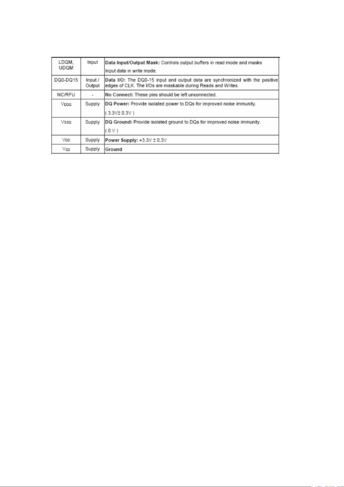
Channel 1 (L’) with one pass band for sound carriers at 40,40 MHz (L’) and 39,75
MHz (L’- NICAM)
Channel 2 (B/G,D/K,L,I) with one pass band for sound carriers between 32,35 MHz
and 33,40 MHz
9.1.3 Pin Configuration
1 Input
2 Switching input
3 Chip carrier - ground
4 Output
5 Output
9.1.4 Frequency Response
Frequency Response of Channel 1:
Frequency Response of Channel 2:
15
Page 17

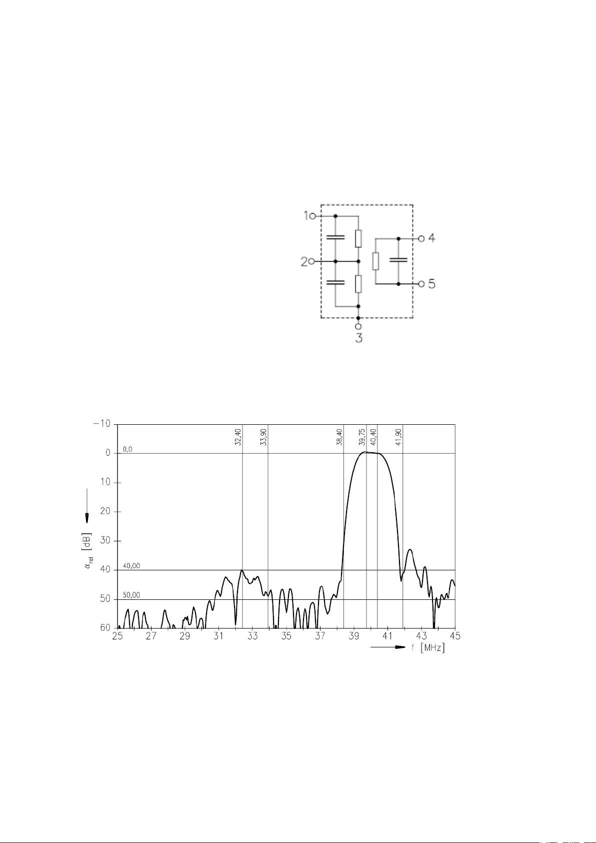
9.2 IF Filter for Video Applications – Epcos K3958M
9.2.1 Standarts
B/G
D/K
I
L/L’
9.2.2 Features
TV IF filter with Nyquist slopes at 33.90 MHz and 38.90 MHz
Constant group delay
9.2.3 Pin Configuration
1 Input
2 Input - ground
3 Chip - carrier ground
4 Output
5 Output
16
Page 18
9.2.4 Frequency Response
10. POWER STAGE
The DC voltages required at various parts of the chassis and inverters are provided by an
external power supply unit or produced on the chassis if an adapter is used for the supply. The
12V dc voltage is switched by IRF 7314 power mosfet in TV sets with mechanical switch to
produce the required standby voltage. Also regulators and mosfets generate 1.8V, 3.3V and
5V and 1.26V voltages for other different parts of the chassis.
17
Page 19

11. IC SPECIFICATIONS
11.1 32K Smart Serial EEPROM – 24C32
General Description
The Microchip Technology Inc. 24C32 is a 4K x 8 (32K bit) Serial Electrically Erasable
PROM. This device has been developed for advanced, low power applications such as
personal communications or data acquisition. The 24C32 features an input cache for fast write
loads with a capacity of eight 8-byte pages, or 64 bytes. It also features a fixed 4K-bit block
of ultra-high endurance memory for data that changes frequently. The 24C32 is capable of
both random and sequential reads up to the 32K boundary. Functional address lines allow up
to eight 24C32 devices on the same bus, for up to 256K bits address space. Advanced CMOS
technology makes this device ideal for low-power non-volatile code and data applications.
The 24C32 is available in the standard 8-pin plastic DIP and 8-pin surface mount SOIC
package.
Features
Voltage operating range: 4.5V to 5.5V
Peak write current 3 mA at 5.5V
Maximum read current 150 µA at 5.5V
Standby current 1 µA typical
Industry standard two-wire bus protocol, I2C compatible
Including 100 kHz and 400 kHz modes
Self-timed write cycle (including auto-erase)
Power on/off data protection circuitry
Endurance: 10,000,000 Erase/Write cycles guaranteed for High Endurance
Block, 1,000,000 E/W cycles guaranteed for Standard Endurance Block
8 byte page, or byte modes available
1 page x 8 line input cache (64 bytes) for fast write loads
Schmitt trigger, filtered inputs for noise suppression
Output slope control to eliminate ground bounce
2 ms typical write cycle time, byte or page
Up to 8 chips may be connected to the same bus for up to 256K bits total
memory
Electrostatic discharge protection > 4000V
Data retention > 200 years
8-pin PDIP/SOIC packages
Temperature ranges: Commercial (C): 0°C to +70°C, Industrial (I): -40°C to
+85°C
18
Page 20
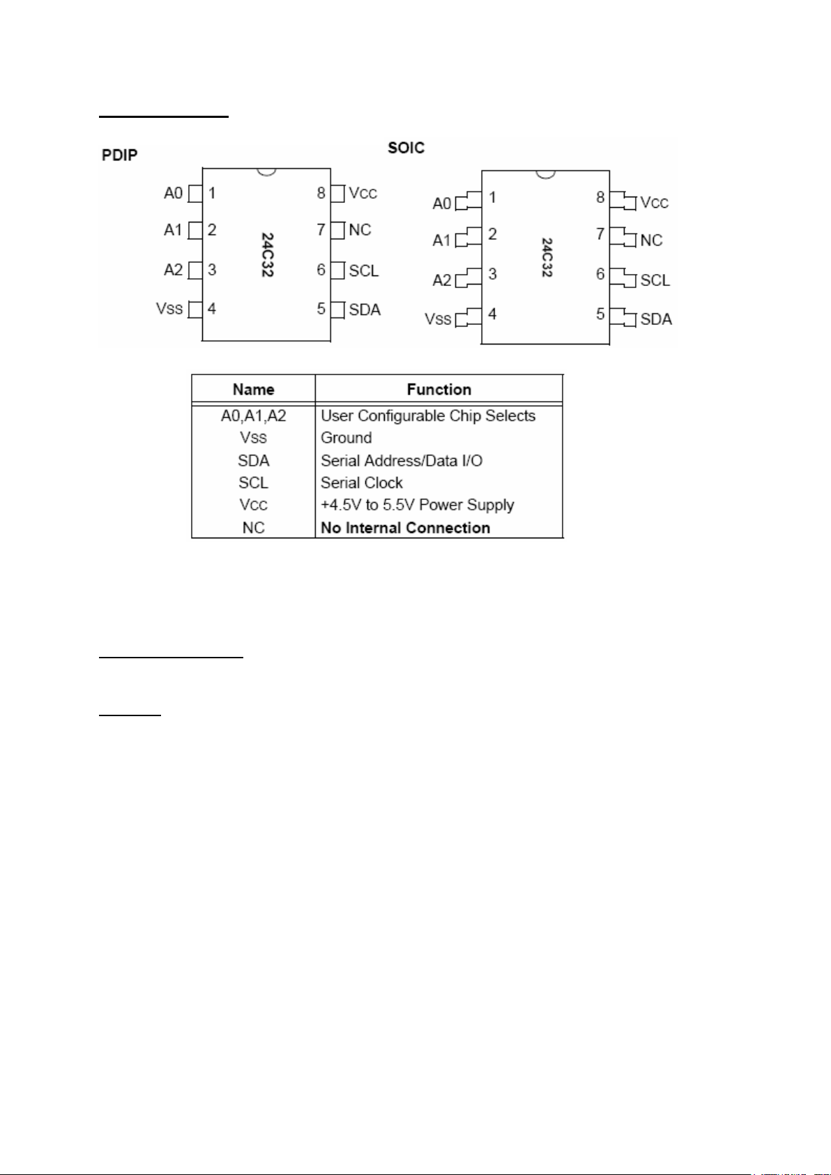
Pin Configuration
11.2 TL062
General Description
Low-power JFET-input operational amplifier
Features
Very Low Power Consumption
Typical Supply Current . . . 200 µA (Per Amplifier)
Wide Common-Mode and Differential Voltage Ranges
Low Input Bias and Offset Currents
Common-Mode Input Voltage Range Includes VCC+
Output Short-Circuit Protection
High Input Impedance . . . JFET-Input Stage
Internal Frequency Compensation
Latch-Up-Free Operation
High Slew Rate . . . 3.5 V/µs Typ
19
Page 21
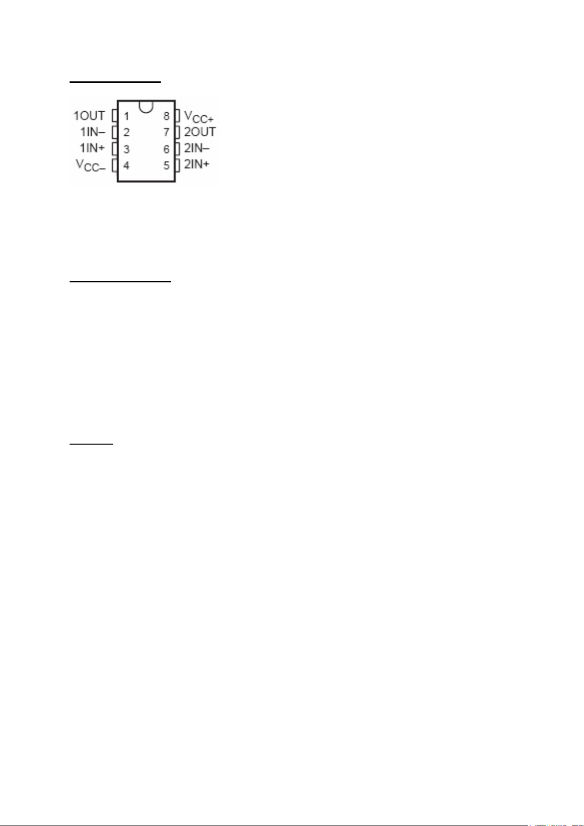
Pin Configuration
11.3 PI5V330
General Description
Pericom Semiconductor.s PI5V series of mixed signal video circuits are produced in the
Company.s advanced CMOS low-power technology, achieving industry leading performance.
The PI5V330 is a true bidirectional Quad 2-channel multiplexer/demultiplexer that is
recommended for both RGB and composite video switching applications. The VideoSwitch.
can be driven from a current output RAMDAC or voltage output composite video source.
Low ON-resistance and wide bandwidth make it ideal for video and other applications. Also
this device has exceptionally high current capability which is far greater than most analog
switches offered today. A single 5V supply is all that is required for operation. The PI5V330
offers a high-performance, low-cost solution to switch between video sources. The application
section describes the PI5V330 replacing the HC4053 multiplier and buffer/amplifier.
Features
High-performance, low-cost solution to switch between video sources
Wide bandwidth: 200 MHz
Low ON-resistance: 3Ω
Low crosstalk at 10 MHz: .58 dB
Ultra-low quiescent power (0.1 µA typical)
Single supply operation: +5.0V
Fast switching: 10 ns
High-current output: 100 mA
Packages available:
16-pin 300-mil wide plastic SOIC (S)
16-pin 150-mil wide plastic SOIC (W)
16-pin 150-mil wide plastic QSOP (Q)
20
Page 22
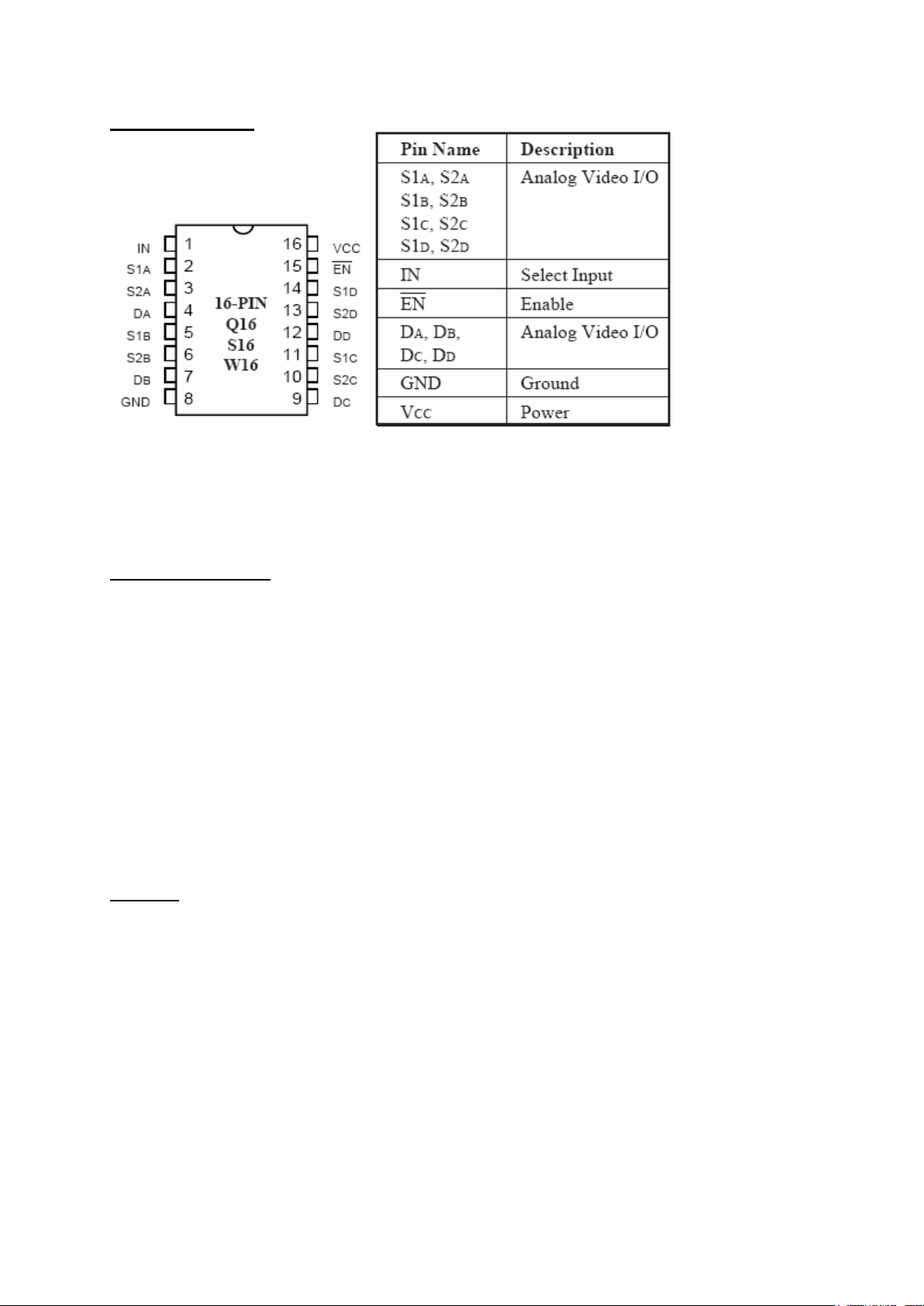
Pin Configuration
11.4 74HCT4053
General Description
The 74HC4053; 74HCT4053 is a high-speed Si-gate CMOS device and is pin compatible
with the HEF4053B. It is specified in compliance with JEDEC standard no. 7A. The
74HC4053; 74HCT4053 is triple 2-channel analog multiplexer/demultiplexer with a common
enable input (E). Each multiplexer/demultiplexer has two independent inputs/outputs (nY0
and nY1), a common input/output (nZ) and three digital select inputs (Sn). With E LOW, one
of the two switches is selected (low-impedance ON-state) by S1 to S3. With E HIGH, all
switches are in the high-impedance OFF-state, independent of S1 to S3. VCC and GND are
the supply voltage pins for the digital control inputs (S1 to S3 and E). The VCC to GND
ranges are 2.0 V to 10.0 V for 74HC4053 and 4.5 V to 5.5 V for 74HCT4053. The analog
inputs/outputs (nY0 and nY1, and nZ) can swing between VCC as a positive limit and VEE as
a negative limit. VCC - VEE may not exceed 10.0 V.
For operation as a digital multiplexer/demultiplexer, VEE is connected to GND (typically
ground).
Features
Low ON resistance:
80 W (typical) at VCC - VEE = 4.5 V
70 W (typical) at VCC - VEE = 6.0 V
60 W (typical) at VCC - VEE = 9.0 V
Logic level translation:
To enable 5 V logic to communicate with ±5 V analog signals
Typical ‘break before make’ built in
Complies with JEDEC standard no. 7A
ESD protection: HBM EIA/JESD22-A114-C exceeds 2000 V, MM EIA/JESD22-
A115-A exceeds 200 V
Multiple package options
Specified from -40 °C to +85 °C and from -40 °C to +125 °C
21
Page 23
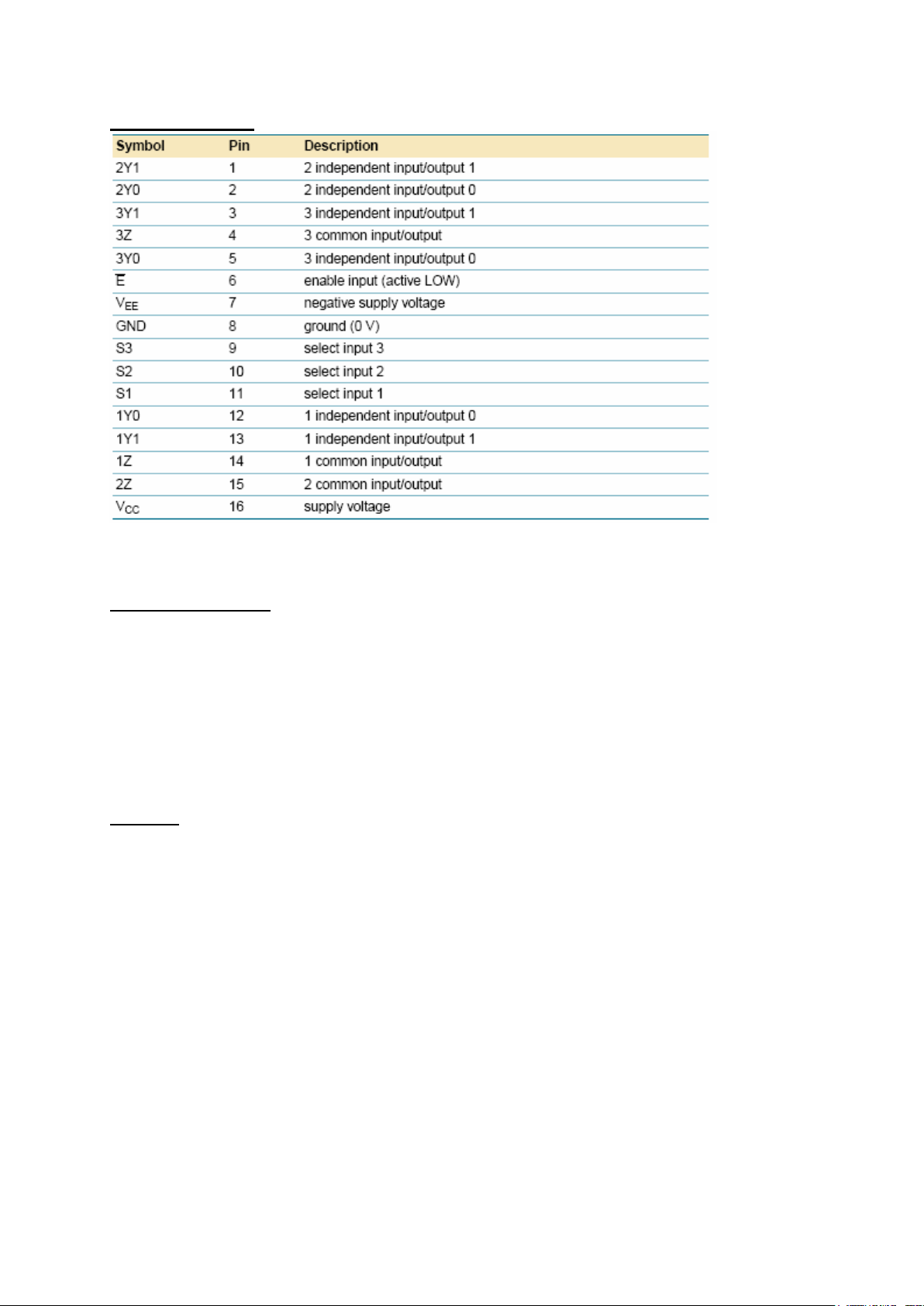
Pin Configuration
11.5 FMS6145
General Description
The FMS6145 Low-Cost Video Filter (LCVF) is intended to replace passive LC fi lters and
drivers with a low-cost integrated device. Five 4th-order fi lters provide improved image
quality compared to typical 2nd or 3rd-order passive solutions. The FMS6145 may be directly
driven by a DC-coupled DAC output or an AC-coupled signal. Internal diode clamps and bias
circuitry may be used if AC-coupled inputs are required. The outputs can drive AC- or DC-
coupled single (150Ω) or dual (75Ω) loads. DC coupling the outputs removes the need for
output coupling capacitors. The input DC levels are offset approximately +280mV at the
output.
Features
Five 4th-order 8MHz (SD) fi lters
Drives single,AC- or DC-coupled, video loads (2Vpp, 150Ω)
Drives dual, AC- or DC-coupled, video loads (2Vpp, 75Ω)
Transparent input clamping
AC- or DC-coupled inputs
AC- or DC-coupled outputs
DC-coupled outputs eliminate AC-coupling capacitors
5V only
Robust 8kV ESD protection
Lead-free TSSOP-14 package
22
Page 24
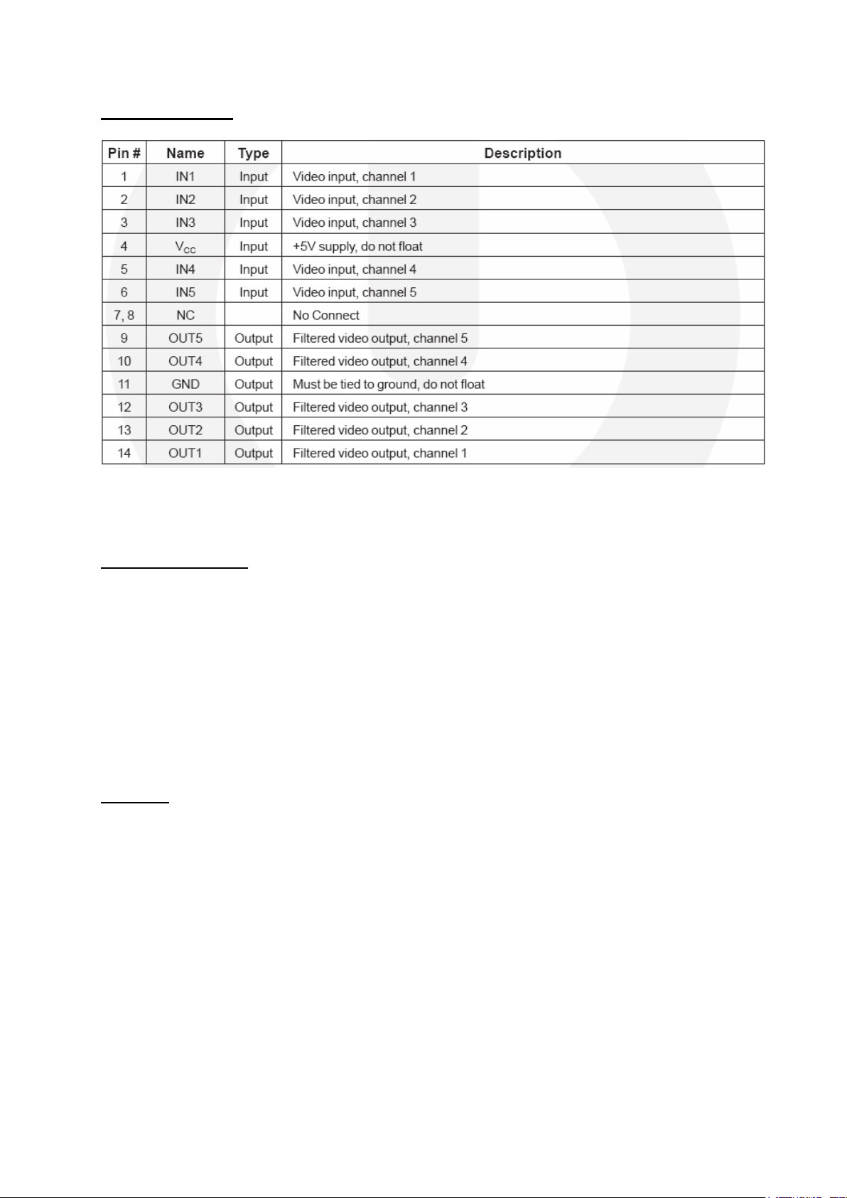
Pin Configuration
11.6 LM1117
General Description
The LM1117 is a series of low dropout voltage regulators with a dropout of 1.2V at 800mA of
load current. It has the same pin-out as National Semiconductor’s industry standard LM317.
The LM1117 is available in an adjustable version, which can set the output voltage from
1.25V to 13.8V with only two external resistors. In addition, it is also available in five fixed
voltages, 1.8V, 2.5V, 2.85V, 3.3V, and 5V. The LM1117 offers current limiting and thermal
shutdown. Its circuit includes a zener trimmed bandgap reference to as-sure output voltage
accuracy to within ±1%. The LM1117 series is available in SOT- 223, TO-220, and TO-252
D-PAK packages. A minimum of 10μF tantalum capacitor is required at the output to improve
the transient response and stability.
Features
Available in 1.8V, 2.5V, 2.85V, 3.3V, 5V, and Adjustable Versions
Space Saving SOT-223 Package
Current Limiting and Thermal Protection
Output Current 800mA
Line Regulation 0.2% (Max)
Load Regulation 0.4% (Max)
Temperature Range
LM1117 0°C to 125°C
LM1117I -40°C to 125°C
23
Page 25

Pin Configuration
11.7 ST24LC21
Description
The ST24LC21 is a 1K bit electrically erasable programmable memory (EEPROM),
organized by 8 Bits.This device can operate in two modes: Transmit Only mode and I2C
bidirectional mode. When powered, the device is in Transmit Only mode with EEPROM data
clocked out from the rising edge of the signal applied on VCLK. The device will switch to the
I2C bidirectional mode upon the falling edge of the signal applied on SCL pin. The
ST24LC21 cannot switch from the I2C bidirectional mode to the Transmit Only mode (except
when the power supply is removed). The device operates with a power supply value as low as
2.5V. Both Plastic Dual-in-Line and Plastic Small Outline packages are available.
Features
1 Mıllıon Erase/Wrıte Cycles
40 Years Data Retentıon
2.5v To 5.5v Sıngle Supply Voltage
400k Hz Compatıbılıty Over The Full
Range Of Supply Voltage
Two Wıre Serıal Interface I2c Bus
Compatıble
Page Wrıte (Up To 8 Bytes)
Byte, Random And Sequentıal Read
Modes
Self Tımed Programmıng Cycle
Automatıc Address Incrementıng
Enhanced Esd/Latch Up
Performances
24
Page 26

Pin Configuration
11.8 24LC02
Description
The Microchip Technology Inc. 24AA02/24LC02B (24XX02*) is a 2 Kbit Electrically
Erasable PROM. The device is organized as one block of 256 x 8-bit memory with a 2-wire
serial interface. Low-voltage design permits operation down to 1.8V, with standby and active
currents of only 1 A and 1 mA, respectively. The 24XX02 also has a page write capability
for up to 8 bytes of data. The 24XX02 is available in the standard 8-pin PDIP, surface mount
OIC, TSSOP and MSOP packages and is also available in the 5-lead SOT-23 package.
Features
• Single supply with operation down to 1.8V
• Low-power CMOS technology
- 1 mA active current typical
- 1µA standby current typical (I-temp)
• Organized as 1 block of 256 bytes (1 x 256 x 8)
• 2-wire serial interface bus, I2C™ compatible
• Schmitt Trigger inputs for noise suppression
• Output slope control to eliminate ground bounce
• 100 kHz (24AA02) and 400 kHz (24LC02B) compatibility
• Self-timed write cycle (including auto-erase)
• Page write buffer for up to 8 bytes
• 2 ms typical write cycle time for page write
• Hardware write-protect for entire memory
• Can be operated as a serial ROM
• Factory programming (QTP) available
• ESD protection > 4,000V
• 1,000,000 erase/write cycles
• Data retention > 200 years
• 8-lead PDIP, SOIC, TSSOP and MSOP packages
• 5-lead SOT-23 package
• Pb-free finish available
• Available for extended temperature ranges:
25
Page 27

- Industrial (I): -40°C to +85°C
- Automotive (E): -40°C to +125°C
Pin Configuration
11.9 MAX810
General Description
The MAX809 and MAX810 are cost-effective system supervisor circuits designed to monitor
VCC in digital systems and provide a reset signal to the host processor when necessary. No
external components are required. The reset output is driven active within 10 _sec of VCC
falling through the reset voltage threshold. Reset is maintained active for a timeout period
which is trimmed by the factory after VCC rises above the reset threshold. The MAX810 has
an active-high RESET output while the MAX809 has an active-low RESET output. Both
devices are available in SOT-23 and SC-70 packages. The MAX809/810 are optimized to
reject fast transient glitches on the VCC line. Low supply current of 0.5 _A (VCC = 3.2 V)
makes these devices suitable for battery powered applications.
Features
Precision VCC Monitor for 1.5 V, 2.5 V, 3.0 V, 3.3 V, and 5.0 V Supplies
Precision Monitoring Voltages from 1.2 V to 4.9 V Available in 100 mV Steps
Four Guaranteed Minimum Power-On Reset Pulse Width Available (1 ms, 20 ms, 100
ms, and 140 ms)
RESET Output Guaranteed to VCC = 1.0 V.
Low Supply Current
Compatible with Hot Plug Applications
VCC Transient Immunity
No External Components
Wide Operating Temperature: -40°C to 105°C
Pb-Free Packages are Available
26
Page 28

Pin Configuration
11.10 TDA1308
Description
The TDA1308 is an integrated class AB stereo headphone driver contained in an SO8 or a
DIP8 plastic package. The device is fabricated in a 1 mm CMOS process and has been
primarily developed for portable digital audio applications.
Features
Operating temperature range: -40 to +85 C
No switch ON/OFF clicks
Short-circuit resistant
signal-to-noise ratio: 110 dB
total harmonic distortion: 0.001 %
Pin Configuration
11.11 MP1583
General Description
The MP1583 is a step-down regulator with a built in internal Power MOSFET. It achieves 3A
continuous output current over a wide input supply range with excellent load and line
regulation. Current mode operation provides fast transient response and eases loop
stabilization. Fault condition protection includes cycle-by-cycle current limiting and thermal
27
Page 29

shutdown. Adjustable soft-start reduces the stress on the input source at turn-on. In shutdown
mode the regulator draws 20µA of supply current.
The MP1583 requires a minimum number of readily available external components to
complete a 3A step down DC to DC converter solution.
Features
3A Output Current
Programmable Soft-Start
100mΩ Internal Power MOSFET Switch
Stable with Low ESR Output Ceramic Capacitors
Up to 95% Efficiency
20µA Shutdown Mode
Fixed 385KHz frequency
Thermal Shutdown
Cycle-by-Cycle Over Current Protection
Wide 4.75 to 23V operating Input Range
Output Adjustable From 1.22 to 21V
Under Voltage Lockout
Available in 8 pin SOIC Package
3A Evaluation Board Available
Pin Configuration
28
Page 30

11.12 MP2112
General Description
The MP2112 is a 1MHz constant frequency, current mode, PWM step-down converter. The
device integrates a main switch and a synchronous rectifier for high efficiency without an
external Schottky diode. It is ideal for powering portable equipment that powered by a single
cell Lithium-Ion (Li+) battery. The MP2112 can supply 1A of load current from a 2.5V to 6V
input voltage. The output voltage can be regulated as low as 0.6V. The MP2112 can also run
at 100% duty cycle for low dropout applications.
The MP2112 is available in a space-saving 6-pin QFN package
Features
High Efficiency: Up to 95%
1MHz Constant Switching Frequency
1A Available Load Current
2.5V to 6V Input Voltage Range
Output Voltage as Low as 0.6V
100% Duty Cycle in Dropout
Current Mode Control
Short Circuit Protection
Thermal Fault Protection
<0.1µA Shutdown Current
Space Saving 3mm x 3mm QFN6 Package
.
Pin Configuration
11.13 IRF7314
General Description
Fifth Generation HEXFETs from International Rectifier utilize advanced processing
techniques to achieve extremely low on-resistance per silicon area. This benefit, combined
with the fast switching speed and ruggedized device design that HEXFET Power MOSFETs
are well known for, provides the designer with an extremely efficient and reliable device for
use in a wide variety of applications. The SO-8 has been modified through a customized
leadframe for enhanced thermal characteristics and multiple-die capability making it ideal in a
variety of power applications. With these improvements, multiple devices can be used in an
application with dramatically reduced board space. The package is designed for vapor phase,
infra red, or wave soldering techniques.
29
Page 31

Pin Configuration
12. SERVICE MENU SETTINGS
In order to reach service menu, First Press “MENU” Then press the remote control
code, which is “4725”. In DTV mode, first press “MENU” and select “TV SETUP”.
Then, press “4725”.
12.1. Video Setup
Panel Info <..................................>
32_LC_SAC1
Blue Background <.....>
If “Menu” selected, “Blue Background” item is seen in “Feature”
menu.
If “Yes” selected, “Blue Background” is on and not seen in
“Feature” menu
Film Mode <.....>
If “Yes” selected, “Film Mode” feature is active.
Dynamic Contrast <.....>
If “Yes” selected, “Dynamic Contrast” feature is active.
Game Mode <...........>
If “Yes” selected, “Game Mode” feature is active
SRGB For PC <...........>
If “Yes” selected, PCs can use SRGB option.
Dynamic Noise Reduction<...........>
If “Yes” selected, “Dynamic Noise Reduction” feature is active
WSS Option<...........>
If “Yes” selected, WSS Option can be used
12.2. AudioSetup
BG<.....>
Europe
30
Page 32

New Zelland
Australia
No
DK<.....>
I<.....>
L<.....>
Equalizer <.....>
If “Yes” selected, “Equalizer” item is seen in “Sound” menu.
Headphone <.....>
If “Yes” selected, “Headphone” item is seen in “Sound” menu.
Power On/Off Melody <.....>
If “Yes” selected, when power on/off conditions, the power on/off
melody can be heard.
Dynamic Bass <.....>Value between 0 to 12
Effect<.....> Value between 0 to 7
Audio Delay ,offset <.....> Value between 0 to 190
Audio Setup Cont...2
Carrier mute<.......>
Value between 0 to 28
Headphone Sound Select <.......>
Always Active Select
Always Inactive Select
Menu
Always Main Menu
Always PIP/PAP Window
Sound Mode Detect Time <.......>
Value between 0 to 255
Noise Reduction Threshold <.......> Value between 0 to 255
Noise Reduction Time <.......> Value between 0 to 15
AVL Attack Time <.......> Value between 0 to 255
AVL Release Time <.......> Value between 0 to 255
Prescales ( AVL On)
FM Prescale<.......>
Value between 0 to 255
AM Prescale <.......> Value between 0 to 255
NICAM Prescale <.......> Value between 0 to 255
SCART Prescale <.......> Value between 0 to 255
FAV Prescale <.......> Value between 0 to 255
DTV Prescale <.......> Value between 0 to 255
HDMI Prescale <.......> Value between 0 to 255
YPbPr/PC Prescale <.......> Value between 0 to 255
An. USB Prescale <.......> Value between 0 to 255
Dig. USB Prescale <.......> Value between 0 to 255
Prescales ( AVL Off)
FM Prescale<.......>
Value between 0 to 255
AM Prescale <.......> Value between 0 to 255
NICAM Prescale <.......> Value between 0 to 255
SCART Prescale <.......> Value between 0 to 255
FAV Prescale <.......> Value between 0 to 255
DTV Prescale <.......> Value between 0 to 255
HDMI Prescale <.......> Value between 0 to 255
YPbPr/PC Prescale <.......> Value between 0 to 255
Page 33

An. USB Prescale <.......> Value between 0 to 255
Dig. USB Prescale <.......> Value between 0 to 255
Clipping Levels ( AVL On)
FM Clipping <.......>
AM Clipping <.......> Value between 0 to 255
NICAM Clipping <.......> Value between 0 to 255
SCART Clipping <.......> Value between 0 to 255
FAV Clipping <.......> Value between 0 to 255
DTV Clipping <.......> Value between 0 to 255
HDMI Clipping <.......> Value between 0 to 255
YPbPr/PC Clipping <.......> Value between 0 to 255
An. USB Clipping <.......> Value between 0 to 255
Dig. USB Clipping <.......> Value between 0 to 255
Clipping Levels ( AVL Off)
FM Clipping <.......>
AM Clipping <.......> Value between 0 to 255
NICAM Clipping <.......> Value between 0 to 255
SCART Clipping <.......> Value between 0 to 255
FAV Clipping <.......> Value between 0 to 255
DTV Clipping <.......> Value between 0 to 255
HDMI Clipping <.......> Value between 0 to 255
YPbPr/PC Clipping <.......> Value between 0 to 255
An. USB Clipping <.......> Value between 0 to 255
Dig. USB Clipping <.......> Value between 0 to 255
Value between 0 to 255
Value between 0 to 255
12.3. Service Scan/Tuning Setup
First Search for L/L’ <.......>
ATS Delay Time (ms) <.......> Value between 0 to +200
Main Tuner Setup
Tuner Type
LC_TDTC_GXX1D
Thomson DTT7543X
Philips TD1318AF-3
Samsung DTOs403LH172A
Generic ( Analog Only)
Control Byte <.......>
BSW1 <.......> Value between 0 to +255
BSW2 <.......> Value between 0 to +255
BSW3 <.......> Value between 0 to +255
Low-Mid – Low Byte <.......>
Low-Mid – High Byte <.......>
Mid-High – Low Byte <.......>
Mid-High – High Byte <.......>
S Band TOP <.......>
VIF TOP <.......> Value between 0 to +15
VIF TOP SECAM <.......> Value between 0 to +15
VIF TOP DK<.......> Value between 0 to +15
Synch Threshold<.......> Value between 0 to +40
Value between 0 to +255
Page 34

16.4. Options
Options-1
Power Up
Standby
Last state
TV Open Mode
Source
1st TV
Last Tv
First APS <.......>
APS Volume <.......> Value between 0 to +63
Burn In Mode <.......>
used in manufacturing.
APS Test
Autostore <.......>
Unicode Enabled <.......>
Files.
Options-2
Source List menu <.......>
when press “source” button.
RS232 for B2B <.......>
RS232 and vice versa.
RC Select <.......>
RC Group 1
RC Group 2
RC Group 3
RC Group 4
RC Group 5
RC Group 6
Double Digit Key <.......>
Protection <.......>
Led Type <.......>
1 Led 1 Color
1 Led 2 Color
2 Led 2 Color
1 Led 3 Color
2 Led 3 Color
200 Programme <.......>
If “Yes” selected, totaly 200 programmes can be used.
TouchPad <.......>
If “Yes” selected, TouchPad can be used.
If “Yes” selected, first time TV opens by asking APS.
If “Yes” selected, TV opens with Burn-In mode. This mode is
If “Yes” selected, Channel is automatically stored.
If “Yes” selected,Unicode characters can be read in the USB
If “Yes” selected, Sorce List Menu appears on the screen
If “Yes” selected, Remote Control commandsthe TV via
If “Yes” selected, Double Digit Button on RC activates.
If “Yes” selected,short circuit protection activates.
Page 35

Teletext Options
TXT Darkness <.......>
TXT Type <.......>
TXT Language <.......>
No Txt Warning <.......>
Txt Subtitle <.......>
Optional Features
Default Zoom <.......>
Menu Timeout <.......>
Backlight <.......>
100 Step Slider <.......>
Analog USB Enabled <.......>
Menu Double Size <.......>
CEC Enable <.......>
Digital USB Hotplug <.......>
Value between 0 to +63
Fasttext&Toptext
No
Default
Fastext
Toptext
Menu
West
East
Cyrillic
Turk/Gre
Arabic
Persian
Auto
If “Yes” selected, “No Txt Transmission” warning appears on
the screen when pressing txt button from RC.
If “Yes” selected, Teletext subtitles can be seen.
Menu
16:9
4:3
Panaromic
14:9 Zoom
Menu
15 Sec
30 Sec
60 Sec
No Time
If “Yes” selected, “Backlight” feature is active.
If “Yes” selected, 64 step sliders will become 100 step sliders.
If “Yes” selected, “Analog USB” option is active.
If “Yes” selected, menu sizes increases.
If “Yes” selected, “CEC” feature is active.
If “Yes” selected, “Digital USB Hotplug” feature is active.
Page 36

PIP Options
Pip <......>
AV PIP
No PIP
PC PIP
Hotel Options <......>
Hotel TV <......>
If “Yes” selected, “Hotel TV” feature is active.
IR Smartloader <......>
If “Yes” selected, “IR Smartloader” feature is active.
16.5. External Source Settings
TV <.......>
DTV <.......>
Ext 2 <.......>
Ext 2 S <.......>
FAV <.......>
BAV <.......>
S-Video <.......>
HDMI 1 <.......>
HDMI 2 <.......>
HDMI 3 <.......>
HDMI 4 <.......>
YPbPr <.......>
PC <.......>
16.6. Preset
User Ad.j
ADC Adj.
Service Adj.
All Adj.
Init Factory Channels.
16.7. NVM Edit
NVM-edit addr. (hex)
NVM-edit data (hex)
NVM-data dec
16.8. Programming
HDMI DDC Update Mode <.......>
HDCP Key Update Mode <.......>
Software Bypass <.......>
If “On” selected, speaker effects are bypassed.
LVDS Clock Step <.......> Value between 0 to +255
Memory Clock Step <.......> Value between 0 to +255
DTV Download <.......>
If “On” selected, DTV software can be updated from SCART.
Page 37

DSUB9 Download <.......>
If “On” selected, DTV software can be updated from DSUB9.
16.9. Diagnostic
Eeprom I2C
Tuner I2C
IF I2C
HDMI I2C
DTV RS232
16.10. Product Info
13. SOFTWARE UPDATE DESCRIPTION
13.1 17MB25 Analog Part Software Update With Bootloader Procedure
1.1 The File Types Used By The Bootloader
All file types that used by the bootloader software are listed below:
1. The Binary File : It has “.bin” extension and it is the tv application. Its size is 1920
Kb.
2. The Config Binary File : It has “.cin extension and it is the config of the tv
application. Its size may be 64 Kb or a few times 64 Kb.
3. The Test Script File : It has “.txt” extension and it is the test script that is parsed
and executed by the bootloader. It don’t have to be any times of 64 Kb.
4. The Test Binary File : It has “.tin” extension and it is used and written by the test
groups. It is run to understand the problem part of the hardware.
Alltough a file that is used by the bootloader can be had any one of these extensions, its
name has to be “VESTEL_S” and it has to be located in the root directory of the usb
device.
1.2 Usage of The Bootloader
1. The starting to pass through : The chassis is only powered up.
2. The starting to download something : When chassis is powered up the menu key has
to be pushed.Before the chassis is powered up and if any usb device is plugged to the
usb port, the programme is downloaded from usb firstly.
Any usb device is plugged to usb port , user must open hyperterminal in the pc and
connect pc to chassis via Mstar debug tool and any one of scart,dsub9 or I2c
connectors. Serial connection settings are listed below:
- Bit per second: 115200
- Data bits: 8
Page 38

- Parity: None
- Stop bits: 1
- Flow control: None
In this case the bootloader sofware puts “C” character to uart. After repeating “C”
characters are seen in the hyperterminal user can send any file to chassis by selecting
Transfer -> Send File menu item and choosing “
1K Xmodem” from protocol section.
Figure 1. The Sample Output Before Sending The File
2. EEProm update
To Update eeprom content via uart scart,dsub9 or i2c with Mstar tool can used.
Serial connection settings are listed below:
- Bit per second: 9600
- Data bits: 8
- Parity: None
- Stop bits: 1
- Flow control: None
Programming menu item is choosed in the service menu and switch “HDCP Key Update
Mode” from off to on.
Page 39

Figure 2. The Programming Service Menu
After then you must see Xmodem menu in the hyperterminal.To download hdcp key
press k or to download eeprom content press w.
Figure 3. Xmodem Menu
If the repeated “C” characters are seen you can transfer file content via select Transfer>Send File and choose “
Xmodem” protocol and click the “Send” button.
Page 40

Figure 4. The Starting To Send
16.2 17MB25 HDCP key upload procedure.
1) Turn on TV set.
2) Open a COM connection using fallowing parameters and select ISP COM Port
No
Baud Rate: 9600 bps
Data Bits: 8
Stop Bits: 1
Parity: None
Flow Control: None
3) Enter service menu by pressing “4” “7” “2” 5” consecutively while main menu is
open
4) Select “9. Programming”
5) Select “HDMI HDCP Update Mode” yes.
6) On Hyper Terminal Window press “k”
7) Click on send file under Transfer Tab.
8) Select Xmodem and choose the HDCP key to be uploaded.
9) Press send button
10)Restart TV set
Page 41

13.3 17MB25 Digital Software Update From SCART
Adjusting DTV Download Mode:
1. Power on the TV.
2. Exit the Stby Mode.
3. Enter the “Tv Menu”.
4. Enter “4725” for jumping to “Service Settings”.
5. Select “8. Programming” step.
6. Change “6. DTV Download” to “On”.
7. Switch to the Stby mode.
Adjusting HyperTerminal:
1. Connect the “MB25 SCART Interface” to SCART1 (bottom SCART plug).
2. Also connect the “MB25 SCART Interface” to PC.
3. Open “HyperTerminal”.
4. Determine the “COM” settings listed and showed below.
Bit per second: 115200
Data bits: 8
Parity: None
Stop bits: 1
Flow control: None
6. Click “OK”.
COM Properties Window
Page 42

Software Updating Procedure
1. In the HyperTerminal Menu, click the “Connect” button.
2. Exit the Stby Mode.
3. The “Space” button on the keyboard must be pressed, when the following window can
be seen.
Selection Window
4. Press the “2” button on the keyboard for choosing “2. Upgrade Application with
Xmodem”.
5. Repeating “C” characters are seen in the “HyperTerminal” menu.
The Sample Output Before Sending The File
Page 43

6. Click the “Send” button on the HyperTerminal
7. Select the “Filename
xxxx_slot1.img” using “Browse”.
8. Choose the “1K Xmodem” from “Protocol” option.
Selection of File
File and Protocol Selection Window
Note: In the Software updating Procedure section, when the first “C” character is seen,
the filename selection process must be finished before 10 seconds. If the process can
not be finished, the file sending operation will be cancelled. The following figure shows
this situation.
Page 44

Capture of Receving Data Failing
9. When sending the file the following window must be seen.
Capture of Sending Process
10. After the sending process the following HyperTerminal window must be seen.
Page 45

Capture of End of The Sending Process
11. For sending second program file, the Software Updating Procedure must be
repeated from the step
X. Select the “Filename xxxx_slot2.img” using “Browse”.
12. After sending the second program file, the Software Updating Procedure will be
succesful.
Note: After the File Sending Process,
1. Upgrade Application with FUM
2. Upgrade Application with Xmodem, options must be seen.
End of The Sending Process
Page 46

Checking Of The New Software
1. Turn off and on the TV.
2. Enter the “Setup” submenu in the “DTV Menu”.
3. Choose the “Configuration” option.
4. For controlling new software, check the “Receiver Upgrade” option.
13.4 17MB25 Digital Software Update From USB
Software upgrade is possible via USB disk by folowing the steps below.
1. Copy the bin file, including higher version than the software loaded in flash, into
the USB flash memory root directory. This file should be named up.bin.
2. Insert the USB disk.
3. Digital module performs version and CRC check. If version and CRC check is
successful, then a message prompt appears to notify user about new version. If
the user confirms loading of new version, upgrade.bin file is written into flash
unused slot.
4. Digital module disables the previous software in the flash and then a system
reset is performed.
5. After the reset, digital module starts with new software.
Revert operation:
With revert operation, it is possible to downgrade the software.
Revert operation is very similar to upgrade process. In the revert operation, file name
should be f_up.bin. Also user confirmation is not asked.
1. Copy the bin file into the USB flash memory root directory. This file should be
named force_upgrade.bin.
2. Insert the USB disk.
3. A lower version than the software in flash can be loaded with revert operation.
Digital module performs only CRC check. If CRC check is successful, then
force_upgrade.bin file is written into flash unused slot.
4. Digital module disables the previous software in the flash.
5. A message prompt is displayed to notify user about end of revert process.
6. Power off/on is required to start digital module with the new software.
For controlling new software, check the “Receiver Upgrade” option.
Page 47

New Zelland
Australia
No
DK<.....>
I<.....>
L<.....>
Equalizer <.....>
If “Yes” selected, “Equalizer” item is seen in “Sound” menu.
Headphone <.....>
If “Yes” selected, “Headphone” item is seen in “Sound” menu.
Power On/Off Melody <.....>
If “Yes” selected, when power on/off conditions, the power on/off
melody can be heard.
Dynamic Bass <.....>Value between 0 to 12
Effect<.....> Value between 0 to 7
Audio Delay ,offset <.....> Value between 0 to 190
Audio Setup Cont...2
Carrier mute<.......>
Value between 0 to 28
Headphone Sound Select <.......>
Always Active Select
Always Inactive Select
Menu
Always Main Menu
Always PIP/PAP Window
Sound Mode Detect Time <.......>
Value between 0 to 255
Noise Reduction Threshold <.......> Value between 0 to 255
Noise Reduction Time <.......> Value between 0 to 15
AVL Attack Time <.......> Value between 0 to 255
AVL Release Time <.......> Value between 0 to 255
Prescales ( AVL On)
FM Prescale<.......>
Value between 0 to 255
AM Prescale <.......> Value between 0 to 255
NICAM Prescale <.......> Value between 0 to 255
SCART Prescale <.......> Value between 0 to 255
FAV Prescale <.......> Value between 0 to 255
DTV Prescale <.......> Value between 0 to 255
HDMI Prescale <.......> Value between 0 to 255
YPbPr/PC Prescale <.......> Value between 0 to 255
An. USB Prescale <.......> Value between 0 to 255
Dig. USB Prescale <.......> Value between 0 to 255
Prescales ( AVL Off)
FM Prescale<.......>
Value between 0 to 255
AM Prescale <.......> Value between 0 to 255
NICAM Prescale <.......> Value between 0 to 255
SCART Prescale <.......> Value between 0 to 255
FAV Prescale <.......> Value between 0 to 255
DTV Prescale <.......> Value between 0 to 255
HDMI Prescale <.......> Value between 0 to 255
YPbPr/PC Prescale <.......> Value between 0 to 255
Page 48

An. USB Prescale <.......> Value between 0 to 255
Dig. USB Prescale <.......> Value between 0 to 255
Clipping Levels ( AVL On)
FM Clipping <.......>
AM Clipping <.......> Value between 0 to 255
NICAM Clipping <.......> Value between 0 to 255
SCART Clipping <.......> Value between 0 to 255
FAV Clipping <.......> Value between 0 to 255
DTV Clipping <.......> Value between 0 to 255
HDMI Clipping <.......> Value between 0 to 255
YPbPr/PC Clipping <.......> Value between 0 to 255
An. USB Clipping <.......> Value between 0 to 255
Dig. USB Clipping <.......> Value between 0 to 255
Clipping Levels ( AVL Off)
FM Clipping <.......>
AM Clipping <.......> Value between 0 to 255
NICAM Clipping <.......> Value between 0 to 255
SCART Clipping <.......> Value between 0 to 255
FAV Clipping <.......> Value between 0 to 255
DTV Clipping <.......> Value between 0 to 255
HDMI Clipping <.......> Value between 0 to 255
YPbPr/PC Clipping <.......> Value between 0 to 255
An. USB Clipping <.......> Value between 0 to 255
Dig. USB Clipping <.......> Value between 0 to 255
Value between 0 to 255
Value between 0 to 255
16.3. Service Scan/Tuning Setup
First Search for L/L’ <.......>
ATS Delay Time (ms) <.......>
Main Tuner Setup
Tuner Type
LC_TDTC_GXX1D
Thomson DTT7543X
Philips TD1318AF-3
Samsung DTOs403LH172A
Generic ( Analog Only)
Control Byte <.......>
BSW1 <.......> Value between 0 to +255
BSW2 <.......> Value between 0 to +255
BSW3 <.......> Value between 0 to +255
Low-Mid – Low Byte <.......>
Low-Mid – High Byte <.......>
Mid-High – Low Byte <.......>
Mid-High – High Byte <.......>
S Band TOP <.......>
VIF TOP <.......>
VIF TOP SECAM <.......> Value between 0 to +15
VIF TOP DK<.......> Value between 0 to +15
Synch Threshold<.......> Value between 0 to +40
Value between 0 to +15
Value between 0 to +200
Value between 0 to +255
Page 49

16.4. Options
Options-1
Power Up
Standby
Last state
TV Open Mode
Source
1st TV
Last Tv
First APS <.......>
APS Volume <.......> Value between 0 to +63
Burn In Mode <.......>
used in manufacturing.
APS Test
Autostore <.......>
Unicode Enabled <.......>
Files.
Options-2
Source List menu <.......>
when press “source” button.
RS232 for B2B <.......>
RS232 and vice versa.
RC Select <.......>
RC Group 1
RC Group 2
RC Group 3
RC Group 4
RC Group 5
RC Group 6
Double Digit Key <.......>
Protection <.......>
Led Type <.......>
1 Led 1 Color
1 Led 2 Color
2 Led 2 Color
1 Led 3 Color
2 Led 3 Color
200 Programme <.......>
If “Yes” selected, totaly 200 programmes can be used.
TouchPad <.......>
If “Yes” selected, TouchPad can be used.
If “Yes” selected, first time TV opens by asking APS.
If “Yes” selected, TV opens with Burn-In mode. This mode is
If “Yes” selected, Channel is automatically stored.
If “Yes” selected,Unicode characters can be read in the USB
If “Yes” selected, Sorce List Menu appears on the screen
If “Yes” selected, Remote Control commandsthe TV via
If “Yes” selected, Double Digit Button on RC activates.
If “Yes” selected,short circuit protection activates.
Page 50

Teletext Options
TXT Darkness <.......>
TXT Type <.......>
TXT Language <.......>
No Txt Warning <.......>
Txt Subtitle <.......>
Optional Features
Default Zoom <.......>
Menu Timeout <.......>
Backlight <.......>
100 Step Slider <.......>
Analog USB Enabled <.......>
Menu Double Size <.......>
CEC Enable <.......>
Digital USB Hotplug <.......>
Value between 0 to +63
Fasttext&Toptext
No
Default
Fastext
Toptext
Menu
West
East
Cyrillic
Turk/Gre
Arabic
Persian
Auto
If “Yes” selected, “No Txt Transmission” warning appears on
the screen when pressing txt button from RC.
If “Yes” selected, Teletext subtitles can be seen.
Menu
16:9
4:3
Panaromic
14:9 Zoom
Menu
15 Sec
30 Sec
60 Sec
No Time
If “Yes” selected, “Backlight” feature is active.
If “Yes” selected, 64 step sliders will become 100 step sliders.
If “Yes” selected, “Analog USB” option is active.
If “Yes” selected, menu sizes increases.
If “Yes” selected, “CEC” feature is active.
If “Yes” selected, “Digital USB Hotplug” feature is active.
Page 51

PIP Options
Pip <......>
AV PIP
No PIP
PC PIP
Hotel Options <......>
Hotel TV <......>
If “Yes” selected, “Hotel TV” feature is active.
IR Smartloader <......>
If “Yes” selected, “IR Smartloader” feature is active.
16.5. External Source Settings
TV <.......>
DTV <.......>
Ext 2 <.......>
Ext 2 S <.......>
FAV <.......>
BAV <.......>
S-Video <.......>
HDMI 1 <.......>
HDMI 2 <.......>
HDMI 3 <.......>
HDMI 4 <.......>
YPbPr <.......>
PC <.......>
16.6. Preset
User Ad.j
ADC Adj.
Service Adj.
All Adj.
Init Factory Channels.
16.7. NVM Edit
NVM-edit addr. (hex)
NVM-edit data (hex)
NVM-data dec
16.8. Programming
HDMI DDC Update Mode <.......>
HDCP Key Update Mode <.......>
Software Bypass <.......>
If “On” selected, speaker effects are bypassed.
LVDS Clock Step <.......> Value between 0 to +255
Memory Clock Step <.......> Value between 0 to +255
DTV Download <.......>
If “On” selected, DTV software can be updated from SCART.
Page 52

DSUB9 Download <.......>
If “On” selected, DTV software can be updated from DSUB9.
16.9. Diagnostic
Eeprom I2C
Tuner I2C
IF I2C
HDMI I2C
DTV RS232
16.10. Product Info
17. SOFTWARE UPDATE DESCRIPTION
16.1 17MB25 Analog Part Software Update With Bootloader Procedure
1.1 The File Types Used By The Bootloader
All file types that used by the bootloader software are listed below:
1. The Binary File : It has “.bin” extension and it is the tv application. Its size is 1920
Kb.
2. The Config Binary File : It has “.cin extension and it is the config of the tv
application. Its size may be 64 Kb or a few times 64 Kb.
3. The Test Script File : It has “.txt” extension and it is the test script that is parsed
and executed by the bootloader. It don’t have to be any times of 64 Kb.
4. The Test Binary File : It has “.tin” extension and it is used and written by the test
groups. It is run to understand the problem part of the hardware.
Alltough a file that is used by the bootloader can be had any one of these extensions, its
name has to be “VESTEL_S” and it has to be located in the root directory of the usb
device.
1.2 Usage of The Bootloader
1. The starting to pass through : The chassis is only powered up.
2. The starting to download something : When chassis is powered up the menu key has
to be pushed.Before the chassis is powered up and if any usb device is plugged to the
usb port, the programme is downloaded from usb firstly.
Any usb device is plugged to usb port , user must open hyperterminal in the pc and
connect pc to chassis via Mstar debug tool and any one of scart,dsub9 or I2c
connectors. Serial connection settings are listed below:
- Bit per second: 115200
- Data bits: 8
Page 53

- Parity: None
- Stop bits: 1
- Flow control: None
In this case the bootloader sofware puts “C” character to uart. After repeating “C”
characters are seen in the hyperterminal user can send any file to chassis by selecting
Transfer -> Send File menu item and choosing “
1K Xmodem” from protocol section.
Figure 1. The Sample Output Before Sending The File
2. EEProm update
To Update eeprom content via uart scart,dsub9 or i2c with Mstar tool can used.
Serial connection settings are listed below:
- Bit per second: 9600
- Data bits: 8
- Parity: None
- Stop bits: 1
- Flow control: None
Programming menu item is choosed in the service menu and switch “HDCP Key Update
Mode” from off to on.
Page 54

Figure 2. The Programming Service Menu
After then you must see Xmodem menu in the hyperterminal.To download hdcp key
press k or to download eeprom content press w.
Figure 3. Xmodem Menu
If the repeated “C” characters are seen you can transfer file content via select Transfer>Send File and choose “
Xmodem” protocol and click the “Send” button.
Page 55

Figure 4. The Starting To Send
16.2 17MB25 HDCP key upload procedure.
1) Turn on TV set.
2) Open a COM connection using fallowing parameters and select ISP COM Port
No
Baud Rate: 9600 bps
Data Bits: 8
Stop Bits: 1
Parity: None
Flow Control: None
3) Enter service menu by pressing “4” “7” “2” 5” consecutively while main menu is
open
4) Select “9. Programming”
5) Select “HDMI HDCP Update Mode” yes.
6) On Hyper Terminal Window press “k”
7) Click on send file under Transfer Tab.
8) Select Xmodem and choose the HDCP key to be uploaded.
9) Press send button
10)Restart TV set
Page 56

16.3 17MB25 Digital Software Update From SCART
Adjusting DTV Download Mode:
1. Power on the TV.
2. Exit the Stby Mode.
3. Enter the “Tv Menu”.
4. Enter “4725” for jumping to “Service Settings”.
5. Select “8. Programming” step.
6. Change “6. DTV Download” to “On”.
7. Switch to the Stby mode.
Adjusting HyperTerminal:
1. Connect the “MB25 SCART Interface” to SCART1 (bottom SCART plug).
2. Also connect the “MB25 SCART Interface” to PC.
3. Open “HyperTerminal”.
4. Determine the “COM” settings listed and showed below.
Bit per second: 115200
Data bits: 8
Parity: None
Stop bits: 1
Flow control: None
6. Click “OK”.
COM Properties Window
Page 57

Software Updating Procedure
1. In the HyperTerminal Menu, click the “Connect” button.
2. Exit the Stby Mode.
3. The “Space” button on the keyboard must be pressed, when the following window can
be seen.
Selection Window
4. Press the “2” button on the keyboard for choosing “2. Upgrade Application with
Xmodem”.
5. Repeating “C” characters are seen in the “HyperTerminal” menu.
The Sample Output Before Sending The File
Page 58

6. Click the “Send” button on the HyperTerminal
7. Select the “Filename
xxxx_slot1.img” using “Browse”.
8. Choose the “1K Xmodem” from “Protocol” option.
Selection of File
File and Protocol Selection Window
Note: In the Software updating Procedure section, when the first “C” character is seen,
the filename selection process must be finished before 10 seconds. If the process can
not be finished, the file sending operation will be cancelled. The following figure shows
this situation.
Page 59

Capture of Receving Data Failing
9. When sending the file the following window must be seen.
Capture of Sending Process
10. After the sending process the following HyperTerminal window must be seen.
Page 60

Capture of End of The Sending Process
11. For sending second program file, the Software Updating Procedure must be
repeated from the step
X. Select the “Filename xxxx_slot2.img” using “Browse”.
12. After sending the second program file, the Software Updating Procedure will be
succesful.
Note: After the File Sending Process,
1. Upgrade Application with FUM
2. Upgrade Application with Xmodem, options must be seen.
End of The Sending Process
Page 61

Checking Of The New Software
1. Turn off and on the TV.
2. Enter the “Setup” submenu in the “DTV Menu”.
3. Choose the “Configuration” option.
4. For controlling new software, check the “Receiver Upgrade” option.
16.4 17MB25 Digital Software Update From USB
Software upgrade is possible via USB disk by folowing the steps below.
1. Copy the bin file, including higher version than the software loaded in flash, into
the USB flash memory root directory. This file should be named up.bin.
2. Insert the USB disk.
3. Digital module performs version and CRC check. If version and CRC check is
successful, then a message prompt appears to notify user about new version. If
the user confirms loading of new version, upgrade.bin file is written into flash
unused slot.
4. Digital module disables the previous software in the flash and then a system
reset is performed.
5. After the reset, digital module starts with new software.
Revert operation:
With revert operation, it is possible to downgrade the software.
Revert operation is very similar to upgrade process. In the revert operation, file name
should be f_up.bin. Also user confirmation is not asked.
1. Copy the bin file into the USB flash memory root directory. This file should be
named force_upgrade.bin.
2. Insert the USB disk.
3. A lower version than the software in flash can be loaded with revert operation.
Digital module performs only CRC check. If CRC check is successful, then
force_upgrade.bin file is written into flash unused slot.
4. Digital module disables the previous software in the flash.
5. A message prompt is displayed to notify user about end of revert process.
6. Power off/on is required to start digital module with the new software.
For controlling new software, check the “Receiver Upgrade” option.
Page 62

12. BLOCK DIAGRAMS
12.1 General Block Diagram
31
Page 63

12.2 Integrated DVB-T Receiver Block Diagram
32
Page 64

12.3 MSTAR Block Diagram
33
Page 65

12345678
LG
AIF
12
DIF1
DIF2
IF_AGC
SDA
SCL
RF_AGC
IFOUT-
IFOUT+
IF_AGC
+5V
SDA
SCL
SAS
RF_AGC
11
10
9
AS
8
NC
7
B2
6
5
4
3
B1
2
1
21
L117
11
10
VT
9
8
7
6
5
4
3
RF_AGC
2
BA
1
A
TU102 TDTC-G101D
B
ANT_PWR
Samsung/Thomson
C
AIF_OUT
TU101
DTOS403LH172A
ANALOG_IF
DIGITAL_IF_N
DIGITAL_IF_P
IF_AGC_DVB_IN
ADDRESS_SEL_TUNER
5V_TUN
SDA_TUNER
SCL_TUNER
RF_AGC
33V_TUNER
ACT_ANT
21
1u
C675
33V_TUNER
IF_AGC_DVB_IN
5V_TUN
ANALOG_IF
SDA_TUNER
SCL_TUNER
ADDRESS_SEL_TUNER
ACT_ANT
DIGITAL_IF_N
50V
47p
DIGITAL_IF_P
S104
ACTIVE ANTENNA
R482
21
4R7
2R1
TH101
2
1
C448
47u
16V
F234
330R
FDN336P
C359
10u
10V
D121
1N4148
R111
12k
Q102
21
5V_TUN
21
21
21
21
3
2
21
R504
10k
R501
1
T_AGC
10k
R622
1k
BC848B
Q115
21
3
2
1
IF_AGC_DVB_IN
R503
10k
21
100n
C136
10V
ANT_CTRL
R505
1
2
10k
21
IF_AGC_DVB
OVER_CUR_DETECT
TP151
1
ACT_ANT
5V_TUN
RF_AGC_A
R502
10k
N.C.
21
1
2
This part must be placed near the tuner
R126
21
SCL_TUNER
21
SDA_TUNER
2
1
2
1
C586
47p
50V
C587
47p
50V
47R
R127
47R
SCL_TUN
21
SDA_TUN
TUNER SUPPLY OPSION
U123
LM1117
32
GND
OUTIN
VOUT
4
1
21
R408
330R
8V_VCC
F116
330R
21
1
C600
47u
2
16V
!!!En az 1.8 cm2 altta ve üstte soðutma alaný býrakýlmalý.
Connect if "33V Integrated Tuner" is used!
33V_TUNER
C532
50V
SCL_TUN
SDA_TUN_DVB
SDA
S101
R254
21
4k7
R595
21
22k
RF_AGC
10V
100n
C137
NEAR THE TUNER
SCL_TUN_DVB
RF_AGC_DVB
1
2
SCL
RF_AGC_A
S103
AGC AND I2C SWITCH PART
S102
21
5V_VCC
C128
21
100n
10V
U115
74HCT4053
1
2Y1
2
2Y0
3
3Y1
4
3Z
5
3Y0
6
21
E
7
VEE
GND S3
VCC
1Y1
1Y0
2Z
1Z
S1
S2
16
15
14
13
12
11
10
98
Q116
BC848B
3
2
1
R460
1k
2
1u
1
21
5V_VCC
IDTV_SW
C360
2
10u
1
10V
21
21
S105
R624
21
1k
SDA_TUN
C134
2
100n
1
10V
Near Tuner
supply pin
5V_TUN
A
5V_TUN
B
C
D
L111
1u
R380
75R
21
1
2
C545
10n
16V
C520
47u
16V
21
R680
56R
21
21
R252
21
R623
4k7
1k
C135
2
100n
1
10V
R483
1k2
680R
R735
L114
1u
21
21
21
3
2
Q144
BF799
1
21
10R
R384
R125
47R
21
8V_VCC
E
ANALOG_IF
C546
21
10n
16V
SIF_CTL
C547
10n
16V
5V_TUN
R473
R474
21
21
6k8
21
6k8
5V_TUN
21
R231
5V_TUN
R594
22k
21
3k3
BA782
21
D145
R209
21
100k
21
R210
1
N.C.
100k
2
3
2
Q140
BSN20
Z101
IN1 OUT1
K9656M
OUT2
IN2
GND
3
Z102
IN1 OUT1
K3958M
IN2
2
GND
3
OUT2
2
C654
C467
10u
WARNING!!! This part must be close to chip
41
5
SIFP
SIFM
C363
10u
10V
21
C131
100n
10V
10V
21
C132
21
100n
10V
21
3V3_STBY
3V3_VCC
F187
330R
F184
330R
1
21
21
C364
C361
21
F185
VIFM
21
41
2u2
L104
N.C.
WARNING!!! Saw filter outputs must be close the chip
5
3V3_VCC
5V_TUN
330R
21
F186
330R
10u
10V
21
C510
2
100n
1
10V
VIFP
C129
21
100n
10V
4k7
21
R253
WARNING!!! This part must be close to chip
220u
6V3
21
10u
2
1
10V
C133
220n
10V
C130
2
1
21
C597
220p
50V
100n
SIFP
SIFM
VIFM
VIFP
10V
21
C676
50V
100p
U138
MST6WB7GQ-3
62
AVDD_MPLL
63
VR27
64
VR12
65
AVDD_RXS
66
GND_RXS
67
SIFP
68
SIFM
69
VIFM
70
VIFP
71
GND_RXV
72
AVDD_RXV
73
TAGC
T_AGC
4
F
D
E
F
VESTEL
SCH NAME :
DRAWN BY :
ANALOG IF
ÖNDER GENÇ
PROJECT NAME :
17MB25
SHEET:
4-28-2008_16:47
87654321
OF:
A3
111
AX M
Page 66

12345678
5V_TUN
21
1
1
2
3
50V
VGA_B
VGA_G
VGA_R
TP101
2
1
VGA_VSNC
VGA_HSNC
C138
100n
10V
3
D146
BAV70
VGA_DDC_5V
8
7
6
54
1
1
1
TP102
TP104
TP103
VGA INPUT
A0
VCC
U112
A1
WP
ST24LC21
A2
SCL
GNDSDA
1
A
2
3
1
TP105
B
C
NUP4004M5
D106
C105
21
220p
50V
SC1_CVBS_IN
5
4
21
A
20
321
19
18
75R
17
R640
21
16
15
14
50V
220p
21
C104
13
12
B
SC101
11
SCART LT1
10
9
8
7
6
5
F196
21
600R
50V
220p
21
C108
R596
22k
D140
21
C15V
SC1_B
4
3
2
C
1
NUP4004M5
5
4
321
D103
F195
600R
C478
1n
50V
21
21
F194
21
600R
R213
100R
220p
C103
SC1_R
50V
1n
C477
21
C475
1n
50V
50V
21
21
21
21
D112
21
C5V6
C106
21
220p
50V
D111
21
C5V6
47R
21
R128
R255
4k7
C140
21
100n
F198
10V
21
600R
F197
21
600R
SC1_AUD_R_IN
SC1_AUD_R_OUT
SC1_CVBS_OUT
SC1_FB
SC1_PIN8
21
SC1_AUD_L_IN
R219
21
100R
C484
21
1n
50V
75R
21
R644
75R
21
R641
50V
220p
21
C107
75R
21
R643
SC1_AUD_L_OUT
SCART1 INPUT
R120
21
10k
D115
21
C5V6
PROG_EN
D117
21
C5V6
TX/SDA_SC
SC1_G
RX/SCL_SC
D116
21
C5V6
12
11
10
9
8
7
6
5
4
3
2
1
CN111
S_VIDEO_C_IN
C658
220n
25V
F242
600R
F243
600R
F244
21
600R
F245
600R
F246
600R
R129
47R
50V
DVD CONNECTION
C5V6
220p
C111
50V
21
TP240
1
21
25V
10u
C640
C15V
D163
21
21
21
21
21
220p
C649
27p
50V
C651
27p
50V
21
21
21
C114
C648
27p
50V
C650
27p
50V
C652
27p
50V
JK102
43
21
D113
C18V
D176
!
FS101
21
4A/24VDC
21
21
21
21
R642
75R
21
S-VIDEO INPUT
21
5
12V_VCC
R872
21
22k
DVD_C_IN
DVD_Y_IN
DVD_IR
DVD_AUD_R_IN
DVD_AUD_L_IN
DVD_SPDIF
21
220p
D114
C5V6
50V
21
R861
21
10k
R805
4k7
C628
21
100n
10V
S_VIDEO_Y_IN
C112
3V3_VCC
DVD_SENSE
21
VGA CONNECTOR
15
14
13
12
11
10
9
VGA_DDC_5V
8
7
6
5
4
3
2
1
CN118
321
NUP4004M5
321
R712
2k2
21
C439
NUP4004M5
5
4
D101
21
4
2k2
21
D102
5
R711
27p
50V
C437
21
21
R506
27p
10k
50V
21
R507
R349
100R
C438
21
10k
10k
R511
R584
100R
8
R1
7
R2
6
R3
54
R4
21
21
27p
21
321
21
C229
100n
10V
50V
1n
21
C473
21
50V
1n
21
C474
SAV_AUD_R_IN
SAV_AUD_L_IN
SAV_CVBS
50V
21
220p
C113
SIDE AV INPUT
Q117
BC848B
21
S216
21
5V_SPDIF
R804
3
2
1
R242
C5V6
D169
D168
21
JK101
6
RED
5
4
BLU
3
GRN
2
1
50V
27p
C441
21
YPBPR INPUT
21
4k7
C627
21
50V
21
100n
10V
4k7
220p
R464
21
5V_VCC
SPDIF_OUT
F118
330R
21
100R
C116
21
F216
21
600R
F211
5
D105
4
600R
F212
600R
NUP4004M5
R400
1k
D
50V
R217
100R
R216
100R
1n
C488
21
21
C489
1n
50V
21
LINE_R_OUT
21
LINE_L_OUT
JK104
BLK
RED
WHT
6
5
4
3
2
1
21
C5V6
21
F215
D171
600R
F207
21
600R
F204
21
600R
JK105
4
RED
3
E
WHT
2
1
21
D159
C5V6
C5V6
F205
600R
21
D158
21
LINE OUTPUT
SUBWOOFER OUTPUT
50V
220p
21
C115
F210
600R
F208
600R
F209
600R
D172
21
C5V6
D170
21
C5V6
21
21
C479
21
C480
1n
50V
1n
50V
21
21
SPDIF_OUT_COAXIAL
YPBPR_AUD_R_IN
YPBPR_AUD_L_IN
COAXIAL SPDIF OUTPUT
YPBPR/PC LINE INPUT
JK106
RED
WHT
YLW
6
5
4
3
2
1
SPDIF_OUT_COAXIAL
F
SPDIF OUTPUT INTERFACE
50V
C5V6
27p
21
21
C442
75R
R637
75R
R638
R639
75R
C440
21
27p
50V
D173
21
C5V6
5V_SPDIF
21
10V
10u
C366
5V_VCC33k
RCA_PR
21
RCA_PB
21
21
C365
10u
10V
21
D
R683
21
R682
RCA_Y
33k
21
E
F
VESTEL
SCH NAME :
DRAWN BY :
A/V INTERFACE
ONDER GENC
PROJECT NAME :
17MB25
4-28-2008_15:57
87654321
SHEET:
OF:
A3
112
AX M
Page 67

12345678
Place 75R termination resistors
close to Paulo reference GNDs
A
DVD_C_IN 47R
DVD_Y_IN
S_VIDEO_C_IN
B
SC1_CVBS_IN
SAV_CVBS
DVB_CVBS
C
75R
21
R651
R650
21
75R
R653
21
75R
R652
21
75R
R654
21
75R
R649
21
75R
R664
21
75R
R665
21
75R
SC1_B
SC1_G
R667
21
75R
R666
21
75R
SC1_R
D
SW_PB
R656
21
75R
SW_Y
R657
21
75R
R655
21
SW_PR RIN2P
75R
E
R659
21
VGA_B
VGA_G
F
VGA_R
75R
R658
21
75R
R660
21
75R
R143
R142
47R
R145
R144
R146
R773
470R
R141
47R
R140
47R
R137
47R
R138
47R
R139
47R
R149
47R
R148
47R
R403
470R
R147
47R
R150
47R
R151
47R
R404
470R
R152
47R
47R
47R
47R
U138
MST6WB7GQ-3
C150
21
100n
10V
C420
21
47n
16V
21
21
C425
21
47n
16V
21
F119
330R
GAIN_SW1
21
17
18
19
20
21
22
23
24
25
26
27
28
29
30
31
32
33
34
35
36
37
38
39
40
41
42
43
44
45
46
47
48
49
50
51
52
53
54
HSYNC1
VSYNC1
VCLAMP
REFP
REFM
BIN1P
SOGIN1
GIN1P
RIN1P
BIN0M
BIN0P
GIN0M
GIN0P
SOGIN0
RIN0P
AVDD_33_3
GND3
HSYNC0
VSYNC0
VSYNC2
BIN2P
SOGIN2
GIN2P
RIN2P
C1
Y1
C0
Y0
CVBS3
CVBS2
CVBS1
VCOM1
CVBS0
VCOM0
AVDD_33_4
CVBSOUT1
CVBSOUT0
GND4
C326
1u
16V
R646
75R
R806
4k7
AVDD_AU_1
2
AVDD_AU_2
LINE_IN_0L
LINE_IN_0R
LINE_IN_1L
LINE_IN_1R
LINE_IN_2L
LINE_IN_2R
LINE_IN_3L
LINE_IN_3R
LINE_IN_MONO
LINE_OUT_3L
LINE_OUT_3R
LINE_OUT_2L
LINE_OUT_2R
LINE_OUT_1L
LINE_OUT_1R
LINE_OUT_0L
LINE_OUT_0R
Q146
BC858B
21
2
1
21
3
VGA_HSNC
16V
47n
21
21
C0
C432
C434
21
21
C423
C422
21
C424
21
C612
21
47n
16V
16V
47n
47n
16V
47n
16V
Y0
21
BIN1P
SOGIN1
GIN1P
21
C1
Y1S_VIDEO_Y_IN
21
RIN1P
BIN0P
GIN0P
CVBS1
21
RIN0P
SOGIN0
21
AVDD_33
1n
50V
C433
21
C435
21
C421
21
C418
21
47n
16V
47n
16V
47n
16V
47n
16V
CVBS2
21
CVBS3
21
BIN0P
21
GIN0P
21
C152
100n
10V
21
VGA_VSNC
C151
100n
10V
R133
47R
R134
47R
C143
100n
SC1_FB
BIN2P
SOGIN2
GIN2P
RIN2P
21
21
21
SOGIN0
21
10V
C1
Y1
C0
C419
47n
16V
R687
33k
Y0
R132
47R
R512
10k
R131
47R
C144
21
100n
10V
5V_TUN
CVBS3
CVBS2
CVBS1
21
21
21
R351
100R
C416
47n
16V
21
SC1_CVBS_OUT
C417
21
C428
21
C426
21
C490
21
C427
21
C429
21
C431
21
C491
21
C430
21
47n
16V
47n
16V
47n
16V
1n
50V
47n
16V
47n
16V
47n
16V
1n
50V
47n
16V
RIN0P
21
BIN2P
21
GIN2P
21
SOGIN2
21
AVDD_33
CVBS0_OUT
21
BIN1P
21
GIN1P
21
SOGIN1
21
RIN1P
21
74
75
GND5
76
AUVRM
77
AUVRP
78
AUVAG
79
80
81
82
83
84
AUCOM
85
86
87
88
89
90
91
92
93
94
95
96
97
1
2
3
R620
300R
75R
21
R879
Q154
2N7002
C148
21
100n
AVDD_AU
10V
10V
10u
21
C368
AVDD_AU
LINE_IN_0L
10V
10u
21
C369
C344
1u
16V
SC1_AUD_R_OUT
C332
SC_1_R 20k
1u
16V
10V
10u
21
C375
R739
C512
U118
OUT2
TL062
IN2-
VDD
100n
16V
C121
21
21
V+
R692
33k
1
2
3
OUT1
IN1-
IN1+
21
220p
50V
R678
82k
21
VSS IN2+
21
21
8
7
6
54
V+
F217
600R
C120
220p
50V
R677
82k
R691
33k
21
8V_VCC
21
21
10V
10u
21
C374
R738
20k
SC1_AUD_L_OUT
C335
21
16V
SC1_L
1u
LINE_IN_0R
LINE_IN_1L
LINE_IN_1R
C149
S106
21
100n
10V
LINE_IN_2R
LINE_IN_3L
LINE_IN_3R LINE_IN_2L
R686
33k
DSP_CH2_L
DSP_CH2_R
DSP_CH4_L
DSP_CH4_R
21
LINE_IN_2L
21
POP_MUTE
LINE_OUT_R
LINE_R_OUT
R802
3k3
R522
10k
33k
V+
21
R689
R153
21
47R
50V
220p
C118
R675
82k
BC848B
21
21
10V
10u
21
C371
Q120
R736
20k
3
1
C330
21
1u
16V
LINE_L_OUT
R521
21
2
10k
3k3
21
R801
LINE_OUT_L
POP_MUTE
R690
21
8V_VCC
21
21
33k
C511
100n
16V
1
OUT1
U117
2
IN1-
OUT2
TL062
3
IN1+
IN2-
VSS IN2+
VDD
F219
600R
21
21
8
7
6
54
10V
10u
21
C372
3
21
21
C331
1u
16V
BC848B
2
Q121
1
R737
20k
R155
47R
50V
220p
21
C119
R676
82k
21
V+
DSP_CH1_L
DSP_CH1_R
DSP_CH3_L
DSP_CH3_R
33k
R685
21
R684
33k
10V
21
8V_VCC
DVB_PR
DVB_Y
DSP_CH2_R
DSP_CH4_L
DSP_CH4_R
R662
75R
C443
21
27p
50V
SW_PR
C444
21
27p
50V
21
R661
75R
R228
100R
R229
100R
R224
100R
R225
100R
DVB/YPBPR_SW
21
RCA_Y
21
21
21
21
S109
S110
C555
C554
21
21
10n
21
10n
21
C550
21
10n
16V
C551
21
10n
16V
RCA_PR
S108
S112
SW_Y
16V
16V
R627
1k
21
21
22k
R419
22k
R420
22k
R415
22k
R416
21
1
2
3
4
5
6
7
8
HP_LDSP_CH2_L
21
HP_R
21
LINE_OUT_L
21
LINE_OUT_R
21
U129
PI5V330
IN
S1A
S2A
DA
S1B
S2B
DB
GND
AVDD_AU
Pin79
C142
100n
10V
2
1
Pin74
10V
100n
C145
2
1
21
330R
F120
AVDD_AU DECOUPLING CAPACITORS
3V3_VCC
SCART VIDEO OUTPUT AMPLIFIERS
C378
21
10u
10V
CVBS0_OUT
Q119
BC848B
21
21
R402
3
1
100R
21
470R
R221
2
21
R674
21
R467
39k
15k
V+
C327
1u
16V
C367
10u
21
VESTEL
AUDIO OUTPUT FILTERS
Place close to Paulo
SCH NAME :
DRAWN BY :
AUDIO INPUT VOLTAGE DIVISION AND DC BLOCK
Place close to PauloVIDEO TERMINATIONS AND DIFFERENTIAL TRACING
LINE_IN_0L
LINE_IN_0R
LINE_IN_1L
LINE_IN_1R
LINE_IN_2R
LINE_IN_3L
LINE_IN_3R
16
VCC
15
EN
14
S1D
13
S2D
12
DD
11
S1C
10
S2C
9
DC
DSP_CH1_L
DSP_CH1_R
DSP_CH3_L
DSP_CH3_R
A/V INTERFACE
ONDER GENC
C340
1u
16V
R513
21
10k
C341
1u
16V
R514
21
10k
C338
1u
16V
R515
21
10k
C339
1u
16V
R516
21
10k
C336
1u
16V
R517
21
10k
C337
1u
16V
R518
21
10k
C343
1u
16V
R519
21
10k
C342
1u
16V
R520
21
10k
10V
100n
21
C147
DVB/YPBPR SWITCH
F151
21
330R
RCA_PB
S107
21
R227
21
100R
R226
21
100R
R223
21
100R
R222
21
100R
PROJECT NAME :
S111
C493
1n
50V
C492
1n
50V
C495
1n
50V
C494
1n
50V
C497
1n
50V
C496
1n
50V
C498
1n
50V
C499
1n
50V
5V_VCC
C553
C552
C549
C548
R607
21
22k
21
R606
21
22k
21
R605
21
22k
21
R603
21
22k
21
R601
21
22k
21
R600
21
22k
21
R599
21
22k
21
R598
21
22k
21
DVB_PB
21
SW_PB
10n
16V
21
16V
10n
21
16V
10n
21
10n
16V
21
17MB25
SC1_AUD_L_IN
SC1_AUD_R_IN
DVD_AUD_L_IN
DVD_AUD_R_IN
YPBPR_AUD_L_IN
YPBPR_AUD_R_IN
SAV_AUD_L_IN
SAV_AUD_R_IN
21
22k
R418
22k
R417
22k
R414
22k
R413
SHEET:
4-28-2008_15:57
87654321
R663
75R
C445
21
27p
50V
MAIN_L
21
MAIN_R
21
SC1_L
21
SC_1_R
21
OF:
A
B
C
D
E
F
A3
113
AX M
Page 68

12345678
U138
MST6WB7GQ-3
A
B
CN121
21
20
1
2
3
4
5
6
7
8
9
HDMI1
10
11
12
13
14
15
16
17
18
19
S218
HDMI Receiver In_B
R385
21
HDMIB_2+
10R
R386
21
10R
R387
R388
21
10R
21
R394
R389
21
10R
R390
R391
21
21
CEC
10R
R392
10R
21
R393
10R
21
21
R492
R396
47k
21
R491
47k
10R
10R
10R
10R
HDMIB_2-
21
HDMIB_1+
HDMIB_1HDMIB_0+
HDMIB_0-
21
HDMIB_C+
HDMIB_C-
HDMIB_SCL
21
HDMIB_SDA
HDMIB_5V
HDMIB_HPD
HDMI1
TP134
1
A0
U110
2
A1
24LC02
3
A2
4
VSS
5V_VCC
VCC
WP
SCL
SDA
BAV70
D147
21
3
1
TP106
8
1
7
6
5
1
TP133
TP132
1
C153
2
100n
1
10V
HDMIB_SCL
HDMIB_SDA
HDMIB_5V
21
R257
4k7
HDMI_WP1
HDMIA_HPD
BC848B
Q162
HDMIA_5V
21
1k
R875
3
1
R876
2
1k
HDMIA_C-
HDMIA_C+
HDMIA_0-
HDMIA_0+
5V_VCC
HDMIA_1-
HDMIA_1+
21
R808
4k7
HDMIA_2-
HDMIA_2+
21
AVDD_33
AVDD_33
R412
390R
HDMIA_SDA
C154
HDMIA_SCL
21
100n
VDDC
10V
HDMIB_C-
HDMIB_C+
C
AVDD_33
HDMIB_0-
HDMIB_0+
Q123
HDMIB_5V
21
1k
R629
3
1
HDMIB_1-
HDMIB_1+
HDMIB_2-
HDMIB_2+
R630
2
21
1k
HDMIB_SDA
4k7
R258
HDMIB_SCL
21
5V_VCC
VDDP
HDMI2
CN122
21
20
1
2
3
4
D
5
6
7
8
9
HDMI2
10
11
12
13
14
15
16
17
18
19
S217
CEC
TP1351TP136
21
21
R832
21
10R
R833
R834
10R
R835
10R
R837
10R
R839
10R
1
R840
10R
21
21
10R
21
21
R836
21
10R
21
R838
21
10R
21
21
R841
1
10R
R843
1
10R
HDMIA_2+
HDMIA_2HDMIA_1+
HDMIA_0+
HDMIA_0HDMIA_C+
HDMIA_C-
HDMIA_SCL
2
HDMIA_SDA
HDMIA_5V
2
HDMIA_HPD
HDMIA_1-
1
A0
2
A1
3
A2
4
VSS
TP203
U147
24LC02
5V_VCC
VCC
WP
SCL
SDA
1
8
7
6
5
BAV70
D165
21
TP205
1
HDMIA_SCL
HDMIA_SDA
1
1
TP204
TP206
3
2
1
C629
100n
10V
HDMIA_5V
21
R807
4k7
HDMI_WP2
HDMIB_HPD
BC848B
1
RXACKN
2
RXACKP
3
GND1
4
RXA0N
5
RXA0P
6
AVDD_33_1
7
RXA1N
8
RXA1P
9
GND2
10
RXA2N
11
RXA2P
12
HPLUGA
13
AVDD_33_2
21
14
REXT
15
DDCDA_SDA
16
DDCDA_SCL
282
VDDC5
283
RXBCKN
284
RXBCKP
285
AVDD_33_5
286
RXB0N
287
RXB0P
288
GND
289
RXB1N
290
RXB1P
291
GND18
292
RXB2N
293
RXB2P
294
HPLUGB
295
DDCDB_SDA
296
DDCDB_SCL
USB20_REXT
1
AVDD_USB
USB20_DM
USB20_DP
USB_VBUS
USB_DM
USB_DP
USB_CID
GND11
VDDP2
GND12
VDDP3
ICLK
DI[0]
DI[1]
DI[2]
DI[3]
VDDP5
DI[4]
DI[5]
DI[6]
DI[7]
DI[8]
DI[9]
Pin236Pin216Pin196
2
1
C155
100n
10V
2
1
C156
100n
10V
2
1
C157
100n
10V
191
192
193
194
195
196
197
216
217
218
219
220
231
232
233
234
235
236
237
238
239
240
241
242
R119
910R
AVDD_USB
VDDP
VDDP
VDDP
21
A
B
C
D
47k
47k
R493
R494
E
CEC
R829
200R
S116
2N7002
21
Q101
2
1
5V_STBY
CEC CIRCUIT
21
R159
100R
21
HDMI_CEC
3
21
R621
27k
AVDD_33
Pin6 Pin13 Pin285
C159
2
1
C158
100n
10V
F124
330R
2
1
100n
10V
21
2
1
C173
100n
10V
2
1
C160
100n
10V
AVDD_USB3V3_VCC
E
3V3_STBY
F
VESTEL
SCH NAME :
DRAWN BY :
HDMI&USB
S.SEBNEM TAS & ULAS DERELI
PROJECT NAME :
17MB25
SHEET:
4-28-2008_15:57
87654321
OF:
F
A3
114
AX M
Page 69

A
B
C
D
E
F
LED
R421
10k
LED2
MECH_SWITCH
R282
21
4k7
12345678
N.C.
4k7
21
R293
3V3_STBY
KEYBOARD_STBY
SC1_PIN8
DVD_SENSE
For Internal CPU Selection
R524
21
10k
R165
21
47R
VDDP
R161
21
47R
R162
21
47R
For Internal CPU Selection
3V3_STBY
4k7
21
R287
4k7
21
R286
4k7
21
R289
4k7
21
R290
4k7
21
R294
4k7
R275
21
R278
R905
21
47R
R291
21
4k7
R292
21
4k7
VDDP
R261
21
4k7
21
4k7
R760
21
4k7
S242
R232
4k7
2
21
C529
21
220p
50V
VESTEL
SCH NAME :
DRAWN BY :
4k7
21
R745
3
1
21
5V_VCC
1k
R827
100R
USB_ENABLE
S122
S121
Q126
BC848B
R742
21
20k
4k7
21
R279
3V3_STBY
3V3_STBY
3V3_STBY
3V3_STBY
21
3V3_STBY
3V3_VCC
3V3_STBY
OPTION2
3V3_VCC
3V3_VCC
3V3_STBY
3V3_STBY
21
3V3_VCC
21
5V_VCC
PROJECT NAME :
CONTROLLER
ÖNDER GENÇ
OVER_CUR_DETECT
BACKLIGHT_DIM
3V3_STBY
SDA
SCL
TX/SDA
RX/SCL
IR_IN
SW_UPDATE_SELECT
HP_DETECT
AMP_MUTE
DVB_RXD
DVB_TXD
SDA_NVMR262
SCL_NVM
R233
21
4k7
C530
21
220p
50V
S123
R234
21
4k7
C531
21
220p
50V
R356
21
100R
3V3_STBY
1
Q147
2
BC858B
3
R352
100R
3
1
Q127
BC848B
R353
100R
R354
100R
R355
100R
21
2
17MB25
100k
R724
21
D167
1N4148
MAX810
21
MAX809LTR
GND RST
VCC
U130
3
10V
100n
21
C183
21
21
21
21
21
10u
C383
SHEET:
4-28-2008_15:57
87654321
10V
1
100n
2
C182
DIMMING
10V
OF:
A
B
C
D
E
F
A3
115
AX M
3
2
1
CN119
C653
21
Q130
BC848B
21
R528
10k
2
BC858B
21
S117
21
S125
220R
3
1
21
220R
2
21
3V3_STBY
5V_STBY
3
1
C626
21
220p
50V
D160
C5V6
F250
MECH_SWITCH_ONBOARD
21
21
600R
1
CN130
PROGRAMMING PART
PROG_EN
21
4k7
1
BC848B
Q128
R280
2
3
5V_STBY
5V_STBY
UART0_RXD0
4k7
R281
21
RX/SCL_SC
RX/SCL
RX/SCL
TX/SDA
N.C.
S120
R164
47R
R163
47R
DEBUG SOCKET
5
4
1
S119
S118
F247
600R
21
27p
50V
R830
Q148
Q149
R382
C5V6
21
KEYBOARD_ONBOARD
4
3
2
U127
M74HC4052
1
2Y0
2
3
4
5
6
7
VCC
2Y2
1Y2
2Z
1Y1
2Y3
2Y1
1Y0
E
1Y3
VEE
GND S1
1Z
S0
CN110
21
1
2
21
3
21
4
TP241
3V3_STBY
21
5V_STBY
21
21
220R
220R
D161
IR_IN
21
21
R531
10k
R831
3
2
1
BC858B
21
R381
C5V6
R793
21
47R
F249
600R
1
C180
100n
16
15
14
13
12
11
10
10V
TX/SDA
TX/SDA_SC
UART0_TXD0
98
3
Q131
BC848B
1
D162
21
F248
600R
21
TP239
21
5V_STBY
SW_UPDATE_SELECT
4k7
21
R284
R422
2
2
1
21
3V3_STBY
TK_SUPPLY
5V_STBY
21
10k
C630
100n
10V
KEYBOARD_STBY
LED1
PROG_EN
SW_UPDATE_SELECT
BC848B
IR_IN
1
Q124
21
R498
2
47k
DVD_IR_ON/OFF
STBY_ON/OFF_NOT
VDDP VDDC
2
1
C175
100n
10V
R608
21
C177
2
100n
1
10V
PIN272 PIN226PIN108 PIN110
U103
24C32
1
E0
2
3
1
0
HC4052 DISABLE
HC4052 ENABLE1
VCC
E1
E2
SCL
VSS SDA
TP111
WC
DVB_SW_UPDATE0
1
ANALOG_SW_UPDATE
3
22k
21
S124
8
7
6
54
N.C.
DVD_IR
R694
21
4k7
4k7
R263
21
3V3_STBY
21
R265
4k7
STBY_ON/OFF
3
2
Q125
BC848B
1
C176
2
100n
1
10V
C181
21
100n
10V
1
TP110
1
TP109
1
TP108
1
TP112
R277
21
4k7
R276
21
4k7
3V3_STBY
R267
21
4k7
3V3_VCC
C447
27p
50V
C446
27p
50V
LED1
LED2
21
X104
21
21
21
1M
R110
14.31818MHz
3V3_STBY
3V3_STBY
SIF_CTL
STBY_ON/OFF_NOT
R748
21
47R
USB_DIG_OCD
GAIN_SW1
3V3_VCC
DVB/YPBPR_SW
DVB_IRQ
DVB_RESET
3V3_VCC 4k7
R757
21
4k7
3V3_VCC
3V3_VCC
21
R274
R288
21
4k7
R268
21
4k7
VDDP
C178
2
100n
1
10V
3V3_STBY
IDTV_SW
PROTECT
NVM_WP
5V_VCC
3V3_STBY
3V3_STBY
R269
21
4k7
R270
21
4k7
4k7
21
R271
VDDC
5V_TOLERANT
DVD_IR_ON/OFF
NVM_WP
SCL_NVM
SDA_NVM
HDMI_WP1
HDMI_WP2
5V_TOLERANT
5V_TOLERANT
HDMI_CEC
HDMIB_5V
HDMIA_5V
PROTECT_PANEL
ANT_CTRL
3V3_STBY
3V3_VCC
5V_TOLERANT
5V_TOLERANT
R283
21
4k7
R264
21
4k7
R395
1k
R877
1k
CN133
MECH_SWITCH_ONBOARD
21
43
KEYBOARD_ONBOARD
TK_SUPPLY
PUSH V+ AND V- AT THE SAME TIME FOR MENU
KEYBOARD_ONBOARD
P+ P- VOL+ TV/AV VOL-
4
3
1
SW103
21
R397
2
270R
3
1
SW104
21
470R
R405
4
3
4
1
2
SW105
21
1k2
R484
4
3
2
1
SW106
21
2k7
R118
4
3
2
2
1
SW107
21
3k9
R243
56
57
58
59
60
61
98
99
100
101
102
103
104
105
106
107
108
109
110
111
112
113
114
115
116
117
118
149
21
150
21
151
152
153
154
155
156
157
158
159
BACKLIGHT_DIM
MEGA_DCR_IN
3
2
1
SW101
U138
MST6WB7GQ-3
GPIOL[0] SAR0
GPIOL[1]
GPIOL[2]
GPIOL[3]
GPIOL[4]
XOUT
XIN
GPIOD[0]
GPIOD[1]
GPIOD[2]
GPIOD[3]
GPIOD[4]
GPIOD[5]
GPIOD[6]
GPIOD[7]
GPIOD[8]
GPIOD[9]
VDDP1
GND6
VDDC1
GPIOD[10]
GPIOD[11]
GPIOD[12]
GPIOD[13]
GPIOD[14]
GPIOD[15]
GPIOD[16]
GPIOD[17]
GPIOR[0]
GPIOR[1]
GPIOR[2]
GPIOR[3]
GPIOR[4]
3
SAR1
SAR2
SAR3
PWM0
PWM1
DDCR_SDA
DDCR_SCL
DDCA_SDA
DDCA_SCL
INT
IRIN
GPIOB[0]
GPIOB[1]
PWM2
PWM3
GND14
VDDP4
GPIOT[0]
GPIOT[1]
GPIOT[2]
GPIOT[3]
HWRESET
VDDP7
GND17
GPIOE[3]
GPIOE[2]
GPIOE[1]
GPIOE[0]
GPIOM[0]
GPIOM[1]
GPIOM[2]
GPIOM[3]
GPIOR[5]
GPIOR[6]
GPIOR[7]
GPIOR[8]
GPIOR[9]
GPIOR[10]
MEGA_DCR_OUT
S238
MECH_SWITCH_ONBOARD
6
5
4
20455
205
206
207
208
209
210
211
212
213
214
215
221
222
223
224
225
226
227
228
229
230
243
272
273
274
275
276
277
278
279
280
281
S237
Page 70

12345678
F126
3V3_VCC
TP117
R912
1
TP118
4k7
TP116
1
C184
2
100n
1
10V
R370
100R
100R
21
R369
2
1
C643
10u
10V
21
F150
330R
SCK
SDI
21
3V3_STBY
VDDC
21
R365
TP113
1
100R
TP119
1
MX25L512
1
CS#
2
SO
3
WP#
GND SI
U132
HOLD#
VCC
SCLK
1
8
7
6
54
A
TP1151TP114
21
1
21
21
SCZ
SDO
3V3_STBY
R367
100R
R368
100R
R366
100R
FLASH
21
330R
2
1
C194
100n
10V
2
1
C469
10u
10V
2
1
PIN129 PIN203
2
1
C201
100n
10V
2
1
C202
100n
10V
2
1
C200
100n
10V
2
1
C199
100n
10V
2
1
C198
100n
10V
2
1
C197
100n
10V
PIN131 PIN147 PIN162 PIN168 PIN173 PIN179 PIN184
BACKLIGHT_ON/OFF
C195
100n
10V
2
1
C196
100n
10V
VDDM
BC848B
R906
Q168
3V3_VCC
4k7
21
S244
R907
4k7
PANEL_VCC_ON/OFF
SPDIF_OUT
3V3_VCC
21
3V3_VCC
3V3_VCC
3V3_VCC
R295
4k7
R911
4k7
R908
4k7
21
21
21
21
4k7
R296
BADR[1]
BADR[0]
DVB_SPDIF
DVD_SPDIF
R357
100R
RASZ
VDDC
120
121
122
123
124
21
125
126
127
128
129
130
B
VDDM
CASZ
MADR[11]
MEMORY
VDD_DMC
VDD_DMQ
MDATA[0]
C
MDATA[1]
MDATA[2]
MDATA[3]
MDATA[4]
MDATA[5]
MDATA[6]
MDATA[7]
D
BADR[0]
BADR[1]
E
MADR[0]
MADR[1]
MADR[2]
MADR[3]
LDM
WEZ
CASZ
RASZ
3
2
1
3
2
1
100R
R586
100R
R587
3
2
1
R4
R3
R2
R1
R4
R3
R2
R1
R4
R3
R2
R1
100R
R917
54
6
7
8
54
6
7
8
R828
100R
R104
22R
R105
22R
R103
22R
R900
22R
R927
22R
54
6
7
8
VDD_DMQ
VDD_DMC
21
21
21
21
21
21
VDD_DMC
8MB SDRAM
U131
MT48LC4M16A2TG8E
1
VDD1
2
DQ0
3
VDDQ1
4
DQ1
5
DQ2
6
VSSQ1
7
DQ3
8
DQ4
9
VDDQ2
10
DQ5
11
DQ6
12
VSSQ2
13
DQ7
14
VDD2
15
DQML
16
WE#
17
CAS#
18
RAS#
19
CS#
20
BA0
21
BA1
22
A10
23
A0
24
A1
25
A2
26
A3
27
VDD3
VSS3
DQ15
VSSQ4
DQ14
DQ13
VDDQ4
DQ12
DQ11
VSSQ3
DQ10
DQ9
VDDQ3
DQ8
VSS2
NC2
DQMH
CLK
CKE
NC1
A11
A9
A8
A7
A6
A5
A4
VSS1
54
53
52
51
50
49
VDD_DMQ
48
3
2
1
R4
R3
R2
R1
100R
R588
54
6
7
8
MDATA[15]
MDATA[14]
MDATA[13]
MDATA[12]
47
46
45
44
43
VDD_DMQ
3
2
1
R4
R3
R2
R1
100R
R589
54
6
7
8
MDATA[11]
MDATA[10]
MDATA[9]
MDATA[8]
3V3_VCC
42
41
40
R360
MCLK
R361
100R
21
21
1
2
3
1
2
3
R916
100R
R1
R2
R3
R4
R915
100R
R1
R2
R3
R4
UDM100R
MCLKE
8
7
6
54
8
7
6
54
MADR[11]
MADR[10]
MADR[9]
MADR[8]
MADR[7]
MADR[6]
MADR[5]
MADR[4]
VDDM
VDDM
C203
100n
10V
1
C461
220u
2
6V3
1
C462
220u
2
6V3
PIN1 PIN14
C212
2
100n
1
10V
PIN3 PIN49PIN43PIN9
C189
2
100n
1
10V
F162
21
60R
F163
21
60R
2
1
2
1
2
1
C208
100n
10V
C210
100n
10V
PIN27
2
1
C204
2
100n
1
10V
C712
100n
10V
VDD_DMC
C186
2
100n
1
10V
VDD_DMQ
39
38
37
36
35
34
33
32
31
30
29
28
MADR[10]
MADR[9]
MADR[8]
MADR[7]
MADR[6]
MADR[5]
MADR[4]
MADR[3]
MADR[2]
MADR[1]
MADR[0]
VDDM
F157
330R
WEZ
131
132
133
134
135
136
137
138
139
140
141
142
143
144
145
146
147
21
148
C213
2
100n
1
10V
U138
MST6WB7GQ-3
AD[0] DQM0
AD[1]
AD[2]
AD[3]
WRZ
RDZ
ALE
BADR[1]
BADR[0]
RASZ
VDDC2
GND7
AVDD_MI_1
CASZ
WEZ
WADR[11]
WADR[10]
WADR[9]
WADR[8]
WADR[7]
WADR[6]
WADR[5]
WADR[4]
WADR[3]
WADR[2]
WADR[1]
WADR[0]
GND8
AVDD_MI_2
AVDD_MIPLL
5
AVDD_MI_3
MDATA[0]
MDATA[1]
MDATA[2]
MDATA[3]
AVDD_MI_4
MDATA[4]
MDATA[5]
MDATA[6]
MDATA[7]
AVDD_MI_5
MDATA[8]
MDATA[9]
MDATA[10]
MDATA[11]
AVDD_MI_6
MDATA[12]
MDATA[13]
MDATA[14]
MDATA[15]
AVDD_MI_7
DQS0
GND9
GND10
DQS1
DQM1
MCLKZ
MCLK
MCLKE
MVREF
SPI_SCK
SPI_SDI
SPI_SCZ
SPI_SDO
GND13
VDDC3
160119
161
162
163
164
165
166
167
168
169
170
171
172
173
174
175
176
177
178
179
180
181
182
183
184
185
186
187
188
189
190
198
199
200
201
202
203
R909
21
4k7
LDM
VDDM
MDATA[0]
MDATA[1]
MDATA[2]
MDATA[3]
VDDM
MDATA[4]
MDATA[5]
MDATA[6]
MDATA[7]
VDDM
MDATA[8]
MDATA[9]
MDATA[10]
MDATA[11]
VDDM
MDATA[12]
MDATA[13]
MDATA[14]
MDATA[15]
VDDM
R910
21
4k7
UDM
R499
21
MCLKE
SCK
SDI
SCZ
SDO
VDDC
3V3_VCC
3V3_VCC
MCLK100R
R536
A
B
C
VDDM
21
10k
R535
21
10k
2
1
C501
1n
50V
2
1
C193
100n
10V
D
E
F
F
WARNING!!!DON'T USE VIA FOR MCLK AND DATA SIGNALS
VESTEL
SCH NAME :
DRAWN BY :
MEMORY INTERFACE
ÖNDER GENÇ
PROJECT NAME :
17MB25
SHEET:
4-28-2008_15:57
87654321
OF:
A3
116
AX M
Page 71

12345678
S128
HEADPHONE AMPLIFIER
MUTE_HP_R
POP NOISE CIRCUIT
12V_VCC
5V_VCC
C624
2
2n2
1
2n2
C625
2
1
50V
21
F191
9
8
7
3
2
1
50V
600R
6
5
4
JK107
HP_DETECT
AMP_MUTE
R722
10k
AMP_EN
21
A
F190
21
600R
C386
2
10u
1
10V
21
20k
1N4148
21
D126
21
C123
C541
C503
21
21
100u
1n
16V
50V
C472
HP_R
C537
2n2
50V
2
1
220n
10V
R423
4k7
21
B
21
21
1
OUTA
C122
21
50V
220p
2
3
20k
R237
21
C350
1u
16V
R211
100k
VDD
U128
INAN
OUTB
TDA1308T
INAP
INBN
VSS INBP
21
8
100k
R212
7
6
R238
54
50V
220p
4k7
R424
1N4148
21
D125
50V
1n
C502
C540
21
100u
16V
C471
21
21
220n
10V
8V_VCC
1
2
F192
21
600R
HP_L
C538
2
2n2
1
50V
VDD_AUDIO
21
15k
R123
3k9
3
BC848B
2
Q133
1
3V3_VCC
21
R236
C595
100n
16V
BC848B
3
Q132
1
MUTE_HP_L
21
S127
21
S126
21
2
21
R542
10k
16V
100u
21
C453
Q150
BC858B
1N4148
21
21
10k
R546
1
3
D124
R729
1N4148
2
21
100k
21
R541
A
D127
21
10k
B
MUTE_HP_R
3
BC848B
2
21
Q167
1
MUTE_HP_L
12V_AUDIO
24V_VCC
S236
S235
D166
SS33
C711
220u
35V
VDD_AUDIO
FAULT
R904
10k
C
27
PGNDL_1
PVCCL_2
GAIN1
MSTR/SLV
10
100k
R893
VREG
VDD_AUDIO
C708
22u
35V
1u
C685
ANALOG
25
26
GND_5
PVCCL_1
LOUTN_2
LOUTN_1
LOUTP_2
LOUTP_1
SYNC
GND_2
12
11
ANALOG
50V
GND_4
BSLN
BSLP
AGND_2
VBYP
VREG
ROSC
GND_3
POWER
POWER
ANALOG
24
23
22
21
20
19
18
17
16
15
14
13
C690
220n
25V
C689
25V
220n
1u
16V
C692
CLOSE TO PIN
R898
100k
ANALOG
ANALOG
ANALOG
8
7
6
54
R2
R894
100R
1
R3R1R4
3
2
POWER POWER
C703
100n
50V
VREG
30000289
10NF
R897
100R
F252
50R
F253
50R
54
50V
1n
C705
L119
10u
L118
10u
C704
1n
50V
POWER POWER
C698
470p
50V
C699
470p
50V
8
7
6
R2
R3R1R4
3
2
1
ANALOG
C681
1u
25V
21
21
C680
1u
25V
PIN 1,12,13,24,25,36 AND 37
L_AUDIO_N
L_AUDIO_P
VDD_AUDIO
35V
22u
ANALOG
8
7
6
54
R2
R896
100R
R3R1R4
3
2
1
POWERPOWER
C683
1u
D
R_AUDIO_N
25V
L121
21
10u
C706
1n
50V
F251
50R
C697
470p
50V
C691
220n
25V
37
38
39
40
41
L120
R_AUDIO_P
C682
1u
25V
21
10u
POWER POWER
E
F254
50R
C707
1n
50V
AMP_EN
100R
R895
ANALOG
VREG
C700
470p
50V
8
7
6
R2
R3R1R4
3
2
1
10k
1
R887
R888
10k
VDD_AUDIO
54
2
VDD_AUDIO
3
21
BC848B
2
Q166
1
35V
22u
POWER
100k
R892
FAULT
C709
POWER
ANALOG
42
C688
43
220n
44
25V
45
46
47
48
50V
1u
C687
CONNECT TO C552 GND
C710
50V
GND_7
BSRN
ROUTN_1
ROUTN_2
ROUTP_1
ROUTP_2
BSRP
SHUTDOWN
MUTE
FAULT
AVCC_1
AVCC_2
ANALOG
1u
C694
C684
36
1
16V
1u
GND_6
GND_1
16V
C695
34
35
PVCCR_2
RINN
3
2
1u
PVCCR_1
RINP
33
PGNDR_2
AGND_1
4
ANALOG
16V
1u
C696
POWER
16V
1u
C702
31
32
PGNDR_1
VCLAMPR
U150
TPA3101
LINP
LINN
6
5
16V
1u
C693
C701
1u
16V
30
VCLAMPL
GAIN0_1
7
R890
S230
POWER
28
29
PGNDL_2
GAIN0_2
9
8
100k
BC848B
Q134
BC848B
Q135
3
2
1
3
2
1
R_AUDIO_P
R_AUDIO_N
L_AUDIO_P
L_AUDIO_N
R544
21
10k
R545
21
10k
CN115
1
2
3
4
C385
10u
10V
21
POP_MUTE
5V_VCC
C
D
E
VREG
S229
R891
100k
MAIN_R
F
MAIN_L
CONNECT TO C553 GND
VREG
MUST BE CONNECT TO TERMAL PAD
F
VESTEL
SCH NAME :
DRAWN BY :
AUDIO
S.SEBNEM TAS
PROJECT NAME :
17MB25
4-28-2008_15:57
87654321
SHEET:
OF:
A3
117
AX M
Page 72

12345678
A
3V3D_DVB
21
MPEG_TS_IN_D3
MPEG_TS_IN_D4
MPEG_TS_IN_D5
MPEG_TS_IN_D6
MPEG_TS_IN_D7
21
R794
40
6
CI_D7
3V3D_DVB
21
4k7
47R
41
42
7
8
CI_CE
CI_A10
R811
4k7
CI_CD
8
7
6
54
R2
1
37
3
CI_D4
2
38
4
CI_D5
R3R1R4
3
39
5
CI_D6
47R
R851
B
35
1
CN131
36
2
CI_D3
CI SOCKET
CI_IORD
CI_IOWR
MPEG_TS_OUT_D0
44
10
CI_A11
45
11
CI_A9
MPEG_TS_OUT_SYNC
46
47
12
13
CI_A8
CI_A13
R810
43
9
CI_OE
MPEG_TS_OUT_D2
MPEG_TS_OUT_D1
MPEG_TS_OUT_D3
48
49
50
14
15
16
CI_WE
CI_A14
4k7
R812
21
CI_IREQ
3V3D_DVB
3V3D_DVB
21
CI_PWR
R813
4k7
51
52
53
17
18
19
4k7
R814
21
CI_PWR
3V3D_DVB
R791
MPEG_TS_OUT_D7
MPEG_TS_OUT_D6
MPEG_TS_OUT_D5
MPEG_TS_OUT_D4
54
55
56
20
21
22
CI_A7
CI_A12
N.C.
2
1
15p
50V
MPEG_TS_OUT_VALID
C656
C
C655
50V
15p
MPEG_TS_IN_CLK150R
2
1
21
3V3D_DVB
CI_WAIT
CI_RST
21
R815
4k7
57
58
59
23
24
25
CI_A5
CI_A6
CI_A4
MPEG_TS_OUT_CLK
3V3D_DVB
MPEG_TS_IN_VALID
21
R816
4k7
60
26
CI_A3
21
CI_REG
R795
61
27
CI_A2
47R
R850
62
28
CI_A1
MPEG_TS_IN_D1
MPEG_TS_IN_D0
MPEG_TS_IN_SYNC
8
7
6
R2
63
29
CI_A0
2
64
30
CI_D0
R3R1R4
3
65
31
CI_D1
47R
1
MPEG_TS_IN_D2
54
66
67
68
32
33
34
R864
10k
21
N.C.
CI_D2
5V_VCC
TS ROUTING
B1
MPEG_TS_OUT
TS_OUTTS_IN
B4
MPEG_TS_IN
CI_CONTROL/ DATA&ADDRESS BUS
CI
A
B
C
USB INTERFACE
CI 5V SWITCH CIRCUIT
D
USB_DIG_DP
USB_DIG_DM
21
R845
21
10R
10R
1
IO1
U145
2
GND
AZ099-04S
IO2 IO3
E
R855
USB_DIG_OCD
21
47k
21
100k
R884
6
IO4
5
VDD
43
4k7
R809
21
1
OUT
2
GND
FAULT EN
R844
5V_VCC
F237
330R
F235
21
330R
C644
2
10u
1
10V
5
IN
U149
STMP2161
43
21
CN128
5V_VCC
4
3
2
USB
1
USB_ENABLE
12V_VCC
3V3_VCC
CI_PWR_CTRL
5V_VCC
R862
Q158
2
1
R856
21
47k
21
10k
R863
10k
3
2
21
1
3
C631
2
R857
47k
Q160
BC847B
10V
100n
1
F236
330R
21
21
2
1
C645
10u
10V
1
CI_PWR
C632
2
100n
1
10V
BSH103
TP207
D
E
F
VESTEL
SCH NAME :
DRAWN BY :
CI
MB35 HW GROUP
PROJECT NAME :
17MB25
SHEET:
4-28-2008_15:57
87654321
OF:
F
A3
118
AX M
Page 73

5V_VCC
A
UART0_TXD0
UART0_RXD0
CN107
B
C
D
E
F
SF_CS
SF_DO
F130
330R
21
10k
R406
3V3D_DVB
2
1
4k7
R500
21
3V3D_DVB
DSU_TXD0
C715
10p
50V
R190
33R
33R
R182
TP155
TP141
12345678
FUM Interface SDRAM
CN109
21
21
43
65
87
10 9
3V3D_DVB
MD0
MD1
MD2
MD3
MD4
MD5
MD6
MD7
MDQM
MD15
MD14
MD13
MD12
RAM DATA BUS
MD11
MD10
MD9
MD8
MCLK_SDRAM
MA12
MA11
MA9
MA8
MA7
MA6
MA5
MA4
MWE
RAM ADDRESS BUS
MCAS
MRAS
MBS0
MBS1
MA10
MA0
MA1
MA2
MA3
CI_A14
CI_A13
CI_A12
CI_A11
CI_A10
CI_A9
CI_A8
CI_A7
CI_A6
CI_A5
CI_A4
CI_A3
CI ADDRESS BUS
CI_A2
CI_A1
CI_A0
R180
33R
1
R1
2
R2
3
R3
R4
R307
21
4k7
R920
33R
8
1
R1
7
2
R2
6
3
R3
54
R4
R921
33R
8
1
R1
7
2
R2
6
3
R3
54
R4
3V3D_DVB
R924
33R
8
1
R1
7
2
R2
6
3
R3
54
R4
R443
33R
8
1
R1
7
2
R2
6
3
R3
54
R4
8
MPEG_TS_OUT_D0
7
MPEG_TS_OUT_SYNC
6
FUM_EN
54
MPEG_TS_OUT_CLK
DSU_TXD0
DSU_RXD0
MPEG_TS_OUT_VALID
R923
33R
8
1
R1
7
2
R2
6
3
R3
54
R4
1
2
3
1
2
3
1
2
3
1
2
3
1
2
3
R919
R922
R918
R446
R450
33R
R1
R2
R3
R4
33R
R1
R2
R3
R4
33R
R1
R2
R3
R4
33R
R1
R2
R3
R4
33R
R1
R2
R3
R4
33R
8
R186
7
6
54
R315
100R
R925
33R
8
7
6
54
1V8D_DVB
R926
33R
8
7
6
R444
54
33R
1
R1
2
R2
3
R3
R4
8
7
6
R437
54
33R
1
R1
2
R2
3
R3
R4
8
7
6
54
1
2
3
4
5
6
7
8
9
21
10
11
12
13
14
15
16
17
21
18
19
20
21
22
23
24
25
26
27
28
29
30
31
32
33
34
35
36
37
38
39
8
40
7
41
6
42
54
43
44
45
46
47
48
8
49
7
50
6
51
54
52
53
54
SERIAL FLASH
1
21
R376
10k
TP154
21
1
21
1
1
21
R372
10k
U114
MX25L512
1
CS#
2
SO
3
WP#
GND SI
VCC
HOLD#
SCLK
TP153
1
8
7
6
54
TP124
21
R373
R191
33R
10V
1
100n
2
C240
21
1
TP156
1
TP152
10k
SF_CLK
CI_IREQ
CI_IOWR
CI_REG
876
R3
R2
R1
33R
R434
321
216
215
212
213
214
GPA8/CI0INT#
GPA9/CI1INT#
GPF29
GPF28
GPF23/CIREG
MD0
MD1
MD2
MD3
MD4
MD5
MD6
MD7
MDQM
MD15
MD14
MD13
MD12
MD11
MD10
MD9
MD8
MCLK
VDD33_1
VSS_1
MA12/GPOC11
MA11/GPOC10
MA9
MA8
MA7
MA6
MA5
MA4
MWE#
VDD18_1
CAS#
RAS#
BS0
BS1/GPOC12
MA10
MA0
MA1
MA2
MA3
HA14/GPOF14
HA13/GPOF13
HA12/GPOF12
HA11/GPOF11
HA10/GPOF10
HA9/GPOF9
HA8/GPOF8
HA7/PD7/GPOF7
HA6/PD6/GPOF6
HA5/PD5/GPOF5
HA4/PD4/GPOF4
HA3/PD3/GPOF3
HA2/PD2/GPOF2
HA1/PD1/GPOF1
HA0/PD0/GPOF0
HAD7/GPOE7
HAD6/GPOE6
HAD5/GPOE5
HAD4/GPOE4
HAD3/GPOE3
59
58
57
56
55
R4R3R2
54
321
33R
R4R3R2
R1
876
54
CI_D6
CI_D5
CI_D7
CI_D3
CI_D4
CI DATA BUS
C293
2
10u
1
10V
F142
21
330R
33R
21
R192
CI_IORD
CI_CD
CI_CE
CI_RST
54
R4
876
R2
R1
33R
R435
207
208
209
210
211
GPF31/CIIOWR#
GPF30/CI0IORD#
GPF25/CI0CE#
GPF27/CI1CE#
GPF24/CI0CD#
GPF26/CI1CD#
SF_CLK/HA22/GPOD4
SF_DO/HA21/GPOD3
SF_CS#/FCS#
HAD2/GPOE2
HAD1/GPOE1
HAD0/GPOE0
64
63
62
61
60
321
R448
33R
R1
876
R449
SF_CS
SF_DO
SF_CLK
CI_D0
CI_D2
CI_D1
SERIAL FLASH
C601
15p
50V
3V3_VCC
SF_DIO
R436
R3
321
206
65
CI_PWR_CTRL
CI_WAIT
CI CONTROL SIGNALS
CI_OE
CI_WE
1V8D_DVB
R308
21
4k7
876
54
R4
R3
R2
R1
33R
54
321
R4
199
200
201
202
203
204
205
HWAIT/GPF22
HRD#/CI0OE#/GPOF21
HWR#/CIWE#
HA15/GPOF15
HA16/CI1IORD#/GPOF16
HA17/CI1OE#/GPOF17
HALE/GPOF20
195
196
197
198
GPB10/VSYN/KEYDET2
GPB9/HSYN/KEYDET1
GPB8/USB_DRVVBUS
GPB4/USB_DRVVBUS
3V3D_DVB
DVB_TXD
DVB_RXD
189
190
191
192
193
194
GPB3/DSPLYCM3
GPB2/DSPLYCM2
GPB1/RX1/DSPLYCM1
GPB0/TX1/DSPLYCM0
VDD33_4
GPB6/DSPLYCLK
TP121
1
183
184
185
186
187
188
GPB5/DSPLYDAT
GPB7/IR
VDD18_3
GPA13/SC1CD
GPC8/SC1RST
GPC9/SC1PWR
176
177
178
179
180
181
182
GPC7/RX2/SC1DAT
GPC6/TX2/SC1CLK
GPA3/SC0CD
GPC4/SC0RST
GPC5/SC0PWR
GPC3/UART1_RX/SC0DAT
GPC2/UART1_TX/SC0CLK
175
GPB14/SD/MS_D2
CHEERTEK
CT216T-R
U104
MPEG DECODER
GPA1/CS1#/RX1/HSYN/SD_CD#
GPA2/CS2#/TX1/VSYN/PCMCLK
DSU0_RX/UART0_RX/GPD0
DSU0_TX/UART0_TX/GPD1
SF_DIO/HA20/GPOD2
GPD6/FUM/TSO_SYN
GPD7/FUM/TSO_VLD
GPD5/FUM/TSO_CLK
GPD8/FUM/TSO_D0
GPD10/TSO_D2
GPD11/TSO_D3
GPD12/TSO_D4
GPD13/TSO_D5
GPD14/TSO_D6
GPD15/TSO_D7
TSI_SYN/HSYN
TSI_VLD/VSYN
GPD9/TSO_D1
VDD33_2
72
71
70
69
68
67
66
3V3D_DVB
321
R4R3R2
SF_DIO
R4R3R2
54
2
1
R183
33R
R1
876
MPEG_TS_OUT_D1
MPEG_TS_OUT_CLK
MPEG_TS_OUT_VALID
MPEG_TS_OUT_SYNC
MPEG_TS_OUT_D2
MPEG_TS_OUT_D0
54
321
MPEG DEC TS OUTPUT
76
75
74
73
R447
33R
R1
876
321
R4R3R2
54
MPEG_TS_OUT_D3
MPEG_TS_OUT_D4
MPEG_TS_OUT_D5
<==
TSI_CLK/CLKO
TSI_D0/PD0
TSI_D1/PD1
83
82
81
80
79
78
77
R440
33R
R1
876
MPEG_TS_OUT_D6
MPEG_TS_OUT_D7
MPEG_TS_IN_VALID
MPEG_TS_IN_D1
MPEG_TS_IN_D0
MPEG_TS_IN_CLK
MPEG_TS_IN_SYNC
<==
MPEG DEC TS INPUT
TSI_D2/PD2
TSI_D3/PD3
TSI_D4/PD4
TSI_D5/PD5
TSI_D6/PD6
TSI_D7/PD7
89
88
87
86
85
84
MPEG_TS_IN_D6
MPEG_TS_IN_D5
MPEG_TS_IN_D4
MPEG_TS_IN_D3
MPEG_TS_IN_D2
MPEG_TS_IN_D7
RESET#
92
91
90
33R
21
DSU_RXD0
DSU_TXD0
RESET_DVB
93
R188
94
OSCI1
OSCO1
96
95
1
1
TP163
TP164
DVB_IRQ
168
169
170
171
172
173
174
GPB15/SD/MS_D3
GPB11/SD/MMC_CMD
GPC14/SD/MMC_CLK
GPB12/SD/MMC_DAT
GPB13/SD/MS_D1
GPA10/SD/MMC_WP
GPC13/SD/MMC_PWE
GPG6/MS_INS
AUDIO_DAC_VMID
AUDIO_DAC_L
AUDIO_DAC_R
GPC15/SPDIF
GPA0/CLKO/PCMACK
HAD8/PD0/GPOE8
HAD9/PD1/GPOE9
HAD10/PD2/GPOE10
HAD11/PD3/GPOE11
HAD12/PD4/GPOE12
HAD13/PD5/GPOE13
HAD14/PD6/GPOE14
HAD15/PD7/GPOE15
HA19/VSYN/GPOF19
HA18/HSYN/GPOF18
GPA7/PWM3/PCMSD/SCXO
GPA6/PWM2/PCMWS/SCXI
GPA5/PWM1/PCMCLK/TX2
GPA4/PWM0/PCMACK/RX2
UART0_TX/GPOC0
SAR_ADC_IN1
SAR_ADC_IN0
GPC1/COFDM_ERR
GPA12/AGC_RF
GPA11/AGC_IF
AVSS_PLL_2
AVSS_PLL_1
USB_AVSS_1
USB_REF
USB_DN
USB_DP
101
100
99
98
5k6
21
USB_DIG_DP
USB_DIG_DM
USB_AVSS_2
USB_AVD18
VINP
103
102
R325
C267
100n
10V
USB_AVD33
97
C300
21
1n
2
100n
C274
1n
50V
21
2
1
10V
100n
C275
1
10V
C286
2
2
10u
1
1
10V
C301
50V
ENC_CVBS
FUM_EN
164
165
166
167
GPG4/SD_PWE
GPG3
GPG2
GPG0
AVSS_3
AVO3
AVD33_3
AVO2
AVSS_2
AVO1
AVD33_2
AVO0
AVSS_1
FSADJ
VREF
AVD33_1
VDD18_2
UART0_RX
VDD33_3
VSS_2
OSCI
OSCO
GPA15/SDA
GPA14/SCL
VLFQ
AVD33_PLL
VLFM
VCCA
VSSA
VCCAX
VREFN
VREFP
VINN
107
106
105
104
100n
10V
1
C292
2
2
1
C268
2
390nH
2
1
100n
C276
F141
330R
F140
330R
C285
10u
10V
ENC_PR
ENC_PB
ENC_Y
163
GPG1
162
161
160
159
158
157
156
155
154
153
152
151
150
149
148
147
146
145
144
143
142
141
140
139
138
137
136
135
134
133
132
131
130
129
128
127
126
125
124
123
122
121
120
119
118
117
116
115
114
113
112
111
110
109
ADC_VMID
108
C254
C265
2
100n
10V
10V
10u
1
2
1
10V
100n
1
21
1u
L115
10V
21
1V8_VCC
21
3V3_VCC
C255
100n
10V
C619
1
1
1
C303
75R
Comm.Port
TP122
TP120
1V8D_DVB
3V3D_DVB
TP123
C302
1n
21
50V
1n
50V
2
C679
2
C277
2
1
21
47p
DVB VIDEO FILTER&
5V_VCC
R455
R462
R456
75R
75R
75R
21
21
21
3V3A_DVB
3V3A_DVB
R198
21
470R
3V3A_DVB
R317
21
1
TP208
100R
R913
100R
R914
21
3V3A_PLL_DVB
3V3A_ADC_DVB
16V
10V
C291
2
10u
1
10V
21
21
DVB_SPDIF
C717
C269
100n
10V
R316
100R
100R
21
21
R318
100R
21
* Layout Req.
1
22u
1
100n
50V
22p
C713
S214
50V
S215
C714
22p
50V
F138
21
330R
R454
21
C278
2
100n
1
10V
ENC_CVBS
ENC_PR
ENC_PB
ENC_Y
2
1
10V
100n
C266
C239
100n
10V
C716
22p
50V
UART0_TXD0
22p
50V
UART0_RXD0
100R
21
2
R319
1
21
21
1k2
R327
3V3D_DVB
DIGITAL_IF_P
DIGITAL_IF_N
1
IN1
2
IN2
3
IN3
4
VCC
5
IN4
6
IN5
7
NC1
U139
FMS6145
OUT1
OUT2
OUT3
GND
OUT4
OUT5
NC2
==>
Outputs
CVBS/YPbPr Video
C678
2
1
R328
21
1k2
IDTV_SW
2
22u
1
16V
RF_AGC_DVB
R320
21
100R
SDA_TUN_DVB
SCL_TUN_DVB
BC847B
R762
2
21
4k7
DVB RESET
RESET_DVB
DVB_RESET
R461
14
13
12
11
10
9
8
21
75R
C124
390p
50V
C139
390p
R458
50V
21
75R
C102
390p
R459
50V
21
75R
C101
390p
50V
27MHz VCXO
1M
21
R789
X102
21
C296
50V
27p
3
Q153
1
27MHz
21
10k
R348
21
1k2
R326
C250
2
100n
1
10V
3V3D_DVB
33R
21
R185
21
21
R375
C297
2
1
3V3D_DVB
10k
21
R457
21
75R
21
21
DVB_Y
21
50V
27p
21
10k
21
R371
C249
100n
10V
3V3_VCC
10V
100n
C251
2
1
DVB_CVBS
3V3_SDRAM_DVB
3V3_SDRAM_DVB
DVB_PR
3V3_SDRAM_DVB
DVB_PB
3V3_SDRAM_DVB
3V3_SDRAM_DVB
3V3_VCC
F137
330R
3V3_VCC
3V3_VCC
IF_AGC_DVB
C248
2
100n
1
10V
3V3_VCC
1V8_VCC
VESTEL
SCH NAME :
DRAWN BY :
U134
MT48LC4M16A2TG8E
1
VDD1
C294
10u
10V
2
1
F133
330R
F134
330R
F135
330R
F136
330R
C288
10u
10V
2
DQ0
3
VDDQ1
4
DQ1
5
DQ2
6
VSSQ1
7
DQ3
8
DQ4
9
VDDQ2
10
DQ5
11
DQ6
12
VSSQ2
13
DQ7
14
VDD2
15
DQML
16
WE#
17
CAS#
18
RAS#
19
CS#
20
BA0
21
BA1
22
A10
23
A0
24
A1
25
A2
26
A3
27
VDD3
C245
100n
10V
C244
100n
10V
21
21
2
1
2
1
2
1
1
2
C261
100n
10V
C289
10u
10V
C295
10u
10V
2
1
2
1
1
2
16V
22u
C287
C246
100n
10V
C272
100n
10V
16V
22u
C352
2
1
2
1
2
1
C262
100n
10V
C273
100n
10V
C256
100n
10V
2
1
2
1
21
21
MD0
MD1
MD2
MD3
MD4
MD5
MD6
MD7
MBS0
MBS1
F132
330R
MDQM
MWE
MCAS
MRAS
MA10
MA0
MA1
MA2
MA3
21
2
1
21
PROJECT NAME :
DVB MPEG DECODER & SDRAM
ULAS DERELI
VSS3
DQ15
VSSQ4
DQ14
DQ13
VDDQ4
DQ12
DQ11
VSSQ3
DQ10
DQ9
VDDQ3
DQ8
VSS2
NC2
DQMH
CLK
CKE
NC1
A11
A9
A8
A7
A6
A5
A4
VSS1
C247
2
100n
1
10V
C236
2
100n
1
10V
C252
2
100n
1
10V
C253
2
100n
1
10V
2
1
2
1
2
1
17MB25
54
53
52
51
50
49
3V3_SDRAM_DVB
48
47
46
45
44
43
3V3_SDRAM_DVB
42
41
40
39
38
MCLK_SDRAM
37
3V3_SDRAM_DVB
36
35
34
33
32
31
30
29
28
C243
2
100n
1
10V
C237
2
100n
1
10V
3V3A_PLL_DVB
3V3A_ADC_DVB
C263
C260
2
100n
100n
1
10V
10V
C259
C258
2
100n
100n
1
10V
10V
C257
C264
2
100n
100n
1
10V
10V
SHEET:
4-28-2008_15:57
87654321
MD15
MD14
MD13
MD12
MD11
MD10
MD9
MD8
MDQM
MA12
MA11
MA9
MA8
MA7
MA6
MA5
MA4
3V3_SDRAM_DVB
3V3_SDRAM_DVB
3V3D_DVB
3V3A_DVB
1V8D_DVB
A3
OF:
119
A
B
C
D
E
F
AX M
Page 74

12345678
TP196
TP195
1
1
30V_VCC
A
24V_VCC
6V3
100u
21
1
TP197
C507
1
5V_VCC
TP199
12V_STBY
12V_AUDIO 12V_VCC
1
TP200
B
17PW26 CONNECTOR
C
D
5V_VCC
5V_VCC
12V_STBY
12V_AUDIO
20 19
18 17
16 15
14 13
12 11
10 9
87
65
43
21
CN126
CN117
109
1211
1413
1615
1817
2019
2221
2423
2625
2827
3V3_VCC
3V3_VCC
12V_STBY
5V_STBY
12V_VCC
A/D DIMMING SELECTION
R339
21
4k7
R340
21
21
24V_VCC
3V3_VCC
5V_VCC
3V3_VCC
JK103
4k7
21
R341
4k7
43
65
87
6V3
100u
21
C506
1
TP198
12V_STBY
5V_STBY
1
TP202
1
TP201
12V_STBY
S211
5
4
3
2
1
FS102
7A/32VDC
FS103
7A/32VDC
21
12V_PSU
21
12V_INV
12V_PSU
MECH_SWITCH
C659
220n
25V
R873
22k
21
21
R874
22k
C667
R847
R846
10R
10R
21
21
25V
220n
C519
21
100n
1k
30k
C599
1
2
1
21
5n6
50V
TP157
10V
C518
100n
16V
R244
3k9
NC
21
5V_STBY
21
R865
21
10k
MOSFET_CONTROL
5V_STBY
1
2
3
4
U137
MP1583
BS
IN
SW
GND
COMP
8
SS
7
EN
6
5
FB
21
C358
2
10n
1
21
C568
C662
22u
220n
16V
25V
16V
C567
2
2
22u
1
1
16V
R878
21
R790
D144
SS33
21
L106
15u
21
C565
C566
2
22u
22u
1
16V
16V
ADAPTER OPTIONS
Q155
IRF7314
1
21
2
3
4
8
7
6
5
!
FS104
7A/32VDC
F241
21
C642
2
10u
1
25V
60R
C660
220n
25V
21
D175
12V_STBY
C18V
MOSFET_CONTROL
5V_VCC
1
6
5
21
25V
C668
220n
R818
21
4k7
C634
2
100n
1
10V
33k
R880
21
33k
R881
21
3
2
Q164
BC848B
1
43
R797
47R
2
21
1
FDC642P
Q157
TP210
12V_STBY
ADAPTER AND IPS15 OPTIONS
S227
12V_STBY
12V_STBY
R817
21
4k7
C633
2
100n
1
10V
21
C671
C663
22u
220n
16V
25V
S222
6
5
43
FDC642P
21
25V
33k
220n
C669
33k
21
R883
3
2
Q163
BC848B
1
R882
21
R798
47R
12V_AUDIO
2
S245
1
21
21
C635
21
100n
10V
C677
R803
3k9
21
5n6
C666
50V
21
100n
16V
NC
2k
1
2
3
4
U148
MP1583
BS
IN
SW
GND
COMP
8
SS
7
EN
6
5
FB
21
C670
2
10n
1
16V
C674
2
2
22u
1
1
16V
R886
21
TP211
15k
1
2
1
C673
22u
16V
R854
C672
22u
16V
3V3_STBY
2
1
NC
D164
21
SS33
21
3V3_STBY
L116
15u
21
17PW26 OPTIONS
C5V6
D120
C5V6
D157
D156
21
21
21
R345
4k7
R344
4k7
R343
4k7
R342
4k7
21
DIMMING
21
BACKLIGHT_ON/OFF
21
STBY_ON/OFF
21
STBY_ON/OFF_NOT
MECH_SWITCH
12V_VCC
1
C470
47u
2
16V
U122
LM1117
32
GND
OUTIN
VOUT
4
1
TP143
21
R411
2k
R378
10k
1
C452
21
21
8V_VCC
25V
10u
R476
1k
3V3_STBY
21
C5V6
17IPS17 CONNECTOR
STBY_ON/OFF
S241
MOSFET_CONTROL
MOSFET_CONTROL
STBY_ON/OFF_NOT
S243
!
FS105
4A/24VDC
21
25V
220n
C436
R338
21
4k7
C310
2
100n
1
10V
33k
R337
21
33k
R336
21
3
2
Q138
BC848B
1
R796
47R
6
5
43
FDC642P
Q105
2
21
1
1
TP145
D174
C5V6
3V3_VCC
3V3_STBY
1V26_STBY
3V3_STBY
PAULO DECOUPLING
CAPACITORS
F146
21
330R
F147
330R
F145
330R
10V
10V
10V
10u
21
10u
21
10u
C408
C410
C409
2
1
2
1
2
1
21
21
21
C307
100n
10V
C308
100n
10V
C306
100n
10V
Q156
12V_VCC
21
1
TP209
R866
10k
VDDP
VDDC
AVDD_33
12V_VCC
A
B
21
C
D
E
F
Q137
3V3_STBY
5V_STBY
TP150
1
Q136
3
2
1
BC848B
PROTECT
3
1
BC848B
PROTECT_PANEL
R708
21
33k
10k
R571
S240
S239
Q151
BC858B
R563
2
10k
R562
21
1
3
21
21
10k
SHORT CCT PROTECTION
PANEL_VCC
21
3
D135
BAW56
5V_TUN
D136
BAW56
D137
BAW56
3V3_VCC
5V_VCC
R565
21
10k
R564
2
10k
21
3
21
21
3
R706
21
33k
10k
21
R569
R705
21
33k
10k
21
R568
R570
21
10k
33k
21
R707
33k
21
R709
8V_VCC
12V_VCC
24V_VCC
12V_AUDIO
3V3_VCC
5V_VCC
12V_VCC
F169
60R
F170
60R
F171
60R
F172
60R
PANEL_VCC_ON/OFF
21
21
21
21
R575
21
10k
C309
100n
10V
C618
2
1
21
C664
220n
25V
220n
2
25V
21
R700
33k
R205
47R
33k
R566
21
3
1
PANEL SUPPLY SWITCH
Q139
BC848B
C455
100u
25V
6
5
43
FDC642P
Q104
2
1
21
TP149
1
PANEL_VCC
21
R699
33k
3V3_VCC
TP237
3V3_STBY
F222
60R
10V
BACKLIGHT_ON/OFF
TP236
DIMMING
1
C637
2
100n
1
10V
21
32
C406
10u
21
S210
LM1117
GND
1
11
21
U121
OUTIN
VOUT
4
10
1
9
C665
220n
25V
TP147
8
21
R721
1
100R
2
100n
C636
7
2
1
1
2
R410
47R
1
10V
C578
22u
16V
C543
100u
16V
INVERTER SOCKET
1
TP238
12V_INV
C641
C661
2
10u
220n
25V
1
25V
E
TP142
C575
22u
16V
21
21
S134
1
C579
2
22u
1
16V
1V26_STBY
NC
L110
SWVINB
2
FB
1
4u7
21
21
R249
200k
R124
160k
2
1
180K olacak
F
PROJECT NAME :
MB25 POWER
ONDER GENC
17MB25
SHEET:
4-28-2008_15:57
87654321
OF:
A3
1110
AX M
6
5
4
3
C576
2
22u
1
16V
R702
21
33k
CN127
2
1
43
MP2112
GND
VINA
5
U144
EN
6
C535
21
1n
50V
1V8_VCC
VESTEL
S228
21
21
SCH NAME :
DRAWN BY :
Page 75

MST6WB7GQ-3
A
B
C
D
6
U138
GND15
VDDC4
LVA4P
LVA4M
LVA3P
LVA3M
LVACKP
LVACKM
LVA2P
LVA2M
LVA1P
LVA1M
LVA0P
LVA0M
VDDP6
GND16
LVB4P
LVB4M
LVB3P
LVB3M
LVBCKP
LVBCKM
LVB2P
LVB2M
LVB1P
LVB1M
LVB0P
LVB0M
12345678
C312
100n
10V
2
244
245
246
247
248
249
250
251
252
253
254
255
256
257
258
259
260
261
262
263
264
265
266
267
268
269
270
271
1
VDDC
RX_A_3_P
RX_A_3_N
RX_A_CLK_P
RX_A_CLK_N
RX_A_2_P
RX_A_2_N
RX_A_1_P
RX_A_1_N
RX_A_0_P
RX_A_0_N
VDDP
RX_B_3_P
RX_B_3_N
RX_B_CLK_P
RX_B_CLK_N
RX_B_2_P
RX_B_2_N
RX_B_1_P
RX_B_1_N
RX_B_0_P
RX_B_0_N
2
100n
C311
TP212
CN103
19" TO 22" FFC OPTIONS
RX_B_0_N
RX_B_0_P
RX_B_1_N
RX_B_1_P
RX_B_2_N
RX_B_2_P
RX_B_CLK_N
RX_B_CLK_P
RX_B_3_N
RX_B_3_P
RX_A_0_N
RX_A_0_P
1
10V
RX_A_1_N
RX_A_1_P
RX_A_2_N
RX_A_2_P
RX_A_CLK_N
RX_A_CLK_P
RX_A_3_N
RX_A_3_P
S152
21
PANEL_VCC
21
S140
21
S151
PANEL_VCC
PANEL_VCC = 5V
1
TP235
TP234
RX_B_0_N
RX_B_0_P
RX_B_1_N
RX_B_1_P
RX_B_2_N
RX_B_2_P
RX_B_CLK_N
RX_B_CLK_P
RX_B_3_N
RX_B_3_P
RX_A_0_N
RX_A_0_P
TP226
RX_A_1_N
RX_A_1_P
TP227
1
1
RX_A_2_N
RX_A_CLK_P
RX_A_3_N
RX_A_3_P
MEGA_DCR_IN
TP213
TP214
TP215
TP216
TP217
TP220
TP221
TP222
TP223
TP224
TP225
1
1
TP233
TP230
TP229
TP228
2
3
LVDS CABLE
4
5
6
7
8
9
10
11
12
13
14
15
16
17
18
19
20
21
22
23
24
25
26
RX_B_3_P
RX_A_0_N
RX_A_0_P
RX_A_1_N
RX_A_1_P
RX_A_2_N
RX_A_2_P
RX_A_CLK_N
RX_A_CLK_P
RX_A_3_N
RX_A_3_P
S135
21
CN108
27
PANEL_VCC
21
43
65
87
109
1211
BACKLIGHT_ON/OFF
1413
1615
1817
RX_A_CLK_N
2019
2221
OPTION1
2423
OPTION2
2625
OPTION3
2827
3029
RX_A_2_P
CN105
1
1
1
1
1
1
21
43
65
87
109
A
1211
1
1
1
1
1
1
1
1413
1615
1817
2019
2221
2423
2625
2827
3029
3231
3433
3635
PANEL_VCC
S132
21
10k
21
R902
3V3_VCC
10k
21
R901
S133
BACKLIGHT_ON/OFF
S141
21
B
3V3_VCC
MEGA_DCR_OUT
21
3837
4039
1
1
1
4241
4443
4645
OPTION1
OPTION2
OPTION3
21
S190
21
S191
C
4847
5049
28
29
30
D
E
PANEL VCC = 5V/12V
30
29
F
26" TO 32" FFC OPTIONS
3V3_VCC
OPTION2
R577
10k
21
21
21
21
S147
S149
PANEL_VCC
28
27
26
25
S150
24
23
22
21
30
29
3V3_VCC
21
21
S148
S146
R582
10k
21
20
19
18
28
27
26
OPTION1
RX_A_3_N
RX_A_3_P
17
25
24
16
23
RX_A_CLK_P
RX_A_CLK_N
15
14
22
21
13
12
20
RX_A_2_P
RX_A_2_N
11
19
18
10
9
17
RX_A_1_N
RX_A_1_P
8
16
15
7
6
14
RX_A_0_N
RX_A_0_P
5
13
12
3V3_VCC
3V3_VCC
21
10k
R903
S153
21
10k
R580
21
4
3
2
11
10
9
PANEL_VCC
OPTION3
F149
330R
10k
R581
21
21
CN102
1
8
7
6
3V3_VCC
R579
10k
21
5
10k
21
R578
4
PANEL_VCC
330R
F148
21
3
2
PANEL_VCC
PANEL_VCC = 5V/12V
CN101
1
VESTEL
SCH NAME :
DRAWN BY :
LVDS INTERFACE
ONDER GENC
PROJECT NAME :
17MB25
4-28-2008_15:57
87654321
SHEET:
OF:
E
F
A3
1111
AX M
Page 76

F236
CN133
SW107
SW105
SW104
SW103
SW106
R326
Q153
C248
R371
R348
R317
C264
R913
R914
C239
C269
R319
R198
C266
C258
12
C289
1
2
12
1
2
F133
F134
1
2
F
C295
1
2
C256
12
C261
12
C288
1
2
F132
1
2
5
4
6
3
7
2
8
1
U104
4
5
R436
3
6
7
2
8
1
R435
4
5
3
6
2
7
1
8
12
R434
8
1
72
63
45
R923
R315
C243
C715
C245
C272
5254534649474850414342443940343533363738293031
F137
2
1
2
1
2
C294
1
21357
1
12
C244
686064
6766656361
342630
32
3331292725232119171511
C645
12
12
12
2121
C632
2
1
2
1
2
1
2
1
2
1
2
1
6
5
4
2
4
1
12
1
2
R484
1
2
12
R397
1
2
R118
312
1
2
Q158
1
3
2
R243
3
4
Q151
3
D136
4
R405
3
4
3
4
3
3
2
1
R562
R564
C566
D137
C565
2
2
2
R790
SW101
R862
R863
2
1
3
S228
12
12
Q160
12
12
12
R857
R721
R410
C631
R856
F249
Q136
2
12
3
S240
1
12
S239
12
12
R565
12
1
1
R563
3
2
12
R568
2
12
3
1
12
12
2
3
12
1
12
R705
R570
R709
R707
11
D161
1
2
1
1
1
D162
12
341
1
12
R793
R865
C630
F248
12
568
2
21111
1
12222
1
C518
R878
C519
R244
C599
432
CN130
OO
C249
C250
R762
C678
1
2
C262
C273
C259
2
112
2
2122222
1
157
158
159
160
161
153
154
155
156
162
163
164
165
166
167
168
169
170
171
172
173
174
175
176
17794
178
179
180
181
182
183
184
185
186
187
188
18982
190
191
192
193
194
195
196
197
198
199
200
20170
202
203
204
205
206
207
208
209
210
211
212
213
21457
21556
216
6
234
51789
101112131415161718202122232425262728293031333435363738394041424344
1
C257
R186
8
1
7
2
156
2
3
4
1
8
R920
2
7
3456
U134
R919
45
51
4
826
9
10
1113121415162220211718192425261227
12
112
C236
C247
62
59
28
U121
C601
R307
R864
R816
R815
C656
1
1
L116
C406
D164
2
C674
C671
2
121
L106
2
22
C358
2
1
2
D144
U137
7
C662
2
1
2
12
D160
C626
1
2
1
2
1
2
12
3
1
1
2
C296
2111
F
1
112111
1
2
131
144
145
146
147
148
149
150
151
152
132
133
134
135
136
137
138
139
140
141
142
143
129
130
19
32
C260
R921
567
8
282
7
5
6
111
123
4
2
3
4
R925
2
1
1
1
567
8
1
2
2
2
123
4
32
23
C237
C246
56
524448
58
5754535551
22
181014
24
20
12
121212
211212
211212
12
42
C673
C672
2
Q105
2
1
2
D174
C670
2
1
12
E
1
8
2
7
U148
3
6
4
5
C663
2
1
2
S227
1
1
S222
1
R343
R608
R817
R798
R883
R267
S243
S241
R265
C568
C567
12
121212
S211
1
1
2
3
2
Q125
1
1
2
2
1
2
2
1
12
2
1
12
1
2
F250
D120
3
5
26
24
2812022
2325272
4
6
CN126
12
1
121212
1
R320
21
2
R789
2
1
2
C302
128
119
120
121
122
123
124
125
126
127
116
117
118
454647484950515253
R922
R443
R926
657
8
12
341
2
R924
8
123
28
8
1
495045
474643
16
13
21
C543
131
242
FS105
112
456
2
3
F222R234
R796
R337
12
12
1
R336
12
12
12
3
12
2
1
12
12
12
12
2
1
2
R854
R818
2
1
R881
2
2
1
1
C634
D176
1
Q156
1
2
2
R882
3
121212
Q163
3
2
1
2
12
1
C633
12
D156
R342
9
7
1118
19
218
12 17
10
2
2
C297
2
1
113
114
115
567
4
567
432
S134
2
12
3
Q164
F169F172
1
2
D175
F136
12
1
F135
2
C252
X102
1
C303
2
2
1
110
111
112
109
54
R918
R444
6
7
8
3
2
1
567
8
432
1
R446
12
R813
R814
R810
R811
R308
1
2
R124
12
1
2
2
2
S210
2
1
C436
11221
Q127
3
S121
S122
12122
R354
R355
12
1
2
C668
R880
1
11
2
22
2
1
6
1
5
4
2
2
1
F241
141315161910
1316
1514
1
2
1
2
C265
C679
1
2
12
12
C277
C254
108
107
106
105
C301
C274
104
103
102
1
101
100
99
98
97
96
95
93
12
92
91
90
89
2
1
88
87
86
85
84
83
81
21
80
79
78
77
76
75
74
73
72
71
69
68
12
67
66
65
64
63
1
62
61
2
60
3
59
4
58
55
R448
C293
1
2
R182
R190
1
1
R437
2
3
4
4
567
8
4
352
1
R450
4142393837
8
79351
R812
1
U144
2
3
12
4561
12
12
R702
C665
1
C576
1
C531
2
112
2
12
1
3
12
12
12
12121
2
C383
12
12
4
3
2
5
1
6
F171
F170
12
12
1
2
C618
C660
1
2
C642
5
6
2
7
8
1
2
1
1217
11
18
20 9
12
8
7
6
5
2
2
40
6
C535
C578
C529
R232
R797
3
Q157
FS104
1
C253
C352
C291
2
1
1
2
2
R325
R794
54
81
R795
1
2
3
C263
4
1
2
3
4
27
36
2
1
2
2
1
1
2
1
1
1
1
Q126
1
2
2
1
1
12
R700
C506
8
7
S245
12
C287
R318
R316
C255
C267
12
1
222
C292
C713
12
2
36
27
8
7
6
5
R447
8
7
6
5
R183
81
54
F142
1
1
21
12
211
C655
4
2
R249
F163
2
F162
2
Q147
2
3
1
2
Q139
R566
R205
1234
5
6
1
2
2
1
642
5
R345
R344
2
122212
112
2
11211
2
2
1
2
1
2
1
1
1
2
1
2
C268
12
C300
1
R851
4
5
3
6
2
7
8
1
R850
1
8
2
7
3
6
4
5
R440
4
5
3
6
2
7
1
8
R449
2
1
2
1
8
7
6
5
R191
R192
R791
36
35
2
L110
R274
R757
Q168
C575
2
2
1
C410
2
1
C579
211
2
21
1
Q104
12
C664
R699
Q155
4
C659
2
3
2
2
1
C667
12
C507
1
R340
CN117
1
3
11
C636
S214
U114
R847
C276
R180
CN131
C149
C175
2
F147
C637
10
R185
C251
R327
R328
R375
R188
S215
L115
C619
F141
C714
2
1
1
C285
C275
C286
1
2
F140
C240
R376
R372
R373
1
2
121212
1
2
R686
21
1
2
2
12
1
11
2122
S106
R907
12
2
C307
3
12
1
12
C308
C178
2
12
R295
1
2
112
C408
12
2
1
12
R575
F146
2
1
C309
F157
12
12
12
2
1
2
1
123
C203
C462
R908
R900
1
R911
R927
C212
C461
R745
R233
C530
C712
R828
C711
R105
R103
D166
2
1
C455
2
1
30
2
1
1
R846
R873
R283
R874
12312
12
12
2
1
R341
1
12
122
12
12
211
R339
FS102
2
1
1
D157
2
1211
1
2
2
4
9
567
8
TOP
CN128
F237
3
2
4
TOP
U145
2
1
6
2
5
3
4
12
12
2
R855
R884
4
5
R809
1
2
12212
C716
F130
111
2
2
12
12
R500
R406
1
12
3
R210
Q140
1
2
R231
R473
2
1
R474
CN109
1
2
F186
F184
F185
C510
1
F120
C467
12
1
2
2
C654
R253
2
C129
C546
12
C130
212
1
12
1
C131
12
C547
23
C148
2
1
C344
45
1
C340
1
Z102
C341
C142
1
1122
C338
12
1
C145
72
73
71
74
C339C337
1
75
76
C336
77
78
1
79
80
81
82
83
1
84
85
86
87
C343
88
89
1
90
91
92
C342
93
94
95
96
97
98
12
99
100
101
102
12
103
A
104
105
106
107
12
108
109
110
111
112
113
114
1
1
115
116
2
2
117
118
119
120
12
121
122
123
12
124
125
126
127
128
129
130
131
12
132
133
R270
134
135
R271
136
137
138
S244
139
140
R296
141
142
143
144
C194
145
146
147
C201
148
5
4
6
3
150
151
152
153
149
2
7
1
R917
R909
12
R915
5
6
7
8
435
6
27
18
R587
U131
S147
272025221015
21
21
S140
S151
S152
22
282930232425262718192021131415
S135
21
23
454749252729353739411517192131
22
11
2444
26283046485016182022363840
CN108
S236
S235
S148
1221211212122
CN127
1
211
F235
U149
3
2
1
2
1
F138
R594
R209
2
D145
1
F187
1
2
2
C132
12
2
R131
1
1
32
54
L104
59
6061626364656667686970
164
154
155
156
157
158
159
160
161
162
163
4
12
3
2
C200
1
R586
54
53
52
51
50
49
48
47
46
45
44
43
42
12
41
12
40
39
38
37
36
35
34
33
32
31
30
29
28
CN101
17
CN102
42
2
1
R844
21
21
R845
1
CN107
C717
108
79
53
46
1
2
11
2
1
2
2
112
C361
2
C364
1
2
11
2
C363
1
2
C369
1
2
C368
R513
2
12
R514
12
2
R515
12
2
R516
12
2
R517
12
2
R518
12
2
R519
12
2
R520
12
2
1
2
1
2212
1
2
1
12
12
R288
R906
R268
R357
12
12
C202
2
1
2
1
12
12
12
R104
C213
8
567
8
567
1
48234
R916
1
1
12
2
3
S123
4
R352
5
R353
12
6
7
C189
8
9
10
12
11
C204
12
13
12
14
15
21
16
12
17
18
12
19
20
21
C208
22
23
24
12
25
26
27
S150
S149
212121
262728292829302122232423242526161718191819202111121314131415161011
21
R708
Q137
R571
FS103
C661
C641
2
2
123
C537
1
2
2
1
R420
12
R211
2
1
C350
12
R212
12
12
C644
R462
R419
C538
R456
1
12
1
2
12
3
4
R455
5
12
6
7
R454
12
12
C278
F151
R683
C147
2
21
12
1
2
2
1
1
R682
R627
1
1
122
2
2
R132
121212
C425
C416
R512
12
C676
12
12
1
1
C446
122
R110
C447R748
112
2
2
12
Z101
C144
46
4748495051525354555657
58
45
177
165
166
167
168
169
170
171
172
173
174
175
176
178
179
180
181
12
12
C199
C197
C198
81
7
2
653
4
R589
1
8
2
7
3
6
4
5
R588
C186
12
12
1
C210
2
C643
1
R910
R360
F150
2
C635
R803
C677
C666
Q138
R866
C310
R886
R338
5
678912348934561
12
2
1
17
16
11
3
579
334313
23
112527
291151719
21
424
6
8
1434
1012262830
322161820
22
21
1
1
2
12
C472
R237
R423
C122
1
1212
C386
12
3
4121
5
6
12
12
C471
R424
U139
15
16
1
2
1
1112
1222
1
12
12
11111
212
122
C597
C133
C143
C159
X104
3435363738394041424344
182
183
184
185
186
187
188
189
190
121212
R119
C196
12
12
R499
121212
12
12
7
856
2
134
1
A
7
1
2
7122
8
9
10
13
14
21
R577
2
7
12
12
C102
R458
R663
C445
345
12
12
R687
C430
191
192
R361
12
12
S153
12
R582
C541
2
1
U128
1
8
2
1
C123
R238
14
12
13
12
11
21
10
9
8
12
1212
112
2
2
122
1
121314
611
12
12
12
12
111
2
2222
12
1
12
12112
R660
1
12
2
R152
12
12
C431
121
1
R134
R133
122
C419
121212
C152
R412
C150
21
222324252627282930313233181920910111213141516
202
193
194
195
196
197
198
199
200
201
121212
C195
C173
2
C157
1
F124
R535
12
C184
1
2
1
2
1
2
1
2
U132
C554
C551
C552
C548
2
R903
CN103
34561
579111
6
8
10
S141
S190
S191
S146
D126
D125
1
R457
C139
12
12
12
R459
C101
S111
1
S107
10
R664
U129
R140
7
89
S108
C435
12
1
1
2
2
2
12
122
12
R658
1
12
2
2
12
12
12
212
C491
12
C429
C420
C151
7
8
17
215
203
204
205
206
207
208
209
210
211
212
213
214
216
217
218
219
2
12
1
C156
R742
22222
1
11211121
R293
2
1
C469
S237
R536
C501
C193
1
2
12
R912
R369
R370
S242
R367
12
R578
R579
R581
1212121212
1
2
R368
R365
R366
1
2
C555
R229
R225
C550
C553
R226
R222
C549
7
8
R896
2
1
C706
3
4
2
1
CN105
L121
R901
R902
S132
S133
12
221
1
2121
1
2
12
R461
C124
S110
C443
S109
R661
C444
R656R149
S112
R655
R657
R403
R148
R147
R141 R649
C428
C426
C427
C490
C433
F145
2
C409
1
12
C306
R659
R404
R151
R150
12
12
U138
1
23456
1
296
295
294
293
292
291
290
289
288
287
286
285
284
283
282
281
280
279
278
277
276
275
274
273
272
271
270
269
268
267
266
265
264
263
262
261
260
259
258
257
256
255
254
253
252
251
250
249
248
247
246
245
244
243
242
241
240
239
238
237
236
235
234
233
232
231
230
229
228
227
226
225
224
223
220
221
222
2
1
12
12
12
2
2
1
R279
12
12
1
12
12
F126
S238
R580
R905
F148
F149
R228
R224
R227
R223
R895
C697
12
C700
3456
1
2
2
1
2
1
F251
1
2
2121
C683
Q135Q134
C503
F190
C624
2
C625
2
F192
C502
C540
C448
R662
R652
R144
R145 R653
C423
C422
C160
C158
C154
12
12
12
C177
C155
12
2
C312
121
C176
C311
R827
R165
R286
R287
R524
R162
R161
R291
R292
--------
45
C707
36
1278
F254
R269
R254
C128
1
2
S102
1
2
21
CN122
CN121
R351
12
R760
R689
R153
C511
F219
R521
R801
C488
R522
R802
D
Q133
R888
R275
R289
R290
R294
160708
C688
C709
1
1
2
11
C385
1
2
1
1
123
R834
R835
R838
R839
R387
R388
R390
R391
R675
C118
R736
U117
C453
R542
R729
R722
R278
C710
C691
1
2
R892
1
C687
2
R544 R545
3
1
2
2
1
2
1
2
R595
12122
S101
14151610111213
45678
121
C137
1
21
21
21
21
21
21
21
21
1
2
1
2
1
2
1
2
R877
12122
R395
12122
12
2
112
1211
121
U103
567
12
R261
R262
2
3
12
1
2
1
2
1
2
3
Q167
2
R904
12
12
C684
1
2
U150
37
38
1
39
40
41
42
43
44
45
12
46
47
48
2
1
C694
2
1
2
R417
C682
22
L120
L118
3
214
2
CN115
JK107
3
1
12
F191
2
1
2
3
1
9
2
2
S103
R111
D121
825746319
10
141117191516181312
12
12
21
12
825134679
10
141117151619131812
R264
R773
12
D167
R356
12
12211
1
2
1
21
2
2
21
2
21
212
234
1
8
12
12
12
1
D127
12
12
Q150
2
1
1
21
11
2
2312
C702
3233343536252627282930
6
4
5
12378
1
1
121
2
1
2
C695
C696
2
645
978
Q116
C135
R483
2
1
1
2
U115
2
1
1
2
R832
R833
R836
R837
R385
R386
R394
R389
S218
1
2
12
1
2121
3
U130
C181
12
12
R546
1
3
2
3
2
Q132
R541
C708
C595
2
1
24
23
22
21
20
19
18
17
16
15
14
13
9
101112
R893
2
R887
C693
R418
C699
C704
2
1
R623
R680
C545
12
12121
221
2
2
1
2
3
1
1
R252
2
Q144
R125
R384
12
12
R494
12
12
R493
12
R807
2
1
D165
R875
3
12
R843
20
21
12
R393
R492
212
111
1
222
R629
R491
3
12
R396
Q123
20
21
C182
Q101
12
12
R724
C183
C612
R146
C424
C434
R142
C432R651
R143
R139
C417R666
R138
C418
R137
C421
C106
R281
D112
Q117
D106
3
R128
C105
D111
R640
C104
C103
B
D124
1
121212
R123
2
R236
D
12
1
2
C685
1
R217
2
C690
C701
2
1
C689
2
1
R898
12
2
1
R890
2
Q166
1
1
3
1
2
2
4
5
34563
6
7
272
8
1821
R897
1
1
1
1
C698
2
2
F253
2
112
1
21
2
1
3
JK106
112
212
112
2
12
R598
C499
2
R599
C498
2
L111
R380
R735
1
12
L114
R841
R840
5634
7
2
8
1
1
1
3
2
1
2
C629
1
12
2
12
R876
Q162
U110
5
6723
R257
R392
81
R630
1
12
2
1
2
1
1
2
1
2
R258
D147
2
21
12
3
1
S116
R621
2
1
1
R159
1
2
2
212121
R654
S126
S128
S127
R650
R667
F118
C366
R665
2
2
1
2
1
1
22
1
1
2
1
2
1
2
1
12122
1
2
R804
C627
2
2
2
12
1
2
Q120
C371
3
12
12
12
12
1
12
1
2
2
2
678
1
121
12
2
1
123
Q121
1
12
R414
3
S230
12
12
C372
R690
12
C692
1
C703
C335
12
221
2
12
1
122
12
1
12
R413
12
F217
R891
12
S229
2
1
R694
R263
S124
1
2
C512
R894
12
1
2
2
R678
1
C121
1
F252
12
12
3
2
C705
C680
R692
R498
Q124
C640
C681
2
1
1
2
1
2
FS101
C658
L119
1
2
C473
2
1
C113
C474
453
1
2
1
1
F212
F211
D105
12
C520
U147
R808
TU102
4
1
2
C452
1
C153
1
3
2
1
1278
3
U112
4
C437
2
1
R829
S217
34
2
C438
12
51
12
C439
21
5
4
21
21
1
3
2
R711
R712
R349
C229
R400
4
S216
R242
3
C116
21
R464
F204
F207
F205
CN110
R216
2
1
D158
1
12
1
D159
1
2
1
2
1
C489
R415
2
C330
1
2
2
1
1
C367
2
C327
112
21
R684
R737
45
R685
C119
2
1
R676
2
2
1
1
R416
R155
C331
R738
1
1
2
2
C374
R739
C332
2
1
R691
1
2
1
2
C120
R677
856
7
11234
U118
2
1
2
1
R213
C475
C375
2
2
2
1
1
R861
R805
R872
C628
2
211
1
122
2
1
D163
11
12
3
G
4
L117
2
1
C675
1
2
11
10
987
11
10
TU101
1
R411
1
2122
R476
R378
3
1
2
U122
C470
4
12
12
6
8
1
7
2
12
6
3
5
5
4
R506
12
R584
R507
D101
D102
C180
1516111213
14
2
1
1
2
1
R163
3
12456
2
1
R164
3
S120
12
12
1
2
1
2
R280
R282
R120
Q128
B
2
4
3
2
1
1
JK105
JK103
3
1
5
2
4
R603
C648
C650
C494
F242
F244
C651
F245
222111221
111222112
C649
21
21
122121
12
12
F243
5
8
91067342
12
12
C136
R505
9
8
SAMSUNG
1
22
2
R504
1
R502
2
12
1
R503
1
C600
S105
R460
F116
2
1
R706
C138
2
D135
12
R511
3
12
1
2
2
D146
3
1
1
C378
5
3
492
987
10
15
13
14
U127
10
12
7
8
12
12
1
2
321
4125
21
1
2
21
12
12
1
2
21
1
2
21
12
C
21
1
122
2
1
R255
C140
1
2
D140
12
R596
C108
12
21
12
C493
F196
12
12
R607
R219
12
12
C477
C484
2
2
1
1
F198
F197
5
4
231
D103
12
21
F195
F194
12
12
12
C478
R606
R605
C492
F246
C495
R642
C114
2
1
12
C653
C652
R129
1
F216
7
1
2
R569
R674
12
12
12
R284
2
1
F247
R127
C587
C112
6
F234
2
C359
3
Q102
Q115
112
221
R408
R467
R221
121212
3
R646
1
6
11
21
19
17
15
13
11
9
7
35
1
1
3
2
1
3
2
CN111
5
6
2
1
2
1
6
543
1
2
3
211
R622
1
234
R620
12
1
2
12
Q146
CN118
SC101
R382
1
212
2
1
2
12
12 1
Q148
Q130
R528
R421
2
1221211
1421231
5
2
1
1
2
1
2
R879
2
3
1
3
2
1
12
R402
20
18
1610 14
12
86
4
2
1
3
21
12
R831
R276
G
5
23
14
JK102
D113
D114
2
1
2
S104
C586
R126
C111
2
1
2
1
GG
G
C532
12
2
2
R501
C134
1
2
1
R806
C496
1
R600
1
21
2
2
R381
Q149
R422
R277
1
1
R624
R482
TH101
5
3
U123
Q119
12 4
C360
Q154
2
2
1
C326
2
1
12
D172
1
D170
1
2
1212
2
F208
1
2
F215
12
1
2
F209
12
12
C497
2
D171
1
D115
R644
D117
R641
C107
R643
D116
1
2
1
2
R637
2
D169
1
1
2
2
1
C441
2
D168
1
C365
2
1
21
R639
12
1
C440
2
D173
1
2
1
2
2
1
R531
R830
2
1
21
3
1
Q131
CN119
F119
F210
C115
6
5
2
2
C479
4
3
C480
R601
2
1
JK104
C
JK101
6
C442
5
R638
4
3
F:\MENTOR_SASELER\17mb25-1\pcb\pcb.pcb - Page 1 of 1 pages.
2
1
S125
S117
S119
S118
B
Page 77

R762
R326
Q153
C248
R371
R348
1
R317
C264
R913
R914
C239
C269
R319
R198
C262
C266
C258
C273
C259
C273
2
12
C289
C289
1
2
C259
1
12
R198
F133
1
2
162
F133
163
164
165
166
167
168
169
170
171
172
173
F134
F134
174
1
2
175
F
176
17794
178
179
C295
C295
180
1
2
181
182
183
184
C256
185
C256
12
186
187
188
C261
C261U104
18982
12
190
191
192
193
C288
194
C288
195
1
2
196
197
198
199
200
F132
F132R209
20170
1
2
202
203
204
205
206
5
4
207
6
3
208
7
2
209
210
8
1
211
R436
U104
4
5
212
R436
213
3
6
21457
7
2
21556
8
1
216
R435
R435
4
5
3
6
2
7
1
8
12
R434
1
C257
R434
C257
8
1
72
R923
63
8
1
45
7
2
R920
156
3
R923
4
1
R920
2
3456
U134
R315
C243
C715
C245
C272
51
5254534649474850414342443940343533363738293031
F137
C272
2
1
F137R437
2
1
2
C294
C294
1
4
21357
1
C244C246C237
12
112
C247
C244
686064
62
6766656361
342630
32
28
3331292725232119171511
C645
C645
12
12
12
R862
R863
C632
R864
2121
F236
CN133
SW107
SW105
SW104
SW103
SW106
C632
2
312
F236
1
2
4
F249
1
12
R243
2
R243
SW107
1
1
R484
2
2
R484
SW105
1
1
R405
2
2
SW104
1
12
2
R397
1
1
R118
2
2
R118
SW106 SW103
1
6
SW101
5
4
R864
R862
R863
R816
R815
Q160
Q158
1
2
1
S228
1
2
3
S228
R857
Q158
12
12
C631
Q160
CN133
12
1
12
R410
R721
R856
12
3
R857
R721
R410
C631
2
R856
F249
1
L116
Q136
S240
2
12
S239
3
S240
1
12
Q136
S239
3
4
3
4
R405
3
R397
4
3
4
3
3
2
1
D164
12
12
R565
R562
R562
R565
R563
12
D164
1
1
R563
3
Q151
2
Q151
C671
R564
12
R568
R564
2
R568C530
12
C671
3
R705
1
121
12
D136
L106
D136
R570
12
2
R709
3
12
1
D137
R707
12
C566
D137
C566
R705
R570
R709
C565
C565
R707
22
11
C358
D161
C358
1
2
D161
1
2
D162
1
2
D144
1
D162
R793
12
1
F248
2
341
1
2
C630
12
U137
R793
R865
U137
C630
R865
F248
12
7
568
2
21111
R878
1
12222
R790
C599
C518
C519
R244
D160
1
2
D160
C518
R878
C519
R244
C599
R790
432
CN130
SW101
OO
C249
C250
2
2
1
Q153
C678
C678
2
F
1
112
112111
2
2
2122222
C264
C266
C258
R317
C239
157
144
158
159
160
161
145
146
147
148
149
150
151
152
153
154
155
156
141
142
143
6
234
51789
101112131415161718202122232425262728293031333435363738394041424344
19
R921
R186
R921
567
8
282
R186
111
2
123
4
C260
8
2
1
1
1
7
C715
R919
1
2
2
2
R315
C243
R919
45
U134
826
9
10
1113121415162220211718192425261227
C236 C247
12
C236
C246
56
58
59
5754535551
22
24
12
C656
R816
R815
211212
U121
C601
C601
R307
C656
42
U121
L116
C406
C406
1
2
C670
C670
12
1
2
2
U148
3
C674
4
2
C663
2
C674
C663
1
L106
2
R343
2
R267
S243
S241
R265
C568
C567
S241
12
121212
S211
R265
D144
C568
1
2
C567
C662
2
1
2
C662
1
S211
2
1
F250
12
C626
1
2
C626
F250
D120
CN130
1
2812022
CN126
C250C249
2
1
R762
1
12
3
R326
R348
R320
1
2
X102
C296
2111
1
R913
R914
C269
R319
131
132
133
134
135
136
137
138
139
140
128
129
130
32
C260
R922
7
5
6
R925
2
3
4
R925
R924
567
8
123
4
C245
32
23
C237
CN131
524448
181014
20
121212
R814
211212
R307
12
C673
C672
2
112
Q105
2
D174
D174
2
1
12
E
8
12
7
12
6
U148
12
5
12
S227R886
1
2
S222
S227
1
S222
1
R608
R817
R798
R883
S243
R267
121212
1
3
2
Q125
Q125
2
1
1
2
R817
2
2
1
R343
R608
12
12
12
R342
D120
D156
3
5
7
26
24
2325272
218
4
6
12
R371
R789
2
C262
124
125
126
127
R922
657
8
341
2
R924
16
R812
R813
131
C673
242
FS105
2
F222R234
F222
1
C635
R803
C677
C666
R866
12
2
R818
2
1
C634
1
2
R882
R883
Q163
3
C633
12
F136
F136
12
1
2
C287
1
2
121212
C253
F135
C253
1
2
C248
1
R320
F135
C352
2
1
2
C252
C252
C352
C265
X102
21
C679
1
C291
1
C297
2
C291
2
C679
2
1
C297
C303
2
C265
2
12
2
1
1
1
C277
C302
2
1
C303
C302
C292
2
12
119
120
121
122
123
110
111
112
113
114
115
116
117
118
109
C254
C277
C254
108
107
106
105
C301
C274
104
103
R325C275
102
2
1
101
100
R325
99
98
97
96
95
12
93
12
92
R794
91
C274
C301
90
89
2
1
88
87
86
R794
85
84
54
R795
83
81
21
80
79
81
R795
78
77
76
75
1
74
2
73
3
72
C263
71
4
69
68
C263
1
12
67
66
2
65
3
64
4
63
1
8
62
61
2
7
60
3
6
59
4
5
58
R448
27
55
36
454647484950515253
54
R448
2
R443
R926
C293
12
8
123
8
1
21
FS105
R796
12
R796
12
12
3
2
2
R854
1
1
2
1
D176
Q156
1
2
3
R882
2
1
C633
D156
1118
CN126
12 17
R926
R918
567
4
R444
567
8
R444
432
1
8
1
474643
12
13
R810
R811
R814
R810
R308
1
R124
2
12
S134
S134
1
2
C672
S210
2
R337
2
C436
R337
1
R336
Q138
Q127
1
C310
12
S121
R338
S122
R354
R355
12
R881
1
R881
2
3
Q164
Q164
C668
11
22
F169F172
F169F172
2
1
6
5
4
Q156
C669
1
2
F241
1
2
D175
D175
1514
R918
R182
R190
1
R437
6
7
3
2
4
567
567
8
R446R450
4
352
1
432
R446
R450
8
R812
R813
1
R811
R124
2
3
U144
4561
C665
R702
12
C665
C576
2
1
C578
2
1
S210
C531
C531
2
112
R234
2
1
C436
11221
Q127
3
S121
12
S122
12
R354R353
12122
R355
12
2
C383
R797
R880
12
C668
12
4
3
2
5
Q157
1
6
R880
F171
1
2
F171
F170
C618
1
2
C618
C660
1
FS104
C660
2
2
C642
2
C642
F241
1
2
C506
1
141315161910
1217
CN117
1316
11
18
2
1
1
2
2
R190
R182
1
2
3
4
2
1
R192
2
1
C655
2
40
4142393837
6
79351
L110
U144
12
1
R249
12
R702
1
C535
C576
C535
1
C578
C529
1
R232
C529
R232
12
Q126
Q126Q147C461
3
R745
1
12
2
R233
2
1
12121
C383
1
R797
3
Q139
12
Q157
R566
F170
R205
12
12
R700
R700
FS104
1
5
6
7
8
C506
8
7
20 9
S245
1
S245
R443
28
495045
R308
C543
C543
456
Q105
3
R336
R818
R854
2
C634
D176
R798
Q163
1
R342
9
19
10
12
122212
R185
C251
R327
R328
C287
R327
R328
R185
C251
112
2
11211
R318
R316
R375
R188
R375
R188
2
2
R318
R316
S215
S214
1
S214
S215
C255
L115CN128
C267
2
1
C255
12
C619
2
1
C267
C276
1
1
1
2
C713
C714
222
1
C276
C268
C292
C285
2
C268
C713
C300
12
12
C300
C286
C286
1
2
R851
4
5
3
6
R851
2
7
36
8
1
R850
R850
27
1
8
2
7
8
3
6
7
4
5
6
R440
5
R440
R447
R447
4
5
8
3
6
7
2
7
6
1
8
5
R180
R183
R180
R183
81
54
R449
R449
F142
F142
1
C293
1
C240
2
1
R376
R376
21
2
R372
R372C654
1
12
R373
8
7
6
U114
U114
5
R191
R191
R192
R791
211
C655
R791
36
35
2
4
CN131
L110
2
C149
R274
R757
R249
C175
Q168
C575
2
C575
2
C410
1
C410
C579
F147
2
2
1
C579
F147
F163
F163
2
F162
211
C462
F162
2
Q147
2
2
3
S123
R352
C711
21
1
2
Q139
D166
1
R566
R205
1234
Q104
5
6
Q104
1
C664
12
2
R699
C664
R699
Q155
C659
4
C659
1
2
C667
3
1
2
2
Q155
R847
1
C667
12
C507
1
R847
12
2
C507
1
R340
CN117
642
C637
1
5
3
10
11
R345
R344
C636
2
CN128
L115
C619
F237
4
F237
2
1
F141
C714
2
1
F141
1
C285
C275
1
2
F140
F140
C240
R373
R686
21
R686
2
12
1
S106
C149
S106
2
1
C308
C178
2
1
C408
1
F146
1
F157
12
C203
1
2
1
C455
2
2
R846
1
R846
R873
12312
R873
R874
R283
R341
R341
12
R340CN103
12
R339
12
R339
2
1
C637
2
1211
2
R345
R344
9
8
TOP
R844
R844
1
21
R845
2
21
3
R845
CN107
1
2
CN107
C717
12212
C717
C716
111
2
108
R406
79
R406
53
R210
46
1
2
CN109
CN109
F186
11
2
C510
F184
12
1
2
C510
F185
2
1
2
F120
R253
R253
112
C361
C361
2
2
C129
C364
C364
1
2
C130
C130
212
C363
1
11
2
C131 C129
C363
C131
12
C369
C148
1
2
C369
2
C368
1
2
1
C344
C368
R513
C340
R513
1
2
12
R514
C340
C341
R514
12
1
2
R515
C341
R515C338
12
1
2
R516
C338
R516
12
C339C145
1
2
R517
C339C337
R517
C336
12
1
2
R518
C336
R518C337
12
1
2
R519
R519
C343
12
1
2
R520
C343
R520
C342
12
1
2
C342
C554
R229
R228
C555
1
1
2
2
121212
C551
C550
R225R224
1
1
2
2212
12
C552C553
R226
R227
1
1
2
12
A
R222
R223
C548C549
11
2122
12
R274
R907
12
C307
2
R757
1
1
3
12
Q168
R907
1
2
2
C175
R288
C178
C308
12
12
R270
12
C307
R268
12
12
R288
R271
12
R906
S244
R295
R268
R357
12
C408
R296
R295
R906
2
112
12
R357
12
F146
12
2
C202
C194
12
2
1
R575
C309
R575
F157
2
C309
C202
C201
2
1
12
C194
C213
12
12
R900
R908
C201
12
R104
12
R104
C213
5
R915R916
2
1
6
R911
R927
8
567
8
567
7
2
1
1
123
48234
C203
R917
R916
R915
C462
R908
R900
1
R911
R927
1
C212
C212
12
2
C461
3
S123
R745
4
R352
R233
5
C189
R353
C530
12
6
7
C189
8
9
C204
10
12
11
C204
C712
12
C712
13
12
R828
14
R828
15
21
16
C711
R105
R105
12
17
18
R103
R103
12
19
D166
20
21
C208
22
23
C208
24
12
25
26
27
S150
S149
212121
C455
S150
S147
S149
S147
CN102
30
262728292829302122232423242526161718191819202111121314131415161011
R283
R874
S140
21
Q137
12
S140
2
1
R708
R708
Q137
R571
R571
1
122
FS102
D157
2
567
TOP
211
D157
C636
FS103
1
C641
1
4
FS103
C661
C661
C641
2
2
123
282930232425262718192021131415
22
S235
S236
11
S236
S235
FS102
CN127
6
5
4
U145
R884
12
R809
C716
2
R500
R500
Q140
F186
F184
F185
F120
C654
C546
12
C546
12
C547
C547
C148
C344
Z102
12
75
76
77
78
79
80
81
82
83
84
85
86
87
88
89
90
91
92
93
94
95
96
97
98
99
100
101
102
103
104
105
106
107
108
109
110
111
112
113
114
115
116
117
118
119
120
121
122
123
124
125
126
127
128
129
130
131
132
133
R270
134
135
R271
136
137
138
S244
139
140
R296
141
142
143
144
145
146
147
148
4
3
R917
2
1
R909
R909
12
6
R587
U131
U131
272025221015
S151
21
S151
S135
CN127
3
U145
2
R855
12
R855
R884
4
R809
5
F130F138
1
2
F130
12
1
12
3
R210
1
2
R231
R473
2
1
R474
1
2
1
C467
2
1
Z102
23
45
C142
C142
1122
C145
72
73
71
74
150
151
152
149
5
6
7
8
435
27
18
R587
21
S152
S152
S135
21
454749252729353739411517192131
26283046485016182022363840
CN108
S148
S148
1221211212122
R577
2
F235
U149
R594
12
Q140
R231
R473
R474
C132
153
154
4
3
2
1
R586
22
23
2444
R420
1
C644
211
C644
F235
R462
R456
12
U149
3
12
2
R455
1
12
R454
12
2
1
12
F138
R594
R209
R683
2
21
R683
D145
1
F187
2
1
1
D145
R682
2
R682
2
F187
C132C443
12
1
1
C467
2
2
2
R131
R132
R131
121212
C425
C416
1
C425
C416
12
C676
12
12
1
Z101
1
C446
C446
122
32
R110
R110
C447
C447R748
112
54
2
R748
12
L104
L104
C144
Z101
C144
59
6061626364656667686970
58
164
155
156
157
158
159
160
161
162
163
165
166
167
168
169
170
171
172
173
174
C200
12
C200
12
12
C199
C198
C199
C198
R586
81
7
2
653
4
R589
54
R589
1
53
2
3
52
4
51
C186
50
49
C186
12
48
47
C210
46
12
45
C210
44
R910
43
42
12
41
C643
R360
12
40
39
38
R910
37
R360
F150
36
35
34
33
32
31
C635
30
R803
29
C677
28
C666
R866
R886
CN101
678912348934561
17
CN102
17
16
334313
112527
291151719
CN108
8
1434
42
1012262830
322161820
1
1
2
S191
S141
S190
R582
S146
S133
C472
R237
R423
C122
C537
1
C472R237
1212
1
2
2
R420
R211
C350
R212
12
R419
R419
R462
R456
R455
R454
C278
C278
F151
2
1
F151
R627
R132
R512
R512
C676
C597
C133
46
4748495051525354555657
45
C386
1
R423C122
12
C537C350
12
R211
2
1
12
R212
12
C538
C538
1
1
2
3
4
5
6
7
C147
12
C147
2
1
R627
122
1
X104
2
3
4121
5
6
C471C123
12
R424R238
12
C471
R424
U139
15
16
1
2
1
1222
R661
12
12
R655
R664
11111
212
R140
R147
122
C435
C427
C597
C133
X104
3435363738394041424344
2
U128
7
12
12
U139
C102
R458
R663
C445
345
S110
1112
S109
C444
1
12
S112
R148
12
C426
R687
C430
C143
R134
C159
C541
2
1
D126
C541
U128
D126 C386
1
8
2
D125
D125
1
C540
1
C123
R457
R238
C139
R461
12
R457
12
C124
12
14
C139
12
13
12
11
R459
R459
21
10
9
C101
8
12
C101
C102
1212
R458
112
S111
S111
R663
2
1
2
S107
S107
C445
122
1
121314
10
R664
R655
U129
U129
R140
R147
611
7
89
S108
S108
C435
C427
R662
12
12
1
1
12
2
12
12
R653
R652
R649
R656
R657
C409
111
2
2
2
2222
R141
R144
R145
R403
R149
12
12
12
122
1
12
C433
C423
C422
C428
C490
12
12112
R659
R660
R658
R658
R660
1
1
12
12
2
2
2
R150
R151
R152
R404
R152
R687
12
12
12
12
12
C491
C143
C431
C430
C429
C431
121
1
212
C159
R133
R134
C491
12
C429
R133
122
C151
C420
C419
C420
C419
C151
121212
C150
C152
R412
C152
R412
C150
23456
7
8
21
222324252627282930313233181920910111213141516
17
U138
177
202
175
176
178
C197
8
7
6
5
R588
1
2
1
2
F150
Q138
C310
R338
5
12
3
579
23
424
6
21
179
180
181
182
183
184
185
186
121212
C196
C197
C196
R499
R588
R535
12
C643
C184
1
S153
1
2
R903
2
1
9
10
11
21
22
R902
R901
21
12
S132
187
12
R499
856
134
A
215
188
189
190
191
192
193
194
195
196
197
198
199
200
201
203
204
205
206
207
208
209
210
211
212
213
214
216
217
218
219
220
221
2
121212
12
1
R119
C173
C157
R742
C195
C156
C156
C195
R742
R119
C173
22222
2
1
11211121
2
12
C157
R287
R524
R279
R289
R286
R361
R293
1
F124
R293
2
R361
F124
C469
1
C469
121212
12
R536
C193
C501
S237
S237
R536
R535
C501
C193
12
1
2
R912
12
12
R369
R370
12
C184
R912
R369
R370
S238
S242
S238
S242
7
R367
12
R367
1
2
R578
R579
R581
R580
U132
R368
1
2
1212121212
R365
1
2
R581
R578
R579
R580
R366
1
2
F148
1
2
2
R368
R365
U132
F149
R366
1
2
C555
R229
C554
R225
C550
C551
C553
R226
C552
C548
R222
C549
CN101
7
2
R903
S153
7122
8
13
14
R577
R582
12
3456
2
7
CN103
1
8
R896
2
34561
1
C706
3
579111
CN105CN115
4
6
8
2
10
1
CN105
L121
R901
R902
S141
S190
S191
S146
S132
S133
C503
F190
C624
C503
12
F190
221
1
2
C624
2121
C625
C625
F192
1
2
2
F192
C502
12
C502
C540
R461
C124
C448
21
S110
C443
S109
R662
R661
C444
R656R149
S112
R657
R652
R403
R148
R141 R649
R144
R145 R653
C428
C426
C490
C433
C423
C422
F145
F145
2
C409
1
C306
C306
CN122
R659
R404
R151
R150
C160
C160
12
C158
C158
12
U138
1
1
296
295
294
293
292
291
290
289
288
287
286
285
C154
284
283
282
C154
281
12
280
279
278
R760
R760
12
277
276
275
274
C177
273
12
272
271
270
C177
269
268
267
266
265
264
263
262
261
260
259
258
257
256
255
254
253
252
251
250
C155
249
248
247
246
245
12
244
243
C155
242
241
240
2
C511
239
238
237
236
C312
C312
235
234
233
121
232
231
230
C176
229
228
227
226
C488
225
224
223
C176
D
222
C311
C311
2
1
12
12
R827
12
R165
R275
R827
R275
R165
2
1
R294
R290
R289
R286
R287
R524
R279
R290
R294
12
12
1
R161
R162
R162
R161
F126
12
12
R291
R292
R291
R292
F126
R905
R905
F148
F149
160708
R228
R224
R227
R223
--------
C709
1
R895
C697
45
C707
C697
36
R895
1
12
C707
1278
2
C700
C700
1
2
R896
2
F254
F254
1
F251
F251
C682
C682
1
2
C683
C706
2121
C683
L121
2
Q135Q134
R544 R545
JK107
3
3
Q135
Q134
1
2
1
2
R545
R544
1
12
2
F191
2
C385
1
2
1
F191
R595
C385
2
R269
R269R595
12122
1
3
1
R254
S101 R254
Q116
2
1
S101
9
14151610111213
C128
C128
1
2
S102
S102
1
2
U115
1
123
45678
R111
C137S103
2
121
C448
C137
D121
1
2
S103
R111
D121
R832R807
21
R833
R834
21
R834
21
R835
R836
R835
21
21
R837
R838
21
R838
21
R839
R839
21
825746319
10
141117191516181312
R385
12
R386
12
R387
R387
1
2
R388
R388
1
2
R394
21
R389
12
R390
R390
1
2
R391
R391
1
2
825134679
10
141117151619131812
R877
CN121
R877
12122
R395
R395
R264
R773
R264
12
D167
R356
R773
C612
12
R351
R146
C424
R654
12211
12122
R351
12
R142
C434
R650
1
12
2
R143
C432R651
1
21
2
2
R139
C417
R666
2
21
112
C418
R667
R138
2
21
1211
C421R665
R137R349
121
212
234
1
U103
U103
567
8
R689
R153
R675
F219
C118
12
R736
12
12
C181
R262
R261
R261
R262
R521
R801
R522
R802
Q133
R888
C688
C709
11
L120
U117
C453
R542
R729
R722
R278
C710
C691
1
2
R892
1
C687
2
2
C453
3
12
Q133
1
2
R722
1
2
R278
1
2
Q167
3
Q167
1
2
R904
R904
12
C710
12
C684
C684
1
2
2
U150
37
C691
38
1
39
40
41
42
43
44
45
C688
12
46
R892
47
48
C687
2
1
C694
C694
2
1
2
R417
R417
12
1
D127
12
R888
12
R729
R542
Q150
2
1
Q132
21
11
C702
2312
C702
3233343536252627282930
U150
6
4
5
12378
1
1
121
C696
C695
2
1
2
C695
C696
L118
22
L120
L118
3
214
CN115
2
645
978
Q116
C135
R483
2
1
1
2
U115
2
1
1
2
R125
R832
R833
R836
R837
CN122
R385
R386
R394
R389
CN121
S218
S218
1
2
12
R356
1
2121
3
U130
C103
C181
12
D127
D124
12
R546
R546
1
3
2
Q150
3
2
Q132
R541
C708
C595
C708
2
C701
1
24
23
22
21
20
19
18
17
16
15
14
13
9
101112
R893
C693
2
R887
R418
C693
R418
C699
C704
2
1
JK107
R623
R680
C545
12
12121
221
R623
R680
C545
R252
2
C135
R483
2
1
2
3
1
R125
1
Q144
R252
R384
2
L114
Q144
R384
R841
R494
12
12
R494
R840
R493
12
12
R493
12
R807
2
R875
1
D165
R875
3
R843
12
R843
20
21
12
R393
R492
R393
R492
212
111
1
222
R629
R491
R629
R491
3
12
R396
Q123
R396
Q123
20
21
C182
Q101
C182
12
R724
D167
12
R724
U130
C183
C183
C612
R146
C424
C434
R142
C432R651
R143
R139
C417R666
R138
C418
R137
C421
C106
R281
D112
Q117
D106
3
R128
C105
D111
R640
C104
B
D124
R541
1
121212
C595
R123
R236
R123
2
R236
D
C488
12
1
C685
2
C685
1
R217
R217
C690C689
2
C690
C701
2
1
C689
C692
2
1
C703
R898
12
R898
2
1
R890
2
Q166
R893
1
1
3
Q166
1
R887
2
2
4
5
34563
6
R897
R894
7
272
8
1821
R897
C698
C699
1
1
1
1
C698
F253
2
2
C704
C705
F253
2
112
C680
1
21
C681
2
L119
1
3
C499
C498
L111
L111
R380
1
R735
L114
R841
R840
5634
7
8
1
2
R257
R392
R392
R257
1
2
1
R621
R159
R654
R650
R667
R665
Q117
3
Q120
1
2
1
R801
12
R802
1
Q121
R414
S230
C692
C703
S230
R890
R891
12
S229
12
R894
2
F252
1
2
C473
JK106
C499C473
R598
2
112
212
1
C498C474
R599
C113
112
2
12
C113
C474
R598
F212
453
1
2
R599
2
F211
1
1
2
D105
F212
R380
F211
D105
R735
12
12
C520
C520
U147
2
U147
1
1
C629
3
2
1
D165
C629
1
12
Q162
R876
R808
2
12
R876
R808
Q162
TU102
U110
5
4
1
1
1
2
Q101
3
2
1
1
2
212121
C366
2
C366
1
1
2
R804
12122
C627
R804
C627
Q120
12
C511
1
2
R521
121
R522
2
Q121
3
C372
R414
12
12
12
R891
S229
S124
12
F252
3
C705
C680
C681
1
2
L119
6723
81
2
2
R621
R159
S126
S126
R690
C372
221
122
1
S124
Q124
FS101
FS101
C452
1
U110
C452
1
R630
C153
C153
12
1
R630
1
R258
3
2
R258
D147
C470
2
D147
1
1278
21
3
U112
12
4
S116
S116
1
C437
2
1
S217
2
R829
R829
S217
34
2
C438
C438
12
S128
S127
C439
12
C439
R711
S128
S127
21
R712
5
21
21
F118
1
2
R711
R712
F118
2
1
R349
C229
C229
2
1
R400
R400R163
22
1
4
S216
S216
2
1
R242
R242
2
1
3
C116
C116
1
21
R464
R464
1
2
F204
F207
CN110
F205
CN110
R216
2
F204
1
2
D158
D158
F207
1
2
12
F205
1
2
R216
12
D159
D159
C489
1
2
1
1
R415
2
1
C489
R415
C371
2
2
C330
C371
1
12
12
C330
2
12
R153
R675
R689
2
F219
C118
12
2
1
C367
1
C367
R736
678
C327
2
U117
R684
C327
112
R685
21
R684
R737
123
45
R685
C119
1
R737
C119
2
12
1
R676
12
R676
12
R690
2
2
R155
12
1
1
1
R416
C331
R155
C331
R416
C335
R738
1
C335
R738
2
1
C332
R739
1
2
C374
2
C374
R739
C332
R413
R691
2
1
R413
C120
R691
F217
1
2
12
R677
F217
1
2
2
1
C120
C512
R694
R677
R263
856
7
R694
1
2
R263
C512
U118
1
2
R678
1
C121
11234
U118
1
R678
2
1
12
12
Q124
R498
C121
2
1
2
R692
R213
C475
C375
2
2
C375S117
2
1
1
R213
C475
R692
R498
R861
R805
C640
R872
C628
R805
R861
2
211
2
C628
R872
1
122
C640
D163
1
2
1
D163
1
C658
2
C658
11
12
G
JK106
L117
L117
2
1
C675
C675
1
2
11
10
11
10
TU101
R476
1
R411
R411
R378
2
1
2122
3
1
2
U122
U122
C470
4
6
8
1
U112
7
2
6
3
5
5
4
R584
R506
R584
R507
C437
D101
51
D101
4
D102
3
D102
C180
1516111213
14
C180
2
1
1
R164
2
1
R163
3
12456
S120
2
1
R164
3
S120
12
12
2
R280
R282
R120
1
2
R280
R282
R120
Q128
2
4
3
JK105
2
1
1
JK105
JK103
3
1
5
2
4
R603
C648
C650
C494
F242
F244
C651
F245
222111221
C650F244
111222112
C494
R603
C649
21
21
122121
F243C649
F242C648
C651
12
12
F243
5
8
91067342
3
4
R505
9
SAMSUNG
987
2
R476
C600
R378
1
C600
F116
C138
D135
R511
3
C138
12
R511
12
D146
R506
12
3
R507
12
5
10
15
10
U127
7
8
R281
12
Q128
1
1
321
D106
B
4125
R128
21
1
12
C103
1
1
C
1
1
R255
R255
1
D140
R596
C108
12
C493
C493
12
R607
R607
12
C477
C477
JK103
2
1
F198
F198
5
D103
21
F195
F195
12
R606
R606
R605
F246
C495
R605
C495
12
F246
F245
C136
1
2
1
D135
2
1
D146
492
14
12
R284
12
D112
C105
D111
2
R640
21
C104
12
D115
2
R644
21
D117
2
R641
21
C107
12
R643
21
D116
122
2
C140
D140
2
R596
12
C108
12
21
F196
12
R219
12
C484
2
1
F197
4
D103
231
12
F194
12
R642
C652
C652
CN111
1
12
12
C136
R505
8
1
22
R504
R504
1
R502
R502
12
R503
R503
S105
R460
F116
2
12
R706
2
C378
1
3
987
13
U127
C106
2
C140
F196
R219
C484
F197
F194
C478
12
C492
C478
C492
C114
C114
R642
R129
R129
R706
12
2
1
C653
C653
S105
R569
C378
CN118
F216
7
1
C359
2
2
1
R460
R569
R674
12
12
12
R284
2
1
F247
R127
C112
6
C359
3
Q115
Q115
112
221
R408
R467
R221
121212
R467
R674
3
R646
R646
1
6
11
21
19
17
15
13
11
9
7
35
1
F247
3
Q148
3
Q130
CN111
5
6
2
1
F216
C587
6
1
F234
2
Q102
211
Q102
R408
R221
R620
1
2
Q146
CN118
SC101
SC101
R382
1
1
2
2
1
12
2
Q148
Q130
2
1221211
1
2
1421231
C112
R127
C587
5
543
F234
2
2
3
1
R482
R501
1
2
C134
1
2
R622
R622
1
234
U123
R879
R620
2
3
12
1
R879
Q119
3
2
1
Q154
R806
12
12
R402
Q146
R402
20
18
1610 14
12
86
4
2
R382
1
212
1
2
R831
R528
3
R422
21
12 1
R277
R276
R421
12
R831
R528
R421
R276
G
5
JK102
23
14
JK102
D113
D113 D114 C296R789
D114
2
1
2
C111
C586
S104
R126
S104
C586
R126
C111
2
1
TU101
2
1
GG
TU102
G
C532
12
C532
2
1
TH101
R624
2
1
R624
R482
TH101
R501
C134
5
3
U123
Q119
12 4
C360
Q154
CN119
C360
1
2
2
F119
2
1
1
C326
R806
C326
F210
2
1
C115
12
D172
D172
1
D170
D170
1
C496
C496
1
2
R600
R600
C479
1212
1
F208
2
F208
F215
1
2
F215
C480
12
F209
1
2
R601
F209
12
C497
12
C497
2
D171
D171
1
D115
R644
D117
R641
C107
R643
D116
1
2
1
2
R637
C442
R637
2
D169
D169
1
1
2
2
1
C441
R638
C441
2
D168
D168
1
C365
2
C365
1
R639
21
R639
C440
12
1
C440
D173
2
D173
1
2
1
2
2
1
R531
R830
2
1
R381
21
R830
21
R531
2
Q149
3
Q131
2
1
Q131
R381
Q149
R422
R277
CN119
F119
F210
C115
6
5
2
2
C479
4
JK104
3
C480
R601
2
1
JK104
C
JK101
6
C442
5
R638
4
JK101
3
F:\MENTOR_SASELER\17mb25-1\pcb\pcb.pcb - Page 1 of 1 pages.
2
S125
S119
S118
1
S125
S117
S119
S118
B
Page 78

SW101
CN130
TP239
TP202
TP157
CN126
TP209
TP200
TP201
TP199
TP210
TP198
TP197
CN117
TP237
TP195
TP236
TP238
TP196
TP228
TP229
TP230
TP235
TP234
TP233
TP227
TP226
TP225
TP224
TP116
TP115
TP117
TP217
TP114
TP215
TP216
TP113
TP214
TP149
TP119
TP213
TP118
TP212
TP222
TP223
TP220
TP221
CN115
CN111
TP240
TP241
JK103
JK105
JK101
CN133
TP207
TP150
BARKOD
TP121
TP122
TP120
TP208
TP123
TP211
TP141
TP154
TP164
TP163
TP152
TP155
TP142
TP124
CN131
TP156
TP153
TP147
CN107
CN128
CN109
Z102
Z101
TP145
TP111
TP110
TP112
CN121
CN122
TP108
JK107
TP109
TP136
TP205
TP135
TP106
TP132
TP204
TP206
TP134
TP133
TP203
JK106
CN110
TP105
TP103
TP102
TP143
TP104
TP101
TU102
JK104
SC101
CN118
1
CN119
TP151
F:\MENTOR_SASELER\17mb25-1\pcb\pcb.pcb - Page 1 of 1 pages.
TU101
JK102
 Loading...