


1. INTRODUCTION
17MB24 Main Board consists of two major blocks. The first block is analog front-end and
this block is handled by VCTI chip that is highly multifunctional. This IC does demodulation
of Video & Audio from Tuner IF, CVBS, Audio, RGB, SVHS input selection and processing.
It has an audio processor that supports equalizer or tone control, volume control, AVL,
surround effect etc and supplies amplifier, headphone and CVBS & audio line outputs. It
handles video processing such as colour standard detection and demodulation, picture
alignment (brightness, contrast, colour etc.). The IC also does teletext decoding with fastext
memory. After video processing, the processed video is applied to MST517A-M chip in RGB
format. The TV Tuner is a PLL controlled asymmetrical or a symmetrical IF output type. The
IF signal is applied to a single saw filter. After the SAW filter block, VSB modulated sound
and picture signals are digitally filtered and demodulated by VCTI.
As VCTI can handle all the audio processing, there is no need for additional audio
processor solution on the board. VCTI supports three Audio outputs. These outputs are
assigned to Headphone, Speaker and I2C Controlled audio switch. The board employs
TDA1905 and TDA1308 to drive speaker and headphone outputs respectively.
The Back End section is handled by MST chip. The RGB input can handle standard
interlaced RGB output from VCTI, PC VGA RGB input, YPbPr input and output from HDMI
receiver. There are two ADC inputs in MST so YPbPr, VGA and HDMI sources should be
multiplexed. ADC0 is assigned to YPbPr input and RGB inputs via VGA connector or HDMI
receiver. ADC1 is assigned to VCTI RGB output. Scaling and deinterlacing is also performed
in Back End.
MST chip have an integrated LVDS transmitter and this LVDS transmitter can be
activated or deactivated by registers so output of MST chip can be LVDS or TTL format.
Backlight brightness level adjustment, backlight on/off control for the inverter, Panel
Logic Circuitry Power on/off control and switching control to the HDMI mode is performed
by MST chip.
OSD is displayed by the OSD generator embedded in MST chip.
2. AUDIO AMPLIFIER STAGE WITH TDA1905
The system is designed with 2XTDA1905 audio amplifiers for main speaker. The
TDA1905 is a monolithic integrated circuit in POWERDIP package, intended for use as low
frequency power amplifier in a wide range of applications in radio and TV sets.
For left and right channels two TDA1905 audio amplifiers are used. Stereo audio output
power of 2x5W with 8 Ohm Speakers at %10 THD, equalizdio, linear stereo,
German-NICAM stereo, 5-Band equalizer control are supported by the audio amplifiers.
3. POWER STAGE
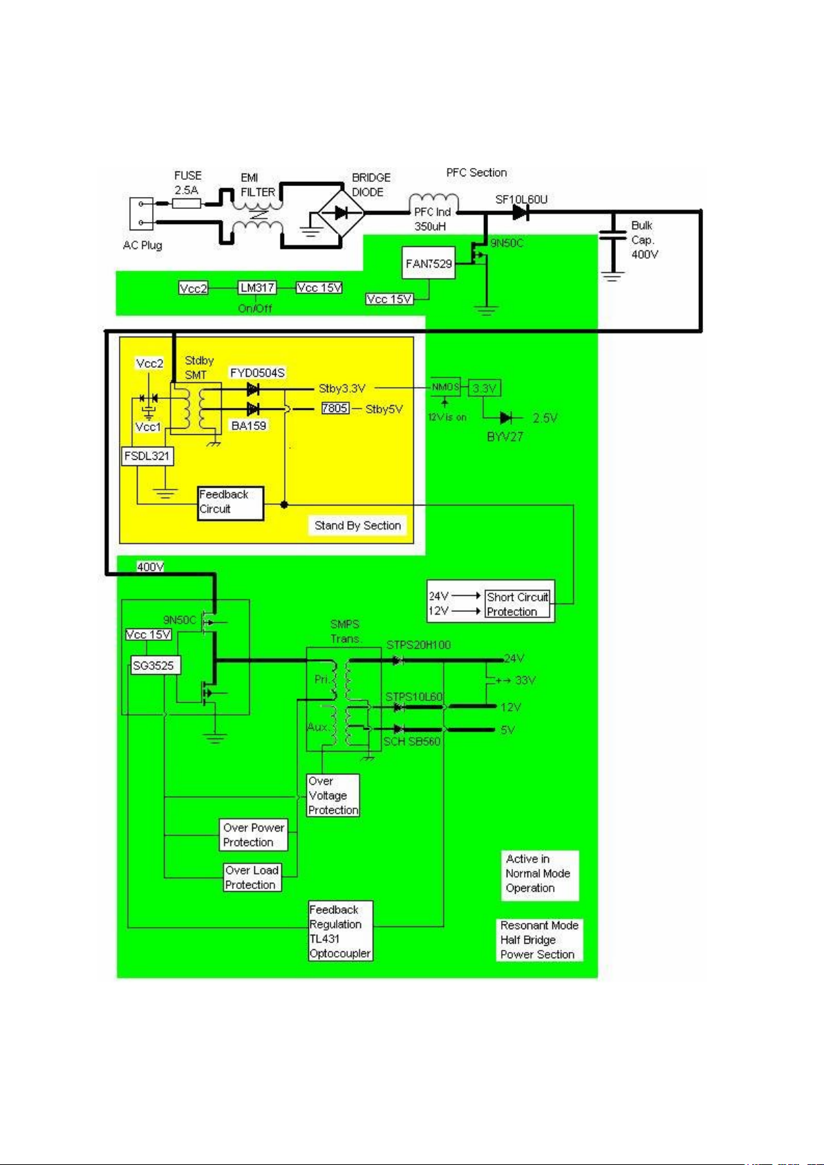
The DC voltages required at various parts of the chassis and inverter are provided by an
internal power supply unit
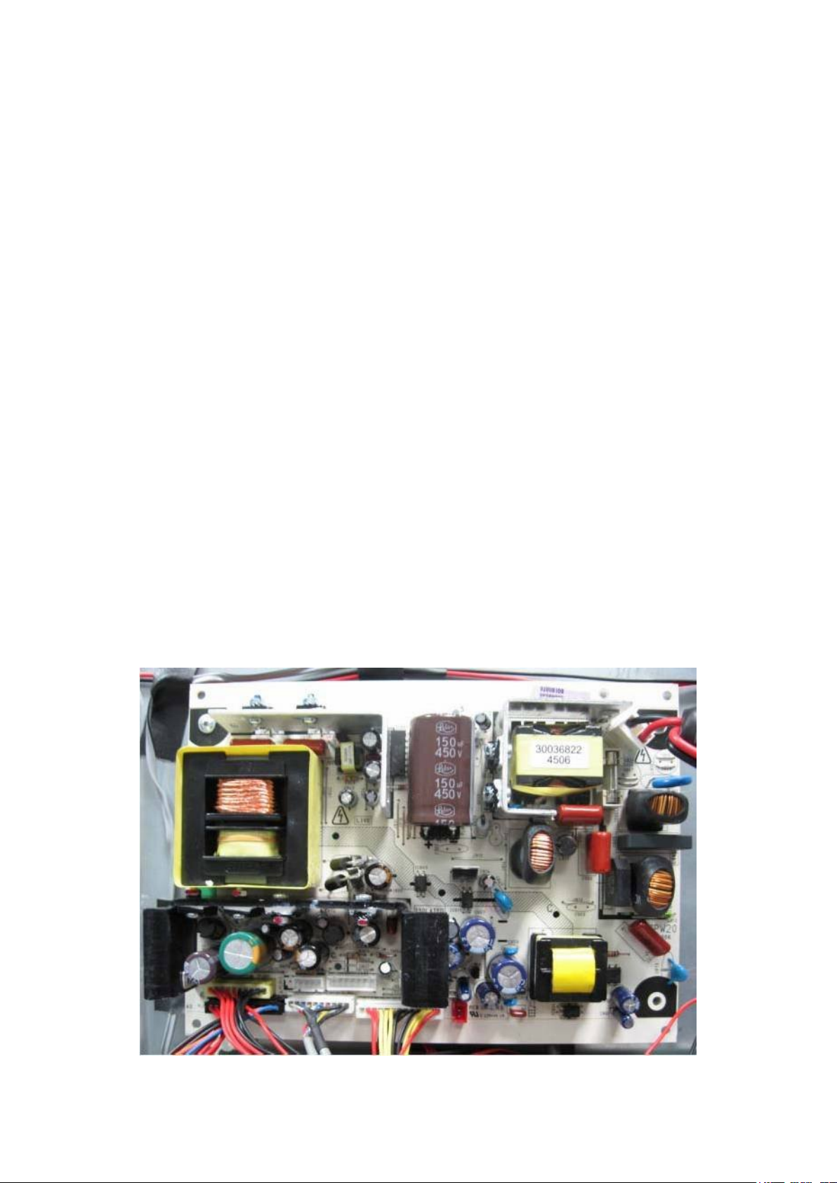
3.1. Board Description
17PW20 is a TFT-LCD power board designed by Vestel Power Electronics Design Group to
make a replacement with 17PW15-9 to obtain the stand-by power loss less than 1W. The
target sizes are the same with 17PW15-9 power board. 26”,32” and 37” TFT televisions is
going to be produced with 17PW20 power board. There are two types of voltage ranges. One
configuration is for the 90-270V Voltage range to run in South American countries. The other
configuration is for the 170-270V Voltage range for European, Asian and African countries.
The board can supply power up to 180W obtaining reliability rules.
The board has an active PFC circuit and the power factor of the board is between 0.95-0.99.
The PFC bulk voltage is set to 395V. The DC/DC converter circuit is a Resonant Mode Half
Bridge SMPS stage working around 65kHz switching frequency. The switching transformer
outputs are 24V, 12V and 5V. A 33V tuner voltage is obtained together with 24V and 12V
added in a capacitor and filtered with an 33V zener diode.
In the standby condition the Vcc voltages of the PFC IC and Half Bridge Power IC is cut off
and they don’t continue working. Stand-by circuit is another SMPS stage with a stand-by
transformer and a Flyback IC with internal mosfet. It works in a fixed 50kHz frequency. The
outputs of the Stand-by transformer is 3.3V and 8V. Stand by 5V is produced from 8V with a
LM7805 regulator.
The softswitch option from the on/off button is ready in this board. All of the outputs not only
the main power outputs and also the standby voltages can be cut off with a softswitch button.
3.2. Block Diagram
3.3 Input Specifications
3.3.1. Input Condition
Standart Voltage Range AC 220V-240V
Maximum Voltage
Range AC 170V-270V
Frequency Range 47Hz - 63Hz
3.3.2. Others
ITEM Specifications Test Conditions
Efficiency >89%
Inrush Current <160 A peak
Input Current <1.3 A Rms • AC 170V (Min Input Voltage)
0.4W
Standby Power
Consumption
1W
• AC 220V input Voltage •
At Full Load, Ta=25 oC
• AC 240V input Voltage •
Cold Start, Ta=25 oC
• AC 220V (Nom. input Voltage)
• No Load, Ta=25 oC
• AC 220V (Nom. Input Voltage)
• 3.3Vstby-75mA • 5Vstby-20mA, Ta=25 oC
• Other outputs have no load.
Max Input Power 210W
• AC 170V (Min Input Voltage) •
Outputs: 5V-2.5A, 3.3V-2A, 12V-2A, 33V-0.006A, 24V-6A
3.4. Output Specifications
3.4.1. Output Voltages & Load Conditions
CH #
CH1 3V3stby 3.35 3.3-3.4 +/- 5 0.03 0.5A
CH2 3V3 3.4 3.1-3.4 +/- 5 0.03 2A *1
CH3 2.5V 2.5 2.4-2.7 +/-5 0.03 2A *1
CH4 5Vstby 5.0 5.0-5.07 +/- 5 0.0 30mA
CH5 5V 5.0 4.63-5 +/- 5 0.03 2.5A
CH6 12V 11.6 11.5-12.2 +/- 5 0.03 2A
CH7 24V 23.85 23.4-24.3 +/- 3 0.03 6A
CH8 33V 34V 34-35 +/- 2 0.03 6mA
Output
Name
Output
Typical
(V)
Variable
Voltage Range
(V)
Voltage
Tolerance(%)
Output Current (A)
Min Max
*1. Total combination of 3V3stby, 3V3 and 2.5V can be max 2A
3.4.2. Ripple & Noise Figure
Ripple &Noise (Vp-p) *2
CH #
CH1 3V3stby 2mVp-p 20mVp-p 60mVp-p
CH2 3V3 5mVp-p 15mVp-p 130mVp-p
CH3 2.5V 5mVp-p 15mVp-p 130mVp-p
CH4 5Vstby 2mVp-p 15mVp-p 30mVp-p
CH5 5V 5mVp-p 60mVp-p 50mVp-p
CH6 12V 9mVp-p 60mVp-p 125mVp-p
CH7 24V 17mVp-p 85mVp-p 300mVp-p
CH8 33V 13mVp-p 50mVp-p 50mVp-p
Output
Name
All outputs at
min load
All outputs at
max load
250Hz %50%100 Load
Change*1
*1. Output current of specified voltage is changed from 50% to100% at 250Hz frequency
while all other outputs are at maximum load.
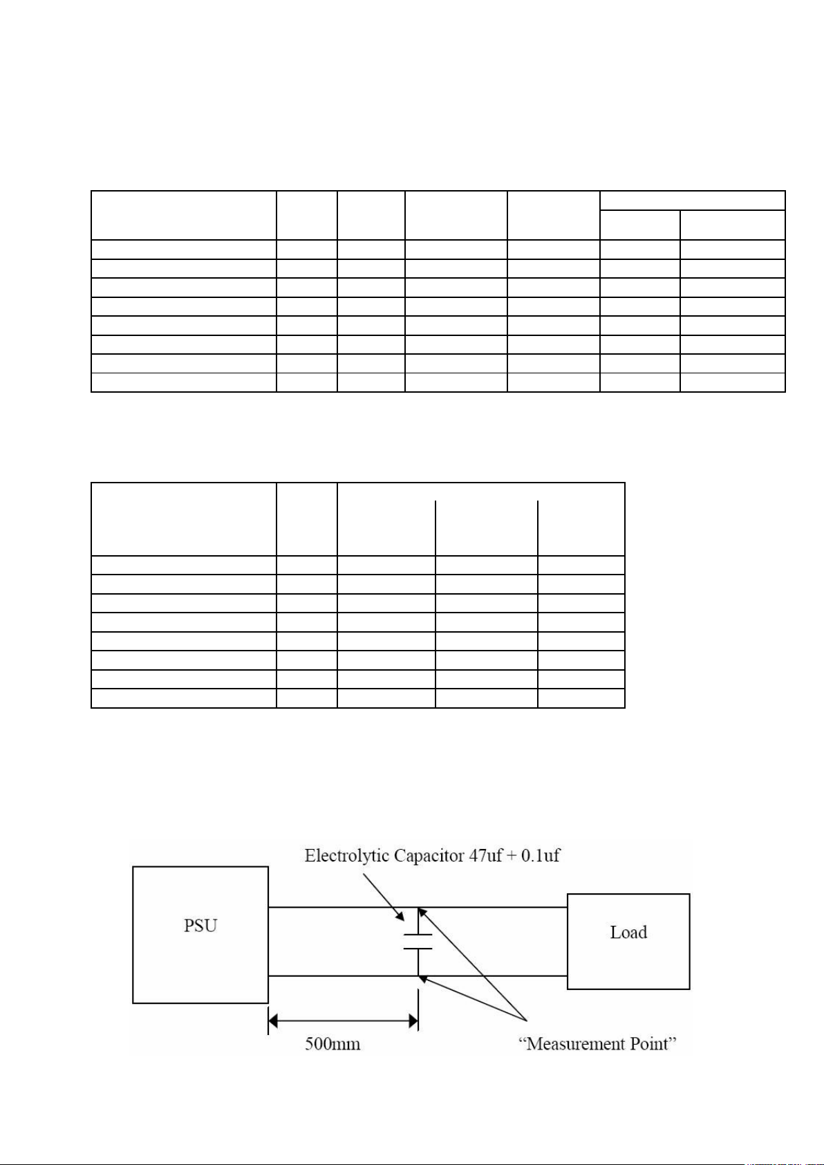
*2. Ripple & Noise Measurement Method
Measuring Device Part Number: Tektronix DPO7104 Digital Phosphor Oscilloscope 20Mhz
Bandwidth, AC mode
3.4.3. Output Protection
Circuit
Protection
No Safety
CH #
CH1 3V3stby 3.35 500mA Auto-Restart 5.8 V
CH2 3V3 3.4 6A* Auto-Restart 5.8 V
CH3 2.5V 2.5 *9 - - -
CH4 5Vstby 5.0 150mA Auto-Restart *6
CH5 5V 5.0 *3 *3 *4
CH6 12V 11.6 *3 *3 *5
CH7 24V 23.85 12A Auto-Restart 28V
CH8 33V 34V - *2 R878 *7
Output
Name
Output
Typical
(V)
*1 Over
Current
Protection
(A)
Current
Protection Mode
Over
Voltage
Protection
(V)
Over
Voltage
Protection
Mode
AutoRestart
AutoRestart
AutoRestart
AutoRestart
AutoRestart
AutoRestart
*1 The Over current protection point is measured by resistor load when other output load is at
maximum.
*2 No Over-Current Protection, current is limited by R878.
*3 No Over-Current Protection, Only short Circuit protection is available.
*4 No Over-Voltage Protection. Max. Voltage can be 5.6V.
*5 No Over Voltage Protection. Max. Voltage can be 15V.
*6 No Over Voltage Protection. Only can be 9V if 5V regulator is shorted.
*7 No Over Voltage Protection. Can be 46V if R878 shorted, and 33V zener is opened.
*8 Maximum stable current can be 2A. During a short circuit, current can reach max 6A peak
before protection.
*9 2.5V is related to 3V3 with a diode.
Short
Failure
3.5. Enviroment Condition
Operating Temperature 0°C - 40°C
3.6. Connector Pin Assigment
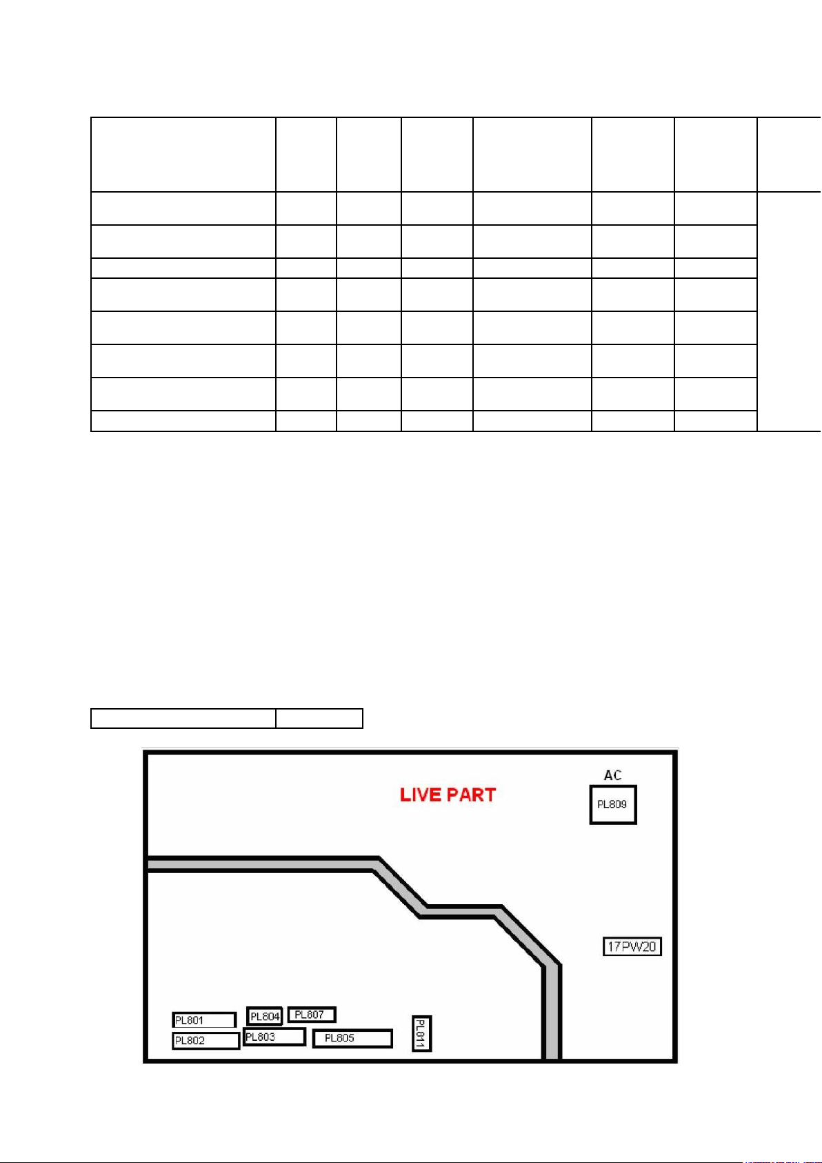
3.6.1. PL801 – OUTPUT
Model No: 10P 2.54MM TOP or equivalent (30037619)
PIN Signal Name
1 24V
2 24V
3 24V
4 24V
5 24V
6,7 GND
8,9 GND
10 GND
Description
Soundcard and Speaker Voltage
Soundcard and Speaker Voltage
Soundcard and Speaker Voltage
Soundcard and Speaker Voltage
Soundcard and Speaker Voltage
Secondary side ground
Secondary side ground
Secondary side ground
3.6.2. PL802 – OUTPUT (Connected to Inverter)
Model No: 12P 2.54MM TOP or equivalent (30029522)
PIN Signal Name
1 24V
2 24V
3 24V
4 24V
5 24V
6 GND
7 GND
8 GND
9 A/D DIM Select
10 D_DIM
11 A_DIM
12
BL_ON/OFF Backlight on/off signal from MainBoard
Description
Inverter Voltage
Inverter Voltage
Inverter Voltage
Inverter Voltage
Inverter Voltage
Secondary side ground
Secondary side ground
Secondary side ground
Control signal from MainBoard.
0V=analog dimming on
3.3V=digital dimming on
Digital Dimming Signal from MainBoard (PWM
signal)
Analog Dimming Voltage from
MainBoard (0-3.3V)(Bright-Dark)
3.6.3. PL803 – INPUT/OUTPUT
Model No: 10P 2.54MM TOP or equivalent (30032885)
PIN Signal Name
1 BL_ON/OFF
2 A_DIM
3 D_DIM
4 A/D_DIM_SEL
5 NC
6 ST_BY
7 33V
Description
Input. Backlight on/off signal from Mainboard(0-3.3V)
Input. Analog Dimming Voltage From
Mainboard (0-3.3V) (Bright-Dark)
Input. PWM Dimming signal from Mainboard
Input. Analog/Digital dimming selection from
Minboard
Not connected
Input. Stand by signal from Mainboard
>2V=stand by mode 0V=
open mode
Output. Tuner voltage.
8 12V
9 GND
10 GND
Output. 12V Vcc voltage
Secondary side Ground
Secondary side Ground
3.6.4. PL804 – OUTPUT
Model No: 4P 2.5MM TOP or equivalent (30033112)
PIN Signal Name
1 12V
2 12V
3 GND
4 GND
Description
IDTV card Voltage
IDTV card Voltage
GND
GND
3.6.5. PL805 – OUTPUT
Model No: 13P 2.54MM TOP or equivalent (30048878)
PIN Signal Name
1 +5V
2 +5V
3 +5V
4 VCC_3V3_ON
5 VCC_3V3_ON
6 VCC_3V3_ON
7 GND
8 GND
9 GND
10 GND
11 +3,3VSTBY 3.3V logic voltage in stand by mode
12
13
+3,3VSTBY 3.3V logic voltage in stand by mode
+5VSTBY 5V logic voltage in standby mode
Description
5V logic voltage in open mode for Mainboard
5V logic voltage in open mode for Mainboard
5V logic voltage in open mode for Mainboard
3.3V logic voltage in open mode
3.3V logic voltage in open mode
3.3V logic voltage in open mode
GND
GND
GND
GND
3.6.6. PL807 – OUTPUT
Model No: 7P 2.5MM TOP or equivalent (30037559)
PIN Signal Name
1 2.5V
2 33V
3 12V
4 GND
5 GND
6 5V
7 3.3V
Description
Optional IDTV Voltage
Tuner Voltage
12V Vcc voltage
Ground
Ground
5V logic
3.3V logic
6.7. PL811 – INPUT
Model No: 2P 2.5MM TOP or equivalent (30032632)
PIN Signal Name
1 GND
2 SW
Description
Ground
Soft-switch input

4. TUNER
The tuners used in the design are combined VHF, UHF tuners suitable for CCIR systems
B/G, H, L, L’, I/I’, and D/K. The tuning is available through the digitally controlled I2C bus
(PLL).
Description
The UV1316 tuner belongs to the UV 1300 family of tuners, which are designed to meet a
wide range of applications. It is a combined VHF, UHF tuner suitable for CCIR systems B/G,
H, L, L’, I and I’. The low IF output impedance has been designed for direct drive of a wide
variety of SAW filters with sufficient suppression of triple transient.
Features
1. Member of the UV1300 family small sized UHF/VHF tuners
2. Systems CCIR: B/G, H, L, L’, I and I’; OIRT: D/K
3. Digitally controlled (PLL) tuning via I2C-bus
4. Off-air channels, S-cable channels and Hyper band
5. Compact size
6. Complies to “CENELEC EN55020” and “EN55013”
Pin Configuration
1. Gain control voltage (AGC) : 4.0V, Max: 4.5V
2. Tuning voltage
3. I²C-bus address select : Max: 5.5V
4. I²C-bus serial clock : Min:-0.3V, Max: 5.5V
5. I²C-bus serial data : Min:-0.3V, Max: 5.5V
6. Not connected
7. PLL supply voltage : 5.0V, Min: 4.75V, Max: 5.5V
8. ADC input
9. Tuner supply voltage : 33V, Min: 30V, Max: 35V
10. Symmetrical IF output 1
11. Symmetrical IF output 2
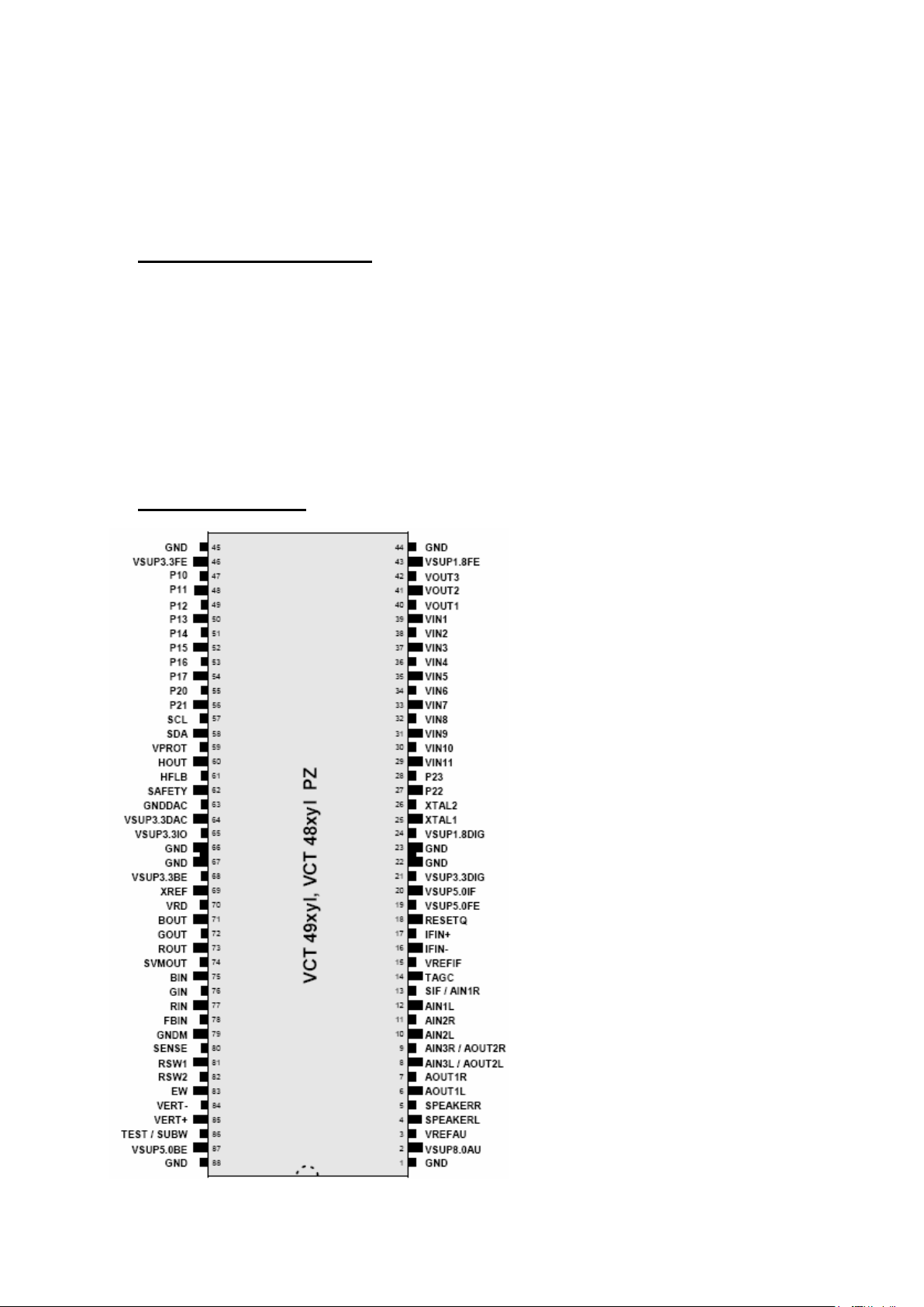
5. MICROCONTROLLER(VCTI)
General Features
The VCT 49xyI, VCT 48xyI is an IC family of high-quality single-chip TV processors.
Modular design and deep-submicron technology allow the economic integration of features in
all classes of single-scan TV sets. The VCT 49xyI, VCT 48xyI family is based on functional
blocks contained and approved in existing products like DRX 396xA, MSP 34x5G, VSP
94x7B, DDP 3315C, and SDA 55xx. Each member of the family contains the entire IF, audio,
video, display, and deflection processing for 4:3 and 16:9 50/60-Hz mono and stereo TV sets.
The integrated microcontroller is supported by a powerful OSD generator with integrated
Teletext & CC acquisition including on-chip page memory.
– Submicron CMOS technology
– Low-power standby mode

– Single 20.25 MHz reference crystal
– 8-bit 8051 instruction set compatible CPU
– Up to 256 kB on-chip program ROM
– WST, PDC, VPS, and WSS acquisition
– Up to 10 pages on-chip teletext memory
– Multi-standard QSS IF processing with single SAW
– FM Radio and RDS with standard TV tuner
– TV-sound demodulation:
• all A2 standards
• all NICAM standards
• BTSC/SAP with MNR (DBX optional)
• EIA-J
– Baseband sound processing for loudspeaker channel:
• volume and balance
• bass/treble or equalizer
• loudness and spatial effect (e.g. pseudo stereo)
• Micronas AROUND (virtual Dolby optional)
• Micronas BASS and Subwoofer output
• further optional and licence requiring sound enhancements as BBE, SRS Wow
– CVBS, S-VHS, YCbCr and RGB inputs
– ITU656 input
– 4H adaptive comb filter (PAL/NTSC)
– multi-standard color decoder (PAL/NTSC/SECAM)
– Macrovision Detection
– Nonlinear horizontal scaling “panorama vision”
– Luma and chroma transient improvement (LTI, CTI)
– Non-linear color space enhancement (NCE)
– Dynamic black level expander (BLE)
– Selective Color Enhancer (SCE)
– 8/10 bit ITU656 output
– Soft start/stop of H-drive
DRX Features
The DRX - Analog TV IF- Demodulator performs the entire multistandard Quasi Split
Sound (QSS) TV IF processing, AGC, video demodulation, and generation of the second
sound IF (SIF) requiring only one SAW filter. The alignment-free DRX does not need special
external components. All control functions and status registers are accessible via I2C bus
interface. Therefore, it simplifies the design of high-quality, highly standardized IF stages.
– Multistandard QSS IF processing with a single SAW
– Highly reduced amount of external components (no tank circuit, no potentiometers, no
SAW switching)
– Programmable IF frequency (38.9 MHz, 45.75 MHz, 32.9 MHz, 58.75 MHz, 36.125
MHz)
– Digital IF processing for the following standards:
B/G, D/K, I, L/L’, and M/N
– Standard specific digital post filtering
– Standard specific digital video/audio splitting
– Standard specific digital picture carrier recovery:
• alignment-free
• quartz-stable and accurate

• stable frequency lock at 100% modulation and overmodulation up to 150%
• quartz-accurate AFC information
– Programmable standard specific digital group delay equalization
– Automatically frequency-adjusted Nyquist slope, therefore optimal picture and sound
performance over complete lock in frequency range
– Standard-specific digital AGC and delayed tuner AGC with programmable tuner Take Over
Point
Multistandard Sound Processor (MSP) Features
The MSP receives the digital Sound IF signal from the DRX part. The MSP is able to
demodulate all TV sound standards worldwide including the digital NICAM system.
Depending on the VCTI version, the following demodulation modes can be performed. TV
stereo sound standards that are unavailable for a specific VCTI version are processed in
analog mono sound of the standard. In that case, stereo or bilingual processing will not be
possible.
– Sound demodulator and stereo decoder
– Audio processing for loudspeaker channels:
• volume
• Automatic Volume Correction (AVC)
• bass/treble or equalizer
• loudness
• balance
• configurable Subwoofer output
– Optional features for loudspeaker channels:
• Virtual Dolby Surround (VDS)
• SRS WOW
• BBE High Definition Sound
– PMQFP144-2 package:
• 6 analog audio inputs
• 4 analog audio outputs
– PSSDIP88-1 package:
• 4 analog audio inputs
• 2 analog audio outputs
• 2 configurable analog audio inputs/outputs
Video Features
The TVT is a Teletext decoder for decoding World System Teletext data, as well as Video
Programming System (VPS), Program Delivery Control (PDC), and Wide-Screen Signalling
(WSS) data used for PALplus transmissions (line 23). The device also supports Closed
Caption acquisition and decoding. The TVT provides an integrated general-purpose, fully
8051-compatible microcontroller with television-specific hardware features. The
microcontroller has been enhanced to provide powerful features such as memory banking,
data pointer, additional interrupts, etc. The on-chip display unit for displaying Level 1.5
Teletext data can also be used for customer-defined onscreen
displays.
The TVT has an internal XRAM of 20 KB and an internal ROM of up to 256 KB.
ROMless versions can address up to 1 MB of external RAM and ROM. The 8-bit
microcontroller runs at 296 ns cycle time. The controller with dedicated hardware does most
of the internal TTX acquisition processing, transfers data to/from external memory interface,
and receives/transmits data via I2C-bus interface. In combination with dedicated hardware,

the slicer stores TTX data in a VBI buffer of 1 KB. The microcontroller firmware performs all
the acquisition tasks (hamming and parity checks, page search, and evaluation of header
control bits) once per field. Additionally, the firmware can provide high-end Teletext features
like Packet-26 handling, FLOF/TOP and list-pages. The interface-to-user software is
optimized for minimal overhead. TVT is realized in deep submicron technology with 1.8 V
supply voltage and 3.3 V I/O (TTL compatible).
– 11 analog video inputs (CVBS/Y/C/RGB/YCbCr)
– 3 analog video outputs
– integrated Y+C adder
– integrated high-quality A/D converters and associated clamp and AGC circuits
– high-performance 4H comb filter (PAL/NTSC) with vertical peaking
– multistandard color decoder PAL/NTSC/SECAM including all substandards
– macrovision-compliant multistandard sync processing
– macrovision detection
– RGB/YCbCr component processing and associated contrast, color saturation and tint
circuits
– high-quality soft mixer controlled by fast blank (alpha blending)
– fast blank monitor via I2C
– ITU656 input
– linear horizontal scaling (0.25 to 4)
– nonlinear horizontal scaling “panorama vision”
– split screen (OSD and video side by side)
– letter box detector (auto-wide)
– noise measurement
Controller Features
The TVT is a Teletext decoder for decoding World System Teletext data, as well as Video
Programming System (VPS), Program Delivery Control (PDC), and Wide-Screen Signalling
(WSS) data used for PALplus transmissions (line 23). The device also supports Closed
Caption acquisition and decoding. The TVT provides an integrated general-purpose, fully
8051-compatible microcontroller with television-specific hardware features. The
microcontroller has been enhanced to provide powerful features such as memory banking,
data pointer, additional interrupts, etc.
– Single external 20.25 MHz crystal, all necessary clocks are generated internally
– Normal mode: 40.5 MHz CPU clock, Power Save mode: 10.125 MHz
– Up to 256 KB on-chip program ROM
– 256 byte on-chip program RAM
– 128 byte on-chip extended stack RAM
– 20 kilobyte on-chip extended data RAM (XRAM)
– Memory banking up to 1 MB
– Non-multiplexed 8-bit data and 20-bit address bus
– Eight 16-bit data pointer registers (DPTR)
– 4-level, 24-input interrupt controller
– Patch module for 16 ROM locations
– Two 16-bit reloadable timers
– Capture-compare timer for infrared decoding
– Watchdog timer
– UART
– Real time clock (RTC)
– PWM units (2 channels 14-bit, 6 channels 8-bit)
– 8-bit ADC (4 channels)
– I2C bus master/slave interface
– Up to 24 programmable I/O ports
– Flash version for PMQFP144 and PSSDIP88 packages (SST39LF020 or compatible)
– ROM-less version with 1 MB address space for external program and data memory
OSD & Teletext Features
The on-chip display unit for displaying Level 1.5 Teletext data can also be used for
customer-defined onscreen displays. The TVT has an internal XRAM of 20 KB and an
internal ROM of up to 256 KB. ROMless versions can address up to 1 MB of external RAM
and ROM.
In combination with dedicated hardware, the slicer stores TTX data in a VBI buffer of 1
KB. The microcontroller firmware performs all the acquisition tasks (hamming and parity
checks, page search, and evaluation of header control bits) once per field. Additionally, the
firmware can provide high-end Teletext features like Packet-26 handling, FLOF/TOP and listpages. The interface-to-user software is optimized for minimal overhead.
Pin Configuration
 Loading...