

Page 1

Page 2

TABLE OF CONTENTS
1. INTRODUCTION.......................................................................................................................5
2. TUNER........................................................................................................................................ 5
2.1 General description of UV1316:........................ ... ..... ..... ... ..... ... ..... ...... .. ...... .. ...... ..... ... ....5
2.2 Features of UV1316:..... .. ..................................................................................................5
2.3 Pinning: ........................................... ................................... ................................... ............ 6
3. AUDIO AMPLIFIER STAGE WITH MP7722................................................... .......................6
3.1 General Description................. ...... .. ...... ..... ... ..... ... ..... ..... ... ..... ... ..... ... ..... ...... .. ...... .. ...... ....6
3.2 Features ................................................................. .. ................................ ... .......................6
3.3 Applications ....................................................... ..... ...... .. ...... ..... ... ..... ..... ... ..... ...... .. .......... 7
3.4 Absolute Ratings..................... ...... .. ...... ..... ... ..... ..... ... ..... ...... .. ...... ..... ... ..... ..... ... ..... ... ....... 7
3.5 Pinning ............................................................ ................................... ...............................7
4. POWER STAGE.........................................................................................................................7
5. MICROCONTROLLER (VCTP) ...............................................................................................8
5.1 General Features.................................... ..... ..... ... ..... ... ..... ...... .. ...... ..... ... ..... ... ..... ..... ... .......8
5.2 Multistandard Sound Processor (MSP) Features ..............................................................9
5.3 Video Features......................... ... ..... ... ..... ...... .. ...... ..... ... ..... ... ..... ..... ... ..... ... ..... ...... .. .......... 9
5.4 Controller Features........................ .. ...... ..... ... ..... ... ..... ..... ... ..... ...... .. ...... ..... ... ..... ..... ... ... ..10
5.5 OSD & Teletext Features.............................................................. .. ...... ..... ... ..... ..... ... .....11
5.6 Port Allocation ........................................................................ ................................... . .... 11
6. DRX 3961A............................................................................................... ................................20
6.1 General Desription .................................. ...... .. ...... ..... ... ..... ..... ... ..... ...... .. ...... ..... ... ..... ... ..20
6.2 Features ................................................................. .. ................................ ... .....................20
7. SERIAL 64K I2C EEPROM M24C64WBN6..........................................................................21
7.1 General Description................. ...... .. ...... ..... ... ..... ... ..... ..... ... ..... ... ..... ... ..... ...... .. ...... .. ...... ..21
7.2 Features ................................................................. .. ................................ ... .....................21
7.3 Absolute Maximum Ratings.......................... ..... ..... ... ..... ...... .. ...... .. ...... ..... ... ..... ..... ... .....22
7.4 Pinning ............................................................ ................................... .............................22
8. CLASS AB STEREO HEADPHONE DRIVER TDA1308........................ ... ..........................22
8.1. General Description................... .....................................................................................22
8.2 Features ................................................................. .. ................................ ... .....................22
8.3. Pinning ........................................................................................................................... 23
9. SAW FILTER X6966M............................................................................................................ 23
9.1 Features:.......................................................... ... ................................ ... ..........................23
9.2 Pin configuration:............ ... .............................................................................................24
9.3 Frequency response:.............................................................. .. ................................... ..... 24
10. IC DESCRIPTIONS AND INTERNAL BLOCK DIAGRAM.............................................25
10.1. LM1117............................................................................................................................ 25
10.1.1. General Description.............. ................................................................ ... ..................25
10.1.2. Features.....................................................................................................................25
10.1.3. Applications .................................................................................... ..........................25
10.1.4. Absolute Maximum Ratings......................................................................................26
10.1.5. Pinning ...................................................................................................................... 26
10.2. LM1086............................................................................................................................ 26
10.2.1. General Description.............. ................................................................ ... ..................26
10.2.2. Features.....................................................................................................................26
10.2.3. Applications .................................................................................... ..........................26
10.2.4. Absolute Maximum Ratings......................................................................................27
10.2.5. Pinning ...................................................................................................................... 27
10.3. MP1593............................................................................................................................ 27
10.3.1. General Description.............. ................................................................ ... ..................2
7
Page 3

10.3.2. Features.....................................................................................................................28
10.3.3. Applications .................................................................................... ..........................28
10.3.4. Absolute Maximum Ratings......................................................................................28
10.3.5. Electrical Characteristics...........................................................................................29
10.3.6. Pinning ...................................................................................................................... 29
10.4. FDC642P..........................................................................................................................30
10.4.1. General Description............................. ... .................................. ................................30
10.4.2 . Features ............................................ ................................... .....................................30
10.4.3. Absolute Maximum Ratings......................................................................................30
10.4.4. Pinning ...................................................................................................................... 30
10.5. SIL9011............................................................................................................................31
10.5.1 Features .................................... .. ................................................................................31
10.6. 24LC02........... .................................. ................................... ................................... .......... 31
10.6.1. General Description.............. ................................................................ ... ..................31
10.6.2 Features .................................... .. ................................................................................31
10.6.3 Pinning ............................................................. .................................. ... .....................32
10.7. µPA672T..........................................................................................................................32
10.7.1. General Description.............. ................................................................ ... ..................32
10.7.2. Features.....................................................................................................................33
10.7.3 Absolute Maximum Ratings..................... ..... ..... ... ..... ... ..... ...... .. ...... ..... ... ..... ..... ... .....33
10.7.4 Pinning ............................................................. .................................. ... .....................33
10.8. M74HC4052..................................................................................................................... 33
10.8.1. General Description.............. ................................................................ ... ..................33
10.8.2. Features.....................................................................................................................33
10.8.3 Absolute Maximum Ratings..................... ..... ..... ... ..... ... ..... ...... .. ...... ..... ... ..... ..... ... .....34
10.8.4 Pinning ............................................................. .................................. ... .....................34
10.9. Max809.............................................................................................................................35
10.9.1. General Description.............. ................................................................ ... ..................35
10.9.2. Features.....................................................................................................................35
10.9.3 Absolute Maximum Ratings..................... ..... ..... ... ..... ... ..... ...... .. ...... ..... ... ..... ..... ... .....35
10.9.4 Pinning ............................................................. .................................. ... .....................36
10.10. 24LC21......................................................... .................................. ................................37
10.10.1. General Description................. ...... ..... ... ..... ... ..... ..... ... ..... ...... .. ...... .. ...... ..... ... ..... ... ..37
10.10.2. Features................................. ..................................................................................37
10.10.3 Absolute Maximum Ratings..................... ................................... .............................37
10.10.4 Pinning ..................................................................................................................... 38
11.SERVICE MENU SETTINGS.................................................................................................38
11.1. Video Setup........................................ .. ...... ..... ... ..... ... ..... ..... ... ..... ...... .. ...... ..... ... ..... ..... 38
11.2. AudioSetup........... ...... .. ...... ..... ... ..... ..... ... ..... ...... .. ...... ..... ..... ... ..... ...... .. ...... ..... ... ..... ..... 38
11.3. Options 1............................ ..... ... ..... ..... ... ..... ...... .. ...... ..... ... ..... ..... ... ..... ... ..... ...... .. ........ 39
11.4. Options 2............................ ..... ... ..... ..... ... ..... ...... .. ...... ..... ... ..... ..... ... ..... ... ..... ...... .. ........ 40
11.5. Service Scan/Tuning Setup.................................. ... .....................................................41
11.6. External Source Settings.............................. ................................................................41
11.7. Picture Mode................................................................................................................41
11.8. Reset TV-Set........................ ...... .. ...... ..... ... ..... ..... ... ..... ... ..... ...... .. ...... ..... ... ..... ..... ... ..... 42
12. SOFTWARE UPDATE DESCRIPTION.............................. .. ................................................ 42
2
12.1 Analog Software Update Vi a I
C...................................................................................... 42
12.2 Analog Software Update Via UART ................................................................................43
13. BLOCK DIAGRAMS................................... ..... ... ..... ..... ... ..... ... ..... ...... .. ...... ..... ... ..... ..... ... .....44
13.1. General Block Diagram............................... ... ..................................................................44
13.2. Power Management..........................................................................................................45
Page 4

13.3. DRX (IF Demodulator) Block Diagram........................................................................... 46
13.4. VCTP.............................................. .. ................................... ............................................. 47
13.4.1. General Block Diagram........................................................ ................................ ... ..47
13.4.2. MSP Block Diagram................................................................................................. 48
13.4.3 Video Processor of VCT 6wxyP Block Diagram................................................49
Page 5

1. INTRODUCTION
17MB22 Main Board consists of Micronas concept, VCTP as controller. This IC is
capable of handling Audio processing, video processing, motion adaptive
upconversion(MAU), Scaling-Display processing and FPD control (DPS),unified memory
for audio video and Text, 3D comb filter-PC connectivity , OSD and text processing.
TV supports PAL, SECAM, NTSC colour standards and multiple transmission standards
as B/G, D/K, I/I’, and L/L’ including German and NICAM stereo.
Sound system output is supplying 2x8W (10%THD) for stereo 8 speakers.
Supported peripherals are:
1 RF input VHF1, VHF3, UHF @ 75Ohm
1 FAV input
2 SCART sockets
1 SVHS input
1 Stereo Headphone input
1 YPbPr
1 PC input
1 HDMI input
1 Stereo audio input for PC
2. TUNER
As the thickness of the TV set has a limit, a horizontal mounted tuner is used in the
product, which is suitable for CCIR systems B/G, H, L/ L’, I/I’, and D/K. The tuning is
available through the digitally controlled I2C bus (PLL). Below you will find info on the
Tuner in use.
2.1 General description of UV1316:
The UV1316 tuner belongs to the UV 1300 family of tuners, which are designed to meet
a wide range of applications. It is a combined VHF, UHF tuner suitable for CCIR
systems B/G, H, L, L’, I and I’. The low IF output impedance has been designed for
direct drive of a wide variety of SAW filters with sufficient suppression of triple transient.
2.2 Features of UV1316:
• Member of the UV1300 family small sized UHF/VHF tuners
• Systems CCIR: B/G, H, L, L’, I and I’; OIRT: D/K
• Digitally controlled (PLL) tuning via I2C-bus
• Off-air channels, S-cable channels and Hyper band
• Compact size
• Complies with the requirements of radiation, signal handling capability and
immunity conforming to European standards “CENELEC EN55020” and
“EN55013”.
Page 6
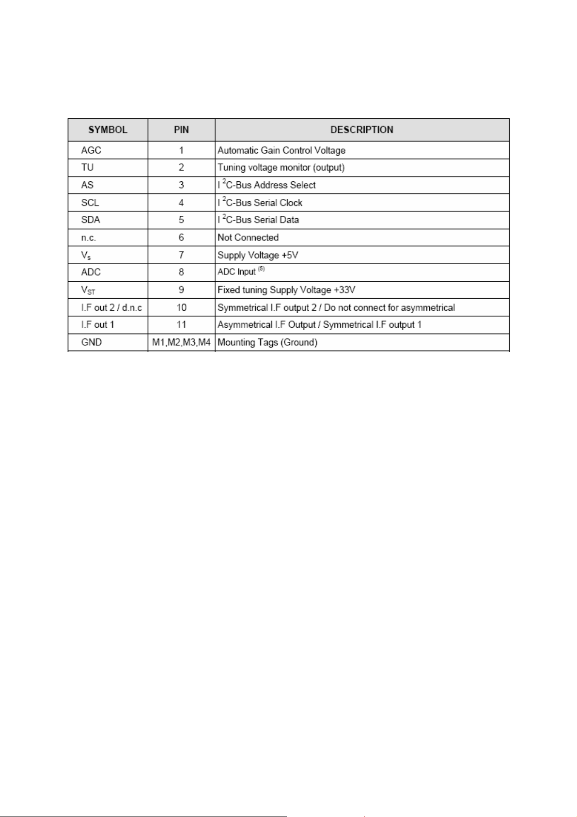
2.3 Pinning:
3. AUDIO AMPLIFIER STAGE WITH MP7722
3.1 General Description
The MP7722 is a stereo 20W Class D Audio amplifier, intended for use as low
frequency power amplifier in a wide range of applications in radio and TV sets.
It uses a minimum number of external components to complete a stereo Class D audio
amplifier.
3.2 Features
• 2 x 20W Output at VDD = 24V into a 4 load
• THD+N = 0.06% at 1W, 8
• 93% Efficiency at 20W
• Low Noise (190µV Typical)
• Switching Frequency Up to 1MHz
• 9.5V to 24V Operation from a Single Supply
• Integrated Startup and Shutdown Pop Elimination Circuit
• Thermal and Short Circuit Protection
• Integrated 180m Switches
• Mute/Standby Modes (Sleep)
• Thermally Enhanced 20-Pin TSSOP Package with Exposed Pad
Page 7
3.3 Application s
• Surround Sound DVD Systems
• Televisions
• Flat Panel Monitors
• Multimedia Computers
• Home Stereo Systems
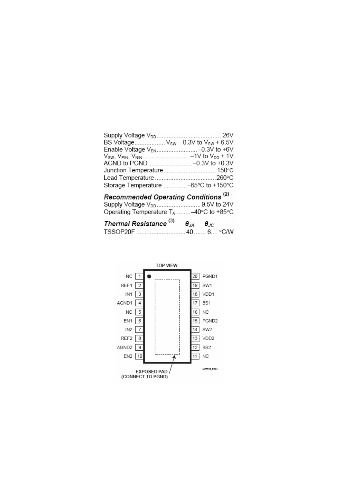
3.4 Absolute Ratings
3.5 Pinning
4. POWER STAGE
The DC voltages required at various parts of the chassis and inverters are provided by a
main power supply unit and power interface board. The main power supply unit is
designed for 24V and 12V DC supply. Power stage which is on-chasis generates +24V
for audio amplifier, 1.8V and 3.3V stand by voltage and 8V, 12V, 5V and 3.3V supplies
for other different parts of the chassis.
Page 8

5. MICROCONTROLLER (VCTP)
5.1 General Feat ures
The VCT 6wxyP is dedicated to high-quality FPD and double-scan TV sets. The VCT
6wxyP family is based on functional blocks contained and approved in existing products
like VCT 49xxI, VSP 94x5B, and DPS 94xxA.
Each member of the family contains the entire audio, video, up-conversion processing
for 4:3 and 16:9 50/
60 Hz progressive or 100/120 Hz interlaced stereo TV sets and the control/data
interface for flat-panel displays. The integrated microcontroller is supported by a
powerful OSD and graphics generator with integrated teletext acquisition.
Controller:
• High-performance 8-bit microcontroller, 8051 compatible
• Up to 512 kByte in system program Flash
• WST, PDC, VPS, and WSS acquisition
• Closed caption and V-chip acquisition
• Up to 10 page on chip teletext memory
• Up to 1000 pages with internal memory
• Up to 30 GPIO
Audio:
• Multistandard TV-sound demodulation:
-All A2/NICAM standards
-BTSC/SAP with DBX
-EIA-J
• Baseband sound processing for loudspeaker channel:
-Volume, bass, treble, loudness, balance
-Spatial effect (e.g. pseudo stereo)
-Micronas AROUND
(Virtual Dolby Surround optional)
-Micronas BASS
-BBE
-SRS WOW
-SRS TruSurround XT
-Lipsync function
Video:
• CVBS, S-VHS, YCrCb and RGB inputs
• HDTV YPrPb and RGB inputs
• ITU656 input
• Linedoubling with vertical detail enhancement (without internal memory)
• State of the art motion adaptive up conversion (with internal memory)
• 4H adaptive comb filter for PAL/NTSC (without internal memory)
• 3D comb filter for PAL/NTSC (with internal memory) (Optional)
• Internal SDR RAM interface
• Powerful horizontal and vertical scaling inclusive
• Nonlinear horizontal scaling “panorama vision”
• picture adaptive image improvements (DCE, LSE, CTI, SCE, NCE)
Page 9

• non-linear colorspace enhancement (NCE) with 32 programmable slopes and
sections per RGB component (blue stretch, static black stretch, gamma
correction).
• Dynamic contrast enhancement (DCE) (histogram based black stretch with peak
black and activity detection and contrast adaption)
• Luma sharpness enhancement (LSE)
• Color transient improvement (CTI)
• Selective color enhancement (SCE) for skin tone correction, blue and green
stretch
5.2 Multistandard Sound Processor (MSP) Features
The MSP receives the analog Sound IF signal from the tuner and converts it to digital
with its internal SIF-AD converter. The MSP is able to demodulate all TV sound
standards worldwide including the digital NICAM system. TV stereo sound standards
that are unavailable for a specific VCTP version are processed in analog mono sound of
the standard. In that case, stereo or bilingual processing will not be possible.
• Sound IF input
• Worldwide FM/AM-mono sound demodulation
• FM stereo sound demodulation (A2, EIA-J)
• BTSC/SAP demodulation with DBX
• NICAM demodulation
• FM radio & RDS/RBDS demodulation
• Automatic standard detection
• automatic volume correction (AVC)
• Automatic sound select
• Baseband processing for loudspeaker channel:
volume, bass, treble, loudness, balance
-spatial effect (e.g. pseudo stereo)
-Micronas AROUND
-Micronas BASS
-SRS WOW (optional)
-SRS TruSurround XT (optional)
-delayline for lipsync function (shared memory)
-Virtual Dolby Surround (optional)
• 1 I2S input for external ATSC/DVD decoder
• 1 I2S interface for audio delayline
• 1 SPDIF output
• Audio i/o switches
-4 analog stereo line inputs and 2 analog stereo line outputs (configurable 5
analog stereo line inputs and 1 analog stereo line output)
-1 analog stereo loudspeaker output
-1 analog subwoofer output
-1 analog stereo headphone output
5.3 Video Features
The TVT is a Teletext decoder for decoding World System Teletext data, as well as
Video Programming System (VPS), Program Delivery Control (PDC), and Wide-Screen
Signalling (WSS) data used for PALplus transmissions (line 23). The device also
supports Closed Caption acquisition and decoding.
Page 10

The TVT provides an integrated general-purpose, fully 8051-compatible microcontroller
with television-specific hardware features. The microcontroller has been enhanced to
provide powerful features such as memory banking, data pointer, additional interrupts,
shared memory access etc.
The TVT has an internal XRAM of 32 KB and a BOOT ROM of 4 KB. For operation the
code is fetched from a 16bit FLASH, which can be addressed up to 1 MByte.
The controller with dedicated hardware does most of the internal TTX acquisition
processing, transfers data to/from external memory interface, and receives/transmits
data via I2C-bus interface. In combination with dedicated hardware, the slicer stores
TTX data in a VBI buffer of 1 KB. The microcontroller firmware performs all the
acquisition tasks (hamming and parity checks, page search, and evaluation of header
control bits) once per field. Additionally, the firmware can provide high-end Teletext
features like Packet-26 handling, FLOF/TOP and list-pages. The interface-to-user
software is optimized for minimal overhead. TVT is realized in deep submicron
technology with 1.8 V supply voltage and 3.3 V I/O (TTL compatible).
• 16 analog video inputs (4xCVBS/Y/C + 3xRGB/YCrCb/YPrPb)
• Video input switch matrix
• 3 analog video outputs (integrated Y+C adder)
• 24-bit RGB/H/V/clk input (e.g. ext. DVI decoder) or 656 8bit input
• 656 8bit input/output (e. g. for external high-end up conversion by FRCA)
• Multi-standard color decoder PAL/NTSC/SECAM including all substandards
• 2D adaptive comb filter for PAL/NTSC with vertical peaking
• 3D-comb filter for PAL/NTSC (Optional)
• Macrovision compliant multi-standard sync processing
• Trilevel sync slicer for HDTV
• Macrovision detection
• High-quality soft mixer controlled by Fast Blank (alpha blending)
• Fastblank monitor via I2C
• Noise measurement
• Letterbox detection (auto-wide)
• Split screen (OSD and video side by side) and AV PIP
5.4 Controller F eat u res
The TVT is a Teletext decoder for decoding World System Teletext data, as well as
Video Programming System (VPS), Program Delivery Control (PDC), and Wide-Screen
Signalling (WSS) data used for PALplus transmissions (line 23). The device also
supports Closed Caption acquisition and decoding.
The TVT provides an integrated general-purpose, fully 8051-compatible microcontroller
with television-specific hardware features. The microcontroller has been enhanced to
provide powerful features such as memory banking, data pointer, additional interrupts,
shared memory access etc.
• High performance 8-bit microcontroller, 8051 instruction set compatible
• 81 MHz system clock, two machine cycles per instruction
• On-chip debug support (OCDS)
• Up to 512 kByte in system program Flash
• 256 byte on-chip program RAM
• 128 byte on-chip extended stack RAM
Page 11
• 4-level, 24-input interrupt controller
• Patch module for 16 ROM locations
• Two 16-bit reloadable timers
• Capture compare timer for infrared decoding
• Watchdog timer
• Uart
• Real time clock
• PWM units (2 channels 14-bit, 6 channels 8-bit)
• 8-bit ADC (4 channels)
• I2C bus master/slave interface
• Up to 32 programmable I/O ports
5.5 OSD & Teletext Features
The on-chip display unit for displaying Level 1.5 Teletext data can also be used for
customer-defined onscreen displays.
The TVT has an internal XRAM of 32 KB and a BOOT ROM of 4 KB. For operation the
code is fetched from a 16bit FLASH, which can be addressed up to 1 MByte.
In combination with dedicated hardware, the slicer stores TTX data in a VBI buffer of 1
KB. The microcontroller firmware performs all the acquisition tasks (hamming and parity
checks, page search, and evaluation of header control bits) once per field. Additionally,
the firmware can provide high-end Teletext features like Packet-26 handling, FLOF/TOP
and list-pages. The interface-to-user software is optimized for minimal overhead.
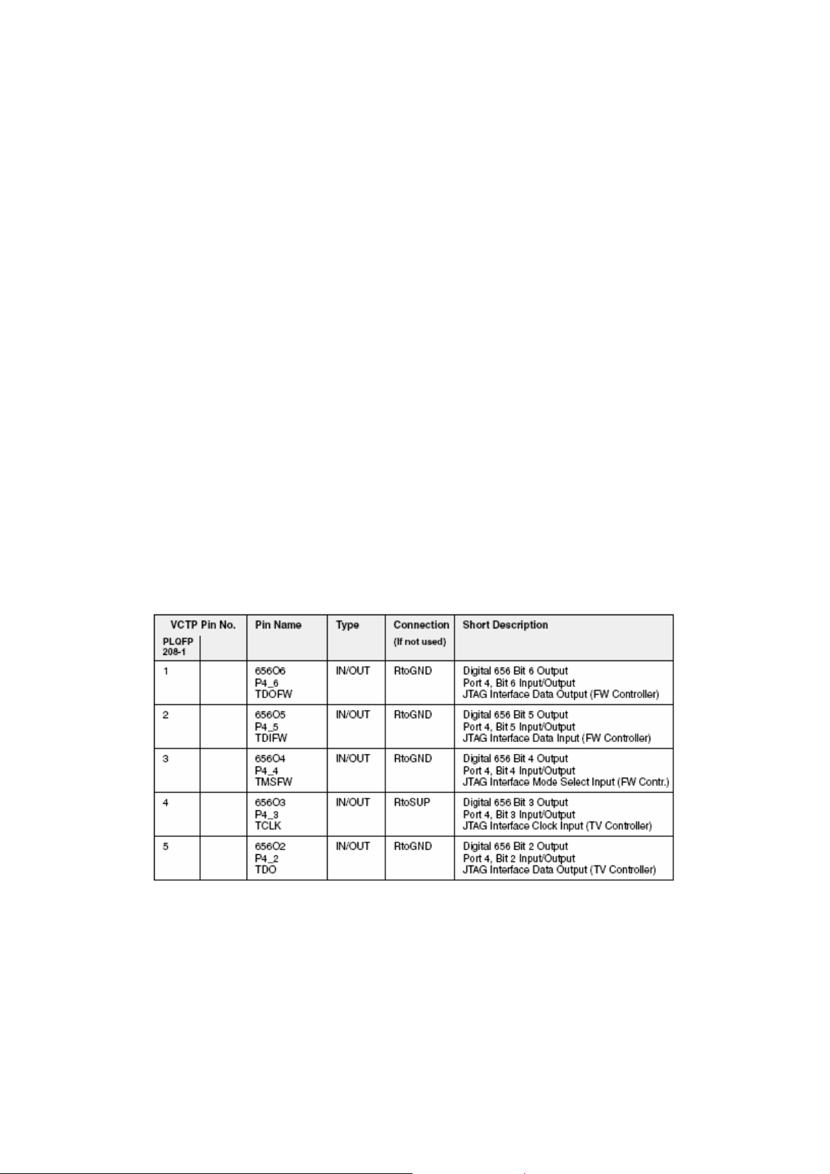
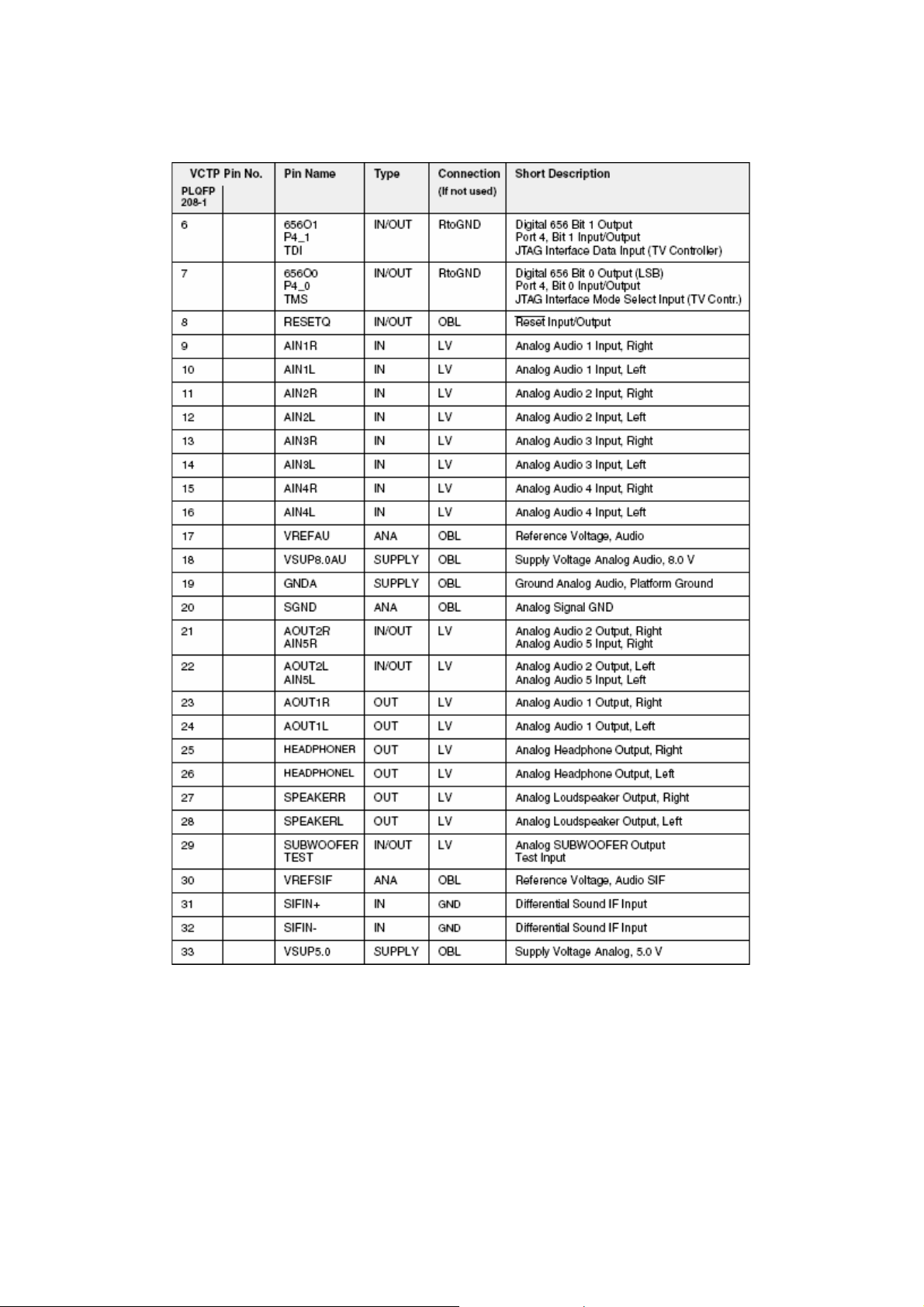
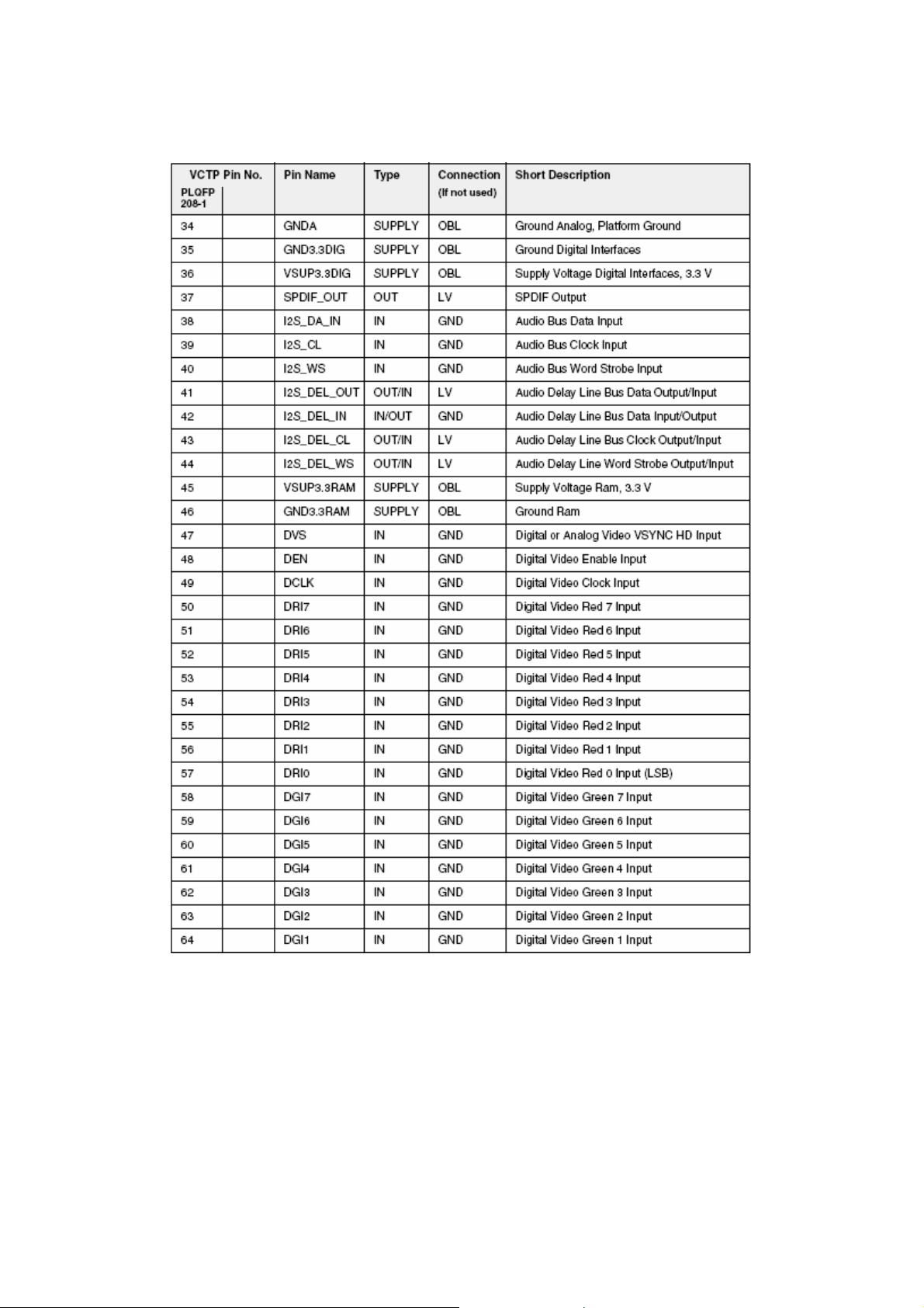
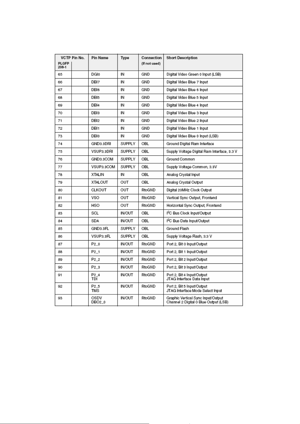
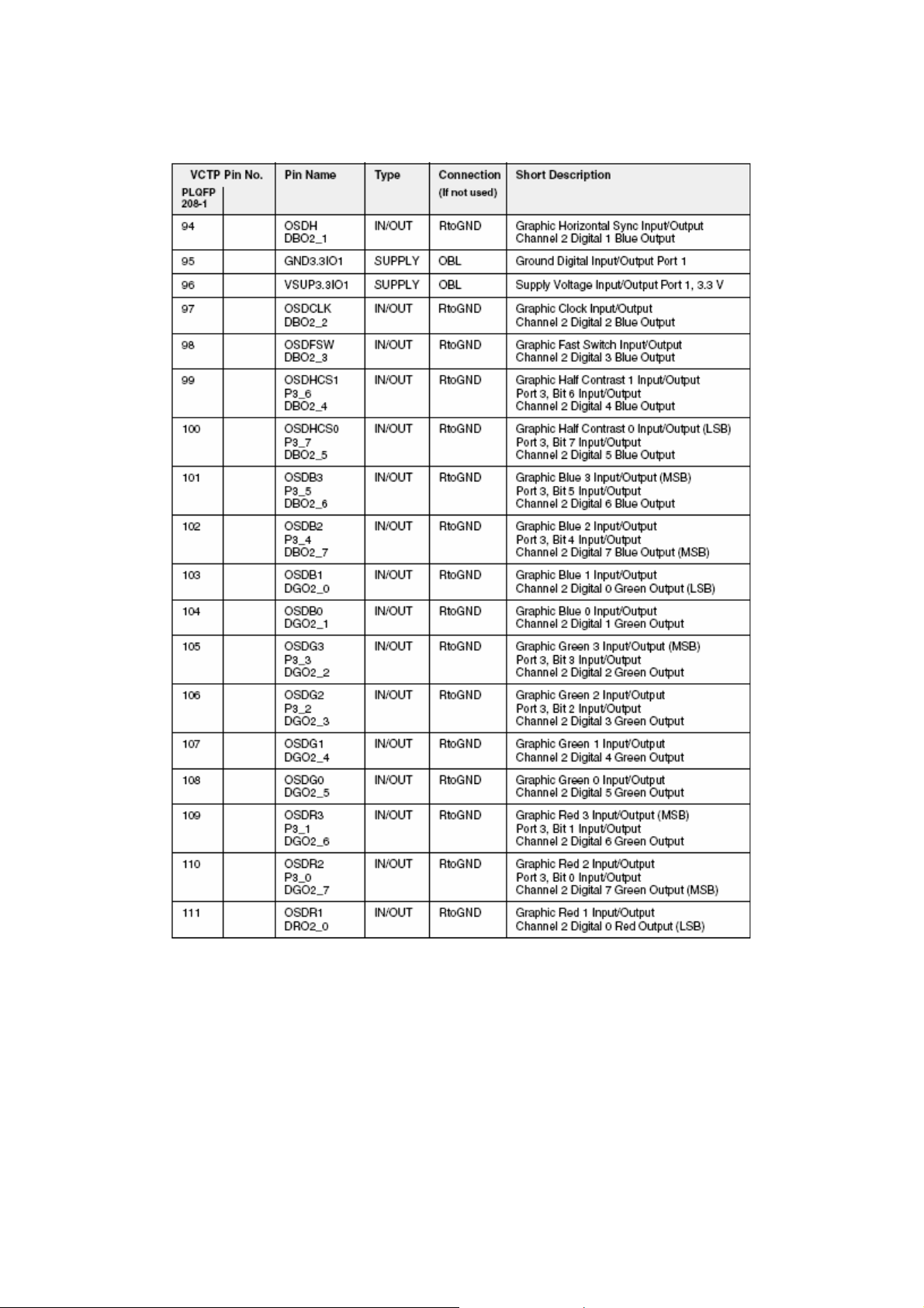
5.6 Port Allocati o n
Page 12
Page 13
Page 14
Page 15
Page 16

Page 17

Page 18

Page 19

Page 20

6. DRX 3961A
6.1 General Desription
The DSP-based Analog TV IF Demodulator DRX 396xA performs the entire
multistandard Quasi Split Sound (QSS) TV IF processing, AGC, video demodulation,
and generation of the sound IF (SIF), requiring only one SAW filter. The IC is designed
for applications in TV sets, VCRs, PC cards, and TV tuners.
The alignment-free DRX 396xA does not need special external components. All control
functions and status registers are accessible via I2C bus interface.
6.2 Features
• Multistandard QSS IF processing with a single SAW
• Highly reduced amount of external components (no tank circuit, no
potentiometers, no SAW switching)
Page 21

• Programmable IF frequency (38.9 MHz, 45.75 MHz, 32.9 MHz, 58.75 MHz,
36.125 MHz etc.)
• Digital IF processing for the following standards: B/G, D/K, I, L/L’, and M/N
• Standard specific digital post filtering
• Standard specific digital video/audio splitting
• Standard specific digital picture carrier recovery:
-Alignment-free
-Quartz-stable and accurate
-Stable frequency lock at 100% modulation and overmodulation up to
150%
-Quartz-accurate AFC information
• Programmable standard specific digital group delay equalization
• Automatically frequency-adjusted Nyquist slope, therefore optimum picture and
sound performance over complete lock in frequency range
• Standard-specific digital AGC and delayed tuner AGC with programmable tuner
take-over point
• Fast AGC due to linear structure
• Adaptive back porch control, therefore fast positive modulation AGC
• No sound traps needed at video output
• SIF output with standard-dependent pre-filtering and amplitude-controlled output
level
• Optimal sound SNR due to carrier recovery without quadrature distortions
• FM radio capability without external components and with standard TV tuner
• Prepared for digital TV (DVB-C, DVB-T, ATSC)
• I2C bus interface
7. SERIAL 64K I2C EEPROM M24C64WBN6
7.1 General Description
M24C64WBN6 is a 64 Kbit Electrically Erasable PROM. These I2C-compatible
electrically erasable programmable memory (EEPROM) devices are organized as
8192x8 bits. It supports 400kHz Protocol I2C uses a two-wire serial interface,
comprising a bi-directional data line and a clock line.
The M24C64WBN6 is available in the standard 8-pin (Vcc, WC, SDA (i2c data), SCL
(i2c clock), Vss,E0,E1,E2). WC pin is critcal pin. If WP is high, writing is not possible to
EEPROM. If WP is low, writing is possible to EEPROM.
7.2 Features
• Two-Wire I2C Serial Interface Supports 400kHz Protocol
• Single Supply Voltage:
– 4.5 to 5.5V for M24Cxx
– 2.5 to 5.5V for M24Cxx-W
– 1.8 to 5.5V for M24Cxx-R
• Write Control Input
• BYTE and PAGE WRITE (up to 32 Bytes)
Page 22

• RANDOM and SEQUENTIAL READ Modes
• Self-Timed Programming Cycle
• Automatic Address Incrementing
• Enhanced ESD/Latch-Up Protection
• More than 1 Million Erase/Write Cycles
• More than 40-Year Data Retention
7.3 Absolute Maximu m Rat ings
7.4 Pinning
8. CLASS AB STEREO HEADPHONE DRIVER TDA1308
8.1. General Description
The TDA1308 is an integrated class AB stereo headphone driver contained in an SO8
or a DIP8 plastic package. The device is fabricated in a 1 mm CMOS process and has
been primarily developed for portable digital audio applications. It gets its input from two
analog audio outputs (DACA_L and DACA_R) of MSP 34x0G. The gain of the output is
adjustable by the feedback resistor between the inputs and outputs.
8.2 Features
• Wide temperature range
• No switch ON/OFF clicks
• Excellent power supply ripple rejection
• Low power consumption
• Short-circuit resistant
• High performance
• High signal-to-noise ratio
Page 23

• High slew rate
• Low distortion
• Large output voltage swing.
• Power supply maximum 60 mW to 32 (THD<0.1%)
• 5V single supply
• SNR 110 dB
• Power supply ripple rejection
• Typically 3 mA supply current at no load
8.3. Pinning
9. SAW FILTER X6966M
9.1 Features:
- IF filter for digital cable TV
- Plastic package SIP5K
Page 24

9.2 Pin configuration:
1 Input
2 Input - ground
3 Chip carrier - ground
4 Output
5 Output
9.3 Frequency respon se:
Page 25

10. IC DESCRIPTIONS AND INTERNAL BLOCK DIAGRAM
LM1117
LM1086
MP1593
FDC642P
SIL9011
24LC02
µPA672T
M74HC4052
Max809
24LC21
10.1. LM1117
10.1.1. General Description
The LM1117 is a series of low dropout voltage regulators with a dropout of 1.2V at
800mA of load current. It has the same pin-out as National Semiconductor’s industry
standard LM317. The LM1117 is available in an adjustable version, which can set the
output voltage from 1.25V to 13.8V with only two external resistors. In addition, it is also
available in five fixed voltages, 1.8V, 2.5V, 2.85V, 3.3V, and 5V. The LM1117 offers
current limiting and thermal shutdown. Its circuit includes a zener trimmed bandgap
reference to as-sure output voltage accuracy to within ±1%. The LM1117 series is
available in SOT- 223, TO-220, and TO-252 D-PAK packages. A minimum of 10µF
tantalum capacitor is required at the output to improve the transient response and
stability.
10.1.2. Features
• Available in 1.8V, 2.5V, 2.85V, 3.3V, 5V, and Adjustable Versions
• Space Saving SOT-223 Package
• Current Limiting and Thermal Protection
• Output Current 800mA
• Line Regulation 0.2% (Max)
• Load Regulation 0.4% (Max)
• Temperature Range
• LM1117 0°C to 125°C
• LM1117I -40°C to 125°C
10.1.3. Applications
• 2.85V Model for SCSI-2 Active Termination
• Post Regulator for Switching DC/DC Converter
• High Efficiency Linear Regulators 15
• 32” TFT TV Service Manual 10/01/2005
• Battery Charger
• Battery Powered Instrumentation
Page 26

10.1.4. Absolute Maximum Ratings
10.1.5. Pinning
10.2. LM1086
10.2.1. General Description
The LM1086 is a low dropout three terminal regulator with 1.5A output current capability.
The output voltage is adjustable with the use of a resistor divider. Dropout is guarantee d
at a maximum of 500 mV at maximum output current. It's low dropout voltage and fast
transient response make it ideal for low voltage microprocessor applications. Internal
current and thermal limiting provides protection against any overload condition
that would create excessive junction temperature.
10.2.2. Features
• Low Dropout Voltage 500mV at 1.5A Output Current
• Fast Transient Response
• 0.015% Line Regulation
• 0.1% Load Regulation
• Current Limiting and Thermal Protecion.
• Adjustable or Fixed Output Voltage(1.8, 2.5, 2.85, 3.0, 3.3, 3.45, 5.0V)
• Surface Mount Package SOT-223 & TO-263 (D2 Package)
• 100% Thermal Limit Burn-in
10.2.3. Applications
• Battery Charger
Adjustable Power Supplies
•
Constant Current Regulators
•
•
Portable Instrumentation
High Efficiency Linear Power Supplies
•
Page 27

• High Efficiency "Green" Computer Systems
SMPS Post-Regulator
•
Power PC Supplies
•
• Powering VGA & Sound Card
10.2.4. Absolute Maximum Ratings
10.2.5. Pinning
10.3. MP1593
10.3.1. General Description
The MP1593 is a step-down regulator with an internal Power MOSFET. It achieves 3A
continuous output current over a wide input supply range with excellent load and line
regulation. Current mode operation provides fast transient response and eases loop
stabilization. Fault condition protection includes cycle-by-cycle current limiting and
thermal shutdown. Adjustable soft-start reduces the stress on the input source at turnon. In shutdown mode the regulator draws 20µA of supply current. The MP1593
requires a minimum number of readily available external components to complete a 3A
step down DC to DC converter solution.
Page 28

10.3.2. Features
• 3A Output Current
• Programmable Soft-Start
• 100m Internal Power MOSFET Switch
• Stable with Low ESR Output Ceramic Capacitors
• Up to 95% Efficiency
• 20µA Shutdown Mode
• Fixed 385KHz Frequency
• Thermal Shutdown
• Cycle-by-Cycle Over Current Protection
• Wide 4.75 to 28V Operating Input Range
• Output Adjustable from 1.22V
• Under Voltage Lockout
• Available in 8-Pin SOIC Package
10.3.3. Applications
• Distributed Power Systems
• Battery Chargers
• Pre-Regulator for Linear Regulators
• Flat Panel TVs
• Set-Top Boxes
• Cigarette Lighter Powered Devices
• DVD/PVR Devices
10.3.4. Absolute Maximum Ratings
Page 29

10.3.5. Electrical Characteristics
10.3.6. Pinning
Pin1:BS
High-Side Gate Drive Boost Input. BS supplies the drive for the high-side N-Channel
MOSFET switch. Connect a 10nF or greater capacitor from SW to BS to power the high
side switch.
Pin2:IN
Power Input. IN supplies the power to the IC, as well as the step-down converter
switches. Drive IN with a 4.75V to 28V power source. Bypass IN to GND with a suitably
large capacitor to eliminate noise on the input to the IC.
Pin3:SW
Power Switching Output. SW is the switching node that supplies power to the output.
Connect the output LC filter from SW to the output load. Note that a capacitor is required
from SW to BS to power the high-side switch
Pin4:GND
Ground.
Pin5:FB
Feedback Input. FB senses the output voltage to regulate that voltage. Drive FB with a
resistive voltage divider from the output voltage. The feedback threshold is 1.222V.
Pin6:COMP
Compensation Node. COMP is used to compensate the regulation control loop. Connect
a series RC network from COMP to GND to compensate the regulation control loop. In
some cases, an additional capacitor from COMP to GND is required.
Pin7:EN
Enable Input. EN is a digital input that turns the regulator on or off. Drive EN high to t urn
on the regulator, drive EN low to turn it off. An Under Voltage Lockout (UVLO) function
can be implemented by the addition of a resistor divider from VIN to GND. For complete
low current shutdown its needs to be less than 0.7V. For automatic startup, leave EN
unconnected.
Pin8:SS
.
Page 30

Soft-Start Control Input. SS controls the soft-start period. Connect a capacitor from SS
to GND to set the soft-start period. A 0.1µF c apacitor sets the soft-start period to 10ms.
To disable the soft-start feature, leave SS unconnected.
10.4. FDC642P
10.4.1. General Description
This p-channel 2.5V specified MOSFET is produced using Fairchild’s advanced
PowerTrench process that has been especially tailored to minimize on state resistance
and yet maintain low gate charge for superior switching performance.
10.4.2 . Features
10.4.3. Absolute Maximum Ratings
10.4.4. Pinning
Page 31

10.5. SIL9011
The Sil 9011 is a third generation HDMI re ceiver compatible with the HDMI 1.1 specific ation.
Backwards compatibility with DVI 1.0 allows HDMI systems to connect to existing DVI 1.0
hosts over a single cable.
The Sil 9011 is capable of receiving and outputting 2 to 8 channels of digital audio of up to
192kHz. An industry-standard I
S/PDIF port supports up to 96kHz audio.
Silicon Image’s HDMI receivers use the latest generation of PanelLink TMDS core technology.
These PanelLink cores pass all HDMI compliance tests.
10.5.1 Features
• HDMI 1.1, HDCP 1.1 and DVI 1.0 compliant receiver
• Integrated PanelLink core supports:
DTV resolutions (480i/576i/480p/576p/720p/1080i)
PC resolutions (VGA, SVGA, XGA, SXGA, UXGA) up to 165MHz.
• Digital video interface supports video processors:
24-bit and 48-bit RGB/ YCbCr 4:4:4
16/20/24-bit YCbCr 4:2:2
8/10/12-bit YCbCr 4:2:2 (ITU BT.656)
• S/PDIF output supports bothIEC 60958 and IEC 67937 for PCM, Dolby Digital,
DTS digital or any S/PDIF type audio transmission (32-96kHz Fs)
• Four Programmable I
• Sample rates up to 192kHz
• Auto audio error detection with programmable soft mute.
• Integrated HDCP decryption engine for receiving protected audio and video
content
• Pre-programmed HDCP keys provide highest level of key security, simplifies
manufacturing
2
S port allows direct connection to low-cost audio DACs. An
2
S outputs for connection to low-cost audio DACs.
10.6. 24LC02
10.6.1. General Description
24AA02/24LC02B (24XX02*) is a 2 Kbit Electrically Erasable PROM. The device is
organized as one block of 256 x 8-bit memory with a 2-wire serial interface. Low-voltage
design permits operation down to 1.8V, with standby and active currents of only 1µA
and 1mA, respectively. The 24XX02 also has a page write capability for up to 8 bytes of
data.
10.6.2 Features
• Single supply with operation down to 1.8V
• Low-power CMOS technology
-1mA active current typical
-1µA standby current typical (I-temp)
Page 32

• Organized as 1 block of 256 bytes (1 x 256 x 8)
2
• 2-wire serial interface bus, I
C™ compatible
• Schmitt Trigger inputs for noise suppression
• Output slope control to eliminate ground bounce
• 100 kHz (24AA02) and 400 kHz (24LC02B) compatibility
• Self-timed write cycle (including auto-erase)
• Page write buffer for up to 8 bytes
• 2ms typical write cycle time for page write
• Hardware write-protect for entire memory
• Can be operated as a serial ROM
• Factory programming (QTP) available
• ESD protection > 4,000V
• 1,000,000 erase/write cycles
• Data retention > 200 years
• 8-lead PDIP, SOIC, TSSOP and MSOP packages
• 5-lead SOT-23 package
• Pb-free finish available
• Available for extended temperature ranges:
-Industrial (I): -40°C to +85°C
-Automotive (E): -40°C to +125°C
10.6.3 Pinning
10.7. µPA672T
10.7.1. General Description
N-channel Mos-Fet array for switching.The µPA672T is a super-mini-mold device
provided with two MOS FET elements. It achieves high-density mounting and saves
mounting costs.
Page 33

10.7.2. Features
• Two MOS FET circuits in package the same size as SC-70
• Automatic mounting supported
10.7.3 Absolute Maximum Ratings
10.7.4 Pinning
10.8. M74HC4052
10.8.1. General Description
The M74HC4052 is a dual four-channel analog MULTIPLEXER/DEMULTIPLEXER
fabricated with silicon gate C2MOS technology and it is pin to pin compatible with the
equivalent metal gate CMOS4000B series. It contains 8 bidirectional and digitally
controlled analog switches.
10.8.2. Features
• LOW POWER DISSIPATION: ICC = 4mA(MAX.) at TA=25°C
• LOGIC LEVEL TRANSLATION TO ENABLE 5V LOGIC SIGNAL TO
COMMUNICATE
• WITH ±5V ANALOG SIGNAL
• LOW "ON" RESISTANCE:
Page 34

70W TYP. (VCC - VEE = 4.5V)
50W TYP. (VCC - VEE = 9V)
• WIDE ANALOG INPUT VOLTAGE RANGE: ±6V
• FAST SWITCHING:
tpd = 15ns (TYP.) at TA = 25 °C
• LOW CROSSTALK BETWEEN SWITCHES
• HIGH ON/OFF OUTPUT VOLTAGE RATIO
• WIDE OPERATING SUPPLY VOLTAGE RANGE (VCC - VEE) = 2V TO 12V
• LOW SINE WAVE DISTORTION: 0.02% at VCC - VEE = 9V
• HIGH NOISE IMMUNITY: VNIH = VNIL = 28 % VCC (MIN.)
• PIN AND FUNCTION COMPATIBLE WITH 74 SERIES 4052
10.8.3 Absolute Maximum Ratings
10.8.4 Pinning
VEE supply pin is provided for analog input signals. It has an inhibit (INH) input terminal
to disable all the switches when high. For operation as a digital
multiplexer/demultiplexer, VEE is connected to GND.
A and B control inputs select one channel out of four in each section. All inputs are
equipped with protection circuits against static discharge and transient excess voltage.
Page 35

10.9. Max809
10.9.1. General Description
The MAX809 and MAX810 are costeffective system supervisor circuits designed to
monitor VCC in digital systems and provide a reset signal to the host processor when
necessary. No external components are required.
The reset output is driven active within 10 _sec of VCC falling through the reset voltage
threshold. Reset is aintained active for a timeout period which is trimmed by the factory
after VCC rises above the reset threshold. The MAX810 has an activehigh RESET
output while the MAX809 has an activelow RESET output. Both devices are available
in SOT23 and SC70 packages.
10.9.2. Features
• Precision VCC Monitor for 1.5 V, 1.8 V, 2.5 V, 3.0 V, 3.3 V, and 5.0 V Supplies
• Precision Monitoring Voltages from 1.2 V to 4.9 V Available in 100 mV Steps
• Four Guaranteed Minimum PowerOn Reset Pulse Width Available (1 ms, 20
ms, 100 ms, and 140 ms)
• RESET Output Guaranteed to VCC = 1.0 V.
• Low Supply Current
• Compatible with Hot Plug Applications
• VCC Transient Immunity
• No External Components
• Wide Operating Temperature: 40°C to 105°C
• PbFree Packages are Available
10.9.3 Absolute Maximum Ratings
Page 36

10.9.4 Pinning
Page 37

10.10. 24LC21
10.10.1. General Description
The 24LC21 is a 1K bit electrically erasable programmable memory (EEPROM), organized by 8
bits.This device can operate in two modes: Transmit Only mode and I2C bidirectional mode.
When powered, the device is in Transmit Only mode with EEPROM data clocked out from the
rising edge of the signal applied on VCLK.
10.10.2. Features
• 1 MILLION ERASE/WRITE CYCLES
• 40 YEARS DATA RETENTION
• 2.5V to 5.5V SINGLE SUPPLY VOLTAGE
• 400k Hz COMPATIBILITY OVER the FULL RANGE of SUPPLY VOLTAGE
• TWO WIRE SERIAL INTERFACE I2C BUS COMPATIBLE
• PAGE WRITE (up to 8 BYTES)
• BYTE, RANDOM and SEQUENTIAL READ MODES
• SELF TIMED PROGRAMMING CYCLE
• AUTOMATIC ADDRESS INCREMENTING
• ENHANCED ESD/LATCH UP PERFORMANCES
10.10.3 Absolute Maximum Ratings
Page 38

10.10.4 Pinning
11.SERVICE MENU SETTINGS
In order to reach service menu,
• First Press “MENU”
• Then press the remote control code, which is “4725”
11.1. Video Setup
• Panel Select <..................................>
CHI MEI 16/9 32 inch
LG 16/9 26 inch
SAMSUNG 16/9 32 inch
• Picture Mute <.....>
If “Yes” selected, “Picture mute” feature is active.
• Blue Screen <.....>
If “Yes” selected, “Blue Background” item is seen in “Feature”
menu.
• YC Delay <...........>
Tuner PAL <.....> Value between -8 to+7
Ext PAL <.....> Value between -8 to+7
SECAM <.....> Value between -8 to+7
NTSC <.....> Value between -8 to+7
• AGC (dB) <.....> Value between 0 to+8
11.2. AudioSetup
• Equalizer <.....>
If “Yes” selected, “Equalizer” item is seen in “Sound” menu.
Page 39

• BBE
• SRS WOW
• Virtual Dolby Surround <.....>
If “Yes” selected, Virtual Dolby Surround feature is seen in “Sound”
menu with selected Virtual Dolby Text.
• Virtual Dolby Text The selected item is seen as Virtual Dolby Srround Text.
3DS
Virtual Dolby
3D Panorama
• AVL <.....>
If “Yes” selected, “AVL” item is seen in “Sound” menu.
• Carrier Mute <.....>
If “Yes” selected, “Carrier mute” feature is active.
• Audio Delay Offset
• Prescale
FM Presc. AVL On <.......> Value between 0 to +127
AM Presc. AVL On <.......> Value between 0 to +127
NICAM Presc. AVL On <.......> Value between 0 to +127
I2S Presc. AVL On <.......> Value between 0 to +127
SCART Presc. AVL On <.......> Value between 0 to +127
FM Presc. AVL Off <.......> Value between 0 to +127
AM Presc. AVL Off <.......> Value between 0 to +127
NICAM Presc. AVL Off <.......> Value between 0 to +127
I2S Presc. AVL Off <.......> Value between 0 to +127
SCART Presc. AVL Off <.......> Value between 0 to +127
• Dynamic Bass <.....>
If “Yes” selected, “Dynamic Bass ” item is seen in “Sound” menu.
• Subwoofer <.....>
If “Yes” selected, “Subwoofer” item is seen in “Sound” menu.
11.3. Options 1
• VCTP Version <.......>
Basic+
Basic
• Double Digit <.....>
If “Yes” selected, “Double Digit” button is active for channel
selection.
• TEA6415C Available <.....>
If “Yes” selected, video switch IC is active on hardware.
• TEA642X Available<.....>
If “Yes” selected, audio switch IC is active on hardware.
• Power-Up Mode <.......>
StandBy If selected, TV opens in stand by mode.
L.State If selected, TV opens in Last State mode.
• TV Open Mode <.......>
Source
1st TV
Last TV
Page 40

• Select Languages <.......> “Yes” selected languages are seen as option under
the “Language” item in “Feature” menu
Language Set 1
o German <.......>
o French <.......>
o Spanish <.......>
o Italian <.......>
o Danish <.......>
o Finnish <.......>
o Swedish <.......>
Language Set 2
o Greek <.......>
o Norwegian <.......>
o Dutch <.......>
o Portuguse <.......>
o Polish <.......>
o Turkish <.......>
o Russian <.......>
o Czech <.......>
Language Set 3
o Hungarian <.......>
o Slovak <.......>
o Slovenian <.......>
o Romanian <.......>
o Bulgarian <.......>
o Croatian <.......>
o Serbian <.......>
o Hebrew <.......>
• First APS <.......>
If “Yes” selected, first time TV opens by asking APS.
• APS Volume <.......> value between 0 to+63
Burn In Mode <.......>
•
If “Yes” selected, TV opens with Burn-In mode. This mode is
used in manufacturing.
• APS Test
• HDMI WP <.......>
If “Yes” selected, HDMI EDID ROM is write protected.
11.4. Options 2
• Autostore <.......>
If “Yes” selected, Channel is automatically stored.
• Led Type <.............................>
1 Led 1 Colour
1 Led 2 Colours
2 Led 2 Colours
• PC PIP <.......>
• PC Stand By <.......>
Page 41

11.5. Service Scan/Tuning Setup
• Search for L/L’ <.......>
• Pref. Search Standard <...........>
BG, DK, I
L/L’
M
• Station Ident <.......>
• ATS Delay Time (ms) <.......> Value between 20 to 250
• Color Killer Threshold <... ....> Value between 0 to +255
• Tuner Options <.......>
Control Byte <.......> Value between 0 to +255
Low-Mid – Low Byte <.......> Value between 0 to +255
Low-Mid – High Byte <.......> Value between 0 to +255
Mid-High – Low Byte <.......> Value between 0 to +255
Mid-High – High Byte <.......> Value between 0 to +255
BSW1 <.......> Value between 0 to +255
BSW2 <.......> Value between 0 to +255
BSW3 <.......> Value between 0 to +255
11.6. External Source Settings
• DTV <.......>
• DVD <.......>
• Ext 2 S-Video <.......>
• Ext 3 <.......>
• Ext 3 S-Video <.......>
• FAV <.......>
• BAV <.......>
• S-Video <.......>
• HDMI 1 <.......>
• HDMI 2 <.......>
• YPbPr <.......>
• PC <.......>
11.7. Picture Mode
• Sources <.......>
Tuner
CVBS
RGB
SVHS
HDMI
YPbPr
PC
PIP
• Picture Mode <.......>
Dynamic
Natural
Cinema
Page 42

• Colour Temp <.......>
Cool
Normal
Warm
• Contrast <.......> Value between 0 to +63
• Brightness <.......> Value between 0 to +63
• Sharpness <.......> Value between 0 to +15
• Colour <.......> Value between 0 to +63
• Backlight <.......> Value between 0 to +255
• R <.......> Value between -63 to +63
• G <.......> Value between -63 to +63
• B <.......> Value between -63 to +63
11.8. Reset TV-Set
• Initialize NVM from ROM
Press green button to reset the NVM from ROM
12. SOFTWARE UPDATE DESCRIPTION
12.1 Analog Software Update Via I2C
Step.1
Short the second and third pins of PL_406. Power ON and keep shorting the pins 3-5
seconds.
Step.2
Then connect the I
Step.3
Connect the other end of the tool to PL_406.
Step.4
Run Cosima_VCTP Visual I
Step.5
When you click to box near “0” at “Bootloader Version” item, you will see “40”.
If you couldn’t see “40” or a “No Acknowledge from Slave!” is appeared,
There may be a connection problem sourced from PC port, or update tool.
Or you may forget to power ON.
Step.6
After “40” is seen, Click “Erase Flash”
Step.7
Select the bin. file from near the “Load Bin”
Step.8
Click “Load Bin” and load the required bin. file.
Step.9
2
Unpick the I
C cable from Chasis
2
C update tool to parallel port of PC.
2
C software update program.
Page 43

Step.10
Power off and on again TV set to produce hard reset.
Step.11
Initialize the NVM from “Reset TV-set” item from service menu
12.2 Analog Software Update Via UART
Step.1
Connect the serial cable from PC Com port to PL104 connector on 17PRG01 module
card.
Step.2
Connect the programming cable from PL 102 connector on 17PRG01 module card to
PL408 connector on TV chassis side. The arrow sign “” on the connector must see the
PCB side of the chassis. If TV is seen from the back cover, arrow sign must see the TVs
back cover
Step.3
Run a RS232 terminal tool like Hyper Terminal.
Step.4
Following settings of the terminal tool are necessary:
Protocol: Xmodem
Port: COMx
Baud Rate: 115200
Data Bits: 8
Parity: none
Stop Bits: 1
Com. Control: none
Step.5
Load the bin file from “Browse” and Click “Send”
Step.6
Power off and on again TV set to produce hard reset.
Page 44

13. BLOCK DIAGRAMS
13.1. General Block Diagram
Page 45

13.2. Power Management
Page 46

13.3. DRX (IF Demodulator) Block Diagram
Page 47

13.4. VCTP
13.4.1. General Block Diagram
Page 48

13.4.2. MSP Block Diagram
Page 49

13.4.3 Video Processor of VCT 6wxyP Block Diagram
 Loading...