

Vestel 17MB18P-3 23 Schematic

TABLE OF CONTENTS
1.
INTRODUCTION ......................................................................................................................................1
2. TUNER......................................................................................................................................................1
3. IF PART (TDA9886) .................................................................................................................................1
4. MULTI STANDARD SOUND PROCESSOR............................................................................................ 2
5. VIDEO SWITCH TEA6415 ....................................................................................................................... 2
6. AUDIO AMPLIFIER STAGE WITH TPA3002D2 ...................................................................................... 2
7. POWER .................................................................................................................................................... 2
8. MICROCONTROLLER SDA55XX............................................................................................................3
8.1. General Features............................................................................................................................... 3
8.2. External Crystal and Programmable Clock Speed............................................................................ 3
8.3. Microcontroller Features.................................................................................................................... 3
8.4. Memory.............................................................................................................................................. 3
8.5. Display Features................................................................................................................................ 3
8.6. ROM Characters................................................................................................................................ 3
8.7. Acquisition Features .......................................................................................................................... 4
8.8. Ports .................................................................................................................................................. 4
9. SERIAL ACCESS CMOS 16K (2048*8) EEPROM ST24C16.................................................................. 4
10. CLASS AB STEREO HEADPHONE DRIVER TDA1308 .........................................................................4
11. SAW FILTERS..........................................................................................................................................4
12. IC DESCRIPTIONS AND INTERNAL BLOCK DIAGRAM .......................................................................5
12.1. LM1117.............................................................................................................................................. 5
12.1.1. General Description................................................................................................................. 5
12.1.2. Features .................................................................................................................................... 5
12.1.3. Applications.............................................................................................................................. 5
12.1.4. Connection Diagrams.............................................................................................................. 5
12.2. LM2576.............................................................................................................................................. 6
12.2.1. General Description................................................................................................................. 6
12.2.2. Features .................................................................................................................................... 6
12.2.3. Pin description ......................................................................................................................... 6
12.3. LM317T .............................................................................................................................................7
12.3.1. Description................................................................................................................................7
12.3.2. Features .................................................................................................................................... 7
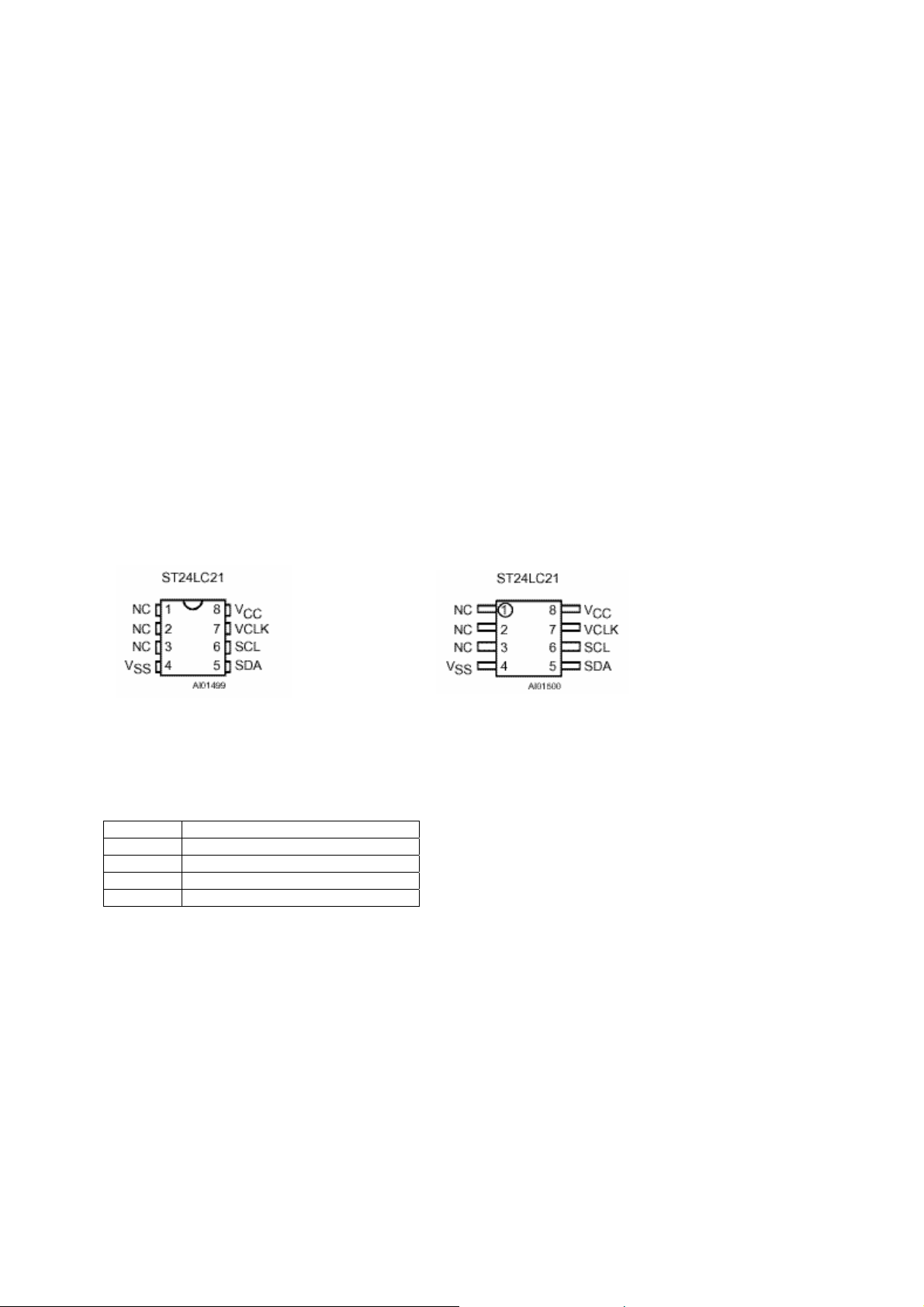
12.4. ST24LC21 .........................................................................................................................................8
12.4.1. Description................................................................................................................................8
12.4.2. Features .................................................................................................................................... 8
12.4.3. Pin connections........................................................................................................................ 8
12.5. TEA5114A .........................................................................................................................................9
12.5.1. General description ................................................................................................................. 9
12.5.2. Features .................................................................................................................................... 9
12.5.3. Pin Connections.......................................................................................................................9
12.6. TEA6415.......................................................................................................................................... 10
12.6.1. General description ............................................................................................................... 10
12.6.2. Features .................................................................................................................................. 10
12.6.3. Pinning....................................................................................................................................10
12.7. VPC3230D....................................................................................................................................... 11
12.7.1. General Description............................................................................................................... 11
12.7.2. Pin Connections and Short Descriptions............................................................................ 11
12.8. SDA55XX (SDA5550)......................................................................................................................13
12.8.1. General description ............................................................................................................... 13
12.9. TPA3003D2 ..................................................................................................................................... 14
12.9.1. General Description............................................................................................................... 14
12.9.2. Features .................................................................................................................................. 14
12.9.3. Pin Connection.......................................................................................................................14
12.10. TDA9885/86 ....................................................................................................................................15
12.10.1. General description ............................................................................................................... 15
12.10.2. Features .................................................................................................................................. 15
12.10.3. Pinning....................................................................................................................................15
i
32” TFT TV Service Manual 06/03/2006

12.11.
TDA1308 .........................................................................................................................................16
12.11.1. General Description............................................................................................................... 16
12.11.2. Features .................................................................................................................................. 16
12.11.3. Pinning....................................................................................................................................16
12.12. PI5V330...........................................................................................................................................17
12.12.1. General description ............................................................................................................... 17
12.12.2. Features .................................................................................................................................. 17
12.12.3. Pin Descriptions.....................................................................................................................17
12.13. GM6015...........................................................................................................................................18
12.13.1. General description ............................................................................................................... 18
12.13.2. Features .................................................................................................................................. 18
12.14. AD9883A .........................................................................................................................................19
12.14.1. General description ............................................................................................................... 19
12.14.2. Features .................................................................................................................................. 19
12.14.3. Pin Descriptions.....................................................................................................................19
12.15. MC141585 ....................................................................................................................................... 22
12.15.1. General description ............................................................................................................... 22
12.15.2. Features .................................................................................................................................. 22
12.15.3. Pin Description.......................................................................................................................22
12.16. MC34063 ......................................................................................................................................... 24
12.16.1. Description.............................................................................................................................. 24
12.16.2. Features .................................................................................................................................. 24
12.16.3. Pin connections......................................................................................................................24
12.17. MSP34X0G (MSP3410G) ...............................................................................................................25
12.17.1. Introduction ............................................................................................................................ 25
12.17.2. Features .................................................................................................................................. 25
12.17.3. Pin connections......................................................................................................................26
12.18. DS90C385 ....................................................................................................................................... 28
12.18.1. General Description............................................................................................................... 28
12.18.2. Features .................................................................................................................................. 28
12.18.3. Pinning....................................................................................................................................28
12.19. NDS8947 ......................................................................................................................................... 29
12.19.1. General Description............................................................................................................... 29
12.19.2. Features .................................................................................................................................. 29
13. SERVICE MENU SETTINGS .................................................................................................................30
13.1. ADJUST MENU SETTINGS............................................................................................................30
13.2. OPTIONS MENU SETTINGS.......................................................................................................... 32
13.3. APS WSS TEST MENU .................................................................................................................. 37
14. BLOCK DIAGRAM..................................................................................................................................38
15. CIRCUIT DIAGRAMS.............................................................................................................................39
ii
32” TFT TV Service Manual 06/03/2006

1. INTRODUCTION
32” TFT TV is a progressive TV control system with built-in de-interlacer and scaler. It uses a 1366*768
panel with 16:9 aspect ratio.The TV is capable of operation in PAL, SECAM, NTSC (playback) colour
standards and multiple transmission standards as B/G, D/K, I/I’, and L/L’ including German and NICAM
stereo. Sound system output is supplying 2x8W (10%THD) for stereo 8 speakers. The chassis is
equipped with many inputs and outputs allowing it to be used as a center of a media system.
It supports following peripherals:
2 SCART’s with all of them supporting full SCART features including RGB input
1 AV input. (CVBS+ Stereo Audio)
1 SVHS iput
1 Stereo Headphone output
1 D-Sub 15 PC input
1 DVI input (Optional)
1 Audio line out
1 Stereo audio input for PC/DVI
2. TUNER
As the thickness of the TV set has a limit, a horizontal mounted tuner is used in the product, which is
suitable for CCIR systems B/G, H, L, L’, I/I’, and D/K. The tuning is available through the digitally controlled
2
I
C bus (PLL). Below you will find info on the Tuner in use.
General description of UV1316:
The UV1316 tuner belongs to the UV 1300 family of tuners, which are designed to meet a wide range of
applications. It is a combined VHF, UHF tuner suitable for CCIR systems B/G, H, L, L’, I and I’. The low IF
output impedance has been designed for direct drive of a wide variety of SAW filters with sufficient
suppression of triple transient.
Features of UV1316:
1. Member of the UV1300 family small sized UHF/VHF tuners
2. Systems CCIR: B/G, H, L, L’, I and I’; OIRT: D/K
3. Digitally controlled (PLL) tuning via I
2
C-bus
4. Off-air channels, S-cable channels and Hyper band
5. Compact size
6. Complies to “CENELEC EN55020” and “EN55013”
Pinning:
1. Gain control voltage (AGC) : 4.0V, Max: 4.5V
2. Tuning voltage
3. I²C-bus address select : Max: 5.5V
4. I²C-bus serial clock : Min:-0.3V, Max: 5.5V
5. I²C-bus serial data : Min:-0.3V, Max: 5.5V
6. Not connected
7. PLL supply voltage : 5.0V, Min: 4.75V, Max: 5.5V
8. ADC input
9. Tuner supply voltage : 33V, Min: 30V, Max: 35V
10. Symmetrical IF output 1
11. Symmetrical IF output 2
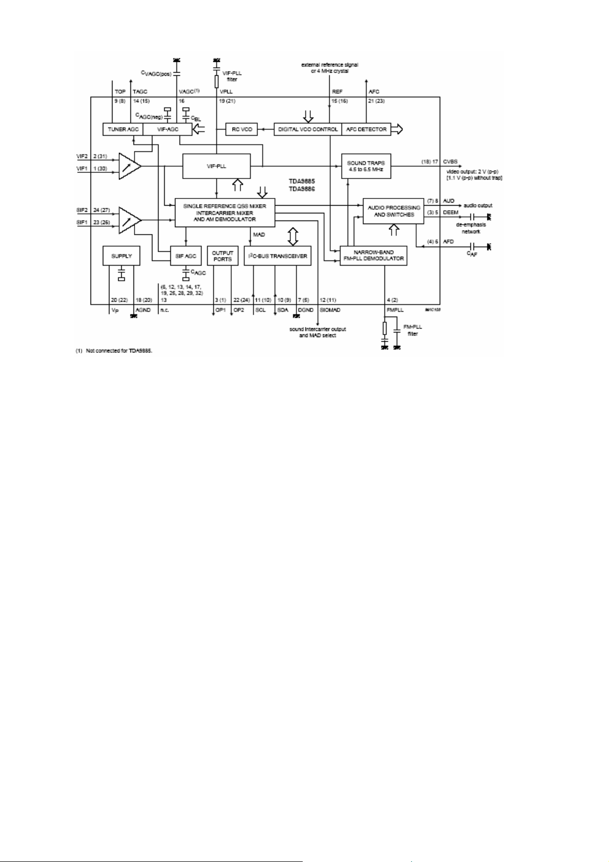
3. IF PART (TDA9886)
The TDA9886 is an alignment-free multistandard (PAL, SECAM and NTSC) vision and sound IF signal
PLL demodulator for positive and negative modulation, including sound AM and FM processing.
The following figure shows the simplified block diagram of the integrated circuit.
The integrated circuit comprises the following functional blocks:
VIF amplifier, Tuner and VIF-AGC, VIF-AGC detector, Frequency Phase-Locked Loop (FPLL) detector, VCO
and divider, Digital acquisition help and AFC, Video demodulator and amplifier, Sound carrier trap, SIF amplifier,
SIF-AGC detector, Single reference QSS mixer, AM demodulator, FM demodulator and acquisition help, Audio
amplifier and mute time constant,
I²C-bus transceivers and MAD (module address), Internal voltage stabilizer.
1
32” TFT TV Service Manual 06/03/2006
4. MULTI STANDARD SOUND PROCESSOR
The MSP34x0G family of single-chip Multistandard Sound Processors covers the sound processing of all
analog TV-Standards worldwide, as well as the NICAM digital sound standards. The full TV sound
processing, starting with analog sound IF signal-in, down to processed analog AF-out, is performed on a
single chip.
These TV sound processing ICs include versions for processing the multichannel television sound (MTS)
signal conforming to the standard recommended by the Broadcast Television Systems Committee (BTSC).
The DBX noise reduction, or alternatively, Micronas Noise Reduction (MNR) is performed alignment free.
Other processed standards are the Japanese FM-FM multiplex standard (EIA-J) and the FM Stereo Radio
standard.
Current ICs have to perform adjustment procedures in order to achieve good stereo separation for BTSC
and EIA-J. The MSP 34x1G has optimum stereo performance without any adjustments.
5. VIDEO SWITCH TEA6415
In case of three or more external sources are used, the video switch IC TEA6415 is used. The main
function of this device is to switch 8 video-input sources on the 6 outputs.
Each output can be switched on only one of each input. On each input an alignment of the lowest level of
the signal is made (bottom of sync. top for CVBS or black level for RGB signals).
Each nominal gain between any input and output is 6.5dB.For D2MAC or Chroma signal the alignment is
switched off by forcing, with an external resistor bridge, 5VDC on the input. Each input can be used as a
normal input or as a MAC or Chroma input (with external Resistor Bridge). All the switching possibilities are
changed through the BUS. Driving 75ohm load needs an external resistor. It is possible to have the same
input connected to several outputs.
6. AUDIO AMPLIFIER STAGE WITH TPA3002D2
The TPA3002D2 is a 9-W (per channel) efficient, Class-D audio amplifier for driving bridged-tied stereo
speakers. The TPA3002D2 can drive stereo speakersas low as 8 . The high efficiency of the TPA3002D2
eliminates the need for external heatsinks when playing music.
7. POWER
The LM2576 series of regulators are monolithic integrated circuits ideally suited for easy and convenient
design of a step–down switching regulator (buck converter). All circuits of this series are capable of driving
a 3.0A load with excellent line and load regulation. Two different versions (one having a fixed output
voltage of 3.3 V, and one with 5.0 V) of this IC are used in the regulator board.
2
32” TFT TV Service Manual 06/03/2006

8. MICROCONTROLLER SDA55XX
8.1. General Features
• Feature selection via special function register
• Simultaneous reception of TTX, VPS, PDC, and WSS (line 23)
• Supply Voltage 2.5 and 3.3 V
• ROM version is used.
8.2. External Crystal and Pro grammable Clock Speed
• Single external 6MHz crystal, all necessary clocks are generated internally
• CPU clock speed selectable via special function registers.
• Normal Mode 33.33 MHz CPU clock, Power Save mode 8.33 MHz
8.3. Microcontroller Features
• 8bit 8051 instruction set compatible CPU.
• 33.33-MHz internal clock (max.)
• 0.360 s (min.) instruction cycle
• Two 16-bit timers
• Watchdog timer
• Capture compare timer for infrared remote control decoding
• Pulse width modulation unit (2 channels 14 bit, 6 channels 8 bit)
• ADC (4 channels, 8 bit)
• UART (rxd, txd)
8.4. Memory
• Up to 128 Kilobyte on Chip Program ROM
• Eight 16-bit data pointer registers (DPTR)
• 256-bytes on-chip Processor Internal RAM (IRAM)
• 128bytes extended stack memory.
• Display RAM and TXT/VPS/PDC/WSS-Acquisition-Buffer directly accessible via MOVX
• UP to 16KByte on Chip Extended RAM (XRAM) consisting of;
- 1 Kilobyte on-chip ACQ-buffer-RAM (access via MOVX)
- 1 Kilobyte on-chip extended-RAM (XRAM, access via MOVX) for user software
- 3-Kilobyte Display Memory
8.5. Display Features
• ROM Character set supports all East and West European Languages in single device
• Mosaic Graphic Character Set
• Parallel Display Attributes
• Single/Double Width/Height of Characters
• Variable Flash Rate
• Programmable Screen Size (25 Rows x 33...64 Columns)
• Flexible Character Matrixes (HxV) 12 x 9...16
• Up to 256 Dynamical Redefinable Characters in standard mode; 1024 Dynamical Redefinable Characters
in Enhanced Mode
• CLUT with up to 4096 colour combinations
• Up to 16 Colours per DRCS Character
• One out of 8 Colours for Foreground and Background Colours for 1-bit DRCS and ROM Characters
8.6. ROM Characters
• Shadowing
• Contrast Reduction
• Pixel by Pixel Shiftable Cursor With up to 4 Different Colours
• Support of Progressive Scan and 100 Hz.
• 3 X 4Bits RGB-DACs On-Chip
• Free Programmable Pixel Clock from 10 MHz to 32MHz
• Pixel Clock Independent from CPU Clock
• Multinorm H/V-Display Synchronisation in Master or Slave Mode
3
32” TFT TV Service Manual 06/03/2006

8.7. Acquisition Features
• Multistandard Digital Data Slicer
• Parallel Multi-norm Slicing (TTX, VPS, WSS, CC, G+)
• Four Different Framing Codes Available
• Data Caption only limited by available Memory
• Programmable VBI-buffer
• Full Channel Data Slicing Supported
• Fully Digital Signal Processing
• Noise Measurement and Controlled Noise Compensation
• Attenuation Measurement and Compensation
• Group Delay Measurement and Compensation
• Exact Decoding of Echo Disturbed Signals
8.8. Ports
• One 8-bit I/O-port with open drain output and optional I 2 C Bus emulation support (Port0)
• Two 8-bit multifunction I/O-ports (Port1, Port3)
• One 4-bit port working as digital or analogue inputs for the ADC (Port2)
• One 2-bit I/O port with secondary function (P4.2, 4.3, 4.7)
• One 4-bit I/O-port with secondary function (P4.0, 4.1, 4.4) (Not available in P-SDIP 52)
9. SERIAL ACCESS CMOS 16K (2048*8) EEPROM ST24C16
The ST24C16 is a 16Kbit electrically erasable programmable memory (EEPROM), organised as 8 blocks
of 256*8 bits. The memory is compatible with the I²C standard, two wire serial interface, which uses a bidirectional data bus and serial clock. The memory carries a built-in 4 bit, unique device identification code
(1010) corresponding to the I²C bus definition. This is used together with 1 chip enable input (E) so that up
to 2*8K devices may be attached to the I²C bus and selected individually.
10. CLASS AB STEREO HEADPHONE DRIVER TDA1308
The TDA1308 is an integrated class AB stereo headphone driver contained in a DIP8 plastic package. The
device is fabricated in a 1 mm CMOS process and has been primarily developed for portable digital audio
applications.
11. SAW FILTERS
K3953M is an IF Filter for Video Applications. The package is SIP5K. Supported standards are B/G, D/K, I,
L/L’.
K9656M is an IF Filter for Audio Applications. The package is SIP5K. Supported standards are B/G, D/K, I,
L/L’.
4
32” TFT TV Service Manual 06/03/2006
12. IC DESCRIPTIONS AND INTERNAL BLOCK DIAGRAM
LM1117 TDA9886
LM2576 TDA1308T
LM317T PI5V330
ST24LC21 GM6015
TEA5114A AD9883A
TEA6415 MC141585
VPC3230D MC34063
SDA55XX MSP3410G
TPA3002D2 DS90C385
NDS8947
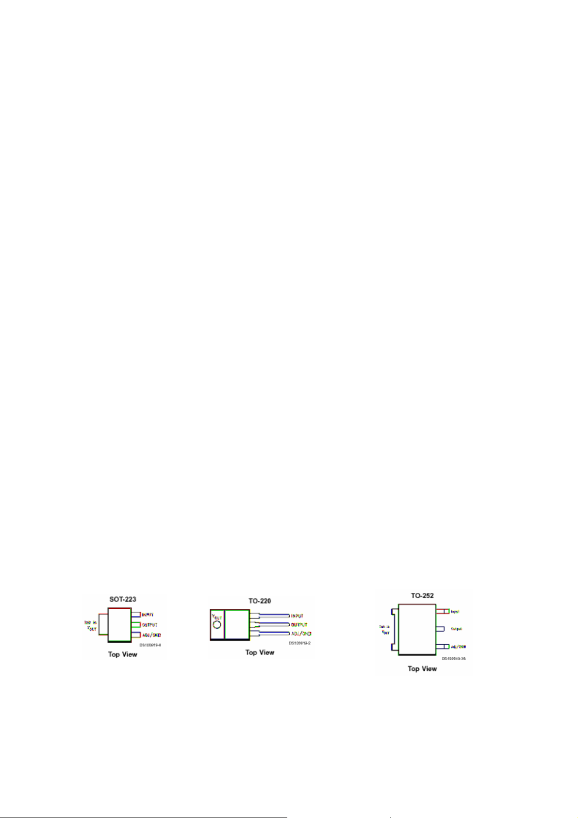
12.1. LM1117
12.1.1. General Description
The LM1117 is a series of low dropout voltage regulators with a dropout of 1.2V at 800mA of load current.
It has the same pin-out as National Semiconductor’s industry standard LM317. The LM1117 is available in
an adjustable version, which can set the output voltage from 1.25V to 13.8V with only two external
resistors. In addition, it is also available in five fixed voltages, 1.8V, 2.5V, 2.85V, 3.3V, and 5V.
The LM1117 offers current limiting and thermal shutdown. Its circuit includes a zener trimmed bandgap
reference to as-sure output voltage accuracy to within ±1%. The LM1117 series is available in SOT-223,
TO-220, and TO-252 D-PAK packages. A minimum of 10µF tantalum capacitor is required at the output to
improve the transient response and stability.
12.1.2. Features
• Available in 1.8V, 2.5V, 2.85V, 3.3V, 5V, and Adjustable Versions
• Space Saving SOT-223 Package
• Current Limiting and Thermal Protection
• Output Current 800mA
• Line Regulation 0.2% (Max)
• Load Regulation 0.4% (Max)
• Temperature Range
— LM1117 0°C to 125°C
— LM1117I -40°C to 125°C
12.1.3. Applications
• 2.85V Model for SCSI-2 Active Termination
• Post Regulator for Switching DC/DC Converter
• High Efficiency Linear Regulators
• Battery Charger
• Battery Powered Instrumentation
12.1.4. Connection Diagrams
5
32” TFT TV Service Manual 06/03/2006
12.2. LM2576
12.2.1. General Description
The LM2576 series of regulators are monolithic integrated circuits ideally suited for easy and convenient
design of a step–down switching regulator (buck converter). All circuits of this series are capable of driving
a 3.0 A load with excellent line and load regulation.
These devices are available in fixed output voltages of 3.3 V, 5.0 V, 12 V, 15 V, and an adjustable output
version. These regulators were designed to minimize the number of external components to simplify the
power supply design. Standard series of inductors optimized for use with the LM2576 are offered by
several different inductor manufacturers.
Since the LM2576 converter is a switch–mode power supply, its efficiency is significantly higher in
comparison with popular three–terminal linear regulators, especially with higher input voltages. In many
cases, the power dissipated is so low that no heatsink is required or its size could be reduced dramatically.
A standard series of inductors optimized for use with the LM2576 are available from several different
manufacturers. This feature greatly simplifies the design of switch–mode power supplies.
The LM2576 features include a guaranteed ±4% tolerance on output voltage within specified input voltages
and output load conditions, and ±10% on the oscillator frequency (±2% over 0°C to 125°C). External
shutdown is included, featuring 80 mA (typical) standby current. The output switch includes cycle–by–cycle
current limiting, as well as
thermal shutdown for full protection under fault conditions.
12.2.2. Features
• 3.3 V, 5.0 V, 12 V, 15 V, and Adjustable Output Versions
• Adjustable Version Output Voltage Range, 1.23 to 37 V ±4% Maximum Over Line and Load Conditions
• Guaranteed 3.0 A Output Current
• Wide Input Voltage Range
• Requires Only 4 External Components
• 52 kHz Fixed Frequency Internal Oscillator
• TTL Shutdown Capability, Low Power Standby Mode
• High Efficiency
• Uses Readily Available Standard Inductors
• Thermal Shutdown and Current Limit Protection
• Moisture Sensitivity Level (MSL) Equals 1
12.2.3. Pin description
6
32” TFT TV Service Manual 06/03/2006

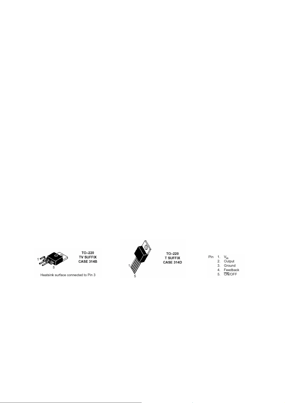
12.3. LM317T
12.3.1. Description
The LM317T is an adjustable 3 terminal positive voltage regulator capable of supplying in excess of 1.5
amps over an output range of 1.25 to 37 volts. This voltage regulator is exceptionally easy to use and
requires only two external resistors to set the output voltage. Further, it employs internal current limiting,
thermal shutdown and safe area compensation, making it essentially blow–out proof. The LM317 serves a
wide variety of applications including local, on card regulation. This device can also be used to make a
programmable output regulator, or by connecting a fixed resistor between the adjustment and output, the
LM317 can be used as a precision current regulator.
12.3.2. Features
• Output Current in Excess of 1.5 A
• Output Adjustable between 1.2 V and 37 V
• Internal Thermal Overload Protection
• Internal Short Circuit Current Limiting Constant with Temperature
• Output Transistor Safe–Area Compensation
• Floating Operation for High Voltage Applications
• Available in Surface Mount D
2
PAK, and Standard 3–Lead Transistor Package
• Eliminates Stocking many Fixed Voltages
7
32” TFT TV Service Manual 06/03/2006
12.4. ST24LC21
12.4.1. Description
The ST24LC21 is a 1K bit electrically erasable programmable memory (EEPROM), organized by 8 bits.
This device can operate in two modes: Transmit Only mode and I
2
C bidirectional mode. When powered,
the device is in Transmit Only mode with EEPROM data clocked out from the rising edge of the signal
applied on VCLK. The device will switch to the I
applied on SCL pin. The ST24LC21 can not switch from the I
2
C bidirectional mode upon the falling edge of the signal
2
C bidirectional mode to the Transmit Only
mode (except when the power supply is removed). The device operates with a power supply value as low
as 2.5V. Both Plastic Dual-in-Line and Plastic Small Outline packages are available.
12.4.2. Features
• 1 million Erase/Write cycles
• 40 years data retention
• 2.5V to 5.5V single supply voltage
• 400k Hz compatibility over the full range of supply voltage
• Two wire serial interface I
2
C bus compatible
• Page Write (Up To 8 Bytes)
• Byte, random and sequential read modes
• Self timed programming cycle
• Automatic address incrementing
• Enhanced ESD/Latch up
• Performances
12.4.3. Pin connections
DIP Pin connections CO Pin connections
NC: Not connected
Signal names
SDA Serial data Address Input/Output
SCL Serial Clock (I2C mode)
Vcc Supply voltage
Vss Ground
VCLK Clock transmit only mode
8
32” TFT TV Service Manual 06/03/2006
12.5. TEA5114A
12.5.1. General description
This integrated circuit provides RGB switching allowing connections between peri TV plug, internal RGB
generator and video processor in a TV set.
The input signal black level is tied to the same reference voltage on each input in order to have no
differential voltage when switching two RGB generators.
An AC output signal higher than 2 Vpp makes gain going slowly down to 0dBto protect the TV set video
amplifier from saturation.
Fast blanking output is a logical OR between FB1 (Pin 8) and FB2 (Pin 10).
12.5.2. Features
• 25MHz Bandwidth
• Crosstalk : 55dB
• Short circuit to ground or V
CC protected
• Anti saturation gain changing
• Video switching
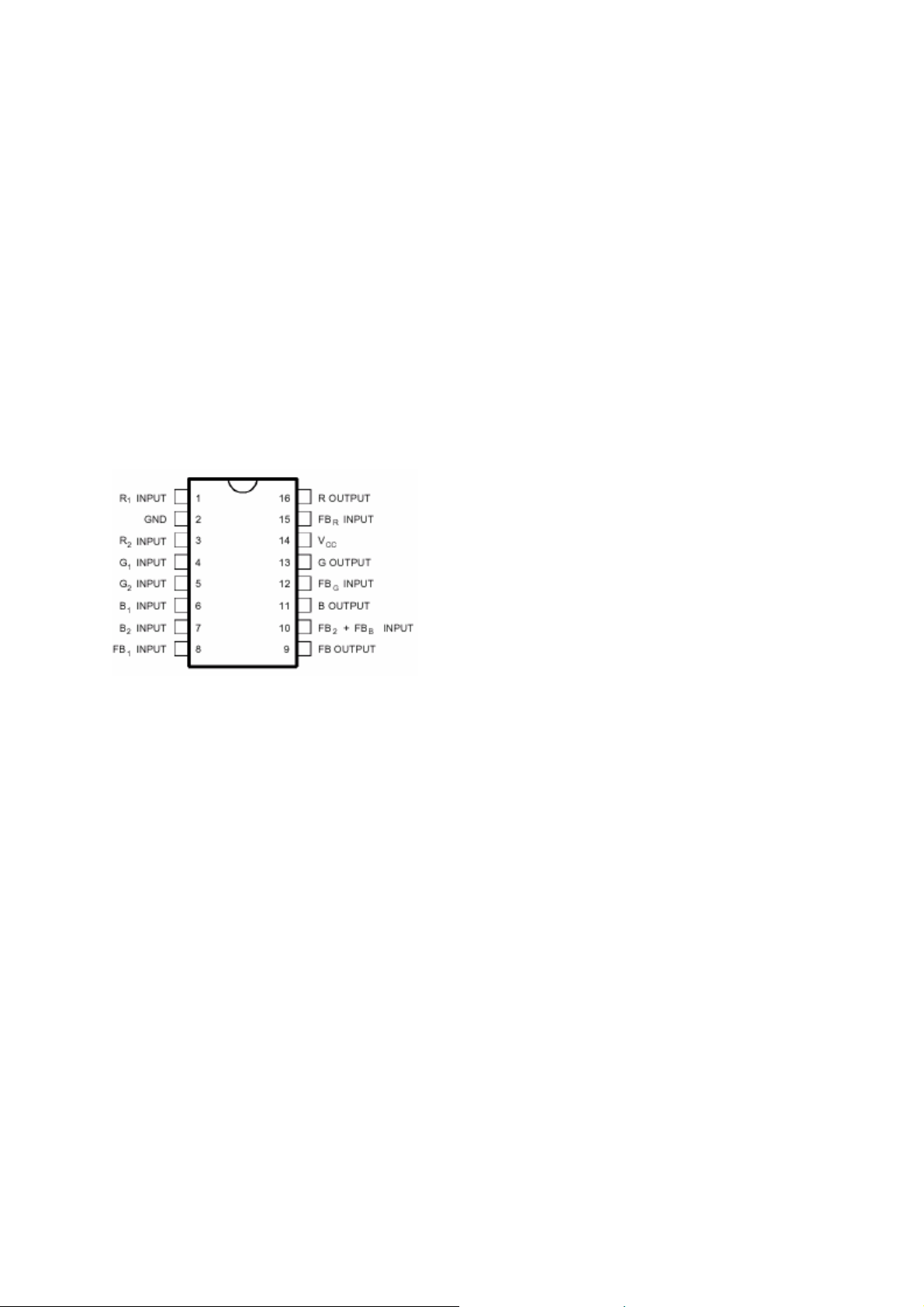
12.5.3. Pin Connections
9
32” TFT TV Service Manual 06/03/2006

12.6. TEA6415
12.6.1. General description
The main function of the IC is to switch 8 video input sources on 6 outputs. Each output can be switched
on only one of each input. On each input an alignment of the lowest level of the signal is made (bottom of
synch. top for CVBS or black level for RGB signals). Each nominal gain between any input and output is
6.5dB. For D2MAC or Chroma signal the alignment is switched off by forcing, with an external resistor
bridge, 5 V
DC on the input. Each input can be used as a normal input or as a MAC or Chroma input (with
external resistor bridge). All the switching possibilities are changed through the BUS. Driving 75 load
needs an external transistor. It is possible to have the same input connected to several outputs. The
starting configuration upon power on (power supply: 0 to 10V) is undetermined. In this case, 6 words of 16
bits are necessary to determine one configuration. In other case, 1 word of 16 bits is necessary to
determine one configuration.
12.6.2. Features
• 20MHz Bandwidth
• Cascadable with another TEA6415C (Internal address can be changed by pin 7 voltage)
• 8 Inputs (CVBS, RGB, MAC, CHROMA,...)
• 6 Outputs
• Possibility of MAC or chroma signal for each input by switching-off the clamp with an external resistor
bridge
• Bus controlled
• 6.5dB gain between any input and output
• 55dB crosstalk at 5mHz
• Fully ESD protected
12.6.3. Pinning
1. Input : Max : 2Vpp, Input Current: 1mA, Max : 3mA
2. Data : Low level : -0.3V Max: 1.5V,
High level : 3.0V Max : Vcc+0.5V
3. Input : Max : 2Vpp, Input Current: 1mA, Max : 3mA
4. Clock : Low level : -0.3V Max: 1.5V,
High level : 3.0V Max : Vcc+0.5V
5. Input : Max : 2Vpp, Input Current: 1mA, Max : 3mA
6. Input : Max : 2Vpp, Input Current: 1mA, Max : 3mA
7. Prog
8. Input : Max : 2Vpp, Input Current: 1mA, Max: 3mA
9. Vcc : 12V
10. Input : Max : 2Vpp, Input Current: 1mA, Max : 3mA
11. Input : Max : 2Vpp, Input Current: 1mA, Max : 3mA
12. Ground
13. Output : 5.5Vpp, Min : 4.5Vpp
14. Output : 5.5Vpp, Min : 4.5Vpp
15. Output : 5.5Vpp, Min : 4.5Vpp
16. Output : 5.5Vpp, Min : 4.5Vpp
17. Output : 5.5Vpp, Min : 4.5Vpp
18. Output : 5.5Vpp, Min : 4.5Vpp
19. Ground
20. Input : Max : 2Vpp, Input Current : 1mA, Max : 3mA
10
32” TFT TV Service Manual 06/03/2006
12.7. VPC3230D
12.7.1. General Description
The VPC 323xD is a high-quality, single-chip video front-end, which is targeted for 4:3 and 16:9, 50/60-Hz
and 100/120 Hz TV sets. It can be combined with other members of the DIGIT3000 IC family (such as
DDP 331x) and/or it can be used with 3rd-party products.
The main features of the VPC 323xD are
• high-performance adaptive 4H comb filter Y/C separator with adjustable vertical peaking
• multi-standard colour decoder PAL/NTSC/SECAM including all substandards
• four CVBS, one S-VHS input, one CVBS output
• two RGB/YC
r Cb component inputs, one Fast Blank (FB) input
• integrated high-quality A/D converters and associated clamp and AGC circuits
• multi-standard sync processing
• linear horizontal scaling (0.25 ... 4), as well as non-linear horizontal scaling ‘Panorama-vision’
• PAL+ preprocessing
• line-locked clock, data and sync, or 656-output interface
• peaking, contrast, brightness, color saturation and tint for RGB/ YC
r C b and CVBS/ S-VHS
• high-quality soft mixer controlled by Fast Blank
• PIP processing for four picture sizes (1/4, 1/9, 1/16 or 1/36 of normal size) with 8-bit resolution
• 15 predefined PIP display configurations and expert mode (fully programmable)
• control interface for external field memory
2
• I
C-bus interface
• one 20.25-MHz crystal, few external components
• 80-pin PQFP package
12.7.2. Pin Connections and Short Descriptions
NC = not connected
LV = if not used, leave vacant
X = obligatory; connect as described in circuit diagram
SUPPLYA = 4.75...5.25 V, SUPPLYD = 3.15...3.45 V
Pin No.
PQFP
80-pin
1 B1/CB1IN IN VREF Blue1/Cb1 Analog Component Input
2 G1/Y1IN IN VREF Green1/Y1 Analog Component Input
3 R1/CR1IN IN VREF Read1/Cr1 Analog Component Input
4 B2/CB2IN IN VREF Blue2/Cb2 Analog Component Input
5 G2/Y2IN IN VREF Green2/Y2 Analog Component Input
6 R2/CR2IN IN VREF Read2/Cr2 Analog Component Input
7 ASGF X Analog Shield GNDF
8 FFRSTWIN IN LV or GNDD FIFO Reset Write Input
9 V
10 V
11 GNDD SUPPLYD X Ground, Digital Circuitry
12 GND
13 SCL IN/OUT X I2C Bus Clock
14 SDA IN/OUT X I2C Bus Data
15 RESQ IN X Reset Input, Active Low
16 TEST IN GNDD Test Pin, connect to GNDD
17 VGAV IN GNDD VGAV Input
18 YCOEQ IN GNDD Y/C Output Enable Input, Active Low
19 FFIE OUT LV FIFO Input Enable
20 FFWE OUT LV FIFO Write Enable
21 FFRSTW OUT LV FIFO Reset Write/Read
22 FFRE OUT LV FIFO Read Enable
23 FFOE OUT LV FIFO Output Enable
24 CLK20 IN/OUT LV Main Clock output 20.25 MHz
25 GNDPA OUT X Pad Decoupling Circuitry GND
26 V
27 LLC2 OUT LV Double Clock Output
28 LLC1 IN/OUT LV Clock Output
29 V
Pin Name Type Connection
(if not used)
OUT X Digital Decoupling Circuitry Supply Voltage
SUPCAP
SUPPLYD X Supply Voltage, Digital Circuitry
SUPD
OUT X Digital Decoupling Circuitry GND
CAP
OUT X Pad Decoupling Circuitry Supply Voltage
SUPPA
SUPPLYD X Supply Voltage, LLC Circuitry
SUPLLC
Short Description
11
32” TFT TV Service Manual 06/03/2006

30 GND
SUPPLYD X Ground, LLC Circuitry
LLC
31 Y7 OUT GNDY Picture Bus Luma (MSB)
32 Y6 OUT GNDY Picture Bus Luma
33 Y5 OUT GNDY Picture Bus Luma
34 Y4 OUT GNDY Picture Bus Luma
35 GNDY SUPPLYD X Ground, Luma Output Circuitry
36 V
SUPPLYD X Supply Voltage, Luma Output Circuitry
SUPY
37 Y3 OUT GNDY Picture Bus Luma
38 Y2 OUT GNDY Picture Bus Luma
39 Y1 OUT GNDY Picture Bus Luma
40 Y0 OUT GNDY Picture Bus Luma (LSB)
41 C7 OUT GNDC Picture Bus Chroma (MSB)
42 C6 OUT GNDC Picture Bus Chroma
43 C5 OUT GNDC Picture Bus Chroma
44 C4 OUT GNDC Picture Bus Chroma
45 V
SUPPLYD X Supply Voltage, Chroma Output Circuitry
SUPC
46 GNDC SUPPLYD X Ground, Chroma Output Circuitry
47 C3 OUT GNDC Picture Bus Chroma
48 C2 OUT GNDC Picture Bus Chroma
49 C1 OUT GNDC Picture Bus Chroma
50 C0 OUT GNDC Picture Bus Chroma (LSB)
51 GNDSY SUPPLYD X Ground Sync Pad Circuitry
52 V
SUPPLYD X Supply Voltage, Sync Pad Circuitry
SUPSY
53 INTLC OUT LV Interlace Output
54 AVO OUT LV Active Video Output
55 FSY/HC/HSYA OUT LV Front Sync/ Horizontal Clamp Pulse/Front-End
Horizontal Sync Output
56 MSY/HS IN/OUT LV Main Sync/Horizontal Sync Pulse
57 VS OUT LV Vertical Sync Pulse
58 FPDAT/VSYA IN/OUT LV Front End/Back-End Data/Front-End Vertical Sync
Output
59 V
SUPPLYA X Standby Supply Voltage
STBYY
60 CLK5 OUT LV CCU 5 MHz Clock Output
61 NC - LV or GNDD Not Connected
62 XTAL1 IN X Analog Crystal Input
63 XTAL2 OUT X Analog Crystal Output
64 ASGF X Analog Shield GNDF
65 GNDF SUPPLYA X Ground, Analog Front-End
66 VRT OUTPUT X Reference Voltage Top, Analog
67 I2CSEL IN X I2C Bus Address Select
68 ISGND SUPPLYA X Signal Ground for Analog Input, connect to GNDF
69 V
SUPPLYA X Supply Voltage, Analog Front-End
SUPF
70 VOUT OUT LV Analog Video Output
71 CIN IN LV Chroma/Analog Video 5 Input
72 VIN1 IN VRT Video 1 Analog Input
73 VIN2 IN VRT Video 2 Analog Input
74 VIN3 IN VRT Video 3 Analog Input
75 VIN4 IN VRT Video 4 Analog Input
76 V
SUPPLYA X Supply Voltage, Analog Component Inputs Front-End
SUPAI
77 GNDAI SUPPLYA X Ground, Analog Component Inputs Front-End
78 VREF OUTPUT X Reference Voltage Top, Analog Component Inputs
Front-End
79 FB1IN IN VREF Fast Blank Input
80 AISGND SUPPLYA X Signal Ground for Analog Component Inputs, connect
to GND
AI
12
32” TFT TV Service Manual 06/03/2006

12.8. SDA55XX (SDA5550)
12.8.1. General description
The SDA55XX is a single chip teletext decoder for decoding World System Teletext data as well as Video
Programming System (VPS), Program Delivery Control (PDC), and Wide Screen Signalling (WSS) data
used for PAL plus transmissions (Line 23). The device also supports Closed caption acquisition and
decoding. The device provides an integrated general-purpose, fully 8051-compatible Microcontroller with
television specific hardware features. Microcontroller has been enhanced to provide powerful features such
as memory banking, data pointers, and additional interrupts etc. The on-chip display unit for displaying
Level 1.5 teletext data can also be used for customer defined on screen displays. Internal XRAM consists
of up to16 Kbytes. Device has an internal ROM of up to 128 KBytes. ROMless versions can access up to 1
MByte of external RAM and ROM. The SDA 55XX supports a wide range of standards including PAL,
NTSC and contains a digital slicer for VPS, WSS, PDC, TTX and Closed Caption, an accelerating
acquisition hardware module, a display generator for Level 1.5 TTX data and powerful On screen Display
capabilities based on parallel attributes, and Pixel oriented characters (DRCS).
The 8-bit Microcontroller runs at 360 ns. cycle time (min.). Controller with dedicated hardware does most of
the internal TTX acquisition processing, transfers data to/from external memory interface and receives/
transmits data via I
2
C-firmware user-interface. The slicer combined with dedicated hardware stores TTX
data in a VBI buffer of 1 Kilobyte. The Microcontroller firmware performs all the acquisition tasks (hamming
and parity-checks, page search and evaluation of header control bits) once per field. Additionally, the
firmware can provide high-end Teletext features like Packet-26-handling, FLOF, TOP and list-pages. The
interface to user software is optimized for minimal overhead. SDA 55XX is realized in 0.25 micron
technology with 2.5 V supply voltage and 3.3 V I/O (TTL compatible). The software and hardware
development environment (TEAM) is available to simplify and speed up the development of the software
and On Screen Display. TEAM stands for TVT Expert Application Maker. It improves the TV controller
software quality in following aspects:
– Shorter time to market
– Re-usability
– Target independent development
– Verification and validation before targeting
– General test concept
– Graphical interface design requiring minimum programming and controller know how.
– Modular and open tool chain, configurable by customer.
13
32” TFT TV Service Manual 06/03/2006
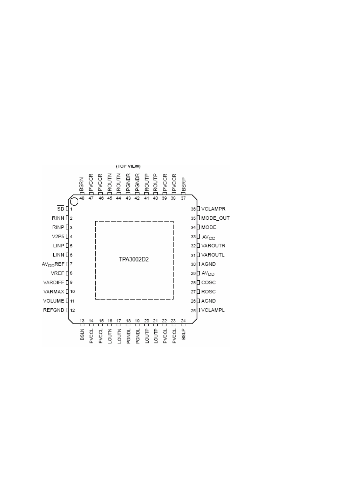
12.9. TPA3003D2
12.9.1. General Description
The TPA3002D2 is a 9-W (per channel) efficient, Class-D audio amplifier for driving bridged-tied stereo
speakers. The TPA3002D2 can drive stereo speakers as low as 8 &. The high efficiency of the
TPA3002D2 eliminates the need for external heatsinks when playing music.
12.9.2. Features
- 9-W/Ch Into an 8- Load From 12-V Supply
- Efficient, Class-D Operation Eliminates Heatsinks and Reduces Power Supply Requirements
- 32-Step DC Volume Control From –40 dB to 36 dB
- Line Outputs For External Headphone
- Amplifier With Volume Control
- Regulated 5-V Supply Output for Powering TPA6110A2
- Space-Saving, Thermally-Enhanced PowerPAD Packaging
- Thermal and Short-Circuit Protection
12.9.3. Pin Connection
14
32” TFT TV Service Manual 06/03/2006
 Loading...