

Vestel 17MB18-5 23 Schematic

TABLE OF CONTENTS
1. SOFTWARE UPDATE DESCRIPTION .................................................................................................1
2. INTRODUCTION ...................................................................................................................................4
2.1. Scope .................................................................................................................................................4
2.2. General Features ...............................................................................................................................4
3. SYSTEM BUILDING BLOCKS ..............................................................................................................5
3.1. Analog Front End ...............................................................................................................................5
3.1.1. Tuner...........................................................................................................................................5
3.1.2. SAW Filters .................................................................................................................................6
3.2. Back End ............................................................................................................................................6
3.3. Side Board(s) .....................................................................................................................................9
3.3.1. Keypads......................................................................................................................................9
3.3.2. IR&Led Board .............................................................................................................................9
3.4. Power ...............................................................................................................................................10
4. IC AND COMPONENT DESCRIPTIONS ............................................................................................12
4.1. Basic IC List .....................................................................................................................................12
4.2. UOCIII ..............................................................................................................................................12
4.2.1. Pinout........................................................................................................................................13
4.3. PW1306 ...........................................................................................................................................17
4.3.1. Pinout........................................................................................................................................17
4.4. M29W800AT ....................................................................................................................................26
4.5. DS90C385........................................................................................................................................26
4.6. P15V330 ..........................................................................................................................................26
4.7. 74HC4052 ........................................................................................................................................26
4.8. TA1366FG........................................................................................................................................27
4.9. TDA7056A........................................................................................................................................27
4.10. TDA1308 ......................................................................................................................................27
4.11. LM1117.........................................................................................................................................28
4.12. 24LC32.........................................................................................................................................28
4.13. 24LC21.........................................................................................................................................28
4.14. 74LVC541.....................................................................................................................................29
4.15. SAA3010T ....................................................................................................................................29
4.16. MC34167 ......................................................................................................................................30
4.17. TFMS5360....................................................................................................................................30
4.18. Board Connectors, Headers & Jumpers.......................................................................................30
4.18.1. Analog PC Connector (PL400)..............................................................................................30
4.18.2. Scart Connector (PL401) ......................................................................................................31
4.18.3. S-Video Connector (JK403) ..................................................................................................31
4.18.4. LVDS Panel Connector(1x20 PL179) ...................................................................................31
4.18.5. TTL Panel Connector -Even (2x17 PL177)...........................................................................32
4.18.6. TTL Panel Connector -Odd (2x17 PL178) ............................................................................32
4.18.7. Panel Inverter Connector (1x11 PL176) ...............................................................................32
4.18.8. Keypad Card Connector (1x5 PL175)...................................................................................33
4.18.9. Optional Keypad Connector to UOC (1x2 PL 202) ...............................................................33
4.18.10. LED & IR Receiver Connector (1x6 PL202)..........................................................................33
4.18.11. Optional Rocker Sw. Connector (1x4 PL500) .......................................................................33
4.18.12. PROMJet Connector (2x25 PL101) ......................................................................................33
4.18.13. Side HP Connector for Side-card Option (PL405) ................................................................33
4.18.14. Side AV Connector for Side-card Option (PL406) ................................................................34
4.18.15. Side SVHS Connector for Side-card Option (PL407) ...........................................................34
5. DIGITAL MODULE IC and CONNECTOR DESCRIPTIONS ..............................................................35
5.1. STI5518............................................................................................................................................35
5.1.1. General Description................................................................................................................35
5.2. MAX232_SMD .................................................................................................................................35
5.2.1. General Description................................................................................................................35
5.2.2. Features ...................................................................................................................................35
5.3. 74HCU04 .........................................................................................................................................36
5.3.1. General Description................................................................................................................36
i
i
TFT TV Service Manual

5.3.2. Pin Description........................................................................................................................36
5.4. TSH22 ..............................................................................................................................................37
5.4.1. General Description................................................................................................................37
5.4.2. Pin Connections......................................................................................................................37
5.5. CS4334 ............................................................................................................................................37
5.5.1. General Description................................................................................................................37
5.5.2. Features ...................................................................................................................................37
5.6. AMIC A43L2616...............................................................................................................................38
5.6.1. General Description................................................................................................................38
5.6.2. Features ...................................................................................................................................38
5.6.3. Pin Description........................................................................................................................38
5.7. MX29LV160T ...................................................................................................................................40
5.7.1. General Description................................................................................................................40
5.7.2. Features ...................................................................................................................................40
5.7.3. Pin Description........................................................................................................................40
5.8. 24C32...............................................................................................................................................41
5.8.1. General Description................................................................................................................41
5.8.2. Features ...................................................................................................................................41
5.8.3. Pin Description........................................................................................................................41
5.9. STV0360 ..........................................................................................................................................42
5.9.1. General Description................................................................................................................42
5.9.2. Features ...................................................................................................................................42
5.9.3. Pin Description........................................................................................................................42
5.10. MAX809........................................................................................................................................45
5.10.1. General Description ............................................................................................................45
5.10.2. Features ...............................................................................................................................45
5.10.3. Pin Description....................................................................................................................45
5.11. TDCC2345TV39A.........................................................................................................................46
5.11.1. General Description ............................................................................................................46
5.11.2. Pin Description....................................................................................................................46
5.12. STV0700.......................................................................................................................................46
5.12.1. General description ............................................................................................................46
5.12.2. Features ...............................................................................................................................47
5.12.3. Pin Description....................................................................................................................47
5.13. 74HC373 ......................................................................................................................................52
5.13.1. General Description ............................................................................................................52
5.13.2. Pin Connections ..................................................................................................................52
5.14. 74HC245 ......................................................................................................................................52
5.14.1. General Description ............................................................................................................52
5.14.2. Features ...............................................................................................................................52
6. SERVICE MENU SETTINGS ..............................................................................................................53
6.1. UOCIII Service Menu .......................................................................................................................53
6.1.1. UOCIII Service Menu Settings ...............................................................................................53
6.1.2. Tuner AGC Alignment...............................................................................................................57
6.1.3. DCXO Alignment.......................................................................................................................57
6.2. PW1306 Service Menu ....................................................................................................................57
6.2.1. UOC Horizontal Position...........................................................................................................58
6.2.2. UOC Calibration........................................................................................................................58
6.2.3. PW1306 PC Input ADC Calibration ..........................................................................................58
6.2.4. Init NVM ....................................................................................................................................59
6.2.5. Initial APS .................................................................................................................................59
6.2.6. Hotel Mode Activate..................................................................................................................59
6.2.7. Burn-In Mode ............................................................................................................................59
6.2.8. Country .....................................................................................................................................59
6.2.9. Language ..................................................................................................................................59
6.2.10. Menu Background .................................................................................................................60
6.2.11. Remote Control .....................................................................................................................60
6.3. Panel Type Change Shortcut...........................................................................................................60
7. PRODUCTION SETTINGS AND FACTORY DEFAULTS...................................................................61
7.1. Production Schedule........................................................................................................................61
iiii

7.2. EEPROM Settings............................................................................................................................61
7.2.1. Creating Master EEPROM........................................................................................................61
7.2.2. Creating Mass Production EEPROM ........................................................................................61
7.3. TV Menu...........................................................................................................................................61
7.3.1. Picture Menu.............................................................................................................................61
7.3.2. Audio Menu .............................................................................................................................61
7.3.3. Window Menu ...........................................................................................................................62
7.3.4. Options Menu............................................................................................................................62
7.3.5. Settings Menu ...........................................................................................................................62
7.4. PC Mode Menu ................................................................................................................................62
7.4.1. Picture Menu.............................................................................................................................62
7.4.2. Audio Menü...............................................................................................................................63
7.4.3. Window Menu ...........................................................................................................................63
7.4.4. Options Menü............................................................................................................................63
8. BLOCK DIAGRAM...............................................................................................................................65
9. CIRCUIT DIAGRAMS ..........................................................................................................................67
9.1. 17MB18-5 Main Board Schematics .................................................................................................67
9.2. Keypad Schematics .........................................................................................................................72
9.3. IR&LED Board Schematics ..............................................................................................................73
9.4. Remote Controller Schematics ........................................................................................................74
9.5. Digital Module Schematics...............................................................................................................75
9.6 Print Lay-outs(Analog Board)...........................................................................................................80
9.7 Print Lay-outs(Digital Board)............................................................................................................89
10. SPARE PART LIST .............................................................................................................................94
10.1 Analog Side Spare List......................................................................................................................94
10.2 Digital Side Spare List.....................................................................................................................108
11. Panel&Component Change List......................................................................................................109
iiiiii

1. SOFTWARE UPDATE DESCRIPTION
1
1. IC Programming
17MB18 has two programmable ICs, UOCIII (IC203) and 29XX800 (IC102, having the
PW1306 (IC100) codes).
29XX800 (IC102) will be programmed before the TV production and will be mounted as
programmed. On the other hand, software update can be needed after production so the
programming instructions is given also for this IC in related chapter.
1.1. UOC III Programming
Step 1: Entering to ISP Mode
1. Press Power On and turn on the TV.
2. Press Remote Controls (RC) “Menu” (M) and “4””7””2””5” buttons respe ctively.
3. The following menu will displayed on the screen.
4. Press RCs “0” ”0” ”2” buttons respectively.(“ISP Mode 0” line will be displayed on the
screen.)
5. Press RCs “Volume +” button and set UOC to ISP mode. .(“ISP Mode 1” line will be
displayed on the screen.)
GTV 3.2.1
000 EurAsia TVSub 05.01
00000000 00111100
01000000 01100100
11000101 01100100
00000000 01100100
Step 2: Loading the Code
1- Connect the 5 pin cable of the “programming board” to PL203 of the 17MB18 mainboard.
Connect the programming board to the computer in which “WISP” program is loaded via
“Paralel Port”.
2- Run WISP program. As it is seen in figure1 change “Delay time” value to “5” ms.
3- Under “Settings Menu”, set the I2C configurations as it is seen in figure2; press
“Confirm” and close this window.
(Note: Once the above settings are done, there is no need to do them again each time
loading the UOC code.)
4- Click “Enter ISP Mode” button and then click “Send” button. In the white display area
with “ISP status” heading, “ISP mode... Ready” will be displayed. (Unless you do not see
this warning, check the cable connections and the settings described above.)
Figure1: WISP Main Menu
2
Figure2: I2C Configuration
5- Click “Erase Flash” button and then click “Send” button. If ereasing is done without any
problem, “three green OK” will be displayed on the main menu window. This indicates
that the memory inside the IC is erased succesfully.
6- Click “Write Flash” button and then click “Browse” button. Select the “gtv.hex” UOC code
file by browsing the explorer to the folder where this “gtv.hex” file is stored. Wait for a
few seconds untill the program reads the code. You will see the blue bar indicating the
“reading operation” on the bottom of the Wisp main menu window.
7- Click “Send” button. You will see the blue bar indicating the “Loading Code to UOC IC”
on the bottom of the window. When the loading operation is over without any error
“three green OK” will be displayed on the window. This indicates the loading operation is
performed succesfully.
Step3: Initializing the TV
8- Turn off and on the TV. Press RCs “Menu” (M) and “4””7””2””5” buttons respectively.
9- Press RCs “0” ”0” ”1” buttons respectively. (“Init TV 0” will be displayed on the screen)
10- Press RCs “Volume +” and set “Init TV 1” and wait the TV to automatically turn off.
3
1.2. 29XX800 Programming for PW1306
The following instructions are only needed for software upgrades. For the TV production,
pre-programmed 29XX800 will be mounted on the board.
1- Copy flasher.hex and romcode.hex to “X:\XXX \ QTV_TVK2_V_021\Project\PW13XX_QTV”
directory.
2- Connect programmer board 4-pin cable to PL100 on 17MB18.
3- Connect programmer board serial port cable to PC COM Port1.
4- Close jumper PL501.
5- Execute “FlashUpgrader.exe” in “C:\XXX\ QTV_TVK2_V_021\bin\” directory.
6- Press “Choose” and select romcode.inf from
“C:\XXX\ QTV_TVK2_V_021\Project\PW13XX_QTV” directory.
7- Press “Flash”
8- Power on the board. Observe the sliding bar on the main menu showing that flasher.hex
and then romcode.hex are being downloaded to the IC on 17MB18 main board.
9- Power off the board when the download operation is over.
10- Open jumper PL501.
11- Power On the board. Press Remote Controls (RC) “Menu” (M) and “4””7””2””6” buttons
respectively.
12- By using RIGHT and LEFT buttons of the RC, select “Service Submenu 2”
13- By using DOWN button of the RC highlight Init NVM. Press RIGHT button of the RC and
initialize the PixelWorks side.
14- Turn Off and On the TV.
15- Depanding the size of the Panel(15”, 17”, 20”) the screen may be full white and no
picture is observed.
If screen is full white:
For 15” TV, Press Remote Controls (RC) “Menu” (M) and “4” “7” “2” “6” buttons and then “0”
respectively.
For 17” TV, Press Remote Controls (RC) “Menu” (M) and “4” “7” “2” “6” buttons and then “2”
respectively.
For 20” TV, Press Remote Controls (RC) “Menu” (M) and “4” “7” “2” “6” buttons and then “1”
respectively.

2. INTRODUCTION
2.1. Scope
The document covers 2
3” TFT 17MB18 chassis building blocks, basic features, service menu
settings, and the other information needed by service personal.
2.2. General Features
The system is a 14” to 23” TFT LCD TV solution with UOCIII Versatile Signal Processor and PW1306 Video Image
Processor chip-set on 4-layer PCB. The TV will support PAL/SECAM B/G/D/K/I/L/L’.
The other general default features of the TV are as listed below:
1 Full Scart input (with SVHS support)
1 SVHS input through standard S-Video interface.
1 CVBS input through standard RCA jack
75 ohms antenna input
D-Sub 15 PC Input
GERMAN + NICAM STEREO
<3W S/B Power Consumption from mains supply
2x3W Speaker Output Power @16 Ohm spks; HP Output, Stereo Audio line out
Stereo Audio line in
Equalizer
IR Control (RC5)
OSD;Menu Languages ENG, FRA, GER, ITA, SPA, POR, TUR, SWE, DEN, FIN, CRO, SLO, SLOVEN, NOR,
POL, CZE, HUN,ROM,BUL, RUS (subject to change and be grouped)
Teletext
2H/4H Comb Filter
White balance settings (warm/normal/cool) for TV&PC
Full AIR&CABLE band coverage
Auto Shut down
44

3. SYSTEM BUILDING BLOCKS
17MB18 chassis main blocks are as follows:
Analog Front End : UOCIII (Microcontroller + Video Proccessor + Sound Proccessor + IF), CTI, Tuner, SAW
filters, Audio Amp., DAC
Back End : PW1306(Microcontroller, Scaler, OSD, Keyboard/IR Interface)
Side Board(s) : Keyboards, IR/LED Boards, TTL Panel Interface Cards, VCbCr Input Board (Optional)
3.1. Analog Front End
17MB18 Main Board consists of two major blocks. The first block is analog front-end and this block is handled by
UOCIII chip that is highly multifunctional. This IC does demodulation of Video & Audio from Tuner IF, CVBS, Audio,
RGB, SVHS input selection and processing. It has an audio processor that supports equalizer or tone control, volume
control, AVL, surround effect etc and supplies amplifier, headphone and CVBS & audio line outputs. It handles video
processing such as colour standard detection and demodulation, picture alignment (brightness, contrast, colour etc.). The
IC also does teletext decoding with 10 pages text memory. After video processing, the processed video is applied to
PW1306 chip in RGB format.
The TV Tuner is an asymmetrical IF output type and is PLL controlled. For multistandard reception, a switchable SAW
filter is used as the sound filter and it is controlled by SAW_SW output from UOC. After the SAW filter block, IF signal
is applied to UOC IF inputs (VIFIN[1,2] and SIF[1,2]).
As UOCIII can handle all the audio processing, there is no need for additional audio processor solution on the board.
UOC supports three Audio outputs. These outputs are assigned to Headphone, Speaker and Scart Audio line outputs. The
board employs TDA7056A and TDA1308 to drive speaker and headphone outputs respectively. As another dedicated
output for Audio Line out from jack is not possible in UOC, this line out signal is obtained by using I2S input DAC
CS4335. UOCIII I2S output is converted to anolog signal by DAC CS4335.
3.1.1.Tuner
As the thickness of the TV set has a limit, a horizontal mounted tuner with longer connector is used in the
product. The tuning is available through the digitally controlled I2C bus (PLL). Below you will find info on the
Asymmetrical Tuner in use.
General description:
The tuner meets a wide range of applications. It is a combined VHF, UHF tuner suitable for CCIR systems
B/G, H, L, L’, I and I’. The low IF output impedance drives a wide variety of SAW filters with sufficient
suppression of triple transient.
Features:
Small sized UHF/VHF tuners
Systems CCIR: B/G, H, L, L’, I and I’; OIRT: D/K
Digitally controlled (PLL) tuning via I2C-bus
Off-air channels, S-cable channels and Hyper band
ZS(AE) Aerial source impedance (unbalanced) 75 Ohm
PIN SYMBOL DESCRIPTION
1
2
3
4
5
6
7
8
9
AGC
Automatic Gain Control Voltage 4 0.1
TU Tuning voltage monitor (output)
AS
SCL
SDA
I 2C-Bus Address Select
I 2C-Bus Serial Clock
I 2C-Bus Serial Data
n.c. Not Connected
Vs
ADC
VST
Supply Voltage +5V 0.125
ADC Input
Fixed tuning Supply Voltage +33V 0.5
10
11
M1,M2,M3,
M4
3.1.2. SAW Filters
K3953M is an IF Filter for Video Applications. The package is SIP5K. Supported standards are B/G, D/K, I,
L/L’.
K9656M is an IF Filter for Audio Applications. The package is SIP5K. Supported standards are B/G, D/K, I,
L/L’.
3.2. Back End
The Back End section is handled by PW1306 chip. This IC has built in ADC’s for RGB and SOY support. The RGB input
can handle standard interlaced RGB output from UOC, PC VGA RGB input. As only 1 set of ADC is present in PW1306
these sources should be multiplexed.
All the multiplexing operations are controlled by PW1306 via YUV_TV_SW (58) and VGA_TV_SW (57) signals.
The video output from PW1306 is a 48-bit digital RGB bus format and made available on two separate connectors with
TTL control signals (i.e. HS, VS, CLK, etc.). This digital output is intended to interface to TTL compatible display
devices. As PW1306 does not have integrated LVDS transmitter, 24 bit (even part of RGB) video output and TTL control
signals from PW1306 are also inputted to DS90C385 LVDS IC to produce single pixel LVDS output for LVDS
compatible LCDs.
Backlight control is also possible via PW1306 Porta7 pin (PWMOUT, PL176-10), that is a variable duty-cycle pulse
generator output.
I.F out 2 Symmetrical I.F output 2 / Do not connect for asymmetrical
I.F out 1 Asymmetrical I.F Output / Symmetrical I.F output 1
GND Mounting Tags (Ground)
A: VGA _TV_SW
B: YUV _TV_SW
A B SYNC SOURCE
0 0 UOC
0 1 VGA
1 0 YcbCr
1 1 NOT USED
Table 2: H/V Sync Multiplexing Table
66
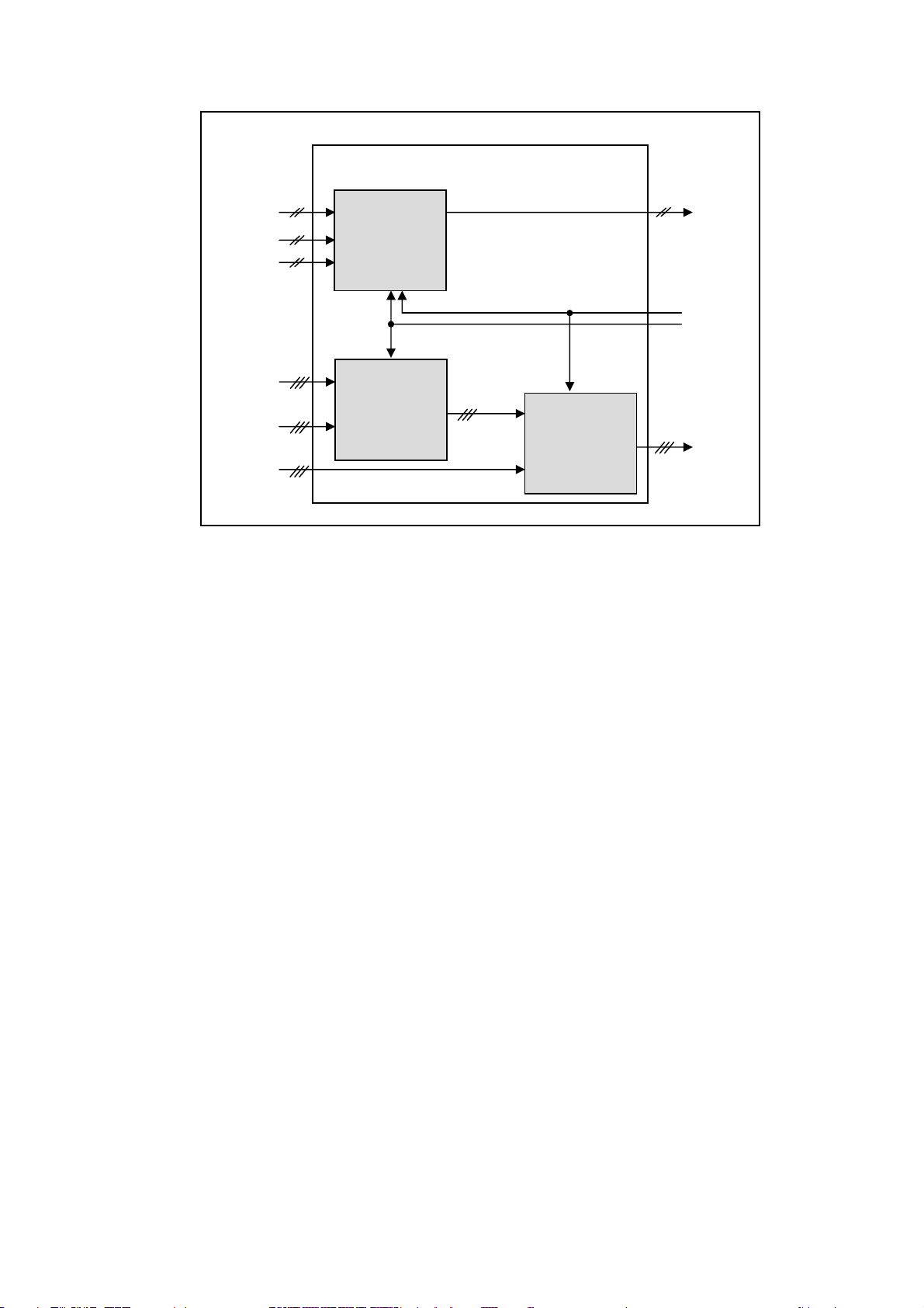
MUX BLOCK
V[R,G,B]IN
YCbCr
[R,G,B]OUT
RGB
TV_[HS,VS]
PC_[HS,VS]
HD_[HS,VS]
MUX
74HC4052D
VIDEO
SWITCH
P15V330
Figure 1: MUX Block.
TV_[R,G,B]AIN
VIDEO
SWITCH
P15V330
AHSYNC
AVSYNC
Control Signals:
VGA_TV_SW
YUV_TV_SW
77
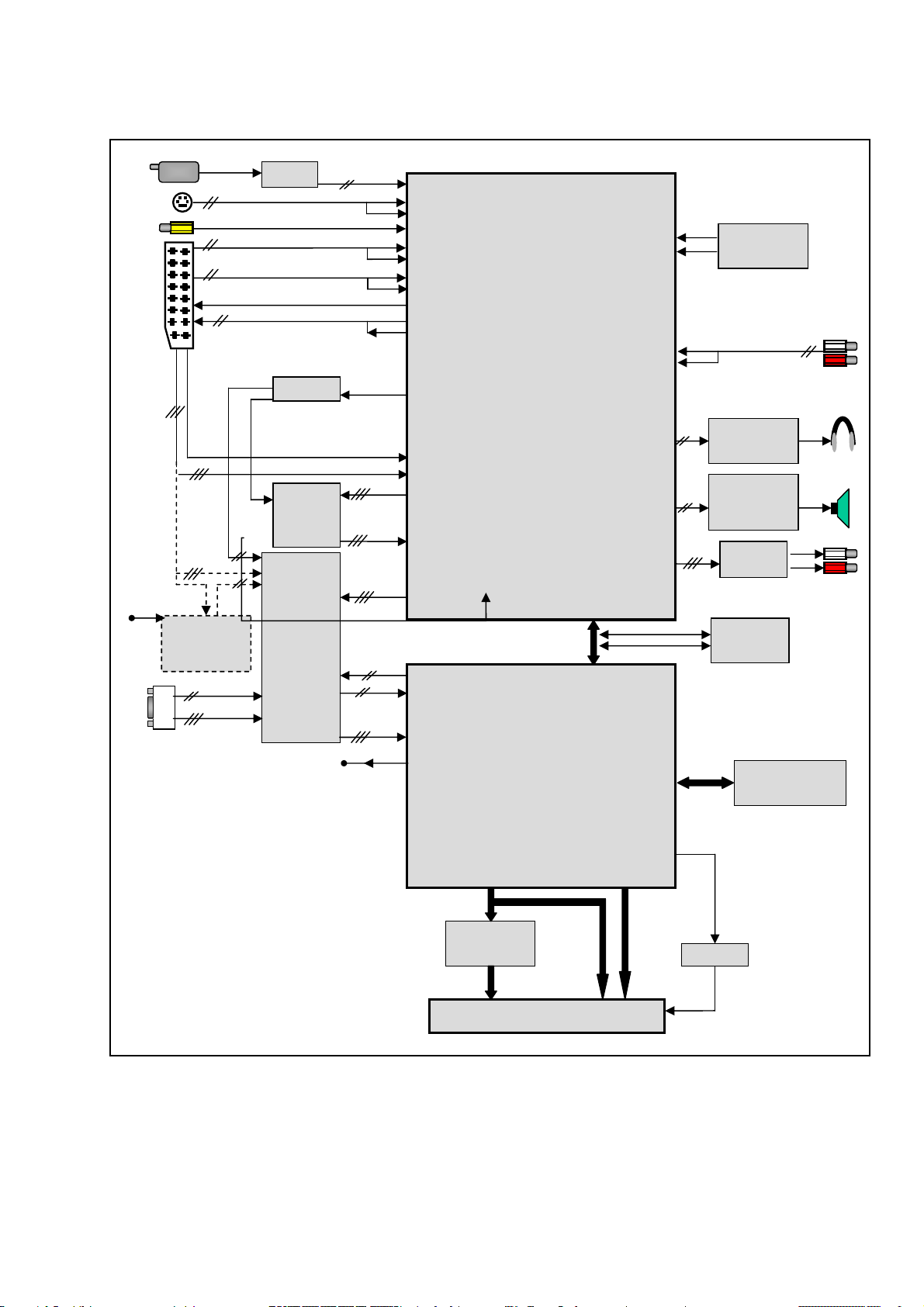
SAW
RF in
MACROVISION
S-Video in
CVBS in
Scart
TV_HS
TV_VS
VFIN (24,25)
UOCIII
Y4(51)
C4(52)
CVBS3/Y3(58) IDTV RGB(70,71,72)
AUDIOIN5L(34) IDTV R/L(54,55)
AUDIOIN5R(35)
C2(59)
CVBS2/Y2(55)
IFVO(43)
AUDIOUTSL(36)
AUDIOUTSR(37)
AUDIOIN3L(56)
AUDIOIN3R(57)
VDRA,HOUT(23,67)
16MB39
IDTV Module
Audio in
[R,G,B]IN
PC in
Y HD_[HS,VS]
SYNC
SEPARATOR
EL1883
PC_[HS,VS]
CTI/
LTI
MUX
BLOCK
[YUV,VGA]_SW
A[H,V]SYNC
FBLIN
AUDOUTHP[L,R](62,63)
R,G,B(78,79,80)
[Y,U,V]OUT(74,75,76)
AUDOUTLS[L,R](60,61)
YUV(72,71,70)
I2SDO2(104)
I2SCLK(103)
I2SWS(102)
[R,G,B]OUT(85,86,87)
Comunication
Signals:
I2C and Handhake
PORTD[5,6](58,57)
[H,V]SYNC(65,64)
SDA_U, SCL_U
PW1306
[R,G,B]AIN(37,43,50)
PORTD7(56)
Communication Interface UART: Rx,Tx, Up-IRQ
D[R,G,B]E[0-7], PORTA7(201)
DHS,DVS,DEN,DCLK D[R,G,B]O[0-7]
HP DRIVER
TDA1308
AUDIO
AMPLIFIER
2xTDA7056
DAC
EEPROM
16MB39 IDTV
Audio
line out
LVDS
DS90C385
Figure 2: TV system block diagram.
88
3.3. Side Board(s)
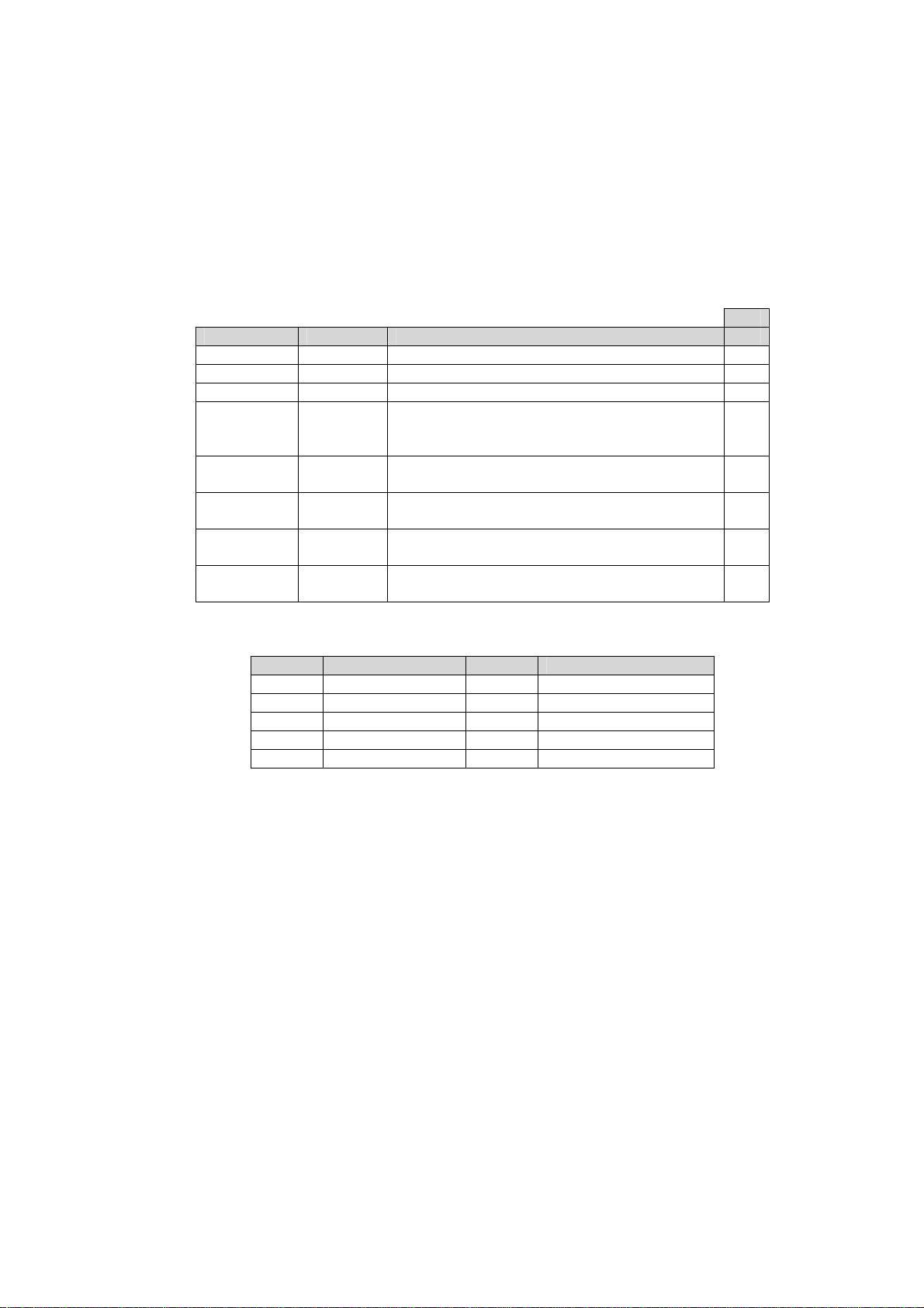
3.3.1.
The keypads (17TK15, 16, 17, 20, 21, 26) for 17MB18 main board are listed in the Table below. (They have the same
connector pinning though):
Connector PL1 on keypads (connected to the connector PL175 on the main board):
Keypads
Key Name Type Function 21
Power Soft sw. Power shut-down and turn on X
Stand-by Tact sw. Switch between stand-by and turn on modes. TV/AV Tact sw. Input source select button. X
Menu Tact sw. Display main menu on the screen. If any menu is
active, display the upper menu. If main menu is
active, turn menu off.
Program- Tact sw. Go to the lower program at any time in TV mode.
In menu mode, go to down menu item.
Program+ Tact sw. Go to the upper program at any time in TV mode.
In menu mode, go to up menu item.
Volume- Tact sw. Decrease the volume level in the volume. In menu
mode, go to left menu item.
Volume+ Tact sw. Increase the volume level in the volume. In menu
mode, go to right menu item.
Pin No: Name Pin No: Name:
1 Volume+ 6 Program+
2 Volume- 7 Program3 Ground 8 Menu
4 Not Connected* 9 TV/AV
5 Ground 10 Stand-by/Shut-down
*Reserved: It can be +5V in the future designs if needed.
X
X
X
X
X
3.3.2.
IR&LED board contains LED indicator(s) to show TV’s status (Red for stand-by, green for normal operation) and one IR
receiver to get remote control instructions. All the IR&LED boards have the same circuit and connector pinning but the
different mechanical structure to fit different cabinets (see the related section for schematics and connector pinning).
IR&Led Board
9
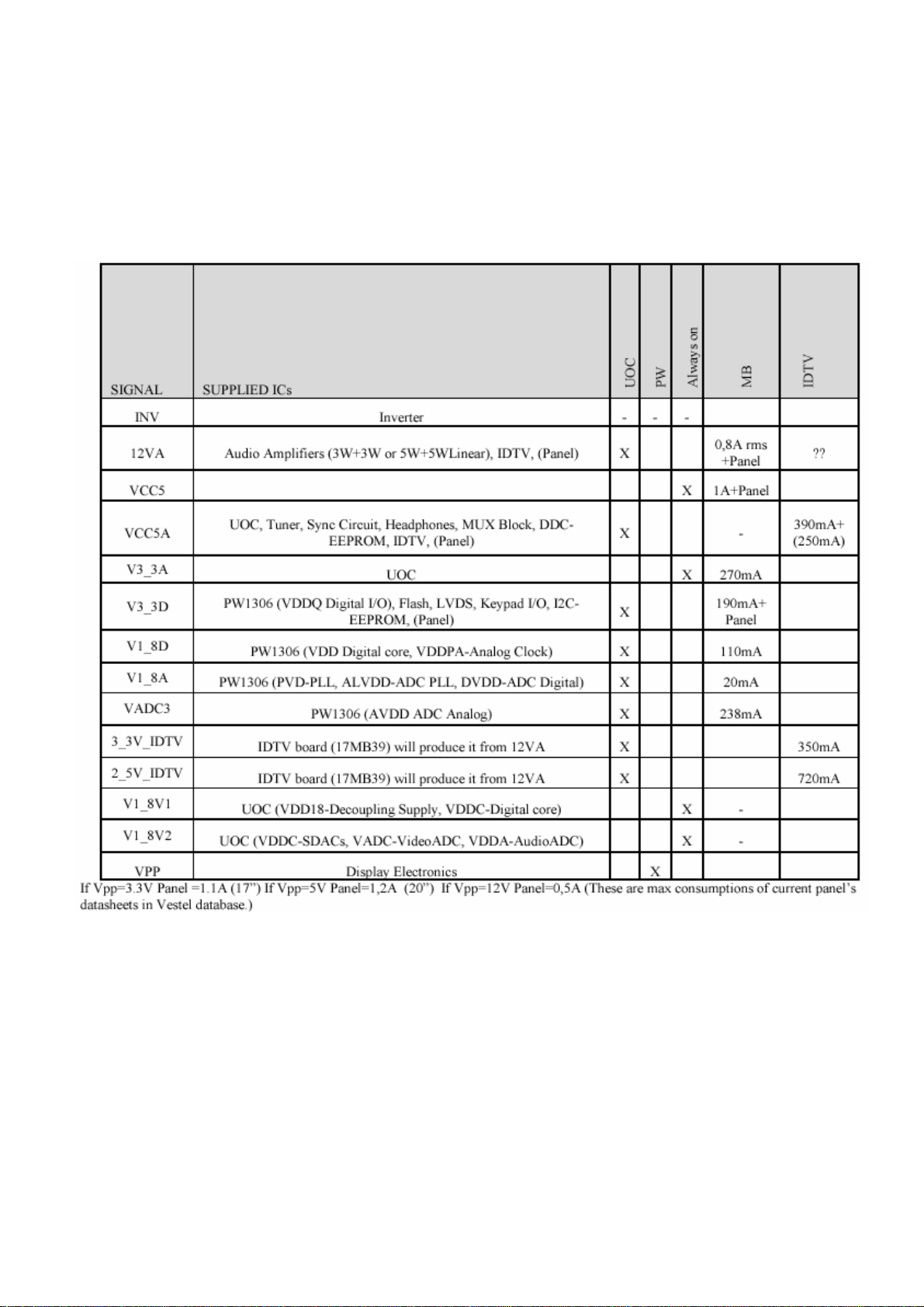
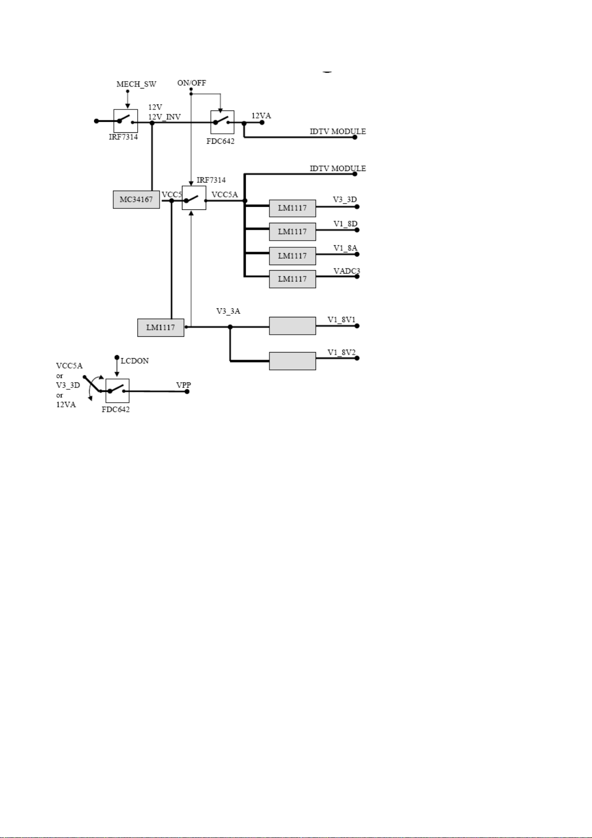
3.4. Power
Several linear regulators and switches are used to generate several separate analog and digital voltage supplies such as +5, +3.3,
+1.8, etc. (Please check the Figure 3, and Table 3 for power management details.)
Table 3: Power management table.
10
11
4. IC AND COMPONENT DESCRIPTIONS
4.1. Basic IC List
No Title Description
IC203 UOCIII Versatile Signal Processor
IC100 PW1306 Video Image Processor with Analog Interface
IC102 MT28F800B3W Flash Memory
IC176 DS90C385 Programmable LVDS Transmitter
IC103 EL1883 Sync Separator
IC405, IC402 P15V330 Wide Bandwidth 2-channel Multiplexer/Demultiplexer
IC404 74HC4052 Dual 4-channel Analog Multiplexer
IC200 TA1366FG LTI/CTI IC
IC410, IC411 TDA7056A Class AB Mono 3W Power Amplifier
IC401 TDA1308 Class AB Stereo Headphone Driver
IC500/1/2/3/4,
LM1117 Linear Regulator
IC201
IC400 24LC21
IC101 24LC32
Serial Electrically Erasable PROM
4.2. UOCIII
The UOCIII series combines the functions of a Video Signal Processor (VSP) together with a FLASH embedded
TEXT/Control/Graphics m-Controller (TCG m-Controller) and US Closed Caption decoder. In addition the following functions
can be added:
Adaptive digital (4H/2H) PAL/NTSC combfilter
Teletext decoder with 10 page text memory
Multi-standard stereo decoder
BTSC stereo decoder
Digital sound processing circuit
Digital video processing circuit
The UOC III series consists of the following 3 basic concepts:
Stereo versions. These versions contain the TV processor with a stereo audio selector, the TCG m-Controller, the multi-
standard stereo or BTSC decoder, the digital sound processing circuit and the digital video processing circuit. Options are
the adaptive digital PAL/NTSC comb filter and a teletext decoder with 10 page text memory.
AV stereo versions. These versions contain the TV processor with stereo audio selector and the TCG m-Controller. Options
are the digital sound processing circuit, the digital video processing circuit, the adaptive digital PAL/NTSC comb filter and
a teletext decoder with a 10 page text memory.
Mono sound versions. These versions contain the TV processor with a selector for mono audio signals and the TCG m-
Controller. Options are the adaptive digital PAL/NTSC combfilter and a teletext decoder with 10 page text memory.
12
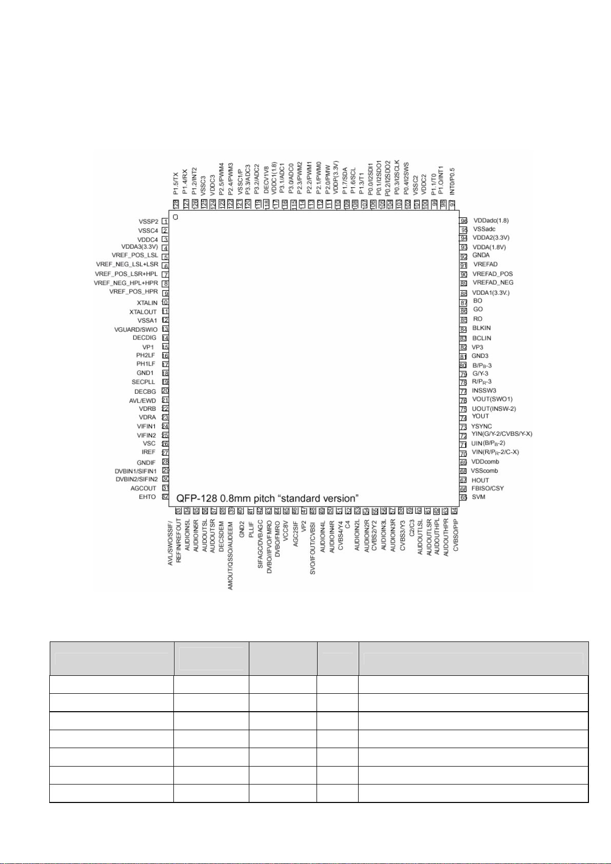
4.2.1. Pinout
Figure 6: UOCIII Pin configuration “stereo” and “AV-stereo” versions with Audio DSP
SYMBOL
VSSP2 1 1 1 ground
VSSC4 2 2 2 ground
VDDC4 3 3 3 digital supply to SDACs (1.8V)
VDDA3(3.3V) 4 4 4 supply (3.3 V)
VREF_POS_LSL 5
VREF_NEG_LSL+HPL 6
VREF_POS_LSR+HPR 7
STEREO +AV
STEREO
AV STEREO
NO AUDIO
DSP
- -
- -
- -
MONO DESCRIPTION
positive reference voltage SDAC (3.3 V)
negative reference voltage SDAC (0 V)
positive reference voltage SDAC (3.3 V)
13
17” TFT TV Service Manual
SYMBOL
STEREO +AV
STEREO
VREF_NEG_HPL+HPR 8
VREF_POS_HPR 9
AV STEREO
NO AUDIO
DSP
- -
- -
MONO DESCRIPTION
negative reference voltage SDAC (0 V)
positive reference voltage SDAC (3.3 V)
XTALIN 10 10 10 crystal oscillator input
XTALOUT 11 11 11 crystal oscillator output
VSSA1 12 12 12 ground
VGUARD/SWIO 13 13 13
V-guard input / I/O switch (e.g. 4 mA current
sinking capability for direct drive of LEDs)
DECDIG 14 14 14 decoupling digital supply
1
VP1 15 15 15
stsupply voltage TV-processor (+5 V)
PH2LF 16 16 16 phase-2 filter
PH1LF 17 17 17 phase-1 filter
GND1 18 18 18 ground 1 for TV-processor
SECPLL 19 19 19 SECAM PLL decoupling
DECBG 20 20 20 bandgap decoupling
EWD/AVL (1)
21 21 21 East-West drive output or AVL capacitor
VDRB 22 22 22 vertical drive B output
VDRA 23 23 23 vertical drive A output
VIFIN1 24 24 24 IF input 1
VIFIN2 25 25 25 IF input 2
VSC 26 26 26 vertical sawtooth capacitor
IREF 27 27 27 reference current input
GNDIF 28 28 28 ground connection for IF amplifier
SIFIN1/DVBIN1 (2)
SIFIN2/DVBIN2 (2)
29 29 29 SIF input 1 / DVB input 1
30 30 30 SIF input 2 / DVB input 2
AGCOUT 31 31 31 tuner AGC output
EHTO 32 32 32 EHT/overvoltage protection input
AVL/SWO/SSIF/
REFO/REFIN
(2)(3)
33 33 33 Automatic Volume Levelling / switch output /
sound IF input / subcarrier reference output /
external reference signal input for I signal mixer for
DVB operation
AUDIOIN5
AUDIOIN5L 34 34
- -
34 audio 5 input
-
audio-5 input (left signal)
AUDIOIN5R 35 35 - audio-5 input (right signal)
AUDOUTSL 36 36
-
audio output for SCART/CINCH (left signal)
AUDOUTSR 37 37 - audio output for SCART/CINCH (right signal)
DECSDEM 38 38 38 decoupling sound demodulator
QSSO/AMOUT/AUDEEM
(2)
39 39 39
QSS intercarrier output / AM output / deemphasis
(front-end audio out)
GND2 40 40 40 ground 2 for TV processor
PLLIF 41 41 41 IF-PLL loop filter
14
AV STEREO
NO AUDIO
DSP
MONO DESCRIPTION
AGC sound IF / internal-external AGC for DVB
applications
Digital Video Broadcast output / IF video output /
FM radio output
SYMBOL
SIFAGC/DVBAGC (2)
DVBO/IFVO/FMRO (2)
STEREO +AV
STEREO
42 42 42
43 43 43
DVBO/FMRO (2) 44 44 - Digital Video Broadcast output / FM radio output
VCC8V 45 45 45 8 Volt supply for audio switches
AGC2SIF 46
VP2 47 47 47
IFVO/SVO/CVBSI (2)
AUDIOIN4
48 48 48
- -
AUDIOIN4L 49 49
- -
AGC capacitor second sound IF
2
ndsupply voltage TV processor (+5 V)
IF video output / selected CVBS output / CVBS
input
49 audio 4 input
-
audio-4 input (left signal)
AUDIOIN4R 50 50 - audio-4 input (right signal)
CVBS4/Y4 51 51 51 CVBS4/Y4 input
C4 52 52 52 chroma-4 input
AUDIOIN2
AUDIOIN2L/SSIF (3)
- -
53 53
53 audio 2 input
-
audio 2 input (left signal) / sound IF input
AUDIOIN2R 54 54 - audio 2 input (right signal)
CVBS2/Y2 55 55 55 CVBS2/Y2 input
AUDIOIN3 - - 56 audio 3 input
AUDIOIN3L 56 56
-
audio 3 input (left signal)
AUDIOIN3R 57 57 - audio 3 input (right signal)
CVBS3/Y3 58 58 58 CVBS3/Y3 input
C2/C3 59 59 59 chroma-2/3 input
AUDOUTLSL 60 62
AUDOUTLSR 61 63
AUDOUT/AMOUT/FMOU
- -
T
-
audio output for audio power amplifier (left signal)
- audio output for audio power amplifier (right
signal)
62
audio output / AM output / FM output, volume
controlled
AUDOUTHPL 62 - - audio output for headphone channel (left signal)
AUDOUTHPR 63
- -
audio output for headphone channel (right signal)
CVBSO/PIP 64 64 64 CVBS / PIP output
SVM 65 65 65 scan velocity modulation output
FBISO/CSY 66 66 66
flyback input/sandcastle output or composite H/V
timing output
HOUT 67 67 67 horizontal output
VSScomb 68 68 68 ground connection for comb filter
VDDcomb 69 69 69 supply voltage for comb filter (5 V)
VIN (R/PRIN2/CX) 70 70 70
UIN (B/PBIN2) 71 71 71
YIN (G/YIN2/CVBS-YX) 72 72 72
V-input for YUV interface (2
C
Xinput)
U-input for YUV interface (2
Y-input for YUV interface (2nd G input / Y input or
CVBS/Y
Xinput))
YSYNC 73 73 73 Y-input for sync separator
15
ndR input / PRinput or
ndB input / PB input)
AV STEREO
NO AUDIO
DSP
MONO DESCRIPTION
SYMBOL
STEREO +AV
STEREO
YOUT 74 74 74 Y-output (for YUV interface)
UOUT (INSSW2) 75 75 75
U-output for YUV interface (2
insertion input)
ndRGB / YPBPR
VOUT (SWO1) 76 76 76 V-output for YUV interface (general purpose
switch output)
3
INSSW3 77 77 77
R/PRIN3 78 78 78
G/YIN3 79 79 79
B/PBIN3 80 80 80
rdRGB / YPBPR insertion input
3
rdR input / PRinput
3
rdG input / Y input
3
rdB input / PBinput
GND3 81 81 81 ground 3 for TV-processor
3
VP3 82 82 82
rdsupply for TV processor
BCLIN 83 83 83 beam current limiter input
BLKIN 84 84 84 black current input
RO 85 85 85 Red output
GO 86 86 86 Green output
BO 87 87 87 Blue output
VDDA1 88 88 88 analog supply for TCG m-Controller and digital
supply for TV-processor (+3.3 V)
VREFAD_NEG 89 89 89 negative reference voltage (0 V)
VREFAD_POS 90 90 90 positive reference voltage (3.3 V)
VREFAD 91
- -
reference voltage for audio ADCs (3.3/2 V)
GNDA 92 92 92 ground
VDDA(1.8V) 93 93 93 analogue supply for audio ADCs (1.8 V)
VDDA2(3.3) 94 94 94 supply voltage SDAC (3.3 V)
VSSadc 95 95 95 ground for video ADC and PLL
VDDadc(1.8) 96 96 96 supply voltage video ADC and PLL
INT0/P0.5 97 97 97
external interrupt 0 or port 0.5 (4 mA current
sinking capability for direct drive of LEDs)
P1.0/INT1 98 98 98 port 1.0 or external interrupt 1
P1.1/T0 99 99 99 port 1.1 or Counter/Timer 0 input
VDDC2 100 100 100 digital supply to core (1.8 V)
VSSC2 101 101 101 ground
P0.4/I2SWS 102
P0.4
-
P0.3/I2SCLK 103
- - port 0.4 or I
102 102 port 0.4
- - port 0.3 or I
2S word select
2S clock
P0.3 - 103 103 port 0.3
P0.2/I2SDO2 104
- - port 0.2 or I
2S digital output 2
P0.2 - 104 104 port 0.2
P0.1/I2SDO1 105
P0.1
-
- - port 0.1 or I
105 105 port 0.1
2S digital output 1
16
SYMBOL
P0.0/I2SDI1/O 106
P0.0
P1.3/T1 107 107 107 port 1.3 or Counter/Timer 1 input
STEREO +AV
STEREO
-
AV STEREO
NO AUDIO
DSP
- - port 0.0 or I
106 106 port 0.0
MONO DESCRIPTION
2S digital input 1 or I2S digital output
P1.6/SCL 108 108 108
P1.7/SDA 109 109 109
VDDP(3.3V) 110 110 110
P2.0/TPWM 111 111 111 port 2.0 or Tuning PWM output
P2.1/PWM0 112 112 112 port 2.1 or PWM0 output
P2.2/PWM1 113 113 113 port 2.2 or PWM1 output
P2.3/PWM2 114 114 114 port 2.3 or PWM2 output
P3.0/ADC0 115 115 115 port 3.0 or ADC0 input
P3.1/ADC1 116 116 116 port 3.1 or ADC1 input
VDDC1 117 117 117 digital supply to core (+1.8 V)
DECV1V8 118 118 118 decoupling 1.8 V supply
P3.2/ADC2 119 119 119 port 3.2 or ADC2 input
P3.3/ADC3 120 120 120 port 3.3 or ADC3 input
VSSC/P 121 121 121 digital ground for m-Controller core and periphery
P2.4/PWM3 122 122 122 port 2.4 or PWM3 output
P2.5/PWM4 123 123 123 port 2.5 or PWM4 output
port 1.6 or I
port 1.7 or I
supply to periphery and on-chip voltage regulator
(3.3 V)
2C-bus clock line
2C-bus data line
VDDC3 124 124 124 digital supply to core (1.8V)
VSSC3 125 125 125 ground
P1.2/INT2 126 126 126 port 1.2 or external interrupt 2
P1.4/RX 127 127 127 port 1.4 or UART bus
P1.5/TX 128 128 128 port 1.5 or UART bus
4.3. PW1306
The PW1306 Video Image Processor is a “system-on-a-chip ” that oversamples and processes RGB or YPbPr video from
analog video decoders. The PW1306 integrates video processing, including deinterlacer and video enhancement filters with a
triple ADC. Analog RGB or YPbPr in PC graphics, standard, or high-definition video can be displayed in either 4:3 or 16:9
formats.
Supports analog video decoders with triple 8-bit Analog-to-Digital Converters (ADCs) up to 140 MSPS conversion rate
Supports Sync-on-Green (SOG), Sync-on-Luma (SOY),and Composite sync inputs
1080i/720p/480p HDTV; 480i and 576i NTSC/PAL SDTV; PC graphics (up to SXGA)
YPbPr/YCbCr/YUV-to-RGB Color Space Converter with programmable coefficients
On-chip, bitmap-based, OSD controller with on-chip memory
24/30/48-bit RGB output with 135 MPixels/second maximum output rate
4.3.1.
Pinout
This section lists the pin functions for the PW1306 208-pin PQFP package. Pin types include:
I/O SR5 (I/O slew rate-controlled,5V input tolerant)
17
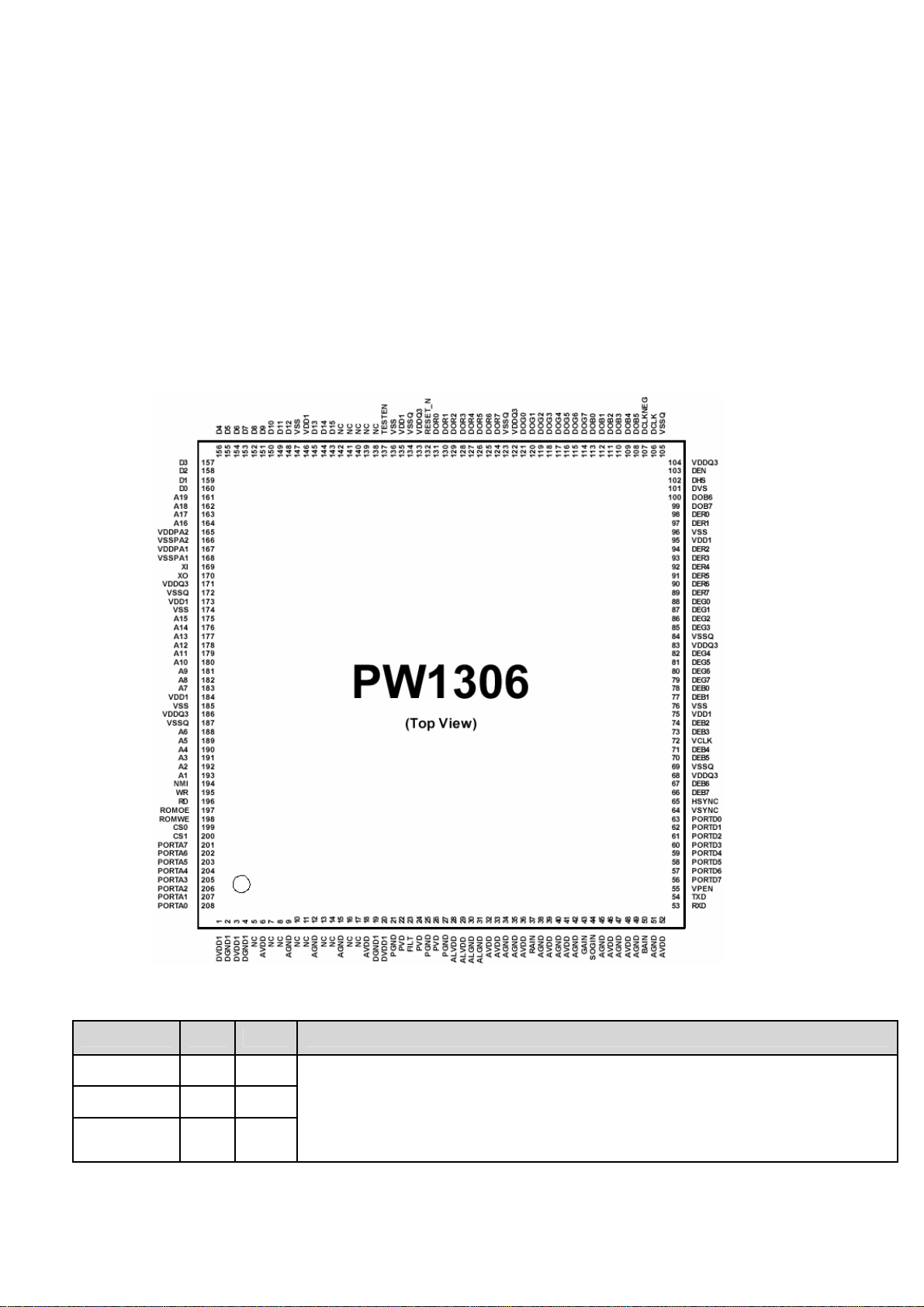
I/O D5 (bidirectional, 5-volt tolerant with pull-down)
I/O U5 (bidirectional, 5-volt tolerant with pull-up)
ID 5 (input, 5-volt tolerant with pull-down)
OS (output with fixed slew-rate control)
AI (analog input, 5-volt tolerant)
DI (digital input, 5-volt tolerant)
DIS (digital input, 5-volt tolerant, Schmitt trigger)
I (XTALIN)
(XTALOUT)
P (power)
NC (no connect)
BOD (bidirectional open drain)
OSR (output with slew rate)
Figure 8: PW1306 Pin configuration.
Signal Pin Type Function
RAIN 37 AI
GAIN 43 AI
BAIN 50 AI
17” TFT TV Service Manual
Red/Green/Blue Analog Inputs. These pins receive the Red, Green and Blue, or
YPbPr/YCbCr/YUV analog signals from the analog video source. For proper
operation of the clamp feature, these inputs must be AC-coupled.
18
Signal Pin Type Function
Analog Sync-On-Green or Sync-On-Luma input. Allows recovery of the HSYNC
SOGIN 44 AI
signal when this pin is AC-coupling to the Green (Red or Blue) analog signal source.
If not used, this pin should be left unconnected.
FILT 23 AI
HSYNC 65 DIS
VSYNC 64 DIS
DCLK 106 OSR
DCLKNEG 107 OSR DPort Pixel Clock.
DVS 101 OS
DHS 102 OS
External PLL Loop Filter. When using the on-chip PLL, this pin must be connected to
an external filter network.
Horizontal Synchronization Input. This digital input signal controls the horizontal scan
frequency by synchronizing the start of the horizontal scan. The logic polarity of this
signal is controlled by the HSPOL bit.
Vertical Synchronization Input. This digital signal controls the vertical scan
frequency.
DPort Pixel Clock. Output clock for the display port pixel data. DCLK is enabled by
the DCLKEN bit and can be inverted by the DCPOL bit. DCLK can be set to run at ½
pixel rate, for dual pixel output mode, by setting the DCK2EN bit. The internal DCLK
clock domain can be disabled by the DCLKOFF bit to reduce power consumption.
DPort Vertical Sync. DVS can be either active-high or active-low depending on the
VSPOL bit. Width and timing is controlled by the VPLSE and VDLY registers.
DPort Vertical Sync. DHS can be either active-high or active-low depending on the
HSPOL bit. Sync width can be controlled by the HPLSE register.
DEN 103 OS
DER0 98 OSR
DER1 97 OSR
DER2 94 OSR
DER3 93 OSR
DER4 92 OSR
DER5 91 OSR
DER6 90 OSR
DER7 89 OSR
DPort Pixel Enable. This signal is active whenever valid data is present. The polarity
is specified by the DENPOL bit.
DEPort Red Pixel Data. In dual pixel output mode these pins are the EVEN red
outputs.
19
 Loading...