

vestel 17MB15 Schematic

27” TFT TV
(17MB15)
SERVICE MANUAL

TABLE OF CONTENTS
1.
INTRODUCTION ...................................................................................................................................... 1
2. TUNER......................................................................................................................................................1
3. IF PART (TDA9886) .................................................................................................................................1
4. MULTI STANDARD SOUND PROCESSOR............................................................................................ 2
5. VIDEO SWITCH TEA6415 ....................................................................................................................... 2
6. AUDIO AMPLIFIER STAGE WITH TPA3002D2 ...................................................................................... 2
7. MICROCONTROLLER ............................................................................................................................. 3
8. EEPROM 24C32....................................................................................................................................... 3
9. CLASS AB STEREO HEADPHONE DRIVER TDA1308 .........................................................................3
10. SAW FILTERS..........................................................................................................................................3
11. IC DESCRIPTIONS .................................................................................................................................. 4
11.1. TEA6415C ......................................................................................................................................... 5
11.1.1. General Description................................................................................................................. 5
11.1.2. Features .................................................................................................................................... 5
11.1.3. Pinning......................................................................................................................................5
11.2. 24LC02 .............................................................................................................................................. 6
11.2.1. Description................................................................................................................................6
11.2.2. Features .................................................................................................................................... 6
11.2.3. Pinning......................................................................................................................................6
11.3. TCET1102G Optocoupler.................................................................................................................. 7
11.3.1. General Description................................................................................................................. 7
11.3.2. General Features......................................................................................................................7
11.3.3. Applications.............................................................................................................................. 8
11.4. SVP-EX 52 ........................................................................................................................................8
11.4.1. General Description................................................................................................................. 8
11.5. TL431 ................................................................................................................................................8
11.5.1. General Description................................................................................................................. 8
11.5.2. Features..................................................................................................................................... 8
11.6. 24C32 ................................................................................................................................................ 8
11.6.1. General Description................................................................................................................. 8
11.6.2. Features .................................................................................................................................... 8
11.6.3. Pinning......................................................................................................................................9
11.7. 74LVC14A .......................................................................................................................................10
11.7.1. Description.............................................................................................................................. 10
11.7.2. Features .................................................................................................................................. 10
11.7.3. Pinning....................................................................................................................................10
11.8. TEA6420.......................................................................................................................................... 11
11.8.1. Features .................................................................................................................................. 11
11.8.2. Description.............................................................................................................................. 11
11.8.3. Pin Connections.....................................................................................................................11
11.9. CS4334............................................................................................................................................ 11
11.9.1. Features .................................................................................................................................. 11
11.9.2. General Description............................................................................................................... 11
11.9.3. Pin Descriptions.....................................................................................................................12
11.10. GAL16LV8 ....................................................................................................................................... 12
11.10.1. Description.............................................................................................................................. 12
11.10.2. Features .................................................................................................................................. 12
11.10.3. Pin connections...................................................................................................................... 13
11.11. K6R4008V1D................................................................................................................................... 13
11.11.1. Description.............................................................................................................................. 13
11.11.2. Features .................................................................................................................................. 13
11.11.3. Pin Description.......................................................................................................................14
11.12. L6562............................................................................................................................................... 14
11.12.1. Features .................................................................................................................................. 14
11.12.2. Description.............................................................................................................................. 14
11.12.3. Pin Connections and Descriptions ...................................................................................... 15
11.13. LM1117............................................................................................................................................ 15
i
TFT TV Service Manual 11/04/2006

11.13.1.
11.13.2. Features .................................................................................................................................. 15
11.13.3. Applications............................................................................................................................ 15
11.13.4. Connection Diagrams............................................................................................................ 16
11.14. LM317.............................................................................................................................................. 16
11.14.1. General Description............................................................................................................... 16
11.14.2. Features .................................................................................................................................. 16
11.14.3. Pin Description.......................................................................................................................16
11.15. LM809.............................................................................................................................................. 16
11.15.1. General Description............................................................................................................... 16
11.15.2. Features .................................................................................................................................. 16
11.15.3. Pinning....................................................................................................................................17
11.16. MSP34X1G...................................................................................................................................... 17
11.16.1. Introduction ............................................................................................................................ 17
11.16.2. Features .................................................................................................................................. 18
11.16.3. Pin connections...................................................................................................................... 18
11.17. M29W040B......................................................................................................................................20
11.17.1. Description.............................................................................................................................. 20
11.17.2. Features .................................................................................................................................. 20
11.17.3. Pin Descriptions.....................................................................................................................21
11.18. MC33202 ......................................................................................................................................... 21
11.18.1. General Description............................................................................................................... 21
11.18.2. Features .................................................................................................................................. 21
11.18.3. Pin Connections.....................................................................................................................21
11.19. PCF8574 .........................................................................................................................................22
11.19.1. General Description............................................................................................................... 22
11.19.2. Features .................................................................................................................................. 22
11.19.3. Pinning....................................................................................................................................22
11.20. PI5V330...........................................................................................................................................23
11.20.1. General Description............................................................................................................... 23
11.21. SDA55XX (SDA5550)......................................................................................................................23
11.21.1. General description ............................................................................................................... 23
11.22. Sil 9993............................................................................................................................................ 23
11.22.1. General Description............................................................................................................... 23
11.22.2. Features .................................................................................................................................. 24
11.23. NCP1014 ......................................................................................................................................... 24
11.23.1. General Description............................................................................................................... 24
11.23.2. Features .................................................................................................................................. 24
11.23.3. Pin Connections and Descriptions ...................................................................................... 25
11.24. SN74CB3Q3305..............................................................................................................................25
11.24.1. General Description............................................................................................................... 25
11.24.2. Features .................................................................................................................................. 25
11.24.3. Pin Connections.....................................................................................................................26
11.25. ST24LC21 .......................................................................................................................................26
11.25.1. Description.............................................................................................................................. 26
11.25.2. Features .................................................................................................................................. 26
11.25.3. Pin connections...................................................................................................................... 26
11.26. LM2576............................................................................................................................................ 27
11.26.1. General Description............................................................................................................... 27
11.26.2. Features .................................................................................................................................. 27
11.26.3. Pin description ....................................................................................................................... 27
11.27. TDA1308 .........................................................................................................................................27
11.27.1. General Description............................................................................................................... 27
11.27.2. Features .................................................................................................................................. 27
11.27.3. Pinning....................................................................................................................................28
11.28. TDA9886 .........................................................................................................................................28
11.28.1. General Description............................................................................................................... 28
11.28.2. Features .................................................................................................................................. 28
11.28.3. Pinning....................................................................................................................................28
11.29. TPA3002D2 ..................................................................................................................................... 29
General Description............................................................................................................... 15
ii
TFT TV Service Manual 11/04/2006

11.29.1.
11.29.2. Features .................................................................................................................................. 29
11.29.3. Pinning....................................................................................................................................30
11.30. µPA672T.......................................................................................................................................... 31
11.30.1. General Description............................................................................................................... 31
11.30.2. Features .................................................................................................................................. 31
11.30.3. Pin Connection....................................................................................................................... 31
11.31. VPC3230D....................................................................................................................................... 31
11.31.1. General Description............................................................................................................... 31
11.31.2. Pin Connections and Short Descriptions............................................................................ 32
12. SERVICE MENU SETTINGS ................................................................................................................. 33
12.1. Picture Adjust ..................................................................................................................................33
12.2. SOUND1.......................................................................................................................................... 34
12.3. SOUND 2......................................................................................................................................... 34
12.4. Options ............................................................................................................................................ 34
12.5. TV Norm ..........................................................................................................................................35
12.6. Features ..........................................................................................................................................35
12.7. Teletext............................................................................................................................................35
12.8. Source ............................................................................................................................................. 35
12.9. Menu Languages 1 & 2 ................................................................................................................... 35
13. BLOCK DIAGRAM....................................................................................................................................1
14. CIRCUIT DIAGRAM .................................................................................................................................1
15. CIRCUIT DIAGRAMS...............................................................................................................................3
General Description............................................................................................................... 29
iii
TFT TV Service Manual 11/04/2006

1. INTRODUCTION
27” TFT TV is a progressive TV control system with built-in de-interlacer and scaler. It uses a
1366*768 panel with 16:9 aspect ratio. The TV is capable of operation in PAL, SECAM, NTSC
(playback) colour standards and multiple transmission standards as B/G, D/K, I/I’, and L/L’ including
German and NICAM stereo. Sound system output is supplying 2x8W (10%THD) for stereo 8
speakers. The chassis is equipped with many inputs and outputs allowing it to be used as a center of a
media system.
It supports following peripherals:
2 SCART sockets
1 AV input (CVBS + Stereo Audio)
1 SVHS input
1 Stereo Headphone input
1 Component input (YPbPr + Stereo Audio)
1 D-Sub 15 PC input
1 HDMI input
1 Stereo audio input for PC
Audio line out is taken from the scart with given scart-to-line out connector
2. TUNER
The tuners used in the design are combined VHF, UHF tuners suitable for CCIR systems B/G, H, L, L’,
I/I’, and D/K. The tuning is available through the digitally controlled I
info on one of the Tuners in use.
General description of UV1316:
The UV1316 tuner belongs to the UV 1300 family of tuners, which are designed to meet a wide range of
applications. It is a combined VHF, UHF tuner suitable for CCIR systems B/G, H, L, L’, I and I’. The low
IF output impedance has been designed for direct drive of a wide variety of SAW filters with sufficient
suppression of triple transient.
Features of UV1316:
1. Member of the UV1300 family small sized UHF/VHF tuners
2. Systems CCIR: B/G, H, L, L’, I and I’; OIRT: D/K
3. Digitally controlled (PLL) tuning via I
4. Off-air channels, S-cable channels and Hyper band
5. World standardised mechanical dimensions and world standard pinning
6. Compact size
7. Complies to “CENELEC EN55020” and “EN55013”
Pinning:
1. Gain control voltage (AGC) : 4.0V, Max: 4.5V
2. Tuning voltage
3. I²C-bus address select : Max: 5.5V
4. I²C-bus serial clock : Min:-0.3V, Max: 5.5V
5. I²C-bus serial data : Min:-0.3V, Max: 5.5V
6. Not connected
7. PLL supply voltage : 5.0V, Min: 4.75V, Max: 5.5V
8. ADC input
9. Tuner supply voltage : 33V, Min: 30V, Max: 35V
10. Symmetrical IF output 1
11. Symmetrical IF output 2
2
C-bus
2
C bus (PLL). Below you will find
3. IF PART (TDA9886)
The TDA9886 is an alignment-free multistandard (PAL, SECAM and NTSC) vision and sound IF signal
PLL. The following figure shows the simplified block diagram of the integrated circuit.
The integrated circuit comprises the following functional blocks:
VIF amplifier, Tuner and VIF-AGC, VIF-AGC detector, Frequency Phase-Locked Loop (FPLL) detector,
VCO and divider, Digital acquisition help and AFC, Video demodulator and amplifier, Sound carrier trap,
SIF amplifier, SIF-AGC detector, Single reference QSS mixer, AM demodulator, FM demodulator and
1
TFT TV Service Manual 11/04/2006
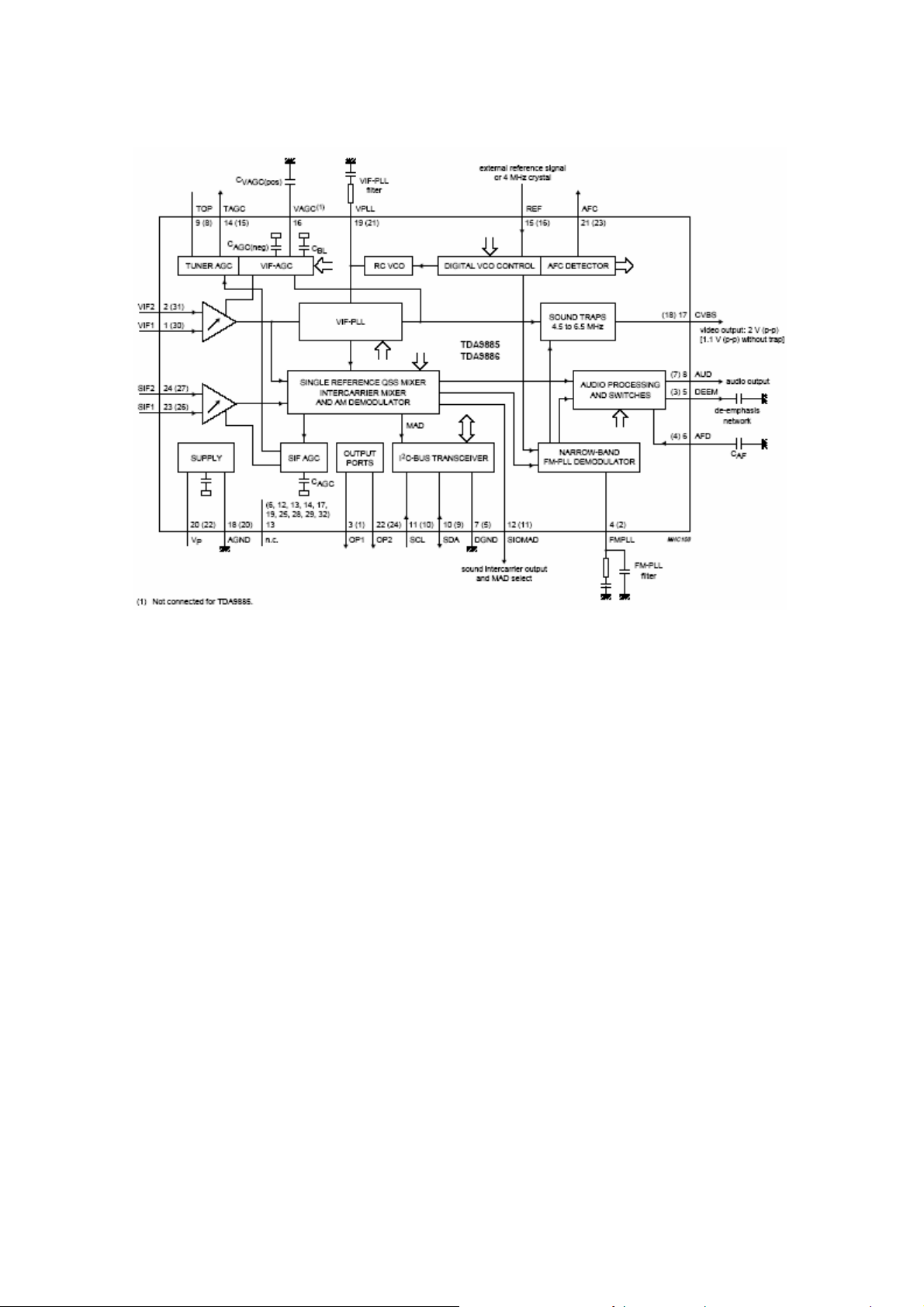
acquisition help, Audio amplifier and mute time constant, I²C-bus transceivers and MAD (module
address), Internal voltage stabilizer
.
4. MULTI STANDARD SOUND PROCESSOR
The MSP34x1G family of single-chip Multistandard Sound Processors covers the sound processing of
all analog TV-Standards worldwide, as well as the NICAM digital sound standards. The full TV sound
processing, starting with analog sound IF signal-in, down to processed analog AF-out, is performed on
a single chip.
These TV sound processing ICs include versions for processing the multichannel television sound
(MTS) signal conforming to the standard recommended by the Broadcast Television Systems
Committee (BTSC). The DBX noise reduction, or alternatively, Micronas Noise Reduction (MNR) is
performed alignment free. Other processed standards are the Japanese FM-FM multiplex standard
(EIA-J) and the FM Stereo Radio standard.
Current ICs have to perform adjustment procedures in order to achieve good stereo separation for
BTSC and EIA-J. The MSP34x1G has optimum stereo performance without any adjustments.
5. VIDEO SWITCH TEA6415
In case of three or more external sources are used, the video switch IC TEA6415 is used. The main
function of this device is to switch 8 video-input sources on the 6 outputs.
Each output can be switched on only one of each input. On each input an alignment of the lowest level
of the signal is made (bottom of sync. top for CVBS or black level for RGB signals).
Each nominal gain between any input and output is 6.5dB.For D2MAC or Chroma signal the alignment
is switched off by forcing, with an external resistor bridge, 5VDC on the input. Each input can be used
as a normal input or as a MAC or Chroma input (with external Resistor Bridge). All the switching
possibilities are changed through the BUS. Driving 75ohm load needs an external resistor. It is possible
to have the same input connected to several outputs.
6. AUDIO AMPLIFIER STAGE WITH TPA3002D2
The TPA3004D2 is a 9-W (per channel) efficient, Class-D audio amplifier for driving bridged-tied stereo
speakers. The TPA3004D2 can drive stereo speakers as low as 8 . The high efficiency of the
TPA3004D2 eliminates the need for external heatsinks when playing music.
Stereo speaker volume is controlled with a dc voltage applied to the volume control terminal offering a
range of gain from –40 dB to 36 dB. Line outputs, for driving external headphone amplifier inputs, are
also dc voltage controlled with a range of gain from –56 dB to 20 dB.
An integrated 5-V regulated supply is provided for powering an external headphone amplifier.
2
TFT TV Service Manual 11/04/2006

7. MICROCONTROLLER
The Micronas SDA 55xx TV microcontroller is dedicated to 8 bit applications for TV control and
provides dedicated graphic features designed for modern low class to mid range TV sets. The SDA
55xx provides also an integrated general purposefully 8051-compatible microcontroller with specific
hardware features especially suitable in TV sets. The microcontroller core has been enhanced to
provide powerful features such as memory banking, data pointers and additional interrupts, etc. The
internal XRAM consists of up to 16 kBytes. The microcontroller provides an internal ROM of up to 128
kBytes. ROMless versions can access up to 1 MByte of external RAM and ROM. The 8-bit
microcontroller runs at 33.33 MHz internal clock. SDA 55xx is realized in 0.25 micron technology with
2.5 V supply voltage for the core and 3.3 V for the I/O port pins to make them TTL compatible. Based
on the SDA 55xx microcontroller the MINTS software package was developed and provides dedicated
device drivers for many Micronas video & audio products and includes a full blown TV control SW for
the PEPER application chassis. The SDA 55xx is also supported with powerful design tools like
emulators from Hitex, Kleinhenz, iSystems, the Keil C51 Compiler and TEDIpro OSD development SW
by Tara Systems.
8. EEPROM 24C32
The Microchip Technology Inc. 24C32 is a 4Kx8 (32 Kbit) Electrically Erasable PROM. This device has
been developed for advanced, low power applications such as personal communications or data
acquisition. The 24C32 features an input cache for fast write loads with a capacity of eight 8-byte
pages, or 64 bytes. It also features a fixed 4K-bit block of ultra-high endurance memory for data that
changes frequently. The 24C32 is capable of both random and sequential reads up to the 32K
boundary. Functional address lines allow up to 8 - 24C32 devices on the same bus, for up to 256K bits
address space. Advanced CMOS technology makes this device ideal for low-power non-volatile code
and data applications.
9. CLASS AB STEREO HEADPHONE DRIVER TDA1308
The TDA1308 is an integrated class AB stereo headphone driver contained in a DIP8 plastic package.
The device is fabricated in a 1 mm CMOS process and has been primarily developed for portable digital
audio applications.
10. SAW FILTERS
K9656M:
Standard:
• B/G
• D/K
• I
• L/L’
Features
• TV IF audio filter with two channels
• Channel 1 (L’) with one pass band for sound carriers at 40.40 MHz (L’) and 39.75 MHz (L’- NICAM)
• Channel 2 (B/G, D/K, L, I) with one pass band for sound carriers between 32.35 MHz and 33.40 MHz
Terminals
• Tinned CuFe alloy
Pin configuration
1 Input
2 Switching input
3 Chip carrier - ground
4 Output
5 Output
K3958M:
Standard:
• B/G
• D/K
• I
• L/L’
3
TFT TV Service Manual 11/04/2006

Features
• TV IF video filter with Nyquist slopes at 33.90 MHz and 38.90 MHz
• Constant group delay
Terminals
Tinned CuFe alloy
Pin configuration
1 Input
2 Input - ground
3 Chip carrier - ground
4 Output
5 Output
11. IC DESCRIPTIONS
TEA6415C
24LC02
4MX32 DDR SDRAM (128M)
TCET1102G OPTOCOUPLER
SVP-EX 52
TL431
24C32
74LVC14A
TEA6420D
CS4334
GAL16LV8
K6R4008V1
L6562D
LM1086
LM1117
LM317T
LM809
MSP3410G
M29W040B
MC33202
PCF8574
PI5V330
SDA5550
SG3525
SII9993
NCP1014
SN74CB3Q3305
ST24LC21
LM2576
MC34063
TDA1308
TDA9886T
TPA3002D2
µPA672T
VPC3230D
4
TFT TV Service Manual 11/04/2006

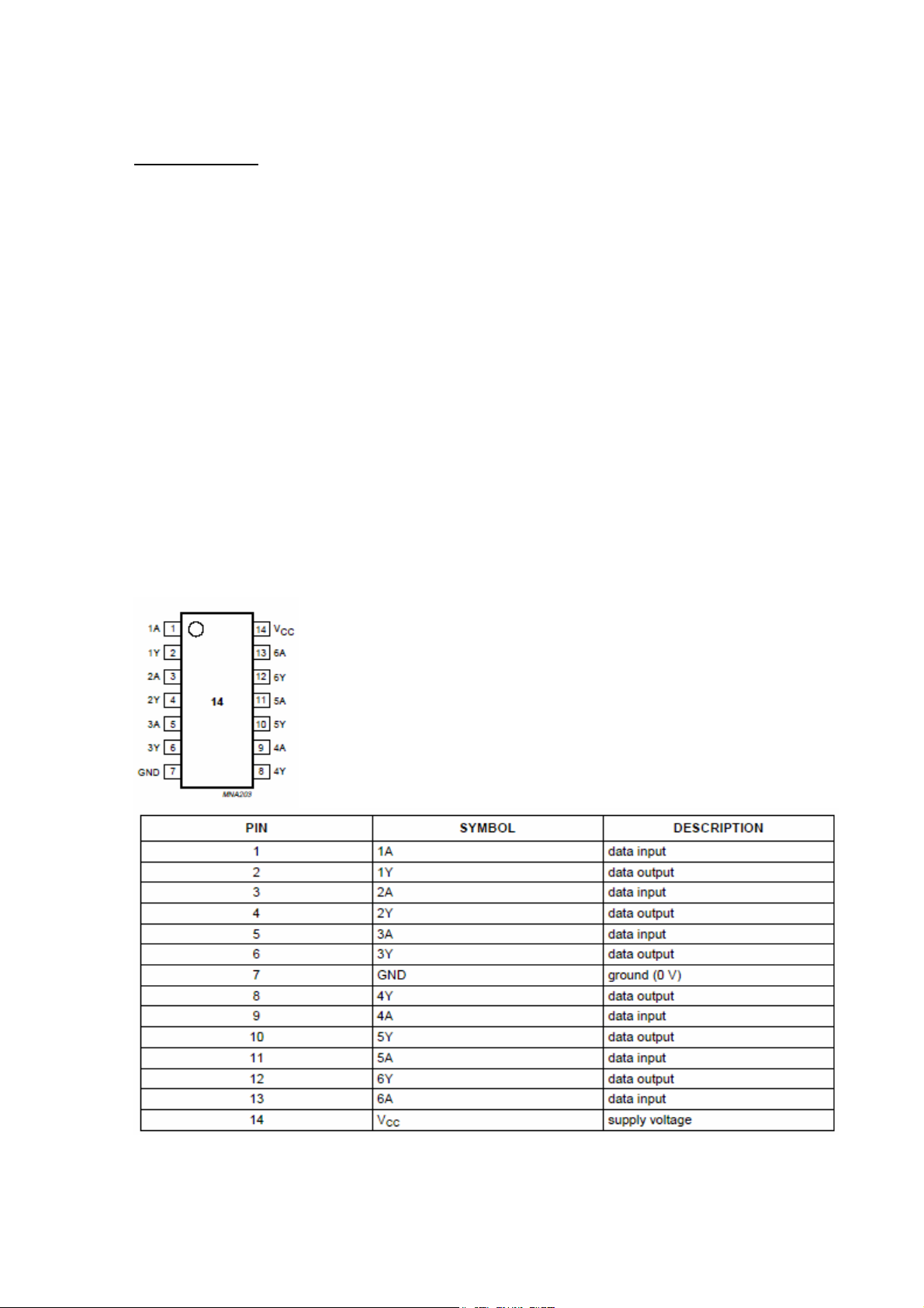
11.1. TEA6415C
11.1.1. General Description
The main function of the IC is to switch 8 video input sources on 6 outputs. Each output can be
switched on only one of each input. On each input an alignment of the lowest level of the signal is made
(bottom of synch. top for CVBS or black level for RGB signals). Each nominal gain between any input
and output is 6.5dB. For D2MAC or Chroma signal the alignment is switched off by forcing, with an
external resistor bridge, 5 V
DC on the input. Each input can be used as a normal input or as a MAC or
Chroma input (with external resistor bridge). All the switching possibilities are changed through the
BUS. Driving 75 load needs an external transistor. It is possible to have the same input connected to
several outputs. The starting configuration upon power on (power supply: 0 to 10V) is undetermined. In
this case, 6 words of 16 bits are necessary to determine one configuration. In other case, 1 word of 16
bits is necessary to determine one configuration.
11.1.2. Features
• 20MHz Bandwidth
• Cascadable with another TEA6415C (Internal address can be changed by pin 7 voltage)
• 8 Inputs (CVBS, RGB, MAC, CHROMA,...)
• 6 Outputs
• Possibility of MAC or chroma signal for each input by switching-off the clamp with an external resistor
bridge
• Bus controlled
• 6.5dB gain between any input and output
• 55dB crosstalk at 5mHz
• Fully ESD protected
11.1.3. Pinning
1. Input : Max : 2Vpp, Input Current: 1mA, Max : 3mA
2. Data : Low level : -0.3V Max: 1.5V,
High level : 3.0V Max : Vcc+0.5V
3. Input : Max : 2Vpp, Input Current: 1mA, Max : 3mA
4. Clock : Low level : -0.3V Max: 1.5V,
High level : 3.0V Max : Vcc+0.5V
5. Input : Max : 2Vpp, Input Current: 1mA, Max : 3mA
6. Input : Max : 2Vpp, Input Current: 1mA, Max : 3mA
7. Prog
8. Input : Max : 2Vpp, Input Current: 1mA, Max: 3mA
9. Vcc : 12V
10. Input : Max : 2Vpp, Input Current: 1mA, Max : 3mA
11. Input : Max : 2Vpp, Input Current: 1mA, Max : 3mA
12. Ground
13. Output : 5.5Vpp, Min : 4.5Vpp
14. Output : 5.5Vpp, Min : 4.5Vpp
15. Output : 5.5Vpp, Min : 4.5Vpp
16. Output : 5.5Vpp, Min : 4.5Vpp
17. Output : 5.5Vpp, Min : 4.5Vpp
18. Output : 5.5Vpp, Min : 4.5Vpp
19. Ground
20. Input : Max : 2Vpp, Input Current : 1mA, Max : 3mA
5
TFT TV Service Manual 11/04/2006
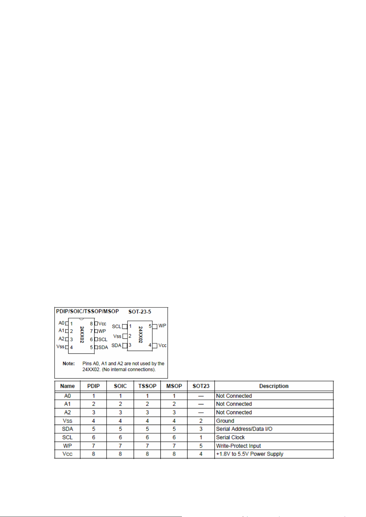
11.2. 24LC02
11.2.1. Description
The Microchip Technology Inc. 24AA02/24LC02B (24XX02*) is a 2 Kbit Electrically Erasable PROM.
The device is organized as one block of 256 x 8-bit memory with a 2-wire serial interface. Low-voltage
design permits operation down to 1.8V, with standby and active currents of only 1µA and 1mA,
respectively. The 24XX02 also has a page write capability for up to 8 bytes of data.
11.2.2. Features
• Single supply with operation down to 1.8V
• Low-power CMOS technology
-1mA active current typical
-1µA standby current typical (I-temp)
• Organized as 1 block of 256 bytes (1 x 256 x 8)
• 2-wire serial interface bus, I
2
C™ compatible
• Schmitt Trigger inputs for noise suppression
• Output slope control to eliminate ground bounce
• 100 kHz (24AA02) and 400 kHz (24LC02B) compatibility
• Self-timed write cycle (including auto-erase)
• Page write buffer for up to 8 bytes
• 2ms typical write cycle time for page write
• Hardware write-protect for entire memory
• Can be operated as a serial ROM
• Factory programming (QTP) available
• ESD protection > 4,000V
• 1,000,000 erase/write cycles
• Data retention > 200 years
• 8-lead PDIP, SOIC, TSSOP and MSOP packages
• 5-lead SOT-23 package
• Pb-free finish available
• Available for extended temperature ranges:
-Industrial (I): -40°C to +85°C
-Automotive (E): -40°C to +125°C
11.2.3. Pinning
6
TFT TV Service Manual 11/04/2006
11.3. TCET1102G Optocoupler
11.3.1. General Description
The TCET110. / TCET2100/ TCET4100 consist of a phototransistor optically coupled to a gallium
arsenide infrared-emitting diode in a 4-lead up to 16-lead plastic dual inline package.
The elements are mounted on one lead frame using a coplanar technique, providing a fixed distance
between input and output for highest safety requirements.
11.3.2. General Features
• CTR offered in 9 groups
• Isolation materials according to UL94-VO
• Pollution degree 2
(DIN/VDE 0110 / resp. IEC 664)
• Climatic classification 55/100/21 (IEC 68 part 1)
• Special construction:
• Therefore, extra low coupling capacity of typical 0.2 pF, high Common Mode Rejection
• Low temperature coefficient of CTR
• G=Leadform10.16mm; provides creepage distance > 8 mm,
for TCET2100/ TCET4100 optional;
• suffix letter 'G' is not marked on the optocoupler
• Coupling System U
7
TFT TV Service Manual 11/04/2006

11.3.3. Applications
Circuits for safe protective separation against electrical shock according to safety class II (reinforced
isolation):
For appl. class I – IV at mains voltage 300 V
For appl. class I – III at mains voltage 600 V
According to VDE 0884, table 2, suitable for: Switch-mode power supplies, line receiver, computer
peripheral interface, microprocessor system interface.
11.4. SVP-EX 52
11.4.1. General Description
SVP EX52 supports two CVBS and one Svideo,two HD YPbPr component or PC RGB input and one
24-bit digital input ports.Supports HD YPbPr de-interlacing mode and 3D-comb video mode.
LVDS "single" port is built-in, supporting output resolution up to SXGA, 1280x1024x60P.
11.5. TL431
11.5.1. General Description
The TL431/TL431Aare three-terminal adjustable regulator series with a guaranteed thermal stability
over applicable temperature ranges. The output voltage may be set to any value between Vref
(approximately 2.5 volts) and 36 volts with two external resistors These devices have a typical dynamic
output impedance of 0.2W Active output circuitry provides a very sharp turn-on characteristic, making
these devices excel lent replacement for zener diodes in many applications.
11.5.2. Features
• Programmable Output Voltage to 36 Volts
• Low Dynamic Output Impedance 0.20 Typical
• Sink Current Capability of 1.0 to 100mA
• Equivalent Full-Range Temperature Coefficient of
50ppm/°C Typical
• Temperature Compensated For Operation Over Full Rated
Operating Temperature Range
• Low Output Noise Voltage
• Fast Turn-on Response
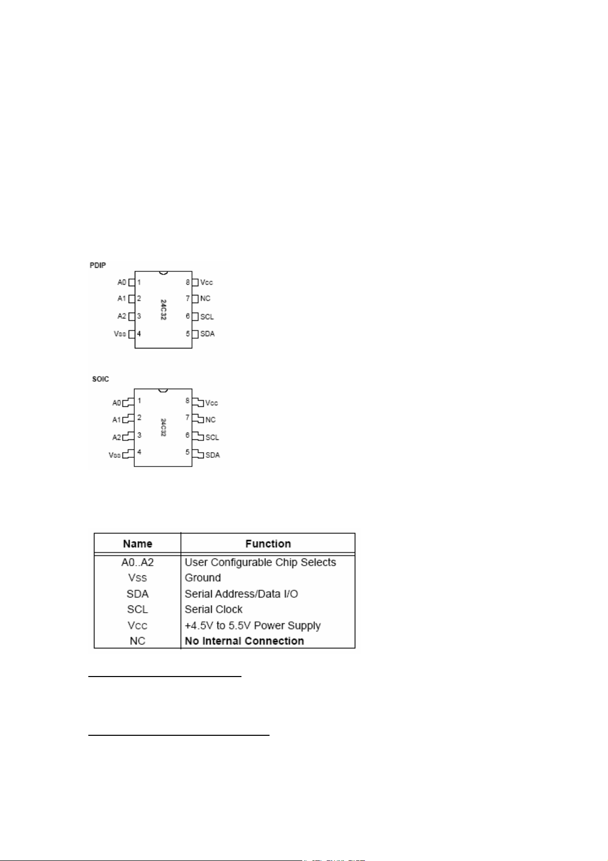
11.6. 24C32
11.6.1. General Description
The Microchip Technology Inc. 24C32 is a 4K x 8 (32K bit) Serial Electrically Erasable PROM. This
device has been developed for advanced, low power applications such as personal communications or
data acquisition. The 24C32 features an input cache for fast write loads with a capacity of eight 8-byte
pages, or 64 bytes. It also features a fixed 4K-bit block of ultra-high endurance memory for data that
changes frequently. The 24C32 is capable of both random and sequential reads up to the 32K
boundary. Functional address lines allow up to 8 - 24C32 devices on the same bus, for up to 256K bits
address space. Advanced CMOS technology makes this device ideal for low-power non-volatile code
and data applications.
11.6.2. Features
• Voltage operating range: 4.5V to 5.5V
- Peak write current 3 mA at 5.5V
- Maximum read current 150µA at 5.5V
- Standby current 1µA typical
• Industry standard two-wire bus protocol, I
2
C™ compatible
-Including 100 kHz and 400 kHz modes
• Self-timed write cycle (including auto-erase)
• Power on/off data protection circuitry
• Endurance:
8
TFT TV Service Manual 11/04/2006
- 10,000,000 Erase/Write cycles guaranteed for High Endurance Block
- 10,000,000 E/W cycles guaranteed for Standard Endurance Block
• 8 byte page, or byte modes available
• 1 page x 8 line input cache (64 bytes) for fast write
loads
• Schmitt trigger, filtered inputs for noise suppression
• Output slope control to eliminate ground bounce
• 2 ms typical write cycle time, byte or page
• Up to 8 chips may be connected to the same bus for up to 256K bits total memory
• Electrostatic discharge protection > 4000V
• Data retention > 200 years
• Temperature ranges:
-Commercial (C): 0°C to +70°C
-Industrial (I): -40°C to +85°C
11.6.3. Pinning
PIN Function Table
PIN DESCRIPTIONS
A0, A1, A2 Chip Address Inputs
The A0...A2 inputs are used by the 24C32 for multiple device operation and conform to the two-wire
bus standard. The levels applied to these pins define the address block occupied by the device in the
address map. A particular device is selected by transmitting the corresponding bits (A2, A1, and A0) in
the control byte.
SDA Serial Address/Data Input/Outpu
t
This is a bidirectional pin used to transfer addresses and data into and data out of the device. It is an
open drain terminal; therefore the SDA bus requires a pull-up resistor to VCC (typical 10KQ for 100
kHz, 1KQ for 400 kHz).
9
TFT TV Service Manual 11/04/2006
For normal data transfer SDA is allowed to change only during SCL low. Changes during SCL high are
reserved for indicating the START and STOP conditions.
SCL Serial Clock
This input is used to synchronize the data transfer from and to the device.
11.7. 74LVC14A
11.7.1. Description
The 74LVC14A is a high-performance, low-power, low-voltage, Si-gate CMOS device, superior to most
advanced CMOS compatible TTL families. Inputs can be driven from either 3.3 or 5V devices. This
feature allows the use of these devices as translators in a mixed 3.3 and 5V environment. The
74LVC14A provides six inverting buffers with Schmitt-trigger action. It is capable of transforming slowly
changing input signals into sharply defined, jitter-free output signals.
11.7.2. Features
• Wide supply voltage range from 1.2 to 3.6 V
• CMOS low power consumption
• Direct interface with TTL levels
• Inputs accept voltages up to 5.5 V
• Complies with JEDEC standard no.8-1A
• ESD protection:
HBM EIA/JESD22-A114-A exceeds 2000V
MM EIA/JESD22-A115-A exceeds 200V.
• Specified from -40 to +85C and -40 to +125C.
11.7.3. Pinning
10
TFT TV Service Manual 11/04/2006
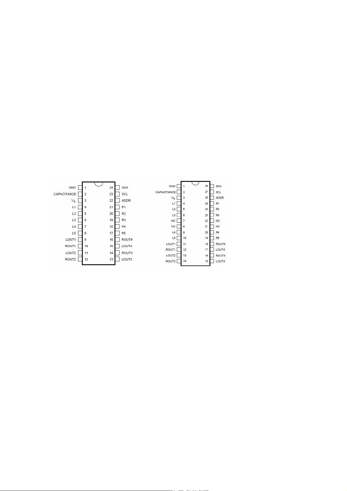
11.8. TEA6420
11.8.1. Features
• 5 Stereo Inputs
• 4 Stereo Outputs
• Gain Control 0/2/4/6dB/Mute for each Output
• Cascadable (2 different addresses)
• Serial Bus Controlled
• Very low Noise
• Very low Distortion
11.8.2. Description
The TEA6420 switches 5 stereo audio inputs on4stereo outputs. All the switching possibilities are
changed through the I
2
C bus.
11.8.3. Pin Connections
11.9. CS4334
11.9.1. Features
• Complete Stereo DAC System: Interpolation, D/A, Output Analog Filtering
• 24-Bit Conversion
• 96 dB Dynamic Range
• -88 dB THD+N
• Low Clock Jitter Sensitivity
• Single +5V Power Supply
• Filtered Line Level Outputs
• On-Chip Digital De-emphasis
• Popgaurd® Technology
• Functionally Compatible with CS4330/31/33
11.9.2. General Description
The CS4334 family members are complete, stereo digital-to-analog output systems including
interpolation, 1-bitD/A conversion and output analog filtering in an 8-pinpackage. The CS4334/5/6/7/8/9
support all major audio data interface formats, and the individual devices differ only in the supported
interface format. The CS4334 family is based on delta-sigma modulation, where the modulator output
controls the reference voltage input to an ultra-linear analog low-pass filter. This architecture allows for
infinite adjustment of sample rate between 2 kHz and 100 kHz simply by changing the master clock
frequency. The CS4334 family contains on-chip digital de-emphasis, operates from a single +5V power
supply, and requires minimal support circuitry. These features are ideal for set-top boxes, DVD players,
SVCD players, and A/V receivers.
11
TFT TV Service Manual 11/04/2006
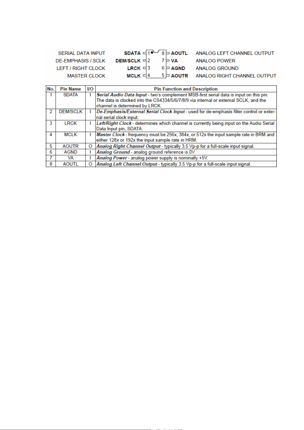
11.9.3. Pin Descriptions
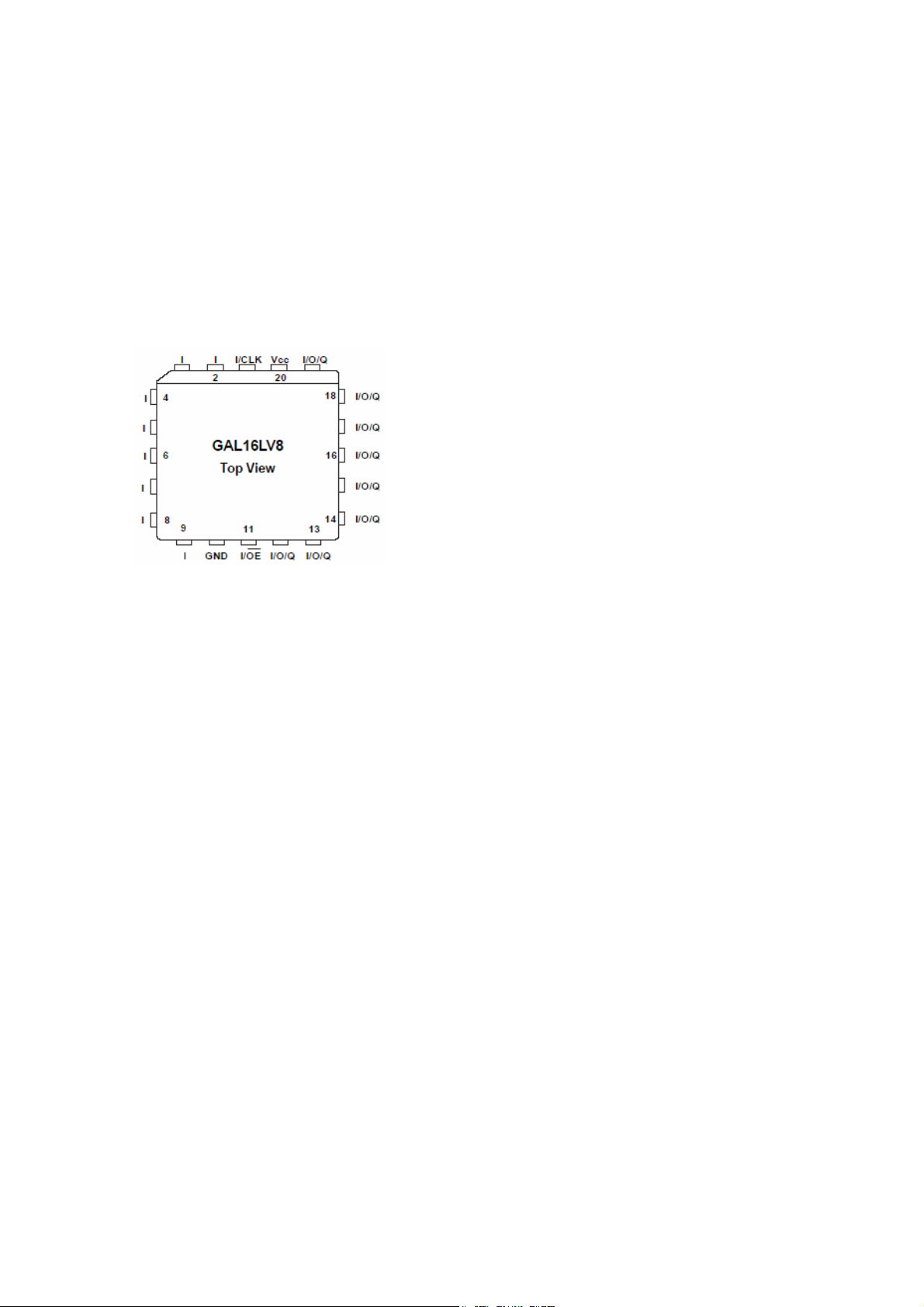
11.10. GAL16LV8
11.10.1. Description
The GAL16LV8D, at 3.5 ns maximum propagation delay time, provides the highest speed performance
available in the PLD market. The GAL16LV8C can interface with both 3.3V and 5Vsignal levels. The
GAL16LV8 is manufactured using Lattice Semiconductor's advanced 3.3V E
combines CMOS with Electrically Erasable (E
2
) floating gate technology. High speed erase times
2
CMOS process, which
(<100ms) allow the devices to be reprogrammed quickly and efficiently.
The 3.3V GAL16LV8 uses the same industry standard 16V8 architecture as its 5V counterpart and
supports all architectural features such as combinatorial or registered macrocell operations.
Unique test circuitry and reprogrammable cells allow complete AC, DC, and functional testing during
manufacture. As a result, Lattice Semiconductor delivers 100% field programmability and functionality
of all GAL products. In addition, 100 erase/write cycles and data retention in excess of 20 years are
specified.
11.10.2. Features
• HIGH PERFORMANCE E2CMOS® TECHNOLOGY
- 3.5 ns Maximum Propagation Delay
- Fmax = 250 MHz
- 2.5 ns Maximum from Clock Input to Data Output
- UltraMOS® Advanced CMOS Technology
• 3.3V LOW VOLTAGE 16V8 ARCHITECTURE
- JEDEC-Compatible 3.3V Interface Standard
- 5V Compatible Inputs
- I/O Interfaces with Standard 5V TTL Devices (GAL16LV8C)
• ACTIVE PULL-UPS ON ALL PINS (GAL16LV8D Only)
• E2 CELL TECHNOLOGY
- Reconfigurable Logic
- Reprogrammable Cells
- 100% Tested/100% Yields
- High Speed Electrical Erasure (<100ms)
- 20 Year Data Retention
• EIGHT OUTPUT LOGIC MACROCELLS
- Maximum Flexibility for Complex Logic Designs
- Programmable Output Polarity
12
TFT TV Service Manual 11/04/2006
• PRELOAD AND POWER-ON RESET OF ALL REGISTERS
- 100% Functional Testability
• APPLICATIONS INCLUDE:
- Glue Logic for 3.3V Systems
- DMA Control
- State Machine Control
- High Speed Graphics Processing
- Standard Logic Speed Upgrade
• ELECTRONIC SIGNATURE FOR IDENTIFICATION
• LEAD-FREE PACKAGE OPTIONS
11.10.3. Pin connections
11.11. K6R4008V1D
11.11.1. Description
The K6R4008V1D is a 4,194,304-bit high-speed Static Random Access Memory organized as 524,288
words by 8 bits. TheK6R4008V1D uses 8 common input and output lines and has an output enable pin
which operates faster than address access time at read cycle. The device is fabricated using
SAMSUNGs advanced CMOS process and designed for high-speed circuit technology. It is particularly
well suited for use in high-density high-speed system applications. The K6R4008V1D is packaged in a
400 mil 36-pin plastic SOJ and 44-pin plastic TSOP type II.
11.11.2. Features
• Fast Access Time 8, 10ns(Max.)
• Low Power Dissipation
- Standby (TTL) : 20mA(Max.)
(CMOS) : 5mA(Max.)
- Operating K6R4008V1D-08 : 80mA(Max.)
K6R4008V1D-10 : 65mA(Max.)
• Single 3.3 ±0.3V Power Supply
• TTL Compatible Inputs and Outputs
• Fully Static Operation
- No Clock or Refresh required
• Three State Outputs
• Center Power/Ground Pin Configuration
• Standard Pin Configuration
K6R4008V1D-J : 36-SOJ-400
K6R4008V1D-K : 36-SOJ-400(Lead-Free)
K6R4008V1D-T : 44-TSOP2-400BF
K6R4008V1D-U : 44-TSOP2-400BF(Lead-Free)
• Operating in Commercial and Industrial Temperature range.
13
TFT TV Service Manual 11/04/2006
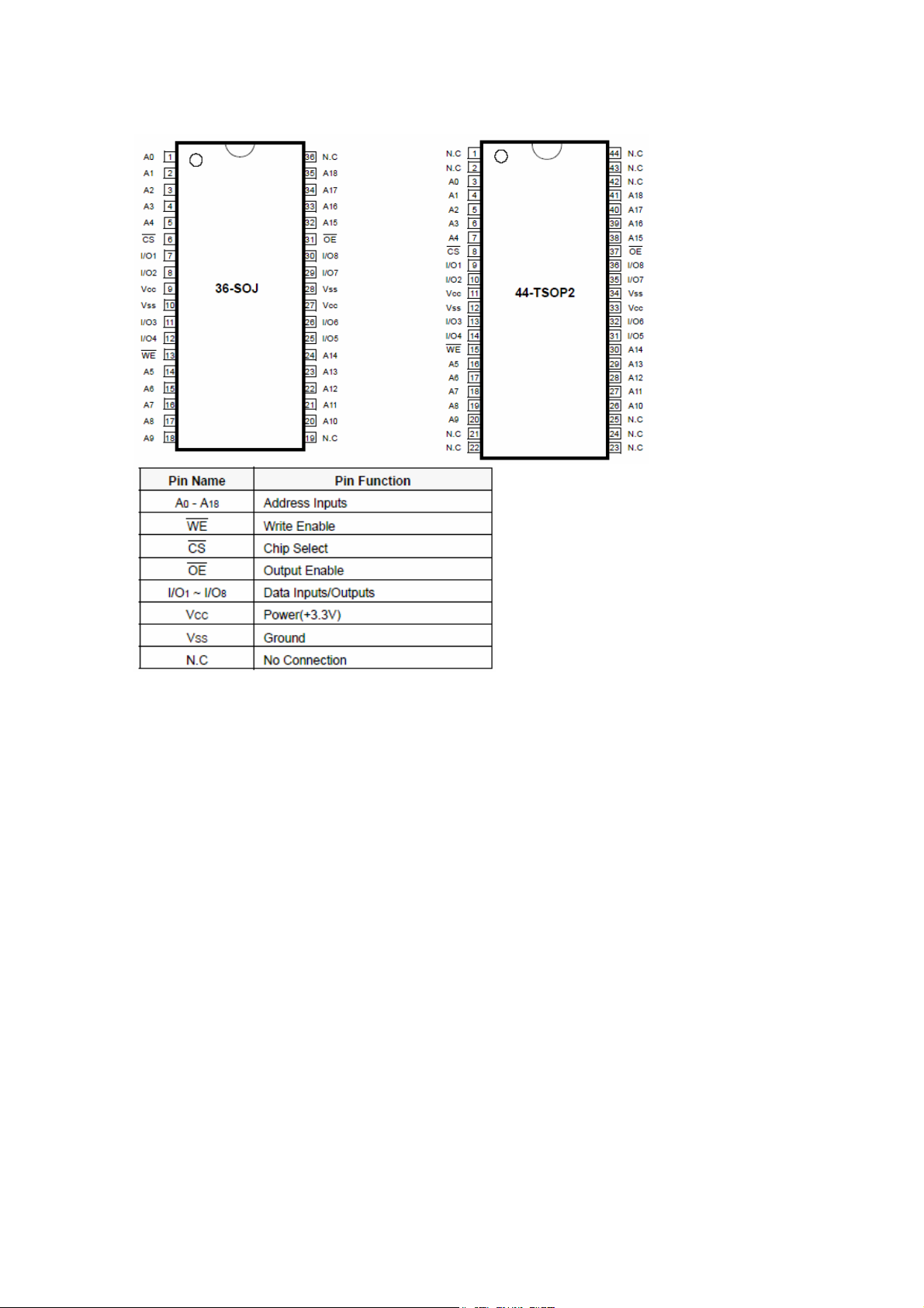
11.11.3. Pin Description
11.12. L6562
11.12.1. Features
• TRANSITION-MODE CONTROL OF PFC PRE-REGULATORS
• PROPRIETARY MULTIPLIER DESIGN FOR MINIMUM THD OF AC INPUT CURRENT
• VERY PRECISE ADJUSTABLE OUTPUT OVERVOLTAGE PROTECTION
• ULTRA-LOW (70µA) START-UP CURRENT
• LOW (4 mA) QUIESCENT CURRENT
• EXTENDED IC SUPPLY VOLTAGE RANGE
• ON-CHIP FILTER ON CURRENT SENSE
• DISABLE FUNCTION
• 1% (@ Tj = 25 °C) INTERNAL REFERENCE VOLTAGE
11.12.2. Description
The L6562 is a current-mode PFC controller operating in Transition Mode (TM). Pin-to-pin compatible
with the predecessor L6561, it offers improved performance. The highly linear multiplier includes a
special circuit, able to reduce AC input current distortion, that allows wide-range-mains operation with
an extremely low THD, even over a large load range.
14
TFT TV Service Manual 11/04/2006
 Loading...