

Page 1

MB110 IDTV
SERVICE MANUAL
Page 2

Table of Contents
1. INTRODUCTION .......................................................................................................................................................... 2
2. T/T2/C/A Tuner (U103) .................................................................................................................................................. 3
3. S/S2 TUNER & DEMODULATOR (U90) OPTIONAL ............................................................................................... 5
4. AUDIO AMPLIFIER STAGES ...................................................................................................................................... 7
A. MAIN AMPLIFIER (U62)(6-8-10 W option) ...................................................................................... ........................... 7
B. MAIN AMPLIFIER (U91)(2.5 W option) .................................................................................................................... 10
C. HEADPHONE AMPLIFIER (U85) ................................................................................................................................ 11
5. POWER STAGE ........................................................................................................................................................... 14
6. MICROCONTROLLER ............................................................................................................................................... 25
A. MSTAR MSD93F3PK2 (U95) ..................................................................................................................................... 25
7. 4Gb DDR3 SDRAM ..................................................................................................................................................... 31
A. Samsung K4B4G1646D (U72) ................................................................................................................................... 31
8. 4Gbit (256M x 8 bit) NAND Flash Memory ................................................................................................................ 32
A. MT29F4G08ABAEAWP (U80) ................................................................................................................................... 32
9. 16M-BIT [16M x 1] CMOS SERIAL FLASH EEPROM ............................................................................................ 34
A. KH25L1606EM2-12G Macronix SPI Flash (U81) ....................................................................................................... 34
10. USB Interface ................................................................................................................................................................ 36
A. CY7C65642 (U73) ..................................................................................................................................................... 36
11. CI Interface ................................................................................................................................................................... 38
12. Software Update ............................................................................................................................................................ 39
A. Main SW update ...................................................................................................................................................... 39
13. Troubleshooting ............................................................................................................................................................ 39
A. No Backlight Problem .............................................................................................................................................. 39
B. CI Module Problem ..........................................................................................................
C. StayIng In Stand-by Mode ........................................................................................................................................ 42
D. IR Problem ................................................................................................................................................................ 43
E. Keypad Touchpad Problems .................................................................................................................................... 43
F. USB Problems ............................................................................................................... ............................................ 44
........................................ 41
G. No Sound Problem ................................................................................................................................................... 44
H. Standby On/Off Problem ......................................................................................................................................... 45
I. No Signal Problem .................................................................................................................................................... 46
14. Service Menu Settings .................................................................................................................................................. 48
15. General Block Diagram ................................................................................................................................................ 53
1
Page 3

1. INTRODUCTION
17MB110 main board is driven by MStar SOC. This IC is a single chip iDTV solution that supports channel
decoding, MPEG decoding, and media-center functionality enabled by a high performance AV CODEC and
CPU.
Key features include:
Combo Front-End Demodulator
A multi standart A/V format decoder
The MACEpro video processor
Home theatre sound processor
Rich internet connectivity and completed digital home network solution
Dual-stream decoder for 3D contents
Mılti-purpose CPU for OS and multimedia
Peripheral and power management
Embedded DRAM
Supported peripherals are:
1 RF input VHF I, VHF III, UHF
1 Satellite input
1 Side AV (CVBS, R/L_Audio)
1 SCART socket(Common)
1 PC input(Common)
3 HDMI input
1 Common interface(Common)
1 Optic/ Coax S/PDIF output
1 Headphone(Common)
2 USB(1x common, 1x optional) and 2x internal USB for Wifi/Bluetooth
1 Ethernet-RJ45
1 External Touchpad/Keyboard/Magic Button
1 DVD(Optional)
2
Page 4

2. T/T2/C/A TUNER (U103)
Description
The Si2151 is Silicon Labs’ sixth-generation hybrid TV tuner supporting all worldwide terrestrial and cable
TV standards. Requiring no external balun, SAW filters, wirewound inductors or LNAs, the Si2151 offers the
lowest-cost BOM for a hybrid TV tuner. Also included are an integrated power-on reset circuit and an option
for single power supply operation. As with prior-generation Silicon Labs TV tuners, the Si2151 maintains very
high linearity and low noise to deliver superior picture quality and a higher number of received stations when
compared to other silicon tuners. The Si2151 offers increased immunity to WiFi and LTE interferance,
eliminating the need for external filtering. For the best performance with next-generation digital TV standards,
such as DVB-T2/C2, the Si2151 delivers industry-leading phase noise performance.
Features
Worldwide hybrid TV tuner
Analog TV: NTSC, PAL/SECAM
Digital TV: ATSC/QAM, DVB-T2/T/C2/C, ISDB-T/C, DTMB
1.7 MHz, 6MHz, 7MHz, 8MHz and 10MHz channel bandwidths
42-1002 MHz frequency range
Industry-leading margin to A/74, NorDig, DTG, ARIB, EN55020, OpenCable™, DTMB
Lowest BOM for a hybrid TV tuner
No balun, SAW filters, or external inductors required
Increased ESD protection on 4pins
Best-in-class real-world reception
Lowest phase noise
High Wi-Fi and LTE immunity
Low power consumption
3.3 V and 1.8 V power supplies
Integrated 1.8 V LDO for 3.3 V single-supply operation
Integrated power-on reset circuit
Standard CMOS process
3x3 mm, 24-pin QFN package
RoHS compliant
3
Page 5
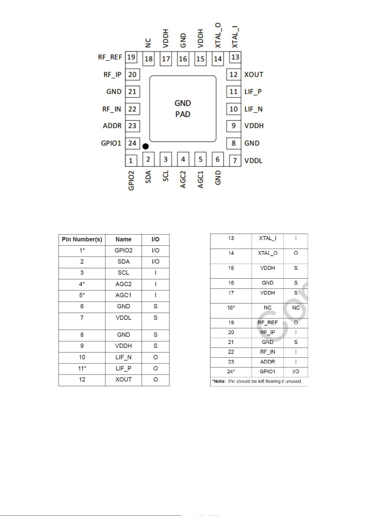
Figure: Pin description
4
Table: Pin functions
Page 6
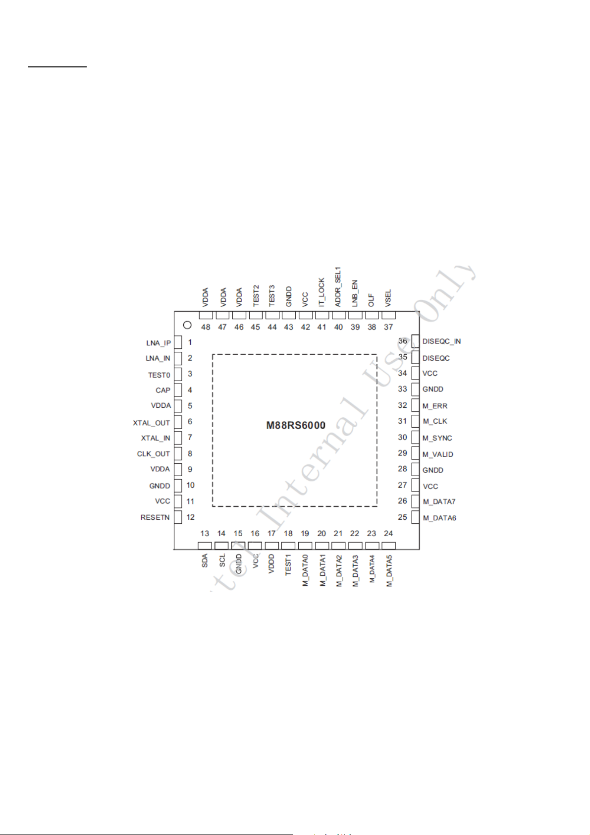
3. S/S2 TUNER & DEMODULATOR (U90) OPTIONAL
Description
The M88RS6000 is highly single-Chip DVB-S2/S receiver. The device is consisting of tuner, a demodulator
and an LNB controller. It is fully compliant with the DVB-S2 and DVB-S standards by supporting QPSK,
(PSK, 16APSK and 32APSK demodulator schemes.)
The tuner is the device an RF signal in the frequency range from 950 MHz to 2150 MHz and down-convert
the signal directly to analog baseband signal, which will be converted to a digital signal in the advanced ADC.
After the ADC, the digital signal will be demodulated in the demodulator, related errors generated during
transmission will be corrected at this stage and finally an MPEG transport stream will be delivered in serial,
parallel or DVB-CI format.
5
Figure: Pin description
Page 7
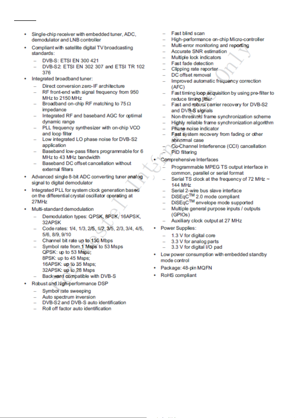
Features
6
Page 8

4. AUDIO AMPLIFIER STAGES
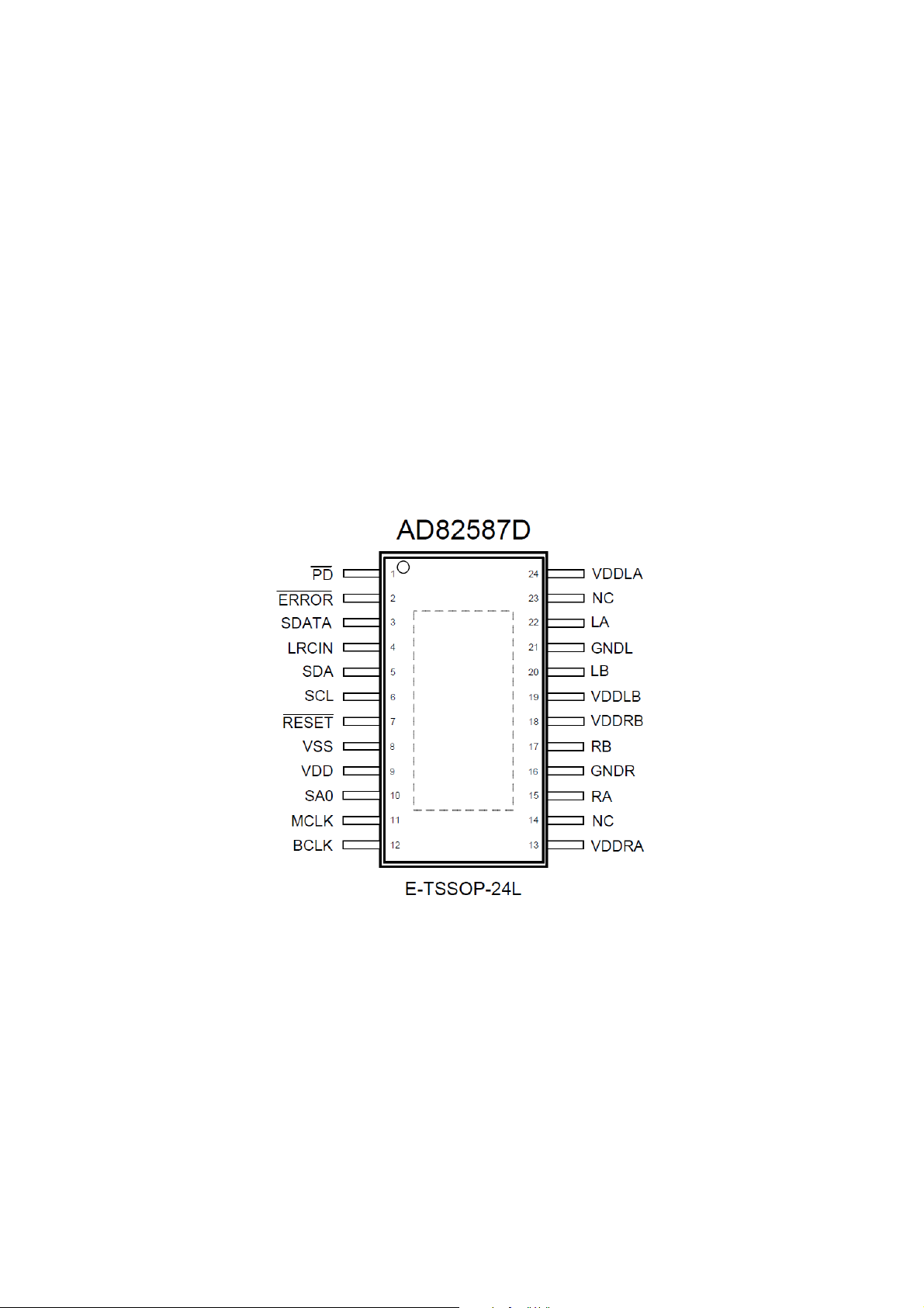
A. MAIN AMPLIFIER (U62)(6-8-10 W OPTION)
Description
AD82587D is a digital audio amplifier capable of driving a pair of 8 ohm, 20W or a single 4ohm, 40W
speaker, both which operate with play music at a 24V supply without external heat-sink or fan requirement.
Using I2C digital control interface, the user can control AD82587D’s input format selection, mute and
volume control functions. AD82587D has many built-in protection circuits to safeguard AD82587D from
connection errors.
Features
16/18/20/24-bit input with I
PSNR & DR(A-weighting) Loudspeaker: 97dB (PSNR), 105dB (DR) @ 24V
Multiple sampling frequencies (Fs)
2
S, Left-alignment and Right-alignment data format
o 32kHz / 44.1kHz / 48kHz and
o 64kHz / 88.2kHz / 96kHz and
o 128kHz/176.4kHz/192kHz
System clock = 64x, 128x, 256x, 384x, 512x, 768x,1024x Fs
o 256x~1024x Fs for 32kHz / 44.1kHz / 48kHz
o 128x~512x Fs for 64kHz / 88.2kHz / 96kHz
o 64x~256x Fs for 128kHz /176.4kHz/192kHz
Supply voltage
o 3.3V for digital circuit
o 10V~26V for loudspeaker driver
Loudspeaker output power for Stereo@ 24V
o 10W x 2ch into 8_ @ 0.16% THD+N
o 15W x 2ch into 8_ @ 0.18% THD+N
o 20W x 2ch into 8_ @ 0.24% THD+N
Loudspeaker output power for Mono@ 24V
o 20W x 1ch into 4_ @ 0.17% THD+N
o 30W x 1ch into 4_ @ 0.2% THD+N
o 40W x 1ch into 4_ @ 0.24% THD+N
Sounds processing including:
o Volume control (+24dB~-103dB, 0.125dB/step)
o Dynamic range control
7
Page 9
o Power clipping
o Channel mixing
o User programmed noise gate with hysteresis window
o DC-blocking high-pass filter
Anti-pop design
Short circuit and over-temperature protection
I2C control interface with selectable device address
Internal PLL
LV Under-voltage shutdown and HV Under-voltage
detection
Power saving mode
Dynamic temperature control
8
Figure: Pin description
Page 10
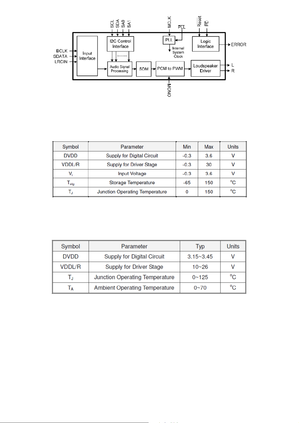
Figure: Functional Block Diagram
Table: Absolute Maximum Ratings
9
Table: Recommended Operating Conditions
Page 11

B. MAIN AMPLIFIER (U91)(2.5 W OPTION)
Description
The AD52010 is a 3.0W stereo, filter-less class-D audio amplifier. Operating with 5.0V loudspeaker driver
supply, it can deliver 3.0W output power into 4 ohm loudspeaker within 10% THD+N or 2.6W at 1% THD+N.
The AD52010 is a stereo audio amplifier with high efficiency and suitable for the notebook computer, and
portable multimedia device.
Features
Supply voltage range: 2.5 V to 5.5 V
Support single-ended or differential analog input
Low Quiescent Current
Low Output Noise
Low shut-down current
Short power-on transient time
Internal pull-low resistor on shut-down pins
Short-circuit protection
Over-temperature protection
Loudspeaker power within 10% THD+N
o 1.78W/ch into 8 ohm loudspeaker
o >3W/ch into 4 ohm loudspeaker
Loudspeaker efficiency
o 93% @ 8 ohm, THD+N=10%
o 85% @ 4 ohm, THD+N=10%
E-TSSOP-14L package
Integrated Feedback Resistor of 300kW
10
Figure: Pin description
Page 12

Table:Pin functions
Table: Recommended operating conditions
C. HEADPHONE AMPLIFIER (U85)
Description
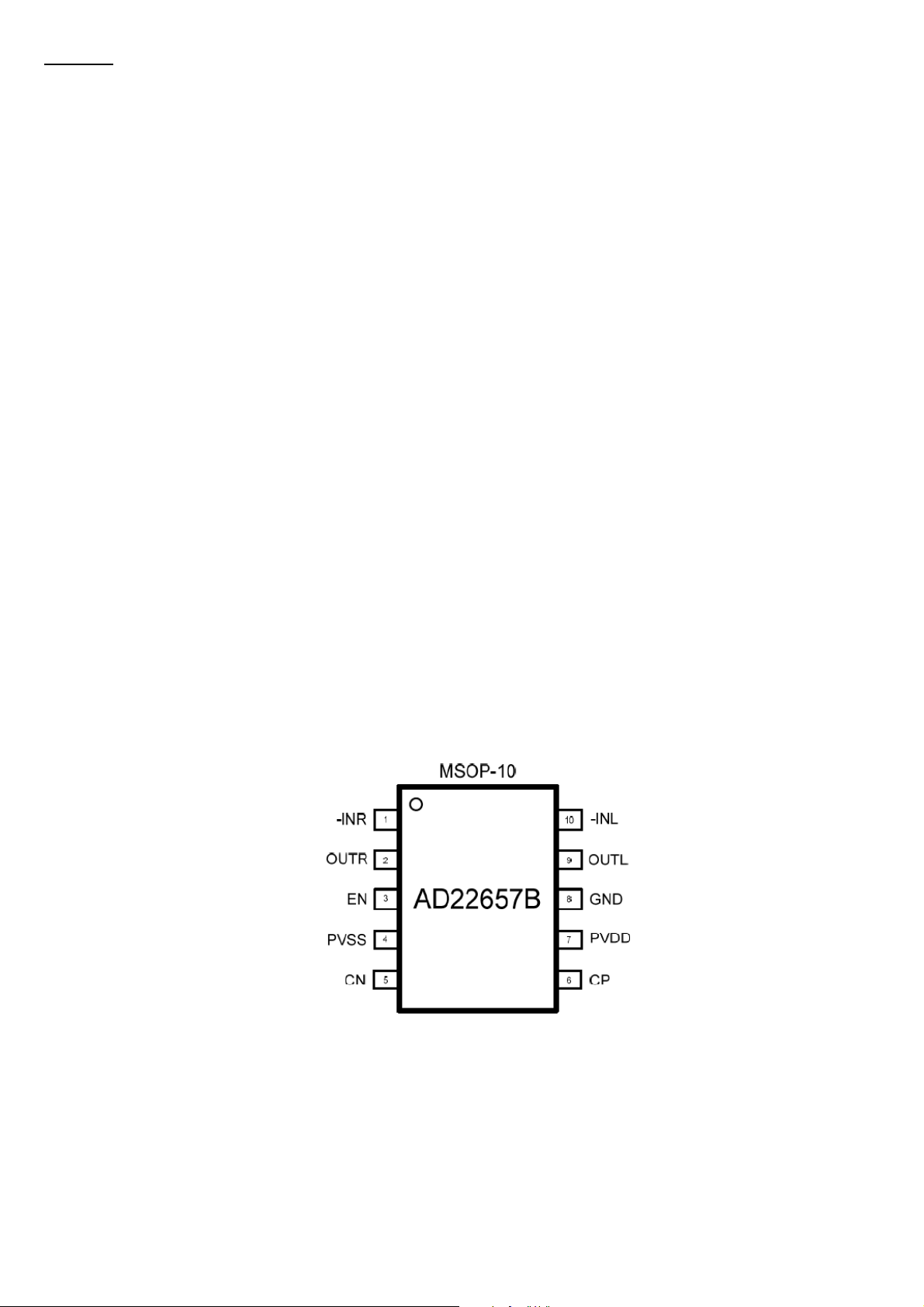
The AD22657B is a 2-Vrms cap-less stereo line driver. The device is ideal for single supply electronics.
Cap-less design can eliminate output dc-blocking capacitors for better low frequency response and save cost.
The AD22657B is capable of delivering 2-Vrms output into a 10k ohm load with 3.3V supply. The gain
settings can be set by users from 1V/V to 10V/V externally. The AD22657B has under voltage protection to
prevent POP noise. Build-in shutdown control and de-pop control sequence also help AD22657B to be a pop-
less device.
The AD22657B is available in a 10-pin MSOP package.
11
Page 13
Features
Operation Voltage: 3V to 3.6V
Cap-less Output
o Eliminates Output Capacitors
o Improves Low Frequency Response
o Reduces POP/Clicks
Low Noise and THD
o Typical SNR 107dB
o Typical Vn 7uVrms
o Typical THD+N < 0.02%
Maximum Output Voltage Swing into 2.5k Load
o 2Vrms at 3.3V Supply Voltage
Single-ended Input
External Gain Setting from 1V/V to 10V/V
Fast Start-up Time: 0.5ms
Integrated De-Pop Control
External Under Voltage Protection
Thermal Protection
Less External Components Required
+/-8kV IEC ESD Protection at line outputs
12
Figure: Pin description
Page 14
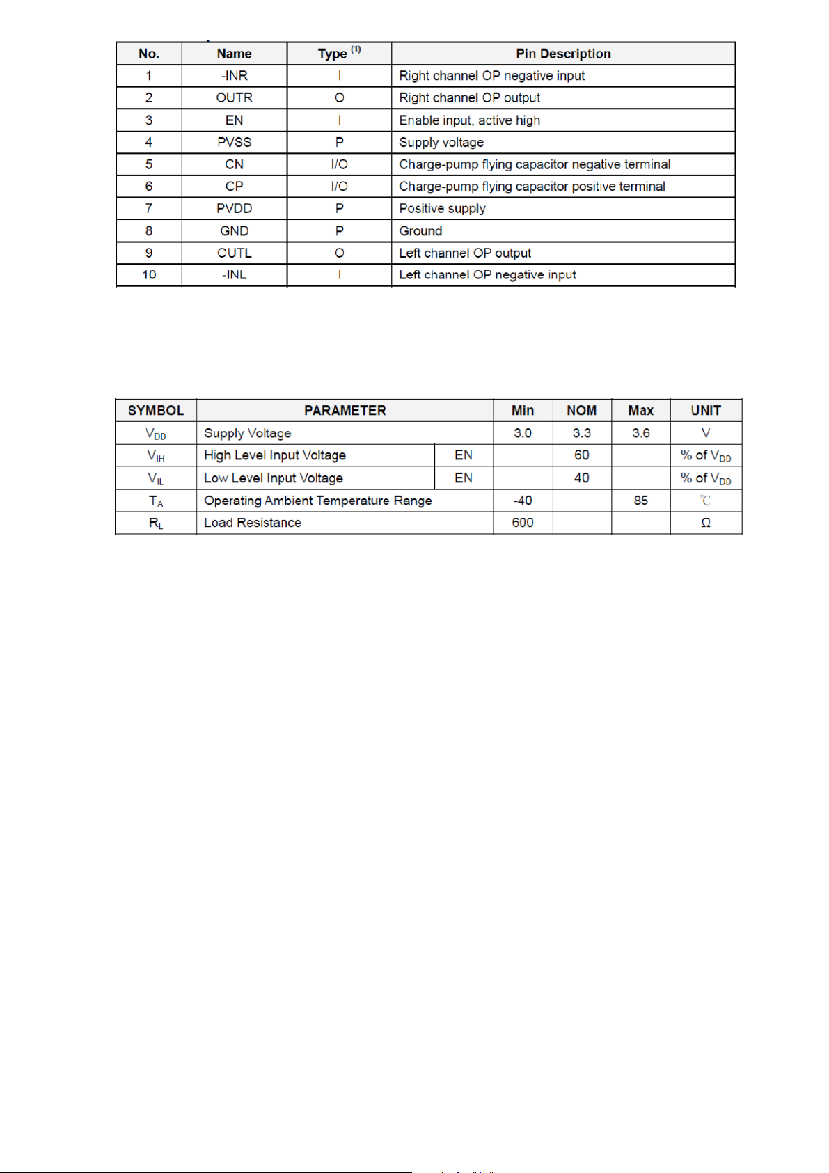
Table: Pin functions
Table: Recommended operating conditions
13
Page 15
5. POWER STAGE
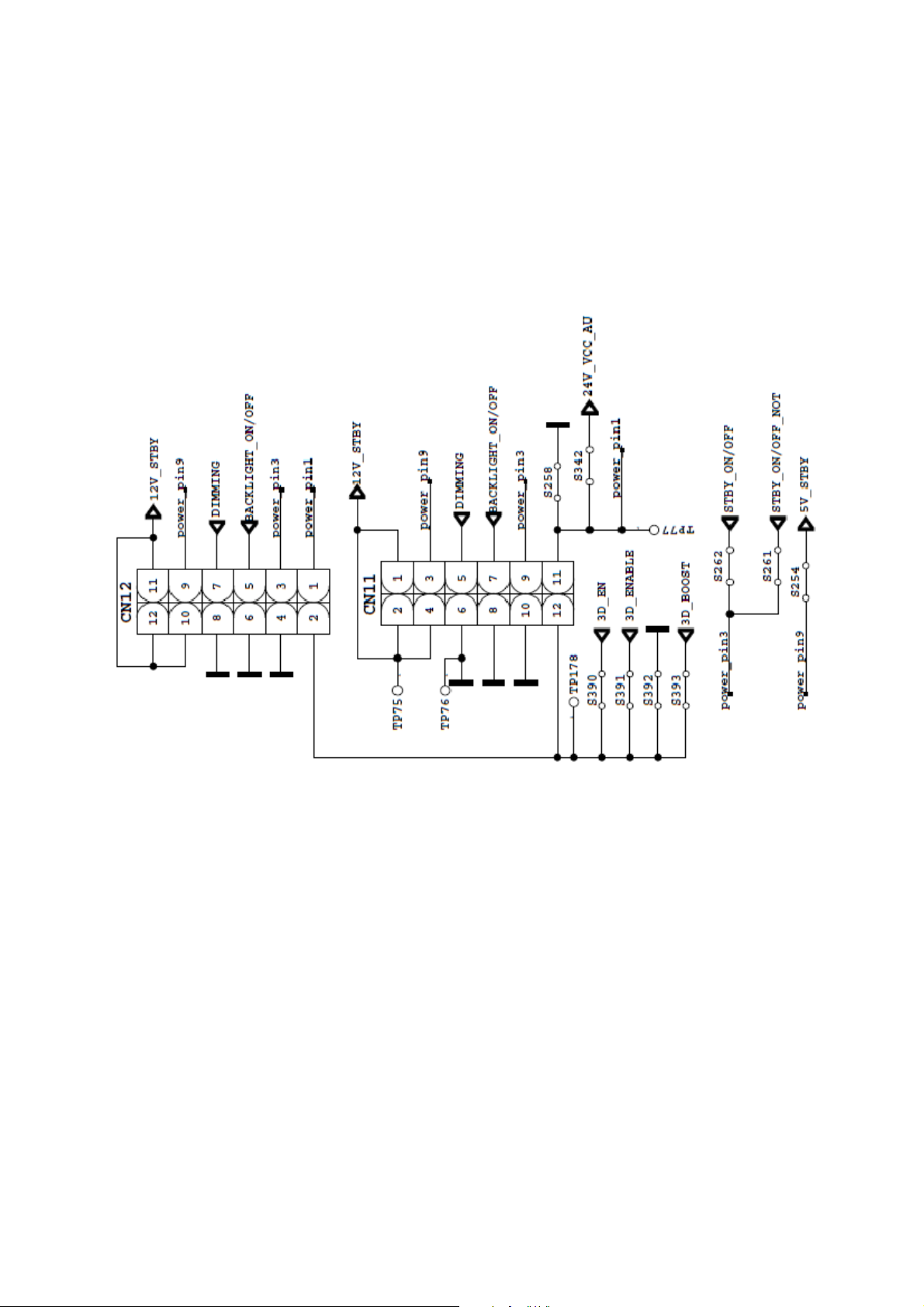
Power socket is used for taking voltages which are 12V_stby and 24V (VDD_Audio for 10W option). These
voltages are produced in power card. Also socket is used for giving dimming, backlight and stand-by signals
with power card. It is shown in figure.
14
Figure: Power socket and power options
Page 16

List of the components are:
SW1(Q56) → NTGS3446
SW2(Q44) → FDC642P
STP1(U63) → RT7278G(12V panel option)
STP1(U63) → TPS54528(5V panel option)
STP2(U102) → TPS54528
STP3(U70) → TPS54329
STP4(U100) → RT6213
LDO1(U94) → LM1117
LDO3(U89) → APL5910
LDO4(U65) → APL5910
15
Page 17

FDC642P
Description and Features
NGTS3446
Features
Ultra Low RDS(ON)
Higher Efficiency Extending Battery Life
Logic Level Gate Drive
Diode Exhibits High Speed, Soft Recovery
Avalanche Energy Specified
IDSS Specified at Elevated Temperature
Pb−Free Package is Available
Figure: Pin description
16
Page 18
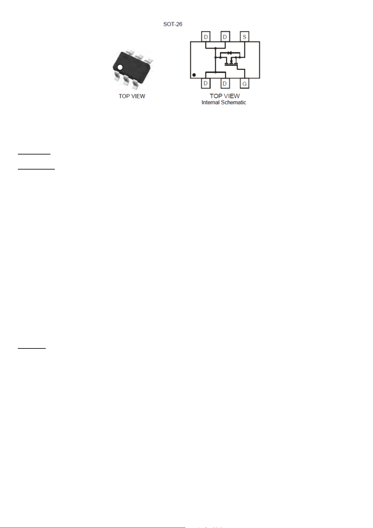
Figure: Pin description
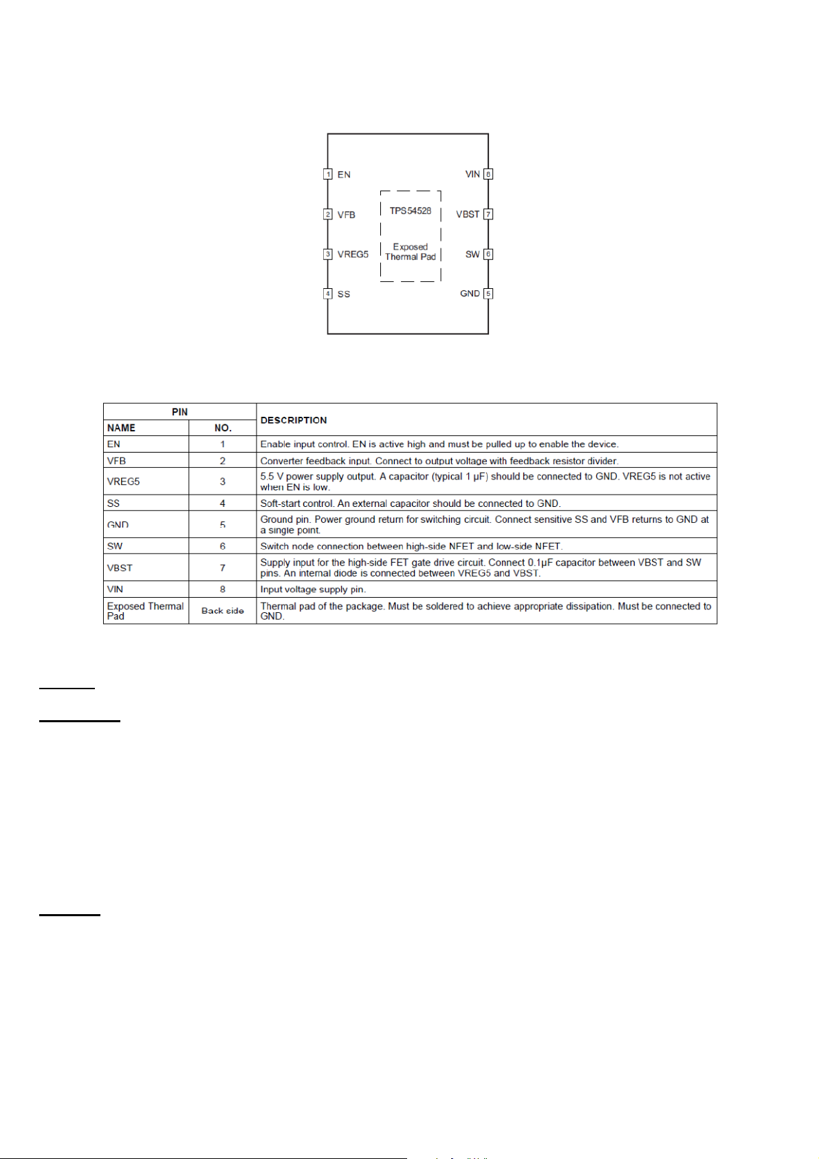
TPS54528
Description
The TPS54528 is an adaptive on-time D-CAP2™ mode synchronous buck converter. The TPS54528 enables
system designers to complete the suite of various end-equipment power bus regulators with a cost effective, low
component count, low standby current solution. The main control loop for the TPS54528 uses the D-CAP2™
mode control that provides a fast transient response with no external compensation components. The adaptive
on-time control supports seamless transition between PWM mode at higher load conditions and Eco-mode™
operation at light loads. Eco-mode™ allows the TPS54528 to maintain high efficiency during lighter load
conditions. The TPS54528 also has a proprietary circuit that enables the device to adopt to both low equivalent
series resistance (ESR) output capacitors, such as POSCAP or SP-CAP, and ultra-low ESR ceramic capacitors.
The device operates from 4.5-V to 18-V VIN input. The output voltage can be programmed between 0.76 V
and 6.0 V. The device also features an adjustable soft start time. The TPS54528 is available in the 8-pin DDA
package, and designed to operate from –40 C to 85 C.
Features
D-CAP2™ Mode Enables Fast Transient Response
Low Output Ripple and Allows Ceramic Output Capacitor
Wide VIN Input Voltage Range: 4.5 V to 18 V
Output Voltage Range: 0.76 V to 6.0 V
Highly Efficient Integrated FETs Optimized for Lower Duty Cycle Applications
o 65 mΩ (High Side) and 36 mΩ (Low Side)
High Efficiency, less than 10 μA at shutdown
High Initial Bandgap Reference Accuracy
Adjustable Soft Start
Pre-Biased Soft Start
17
Page 19
650-kHz Switching Frequency (fSW)
Cycle By Cycle Over Current Limit
Auto-Skip Eco-mode™ for High Efficiency at Light Load
Figure: Pin description
Table: Pin functions
RT7278
Description
The RT7278 is a synchronous step down converter with Advanced Constant On-Time (ACOTTM) mode
control. The ACOTTM provides a very fast transient response with few external components. The low
impedance internal MOSFET supports high efficiency operation with wide input voltage range from 4.5V to
17V. The proprietary circuit of the RT7278 enables to support all ceramic capacitors. The output voltage can be
adjustable between 0.8V and 8V. The soft-start is adjustable by an external capacitor.
Features
ACOT
TM
Mode Enables Fast Transient Response
4.5V to 17V Input Voltage Range
3A Output Current
60mΩ Internal Low Site N-MOSFET
18
Page 20
Advanced Constant On-Time Control
Support All Ceramic Capacitors
Up to 95% Efficiency
700kHz Switching Frequency
Adjustable Output Voltage from 0.8V to 8V
Adjustable Soft-Start
Cycle-by-Cycle Current Limit
Input Under Voltage Lockout
Thermal Shutdown Protection
RoHS Compliant and Halogen Free
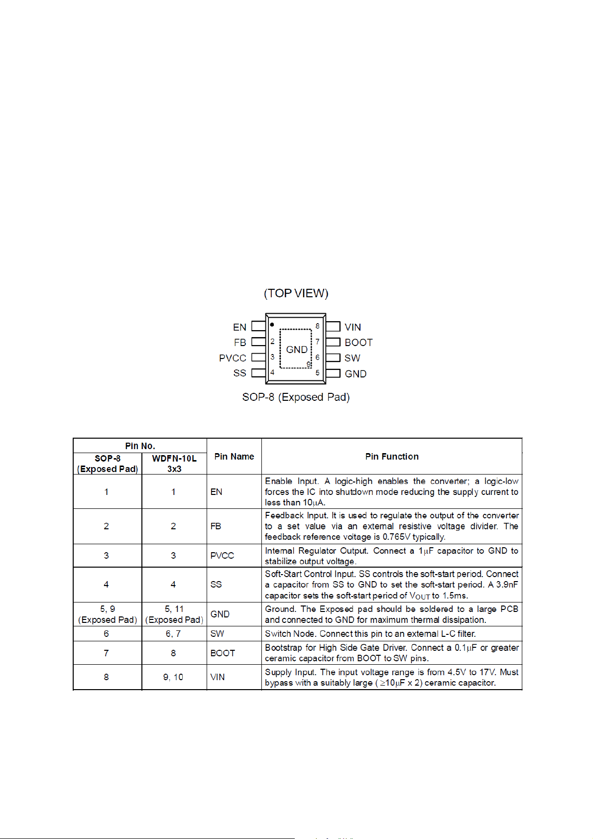
Figure: Pin description
19
Table: Pin functions
Page 21
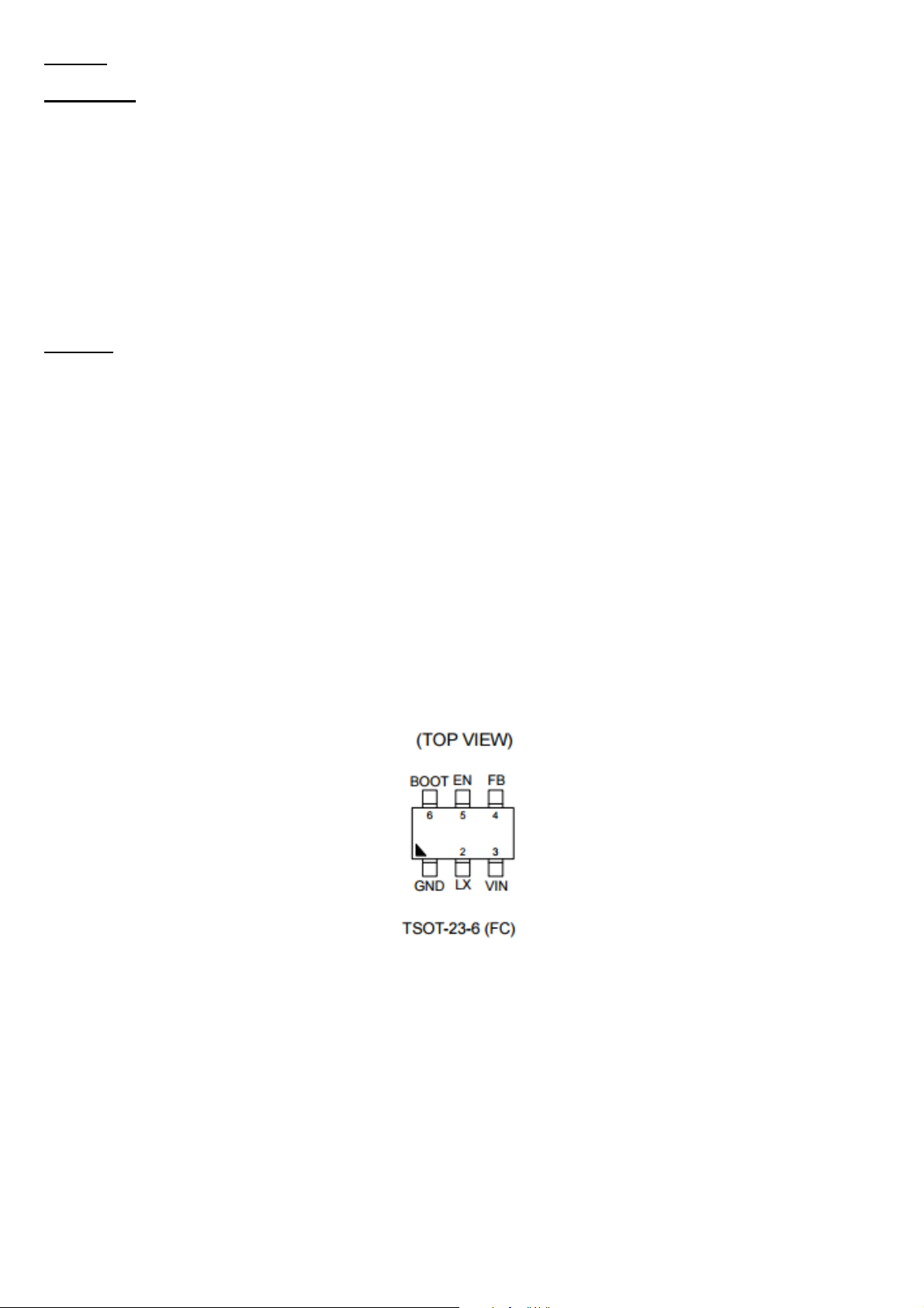
RT6213
Description
The RT6213A/B is a high-efficiency, monolithic synchronous step-down DC/DC converter that can
deliver up to 3A peak output current from a 4.5V to 18V input supply. The RT6213A/B adopts ACOT
architecture to allow the transient response to be improved and keep in constant frequency. Cycle-by-cycle
current limit provides protection against shorted outputs and soft-start eliminates input current surge during
start-up. Fault conditions also include output under voltage protection, output over current protection, and
thermal shutdown.
Features
Integrated 150m/70m MOSFETs
4.5V to 18V Supply Voltage Range
500kHz Switching Frequency
ACOT Control
0.8V 1.5% Voltage Reference
Internal Start-Up into Pre-biased Outputs
Compact Package: TSOT-23-6 pin
Input Under-Voltage Lockout
Over-Current Protection and Hiccup
20
Figure: Pin description
Page 22
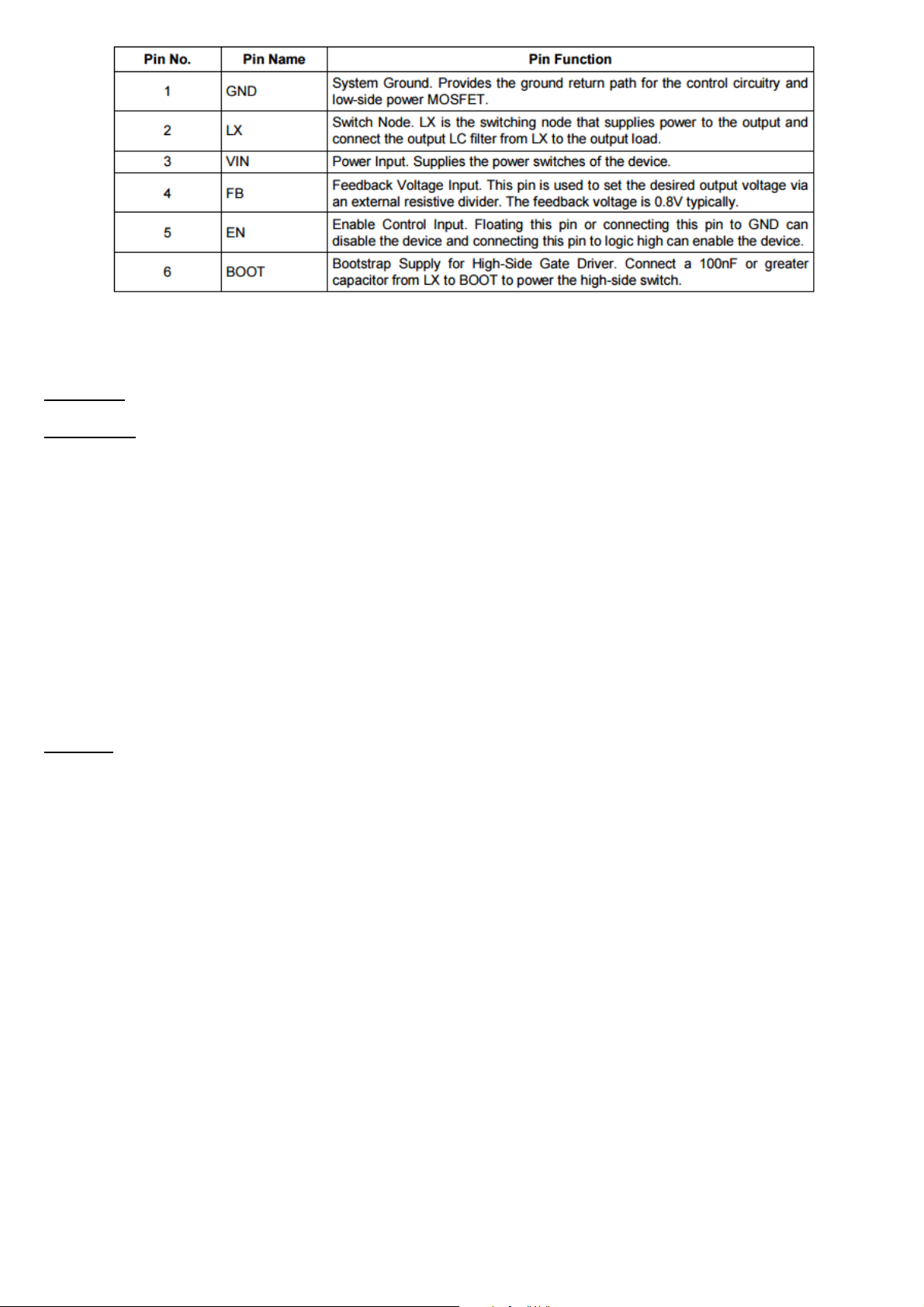
Table: Pin functions
TPS54329
Description
The TPS54329E is an adaptive on-time D-CAP2 mode synchronous buck converter. The TPS54329E
enables system designers to complete the suite of various end-equipment power bus regulators with a cost
effective, low component count, low standby current solution. The main control loop for the TPS54329E uses
the D-CAP2 mode control that provides a fast transient response with no external compensation components.
The adaptive on-time control supports seamless transition between PWM mode at higher load conditions and
Eco-mode™ operation at light loads. Eco-mode™ allows the TPS54329E to maintain high efficiency during
lighter load conditions. The TPS54329E also has a proprietary circuit that enables the device to adopt to both
low equivalent series resistance (ESR) output capacitors, such as POSCAP or SP-CAP, and ultra-low ESR
ceramic capacitors. The device operates from 4.5-V to 18-V VIN input. The output voltage can be programmed
between 0.76 V and 7 V. The device also features an adjustable soft start time. The TPS54329E is available in
the 8-pin DDA package, and designed to operate from –40°C to 85°C.
Features
D-CAP2™ Mode Enables Fast Transient Response
Low Output Ripple and Allows Ceramic Output Capacitor
Wide V
Input Voltage Range: 4.5 V to 18 V
IN
Output Voltage Range: 0.76 V to 7.0 V
Highly Efficient Integrated FETs Optimized for Lower Duty Cycle Applications
– 100 mΩ (High Side) and 74 mΩ (Low Side)
High Efficiency, less than 10 µA at shutdown
High Initial Bandgap Reference Accuracy
Adjustable Soft Start
Pre-Biased Soft Start
650-kHz Switching Frequency (f
SW
)
Cycle By Cycle Over Current Limit
Auto-Skip Eco-mode™ for High Efficiency at Light Load
21
Page 23
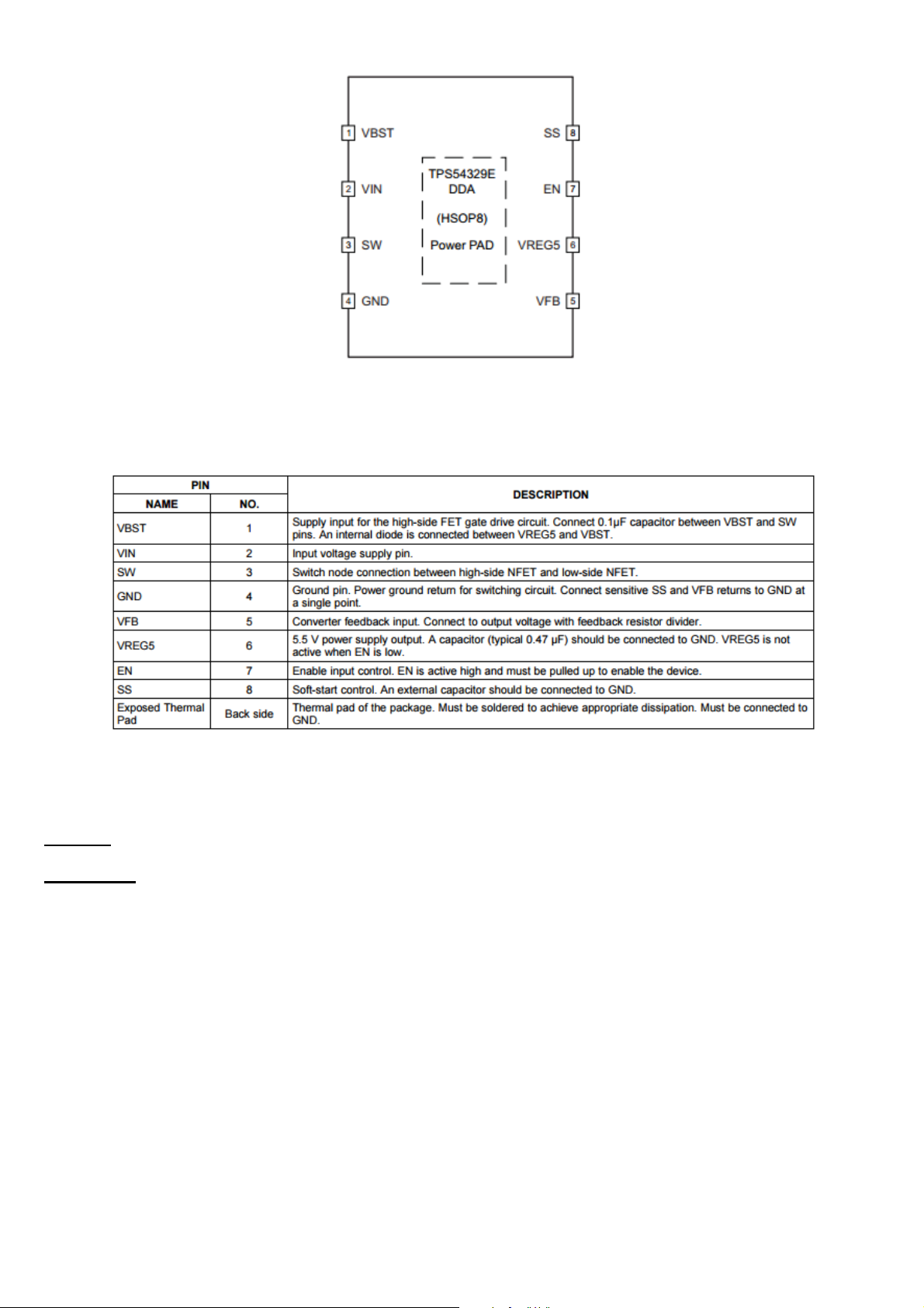
Figure: Pin description
Table: Pin functions
LM1117
Description
The LM1117 is a series of low dropout voltage regulators with a dropout of 1.2V at 800mA of load current.
It has the same pin-out as National Semiconductor’s industry Standard LM317.
The LM1117 is available in an adjustable version, which can set the output voltage from 1.25V to 13.8V
with only two external resistors. In addition, it is also available in five fixed voltages, 1.8V, 2.5V, 2.85V, 3.3V,
and 5V.
The LM1117 offers current limiting and thermal shutdown. Its circuit includes a zener trimmed bandgap
reference to assure output voltage accuracy to within ±1%.
The LM1117 series is available in SOT-223, TO-220, and TO-252 D-PAK packages. A minimum of 10μF
tantalum capacitor is required at the output to improve the transient response and stability.
22
Page 24
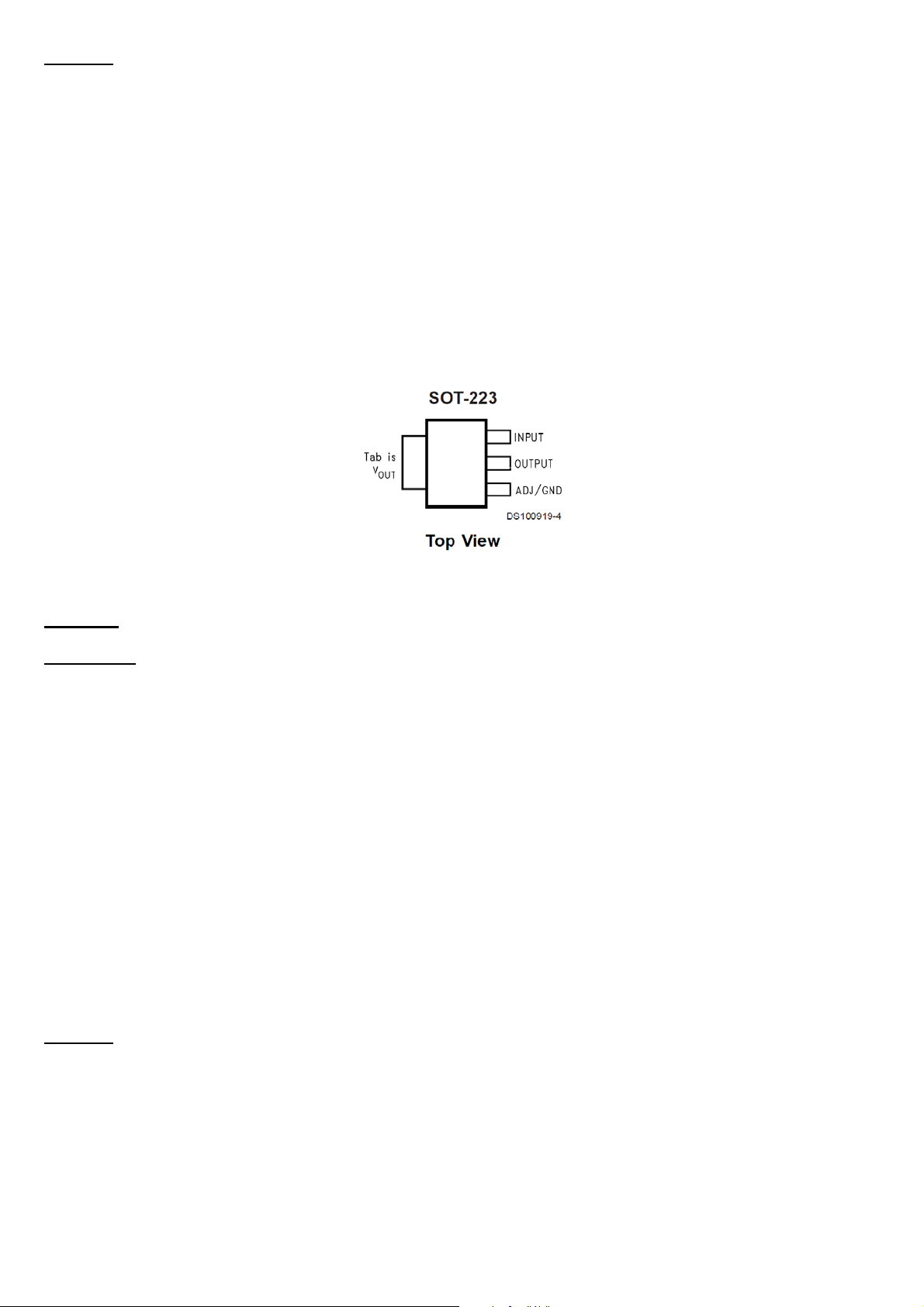
Features
Available in 1.8V, 2.5V, 2.85V, 3.3V, 5V, and Adjustable Versions
Space Saving SOT-223 Package
Current Limiting and Thermal Protection
Output Current 800mA
Line Regulation 0.2% (Max)
Load Regulation 0.4% (Max)
Temperature Range
— LM1117 0°C to 125°C
— LM1117I −40°C to 125°C
Figure: Pin description
APL5910
Description
The APL5910 is a 1A ultra low dropout linear regulator. The IC needs two supply voltages, one is a control
voltage (VCNTL) for the control circuitry, the other is a main supply voltage (VIN) for power conversion, to
reduce power dissipation and provide extremely low dropout voltage. The APL5910 integrates many functions.
A Power-On- Reset (POR) circuit monitors both supply voltages on VCNTL and VIN pins to prevent erroneous
operations. The functions of thermal shutdown and current-limit protect the device against thermal and current
over-loads. A POK indicates that the output voltage status with a delay time set internally. It can control other
converter for power sequence. The APL5910 can be enabled by other power systems. Pulling and holding the
EN voltage below 0.4V shuts off the output.
The APL5910 is available in a SOP-8P package which features small size as SOP-8 and an Exposed Pad to
reduce the junction-to-case resistance to extend power range of applications.
Features
Ultra Low Dropout
o 0.12V (Typical) at 1AOutput Current
0.8V Reference Voltage
High Output Accuracy
23
Page 25
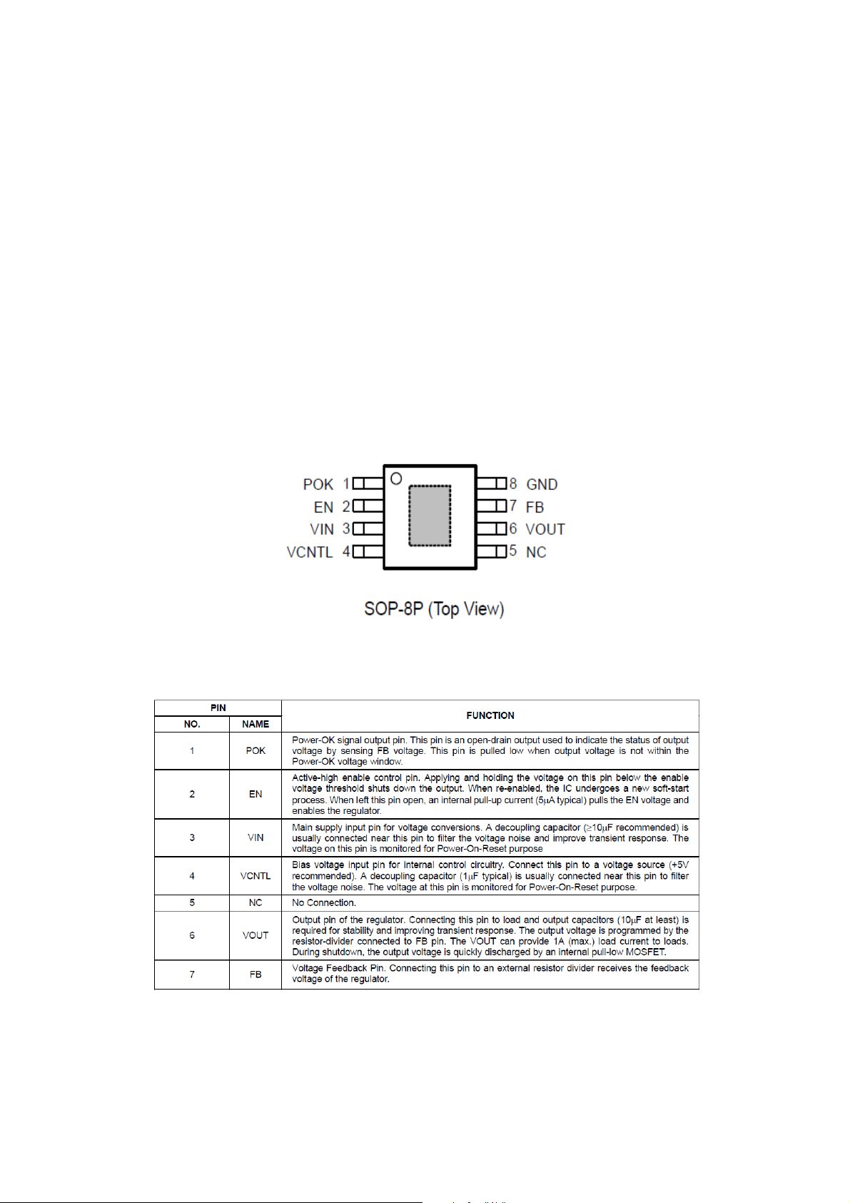
o ±1.5%over Line, Load, and Temperature Range
Fast Transient Response
Adjustable Output Voltage
Power-On-Reset Monitoring on Both VCNTL and VIN Pins
Internal Soft-Start
Current-Limit and ShortCurrent-Limit Protections
Thermal Shutdown with Hysteresis
Open-Drain VOUT Voltage Indicator (POK)
Low Shutdown Quiescent Current (< 30mA )
Shutdown/Enable Control Function
Simple SOP-8P Package with Exposed Pad
Lead Free and Green Devices Available (RoHS Compliant)
Figure: Pin description
Table: Pin functions
24
Page 26
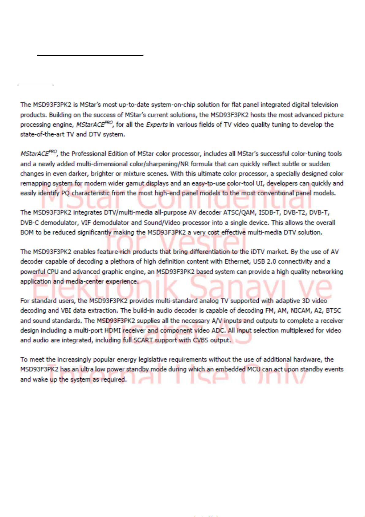
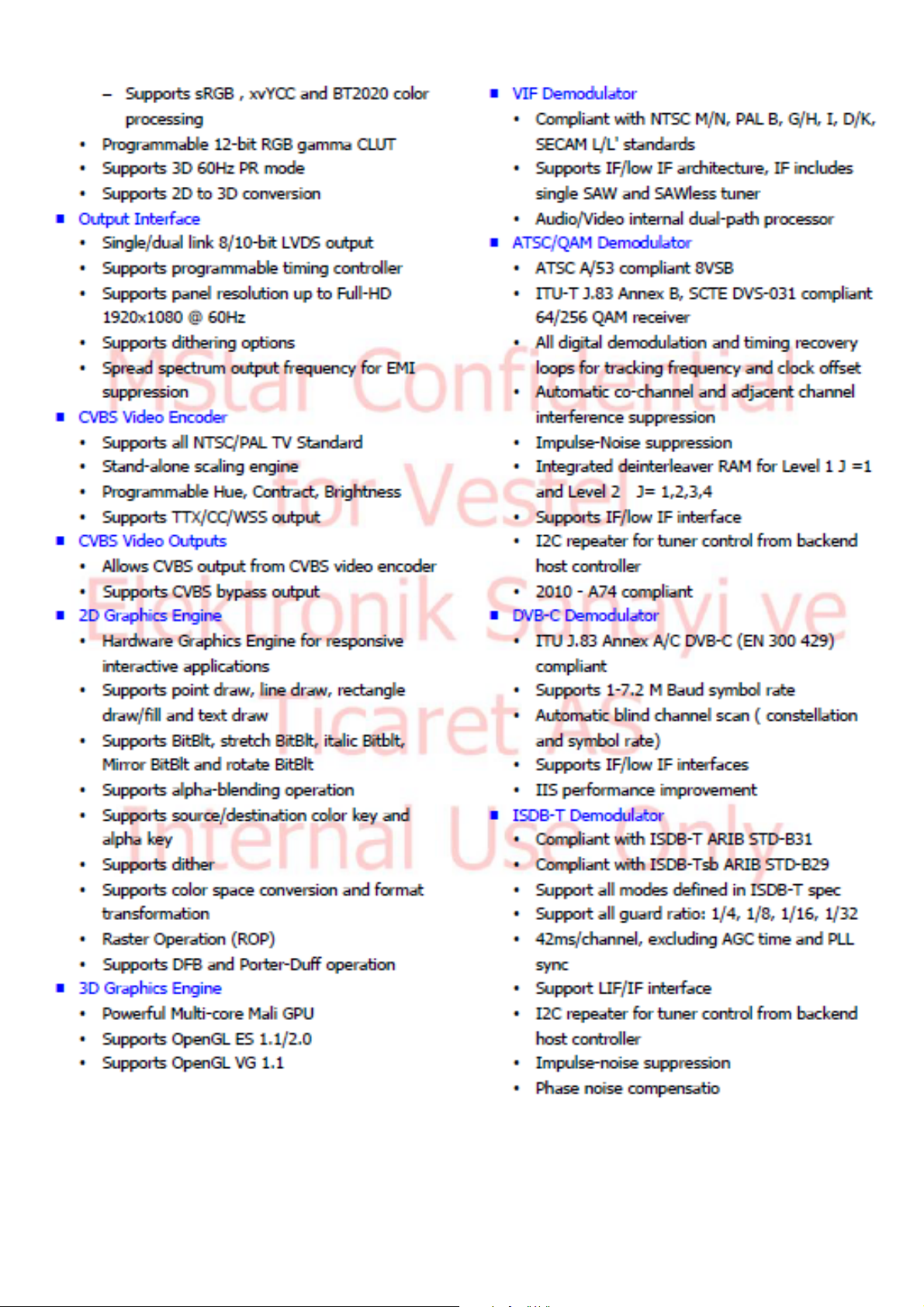
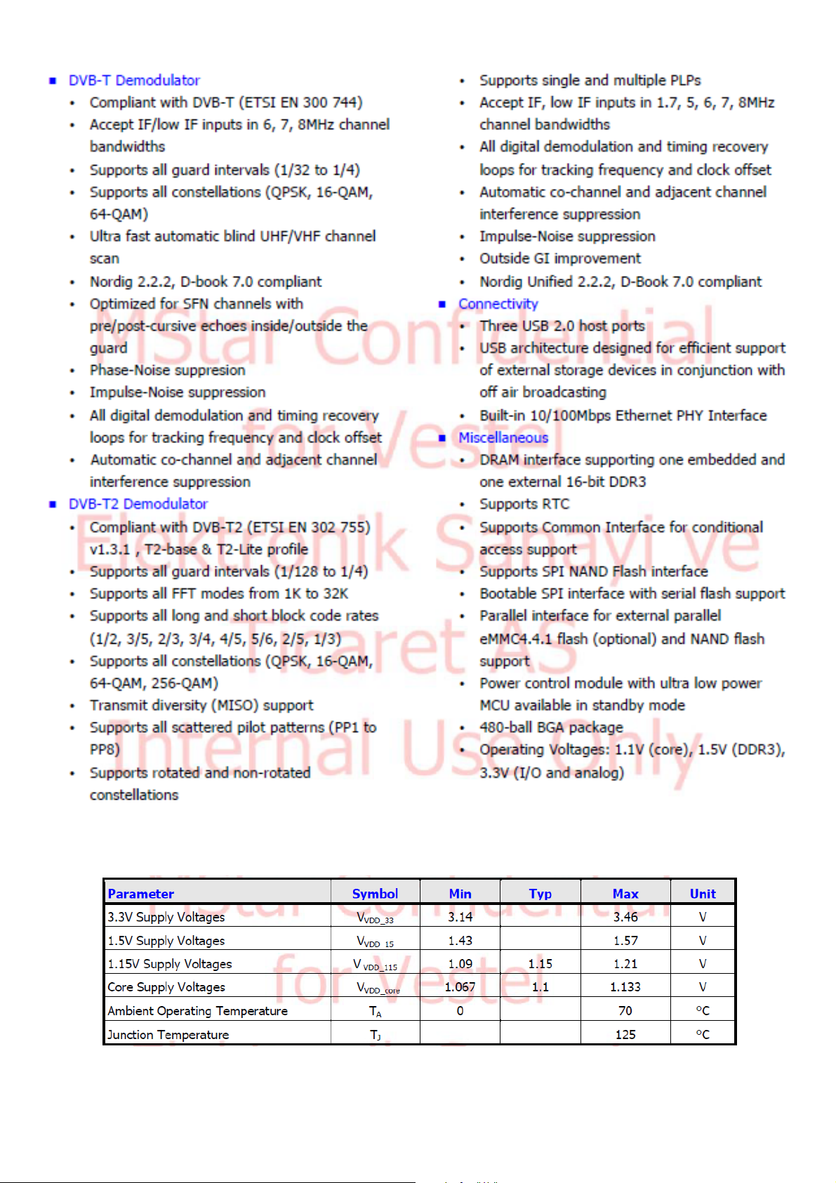
6. MICROCONTROLLER
A. MSTAR MSD93F3PK2 (U95)
Description
25
Page 27
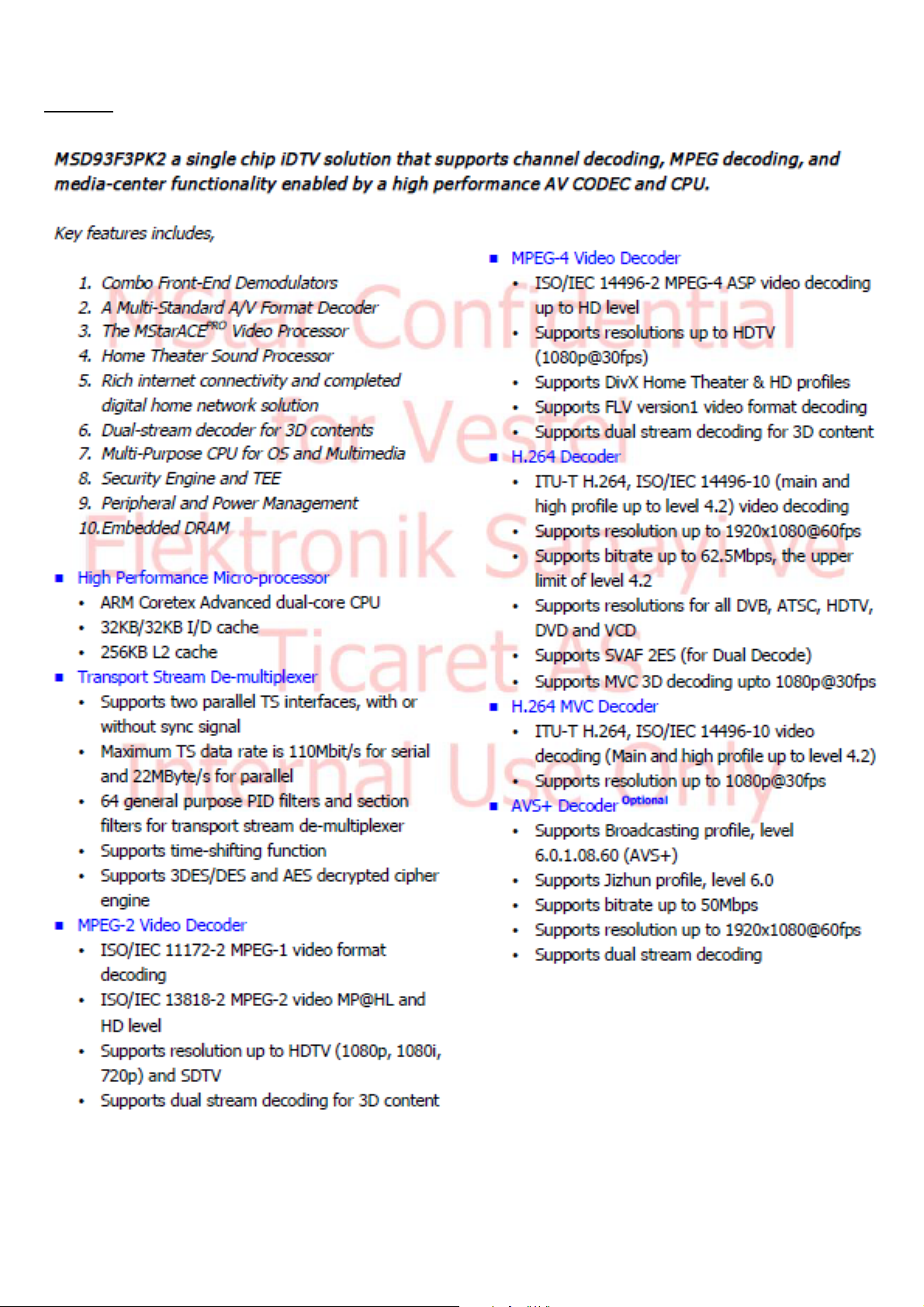
Features
26
Page 28
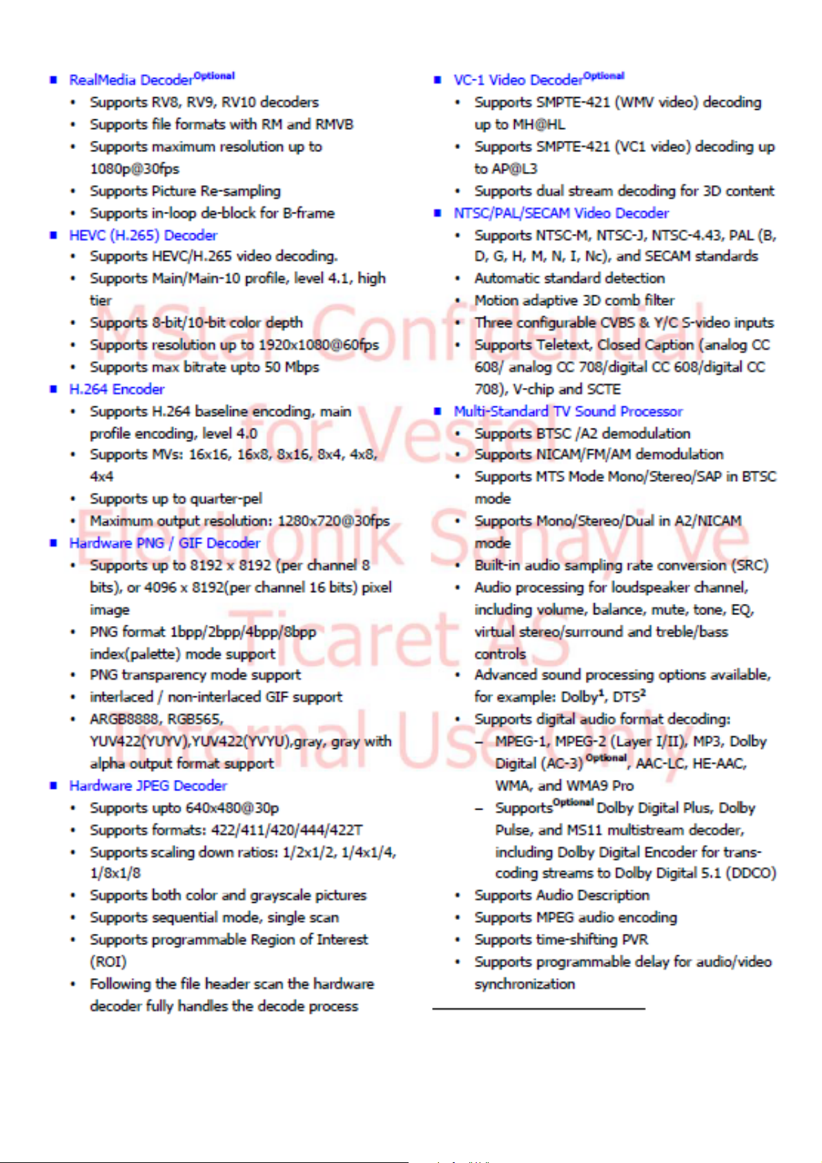
27
Page 29
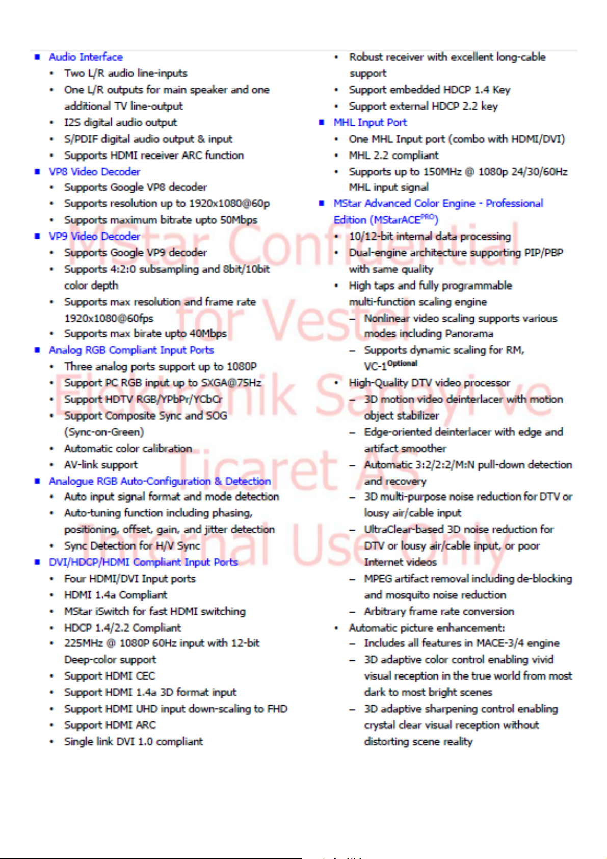
28
Page 30
29
Page 31
30
Table: Recommended operating conditions
Page 32

7. 4GB DDR3 SDRAM
A. SAMSUNG K4B4G1646D (U72)
Description
The 4Gb DDR3 SDRAM D-die is organized as a 32Mbit x 16 I/Os x 8banks, device. This synchronous
device achieves high speed double-data-rate transfer rates of up to 2133Mb/sec/pin (DDR3-2133) for general
applications. The chip is designed to comply with the following key DDR3 SDRAM features such as posted
CAS, Programmable CWL, Internal (Self) Calibration, On Die Termination using ODT pin and Asynchronous
Reset . All of the control and address inputs are synchronized with a pair of externally supplied differential
clocks. Inputs are latched at the crosspoint of differential clocks (CK rising and CK falling). All I/Os are
synchronized with a pair of bidirectional strobes (DQS and DQS) in a source synchronous fashion. The address
bus is used to convey row, column and bank address information in a RAS/CAS multiplexing style. The DDR3
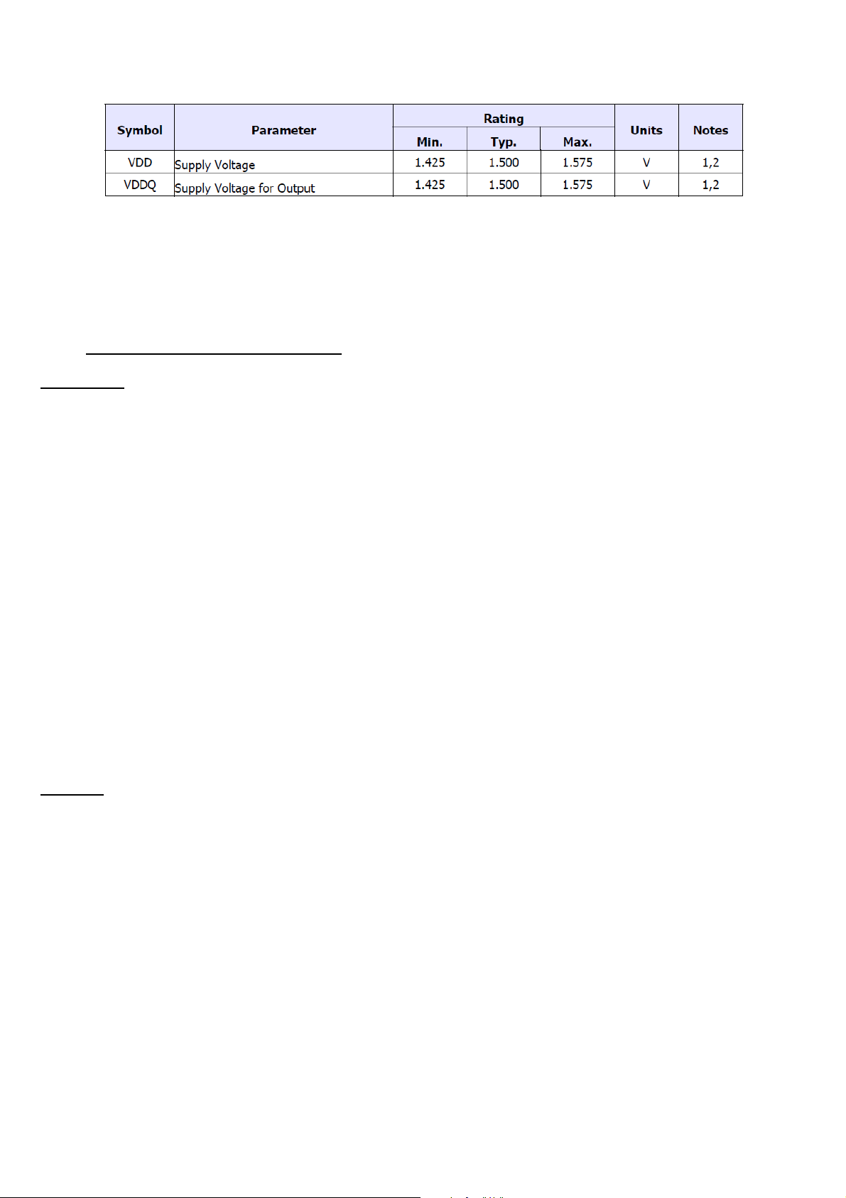
device operates with a single 1.5V(1.425V~1.575V)power supply and 1.5V(1.425V~1.575V) VDDQ. The 4Gb
DDR3 D-die device is available in 96ball FBGAs(x16)..
Features
JEDEC standard 1.5V(1.425V~1.575V)
VDDQ = 1.5V(1.425V~1.575V)
400 MHz fCK for 800Mb/sec/pin, 533MHz fCK for 1066Mb/sec/pin, 667MHz fCK for
1333Mb/sec/pin, 800MHz fCK for 1600Mb/sec/pin, 933MHz fCK for 1866Mb/sec/pin, 1066 MHz fCK
for 2133Mb/sec/pin
8 Banks
Programmable CAS Write Latency (CWL) = 5 (DDR3-800), 6 (DDR3-1066), 7 (DDR3-1333) , 8
(DDR3-1600), 9 (DDR3-1866) and 10 (DDR3-2133)
8-bit pre-fetch
Burst Length: 8 (Interleave without any limit, sequential with starting address “000” only), 4 with tCCD
= 4 which does not allow seamless read or write [either On the fly using A12 or MRS]
Bi-directional Differential Data-Strobe
Internal(self) calibration : Internal self calibration through ZQ pin (RZQ : 240 ohm ± 1%)
On Die Termination using ODT pin
Average Refresh Period 7.8us at lower than TCASE 85C, 3.9us at 85C < TCASE < 95 C
Support Industrial Temp ( -4095C ) - tREFI 7.8us at -40 °C ≤ TCASE ≤ 85°C - tREFI 3.9us at 85 °C
< TCASE ≤ 95°C
Asynchronous Reset
Package : 96 balls FBGA - x16
All of Lead-Free products are compliant for RoHS
31
Page 33
All of products are Halogen-free
Table: Recommended operating conditions
8. 4GBİT (256M X 8 BİT) NAND FLASH MEMORY
A. MT29F4G08ABAEAWP (U80)
Description
Micron NAND Flash devices include an asynchronous data interface for high-performance I/O operations.
These devices use a highly multiplexed 8-bit bus (I/Ox) to transfer commands, address, and data. There are five
control signals used to implement the asynchronous data interface: CE#, CLE, ALE, WE#, and RE#. Additional
signals control hardware write protection and monitor device status (R/B#). This hardware interface creates a
low pin-count device with a standard pinout that remains the same from one density to another, enabling future
upgrades to higher densities with no board redesign. A target is the unit of memory accessed by a chip enable
signal. A target contains one or more NAND Flash die. A NAND Flash die is the minimum unit that can
independently execute commands and report status. A NAND Flash die, in the ONFI specification, is referred
to as a logical unit (LUN). There is at least one NAND Flash die per chip enable signal. For further details, see
Device and Array Organization. This device has an internal 4-bit ECC that can be enabled using the GET/SET
features or by factory (always enabled). See Internal ECC and Spare Area Mapping for ECC for more
information.
Features
Open NAND Flash Interface (ONFI) 1.0-compliant
Single-level cell (SLC) technology
Organization
o Page size x8: 4320 bytes (4096 + 224 bytes)
o Page size x16: 2160 words (2048 + 112 words)
o Block size: 64 pages (256K + 14K bytes)
o Plane size: 2 planes x 1024 blocks per plane
o Device size: 4Gb: 2048 blocks
Asynchronous I/O performance
t
o
RC/tWC: 20ns (3.3V), 30ns (1.8V)
32
Page 34

Array performance
o Read page: 25μs
o Program page: 200μs (TYP)
o Erase block: 2ms (TYP)
Command set: ONFI NAND Flash Protocol
Advanced command set
o Program page cache mode
o Read page cache mode
o One-time programmable (OTP) mode
o Programmable drive strength
o Two-plane commands
o Multi-die (LUN) operations
o Read unique ID
o Block lock (1.8V only)
o Internal data move
Operation status byte provides software method for detecting
o Operation completion
o Pass/fail condition
o Write-protect status
Ready/Busy# (R/B#) signal provides a hardware method of detecting operation completion
WP# signal: Write protect entire device
First block (block address 00h) is valid when shipped from factory with ECC. For minimum required
ECC, see Error Management.
RESET (FFh) required as first command after power-on
Alternate method of device initialization after power up (contact factory)
Internal data move operations supported within the plane from which data is read
Quality and reliability
o Data retention: JESD47G-compliant; see qualification report
o Endurance: See Qualification Report
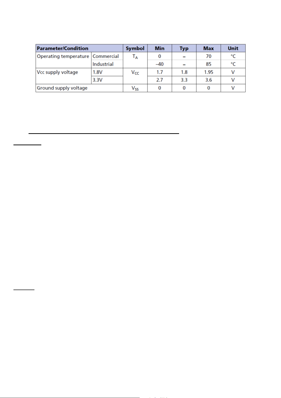
Operating voltage range
o VCC: 2.7–3.6V
o VCC: 1.7–1.95V
Operating temperature:
o Commercial: 0°C to +70°C
o Industrial (IT): –40ºC to +85ºC
Package
33
Page 35
o 48-pin TSOP type 1, CPL2
o 63-ball VFBGA
Table: Recommended operating conditions
9. 16M-BIT [16M X 1] CMOS SERIAL FLASH EEPROM
A. KH25L1606EM2-12G MACRONİX SPI FLASH (U81)
Description
The device features a serial peripheral interface and software protocol allowing operation on a simple 3-wire
bus. The three bus signals are a clock input (SCLK), a serial data input (SI), and a serial data output (SO).
Serial access to the device is enabled by CS# input. When it is in Dual Output read mode, the SI and SO pins
become SIO0 and SIO1 pins for data output. The device provides sequential read operation on whole chip.
After program/erase command is issued, auto program/erase algorithms which program/erase and verify the
specified page or sector/block locations will be executed. Program command is executed on byte basis, or page
basis, or word basis for erase command is executes on sector, or block, or whole chip basis. To provide user
with ease of interface, a status register is included to indicate the status of the chip. The status read command
can be issued to detect completion status of a program or erase operation via WIP bit. Advanced security
features enhance the protection and security functions; please see security features section for more details.
When the device is not in operation and CS# is high, it is put in standby mode. The device utilizes
Macronix's proprietary memory cell, which reliably stores memory contents even after typical 100,000
programs and erase cycles.
Features
Single Power Supply Operation
o 2.7 to 3.6 volt for read, erase, and program operations
Serial Peripheral Interface compatible -- Mode 0 and Mode 3
16,777,216 x 1 bit structure or 8,388,608 x 2 bits (Dual Output mode) structure
512 Equal Sectors with 4K byte each
o
Any Sector can be erased individually
32 Equal Blocks with 64K byte each
o
Any Block can be erased individually
34
Page 36
Program Capability
Byte base
o
o
Page base (256 bytes)
Latch-up protected to 100mA from -1V to Vcc +1V
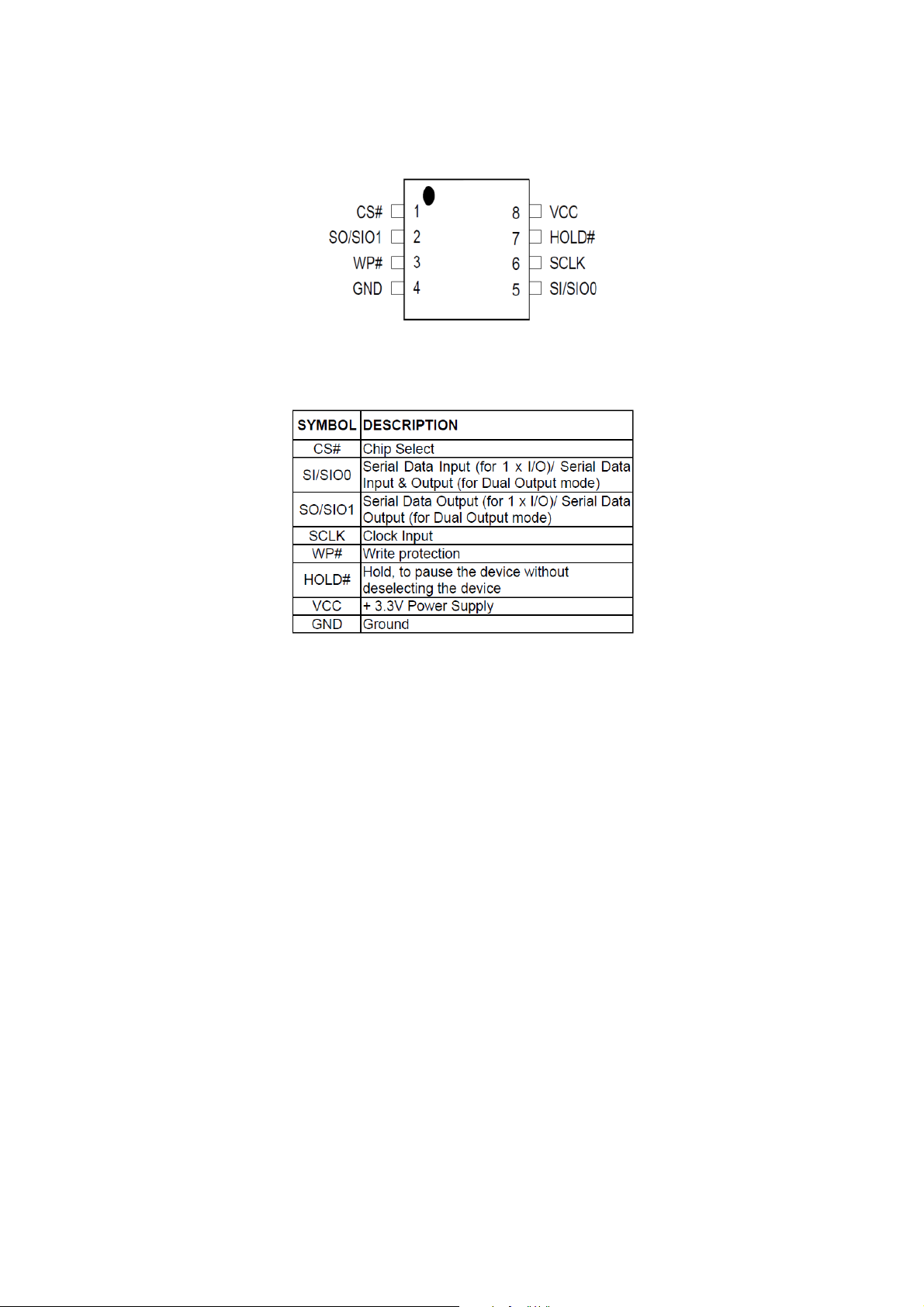
Figure: Pin configuration
Table: Pin description
35
Page 37
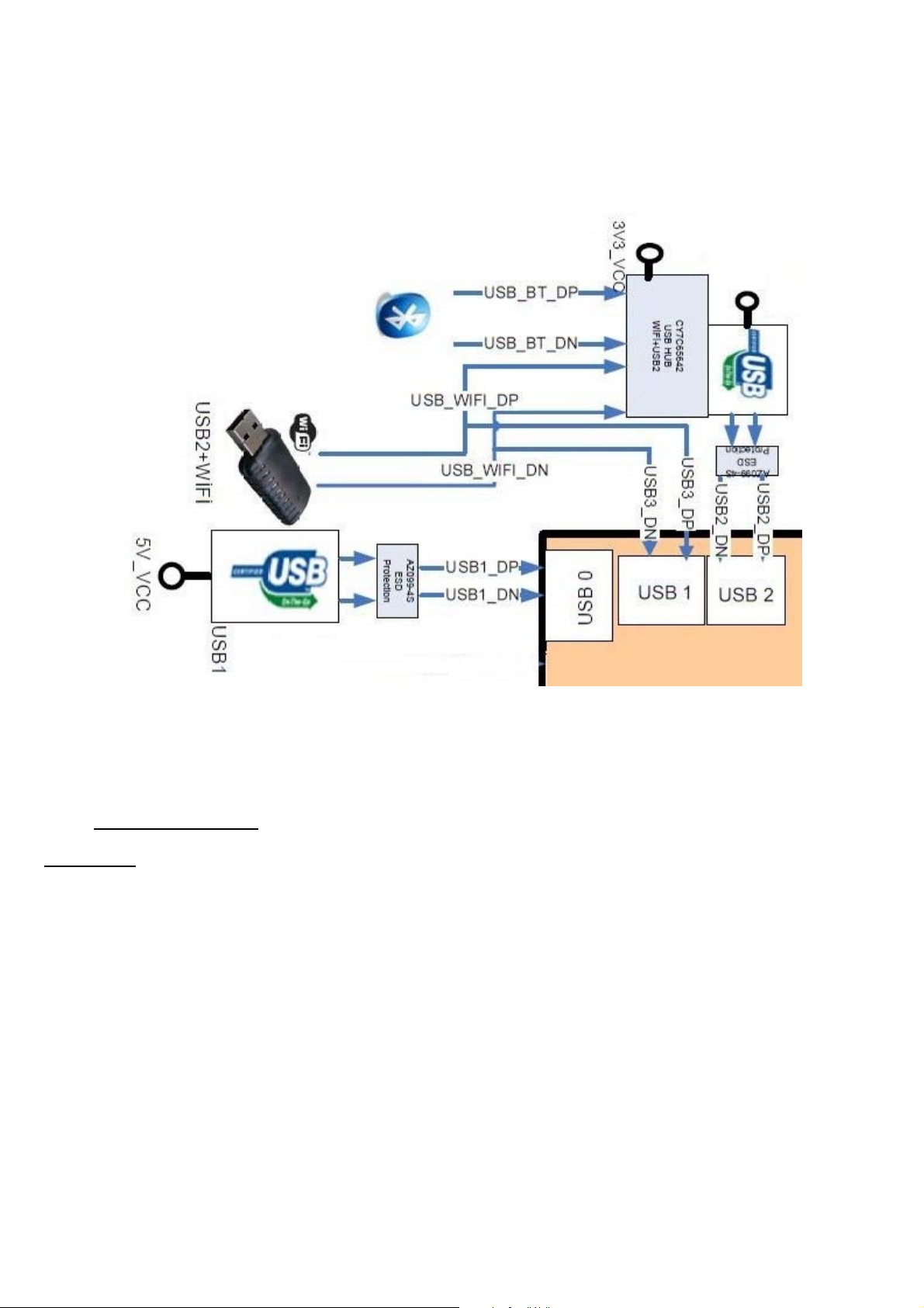
10. USB INTERFACE
Mstar IC has three input port for USB, therefore internal Bluetooth, internal Wi-Fi interface are combined
with HUB. This property is optional. If Bluetooth and Wi-Fi interfaces are not alined, three USB are connected
directly to main IC.
Figure: USB Block Diagram
A. CY7C65642 (U73)
Description
HX2VL is Cypress’s next generation family of high- performance, very low-power USB 2.0 hub controllers.
HX2VL has integrated upstream and downstream transceivers; a USB serial interface engine (SIE); USB hub
control and repeater logic; and transaction translator (TT) logic. Cypress has also integrated external
components such as voltage regulator and pull-up/pull-down resistors, reducing the overall BOM required to
implement a USB hub system. The CY7C65642 is a part of the HX2VL portfolio with four downstream ports
and an independent TT dedicated for each downstream port. This device option is for low-power but high-
performance applications that require up to four downstream ports. The CY7C65642 is available in 48-pin
TQFP and 28-pin QFN package options.
36
Page 38

Features
High-performance, low-power USB 2.0 hub, optimized for low-cost designs with minimum bill-of-material (BOM).
USB 2.0 hub controller
o Compliant with USB2.0 specification
o Up to four downstream ports support
o Downstream ports are backward compatible with FS, LS
o Multiple translators (TT), one per downstream port for maximum performance.
Very low-power consumption
o Supports bus-powered and self-powered modes
o Auto switching between bus-powered and self-powered
o Single MCU with 2K ROM and 64 byte RAM
o Lowest power consumption.
Highly integrated solution for reduced BOM cost
o Internal regulator – single power supply 5 V required.
o Provision of connecting 3.3 V with external regulator.
o Integrated upstream pull-up resistor
o Integrated pull-down resistors for all downstream ports
o Integrated upstream/downstream termination resistors
o Integrated port status indicator control
o 12-MHz +/-500 ppm external crystal with drive level 600uW (integrated PLL) clock input with optional 27/48-MHz
oscillator clock input.
o Internal power failure detection for ESD recovery
Downstream port management
o Support individual and ganged mode power management
o Overcurrent detection
o Two status indicators per downstream port
o Slew rate control for EMI management
Maximum configurability
o VID and PID are configurable through external EEPROM
o Number of ports, removable/non-removable ports are configurable through EEPROM and I/O pin configuration
o I/O pins can configure gang/individual mode power switching, reference clock source and polarity of power switch
enable pin
o Configuration options also available through mask ROM
o Available in space saving 48-pin TQFP (7 × 7 mm) and 28-pin QFN (5 × 5 mm) packages
o
o Supports 0
C to +70oC temperature range
37
Page 39
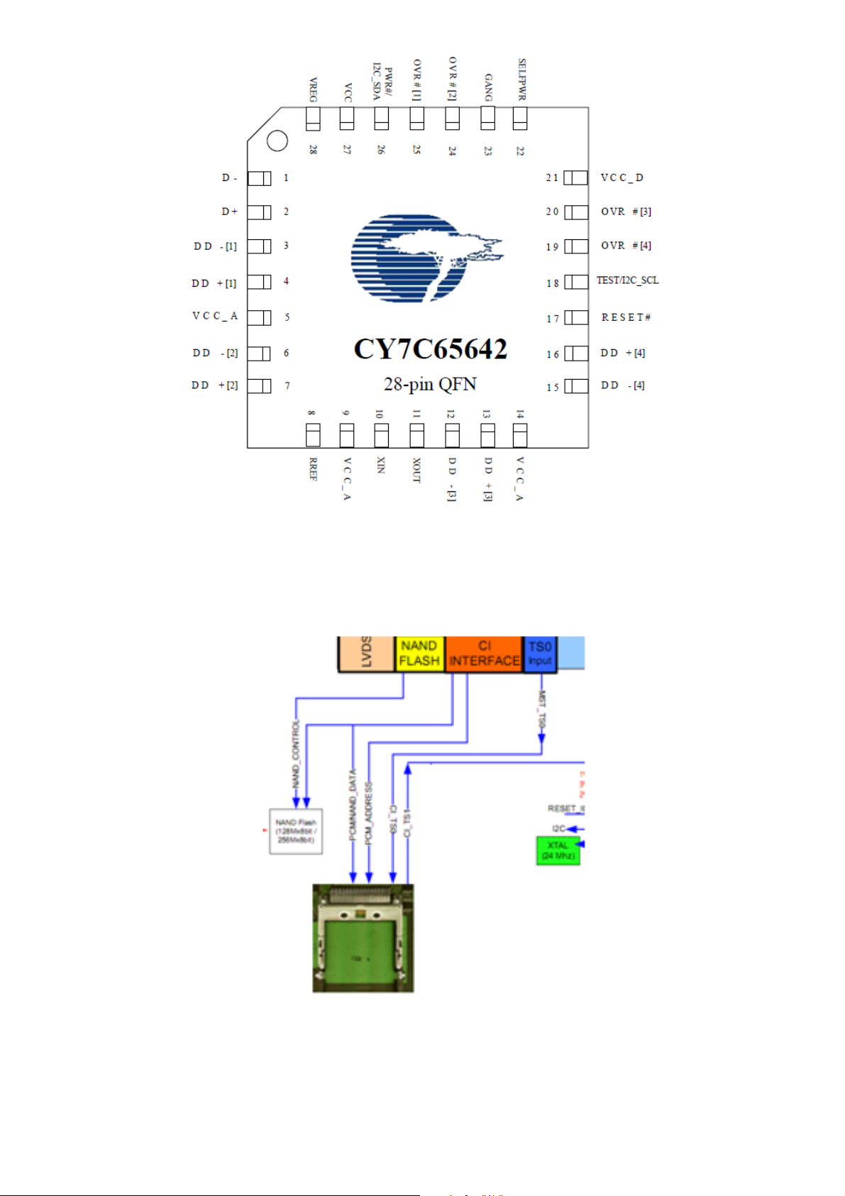
Figure: Pin configuration
11. CI INTERFACE
17MB110 Digital CI ve Smart Card Interface Block diagram:
38
Figure: CI interface
Page 40
12. SOFTWARE UPDATE
A. MAIN SW UPDATE
In MB110 project, please follow software update procedure:
1. mb110_en.bin, mb110_RomBoot.bin, mb110_PM51.bin and usb_auto_update_G7.txt files should be
copied directly inside of a flash memory (not in a folder).
2. Insert flash memory to the TV when TV is powered off.
3. While pushing the OK button in remote control, power on and wait. TV will power-up itself.
4. If First Time Installation screen comes, it means software update procedure is successful.
13. TROUBLESHOOTING
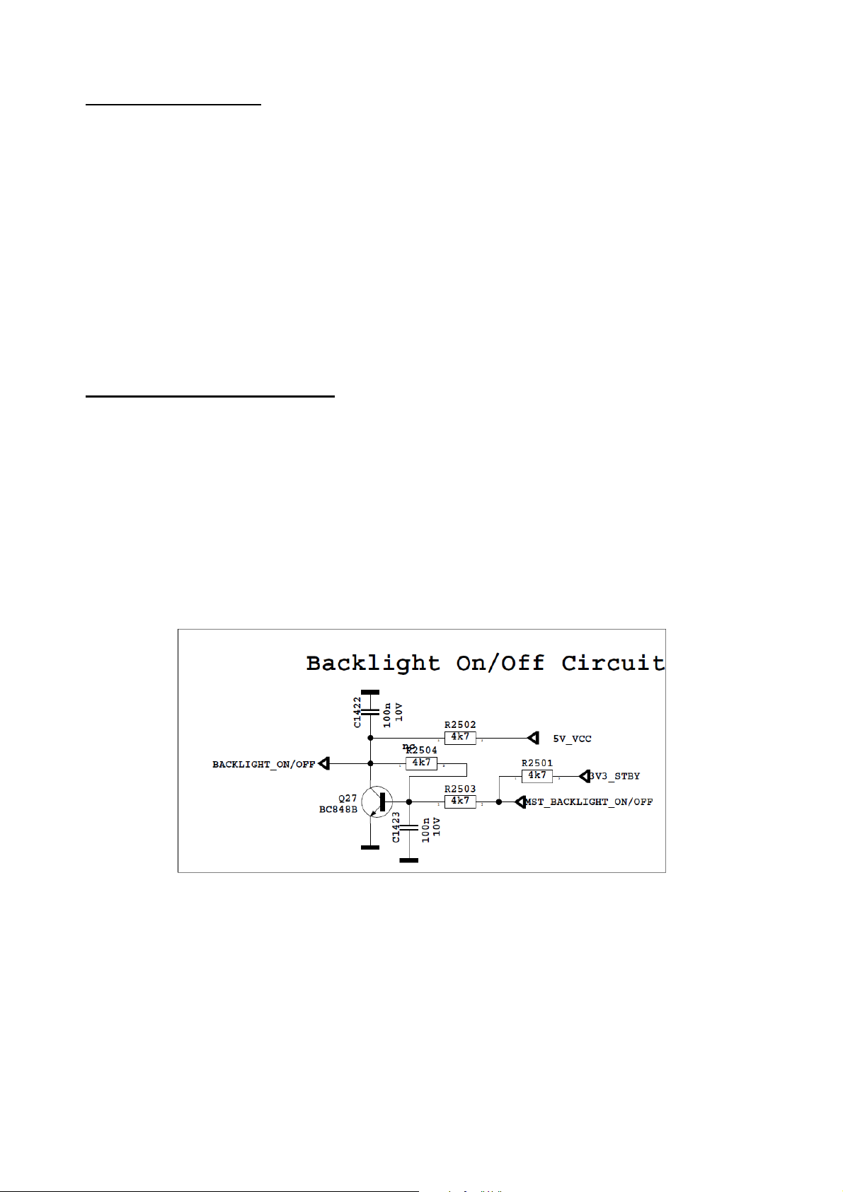
A. NO BACKLIGHT PROBLEM
Problem: If TV is working, led is normal and there is no picture and backlight on the panel.
Possible causes: Backlight pin, dimming pin, backlight supply, stby on/off pin
BACKLIGHT_ON/OFF pin should be high when the backlight is ON. Collector pin of Q27 must be low when
the backlight is OFF. If it is a problem, please check Q27 and the panel cables. Also it can be tested in TP87 in
main board.
Dimming pin should be high or square wave in open position. If it is low, please check S248 for Mstar
side and panel or power cables, connectors.
39
Page 41
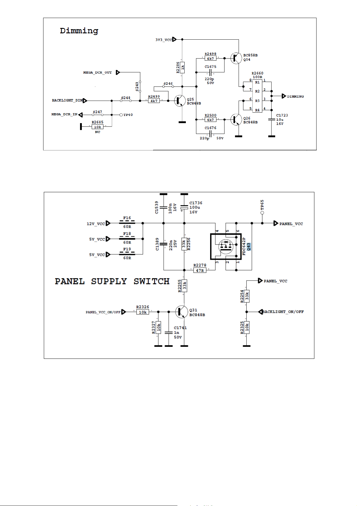
Backlight power supply should be in panel specs. Please check Q43, shown below; also it can be checked
TP65.
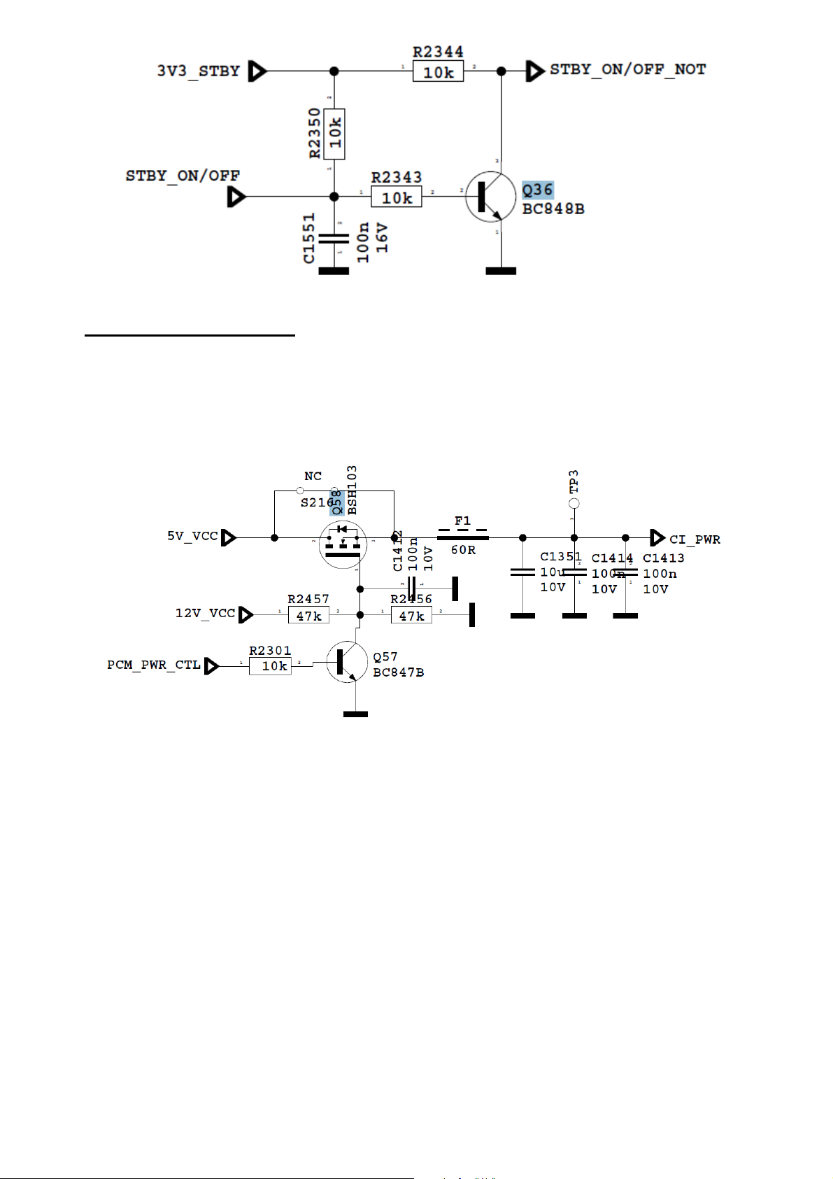
STBY_ON/OFF should be low for TV on condition, please check Q36’s collector.
40
Page 42
B. CI MODULE PROBLEM
Problem: CI is not working when CI module inserted.
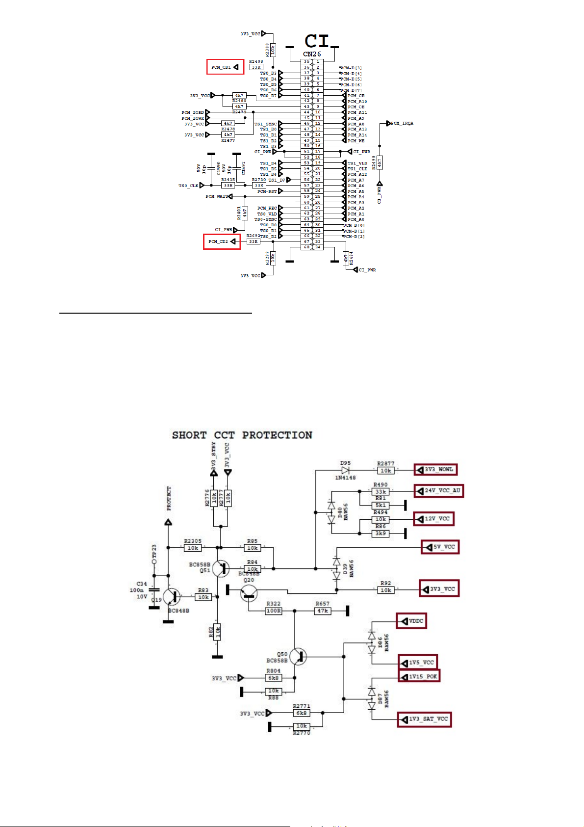
Possible causes: Supply, suply control pin, detects pins, mechanical positions of pins.
CI supply should be 5V when CI module inserted. If it is not 5V please check CI_PWR_CTRL, this pin
should be low.
Please check mechanical position of CI module. Is it inserted properly or not?
Detect ports should be low. If it is not low please check CI connector pins, CI module pins.
41
Page 43
C. STAYING IN STAND-BY MODE
Problem: Staying in stand-by mode, no other operation.
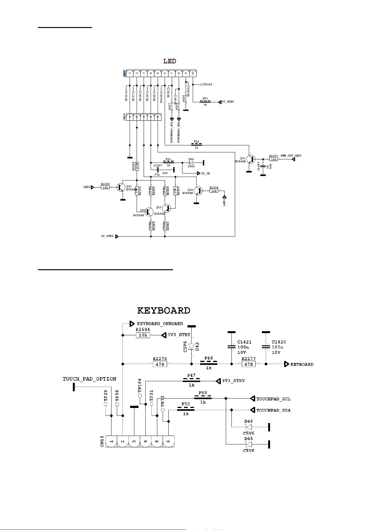
This problem indicates a short on Vcc voltages. Protect pin should be logic high while normal operation. When
there is a short circuit protect pin will be logic low. If you detect logic low on protect pin, unplug the TV set
and control voltage points with a multimeter to find the shorted voltage to ground.
42
Page 44
D. IR PROBLEM
Problem: LED or IR not working
Check LED card supply on MB110 chasis.
E. KEYPAD TOUCHPAD PROBLEMS
Problem: Keypad or Touchpad is not working
Check keypad supply on MB110.
43
Page 45
F. USB PROBLEMS
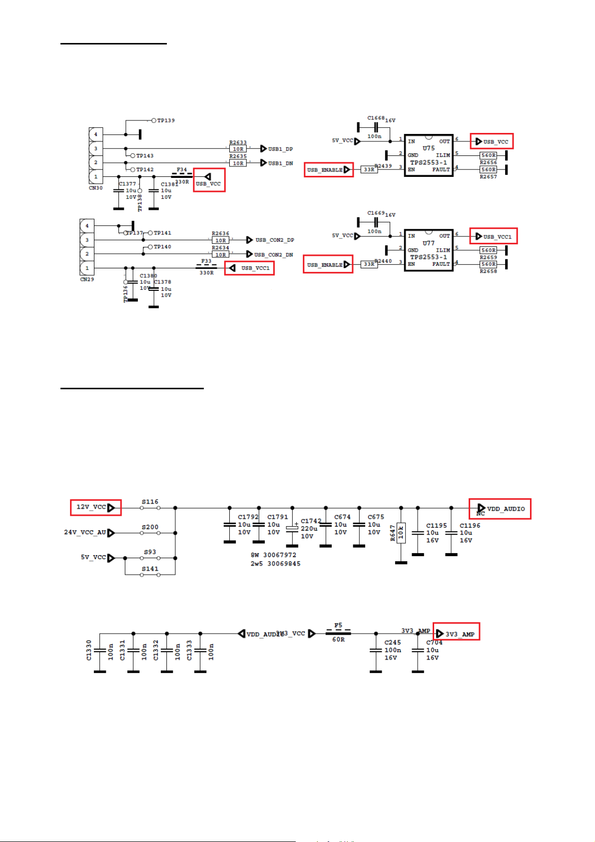
Problem: USB is not working or no USB Detection.
Check USB Supply, It should be nearly 5V. Also USB Enable should be logic high.
G. NO SOUND PROBLEM
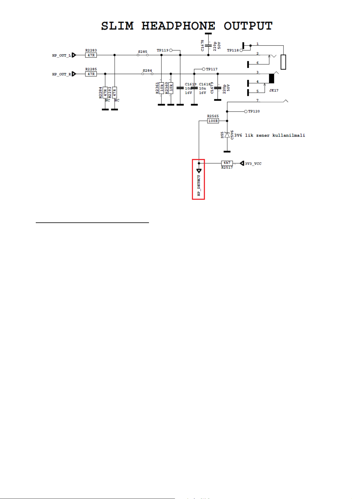
Problem: No audio at main TV speaker outputs.
Check supply voltages of 12V_VCC, VDD_AUDIO and 3V3_AMP with a voltage-meter. There may be a
problem in headphone connector or headphone detect circuit (when headphone is connected, speakers are
automatically muted). Measure voltage at HP_DETECT pin, it should be 3.3v.
44
Page 46
H. STANDBY ON/OFF PROBLEM
Problem: Device can not boot, TV hangs in standby mode.
There may be a problem about power supply. Check main supplies with a voltage-meter. Also there may be a
problem about SW. Try to update TV with latest SW. Additionally it is good to check SW printouts via
Teraterm. These printouts may give a clue about the problem. You can use Scart-1 for terraterm connection.
45
Page 47
I. NO SIGNAL PROBLEM
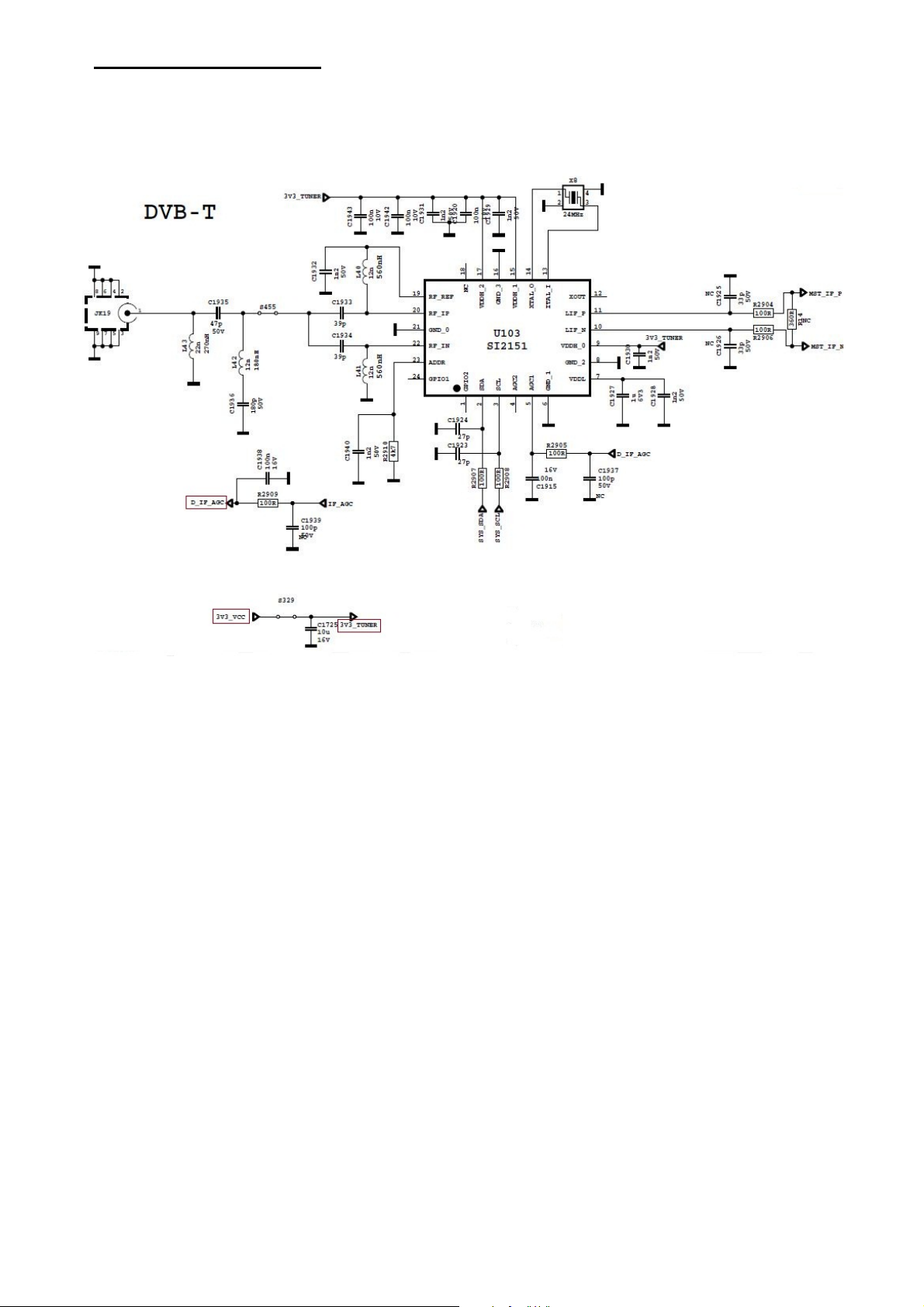
Problem: No signal in DVB-T/T2/C mode.
Check tuner supply voltage; 3V3_TUNER. Check tuner options are correctly set in Service menu. Check AGC
voltage at IF_AGC pin of tuner.
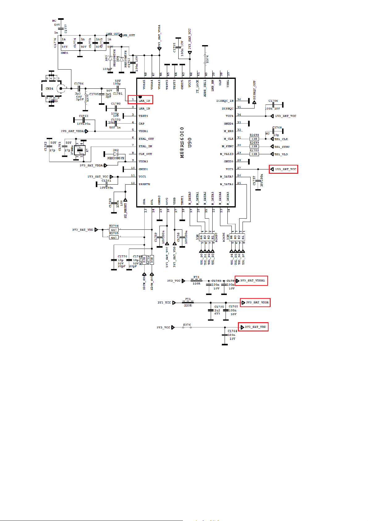
Problem: No signal or Low signal in DVB-S/S2 mode.
Check signal cables and LNB voltage, if there is no problem, check RS6000 supply voltages;
3V3_SAT_VDDA1, 3V3_SAT_VDDA, 3V3_SAT_VDD and 1V3_SAT_VCC.
If the above measurements are OK, then measure the voltage from the PIN1 of U90.
If the PIN1 voltage is equal to 0V, please check i2c waveforms and software. If the PIN1 voltage is lower than
1V(e.g: 0.8Vor 0.3V), change the U90 with a new part.
46
Page 48
47
Page 49
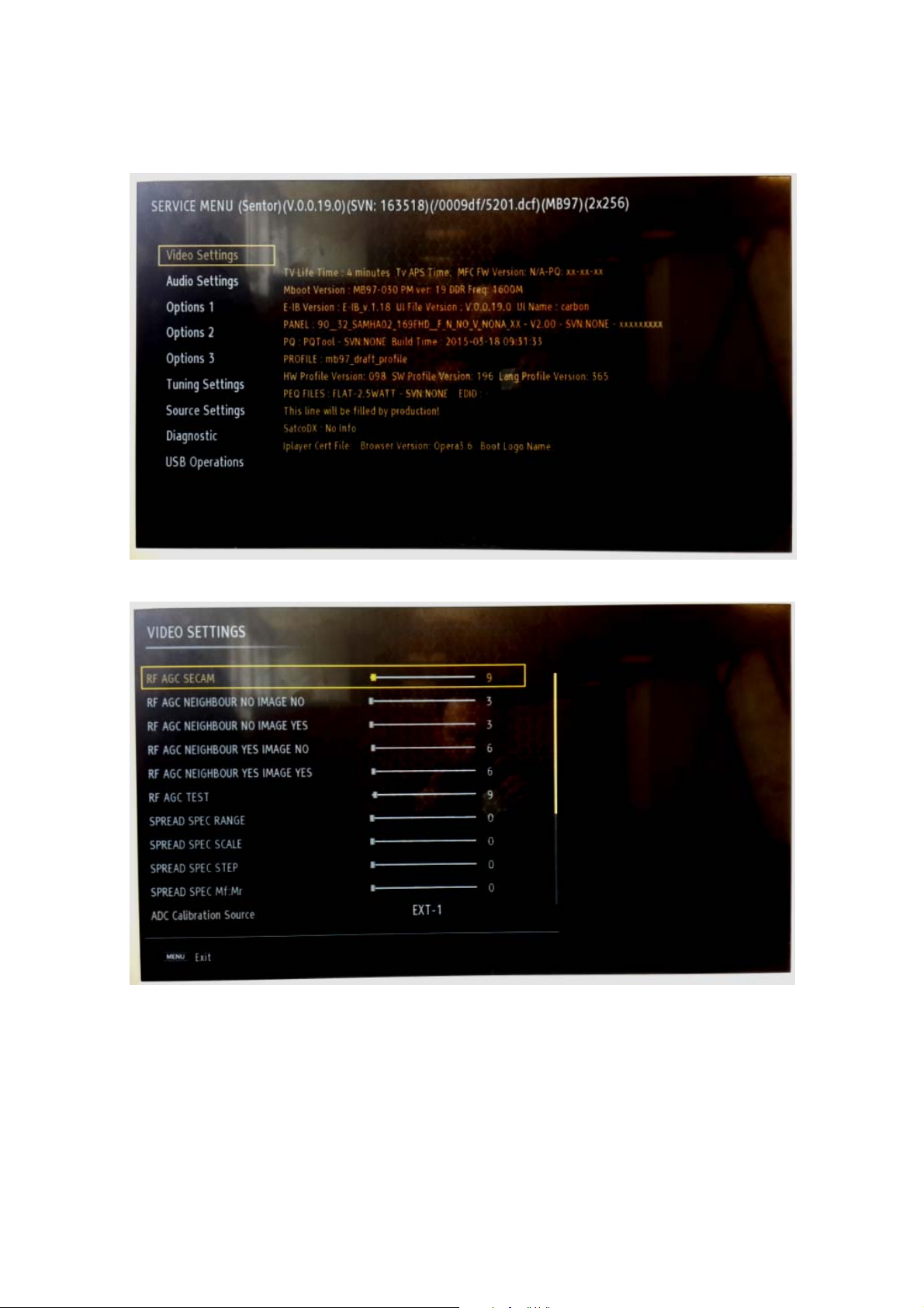
14. SERVICE MENU SETTINGS
In order to reach service menu, first Press “MENU” buton, then write “4725” by uisng remote controller.
You can see the service menu main screen below. You can check SW releases by using this menu. In addition,
you can make changes on video, audio etc. by using video settings, audio settings titles.
Service Menu Main Screen
48
Video Settings
Page 50
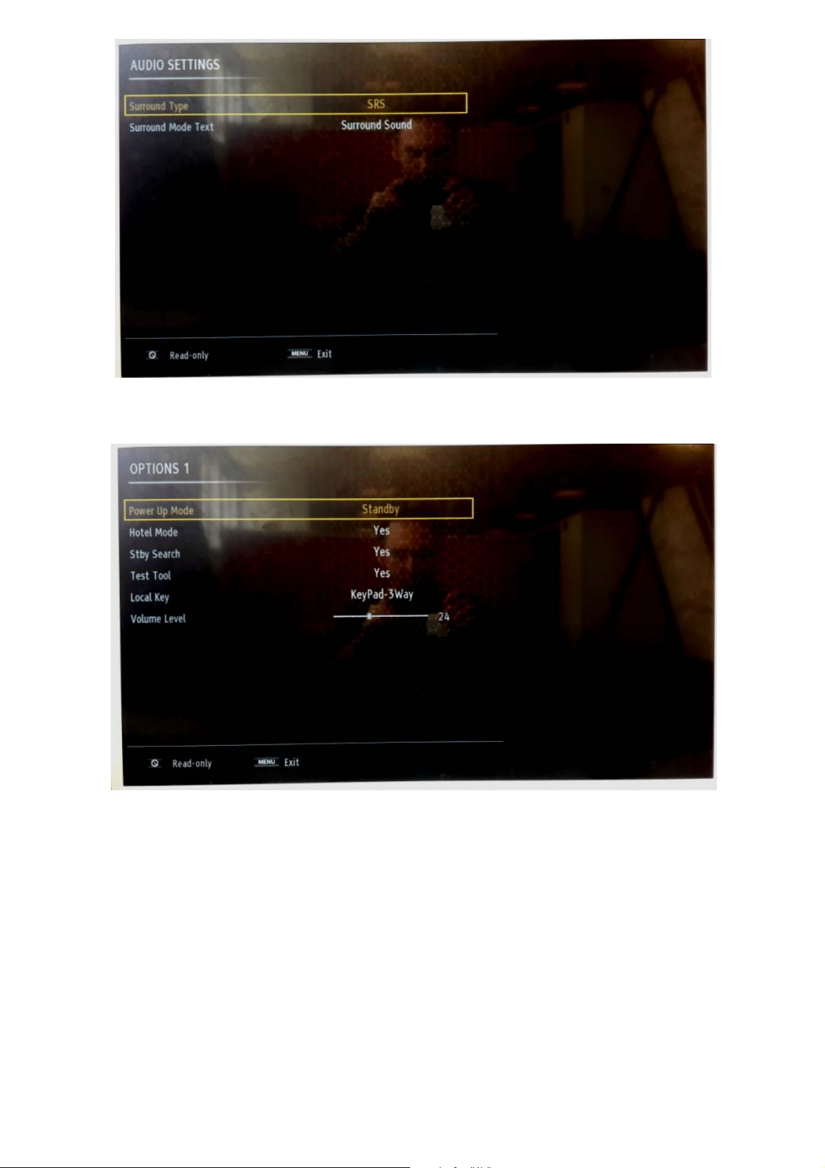
Audio Settings
49
Options-1 Menu
Page 51
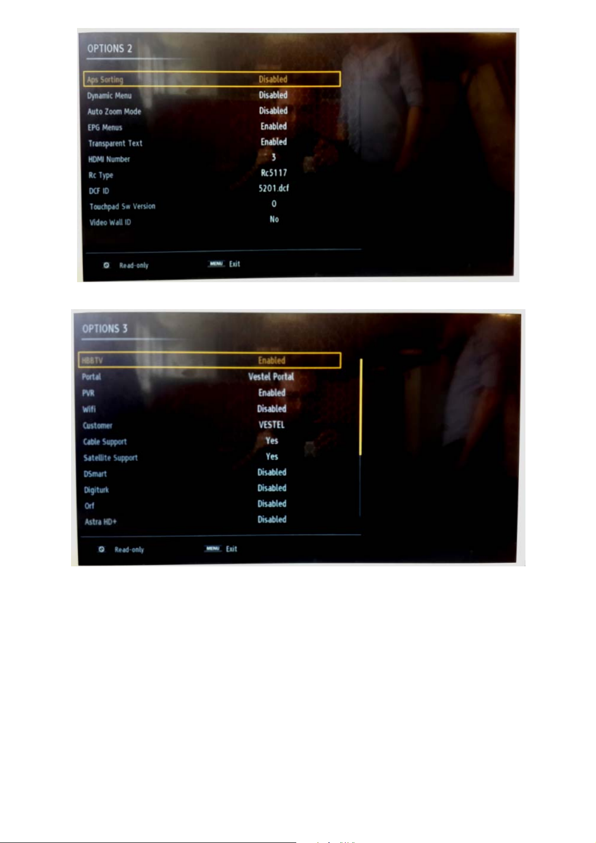
Options-2 Menu
50
Options-3 Menu
Page 52
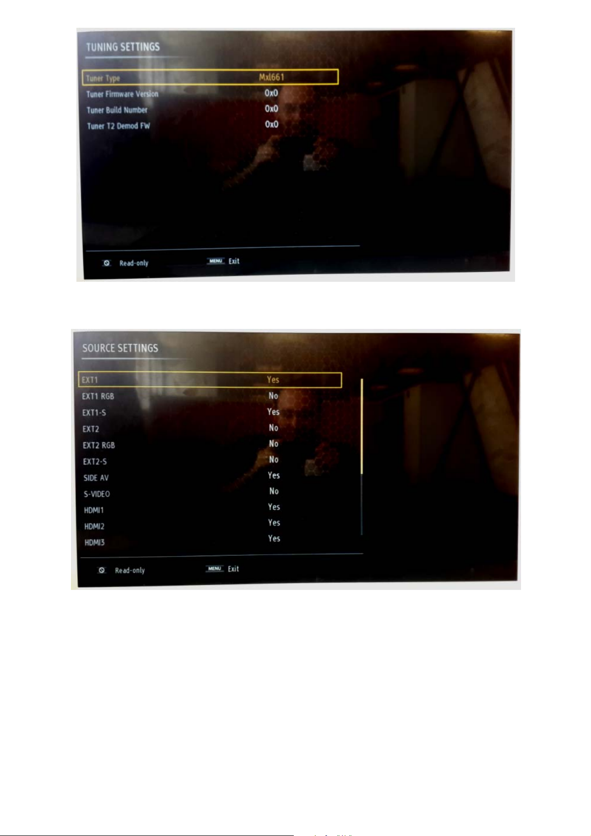
Tuner Settings Menu
51
Source Settings Menu
Page 53
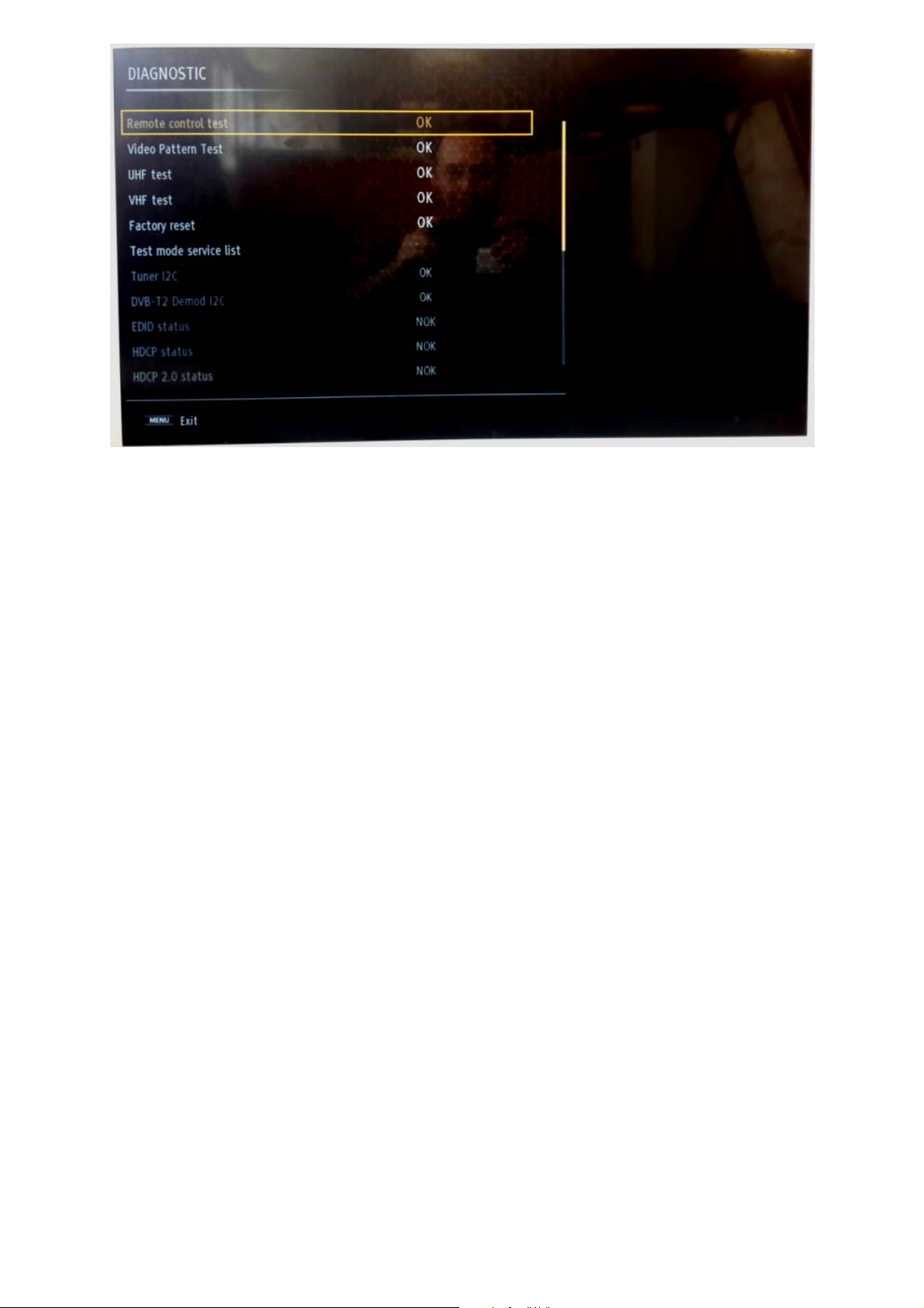
Diagnostic Menu
52
Page 54
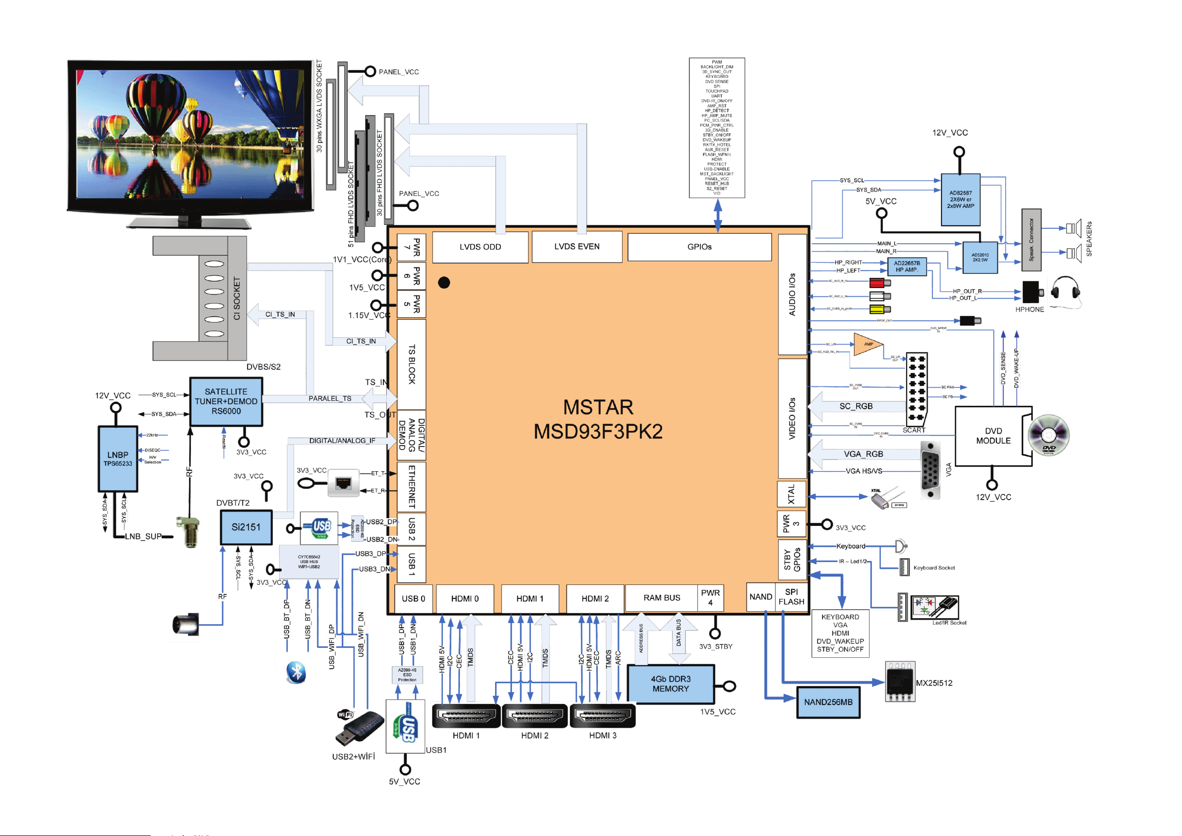
15. GENERAL BLOCK DIAGRAM
53
Page 55
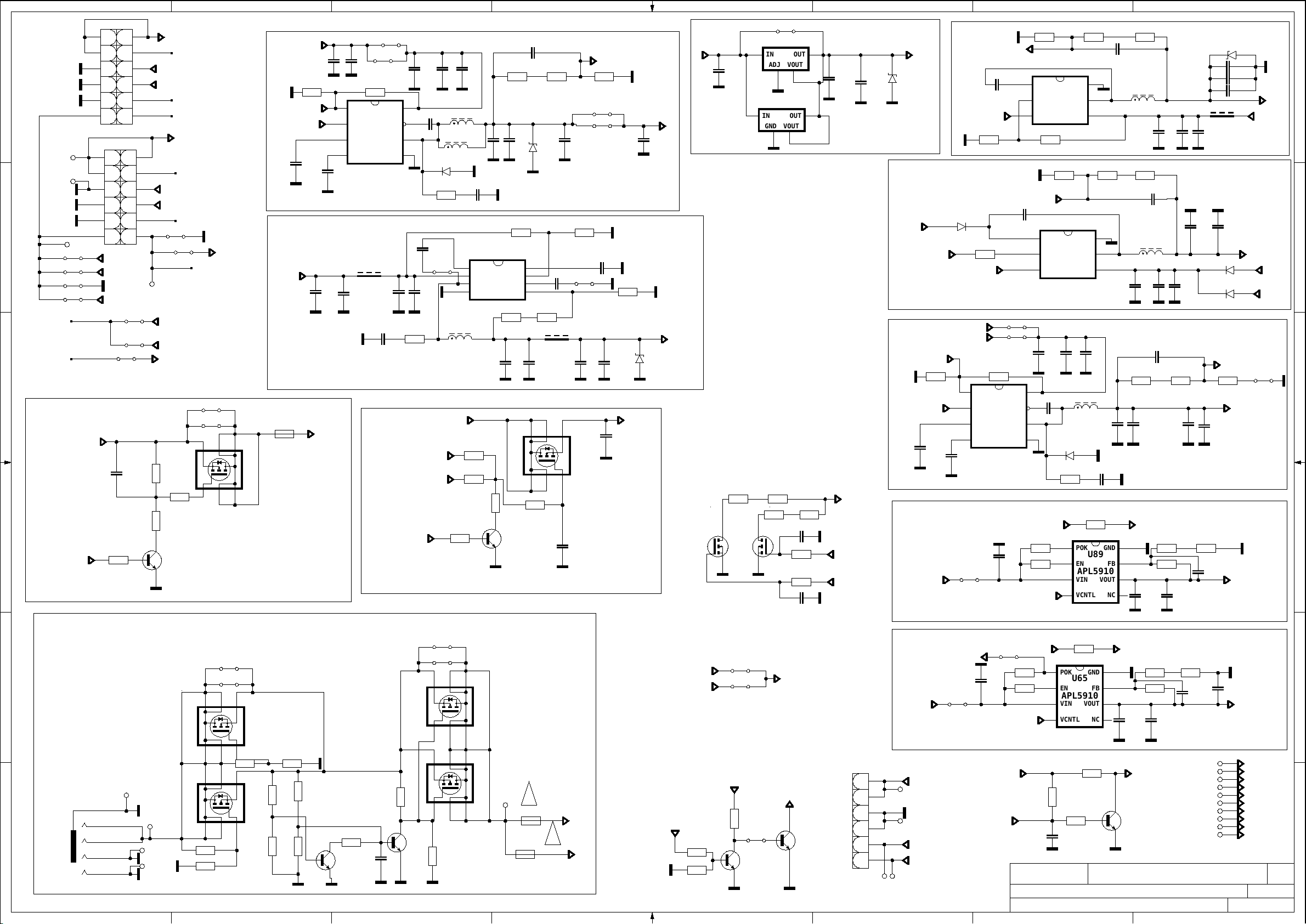
1 2 3 4 5 6 7 8
CN12
10u
10u
10V
VREG5
R2576
R2468
120k
6V3
22u
C1571
R2342
1 2
10k
SS
EN
VFB
10R
50V
33p
D49
8
7
6
5
C1364
10u
10V
C1578
R2
C1598
R2577
4k7
R2
R2510
C5V6
330R
4k7
C1544
16V
100n
5V_STBY
R2345
10k
C1424
100n 10V
S259
6V3470n
R2578=6.8K (30022069)
R2577= 22K(30022140)
R2576=470R (30022003)
F30
C1363
10u
10V
VFB
R2469
22k
S346
S138
12
10u
10V
R1
21
C1361
C1360
R2578
1k8
R1
D51
5V_STBY
10u
10V
C5V6
3V3_VCC
5V_STBY
C1365
10u
10V
12 11
10 9
8 7
A
6 5
4 3
2 1
CN11
1
TP75
TP76
B
1
TP178
S390
S391
S392
S393
power_pin3
power_pin9
1
2 1
4 3
6 5
8 7
10 9
12 11
3D_EN
3D_ENABLE
3D_BOOST
S262
S261
S254
12V_STBY
power_pin9
DIMMING
BACKLIGHT_ON/OFF
power_pin3
power_pin1
12V_STBY
power_pin9
DIMMING
BACKLIGHT_ON/OFF
power_pin3
S258
S342
power_pin1
1
TP77
STBY_ON/OFF
STBY_ON/OFF_NOT
5V_STBY
24V_VCC_AU
TPS_ENABLE
C1567
12V_VCC
12V_STBY
R2339
10k
VFB
1u
16V
10u 16V
C1550
100n 16V
12
C1452
C1445
1
2
3
4
8n2
C1391
25V220n
50V
C1443
16V10u
R2340
1 2
10k
EN
U63
VFB
TPS54528
VREG5
VSS
F20
60R
C1572
3n3 50V
S345
S341
VIN
VBST
SSW
GND
C1392
220n
25V
C1546
16V
8
7
6
5
R2542
C1545
100n
C1543 16V
100n
C1616
2
1
10n
16V
C1446
10u
16V
3R3
16V
SK24
R2543
S264
100n
D98
3R3
10u
L28
10u
L29
10u
L44
C1444
10u
16V
C1573
3n3
1
2
3
4
10V
C1357
50V
U70
TPS54329E
VBST
VIN
SW
GND
C1358
3V3_VCC STEP-DOWN
C
S343
12V_VCC SWITCH
12V_STBY
25V
220n
12
12
33k
R2268
12
33k
R2269
R2280
1 2
Q33
BC848B
21
C1390
D
MOSFET_CONTROL
R2338
10k
47R
S344
3 4
FS3
6
FDC642P
1
7A/32VDC
Q44
5
2
12V_VCC
STBY_ON/OFF_NOT
5V_STBY
12V_STBY
12V_VCC
R2337
10k
R2270
33k
R2267
33k
12
12
12
R2287
1k
Q32
BC848B
Q56
NTGS3446
R2279
1 2
47R
6
5
2
1
C1359
43
C1548100n
16V
10u
10V
5V_VCC
Q67
2N7002
R2893
680k
Q66
2N7002
5V_VCC SWITCH
S340
U94
LM1117
IN OUT
VOUT
ADJ
1234
U97
LM1117
3 2
GND
1
R430
56k
R2894
470k
OUTIN
VOUT
C1869
C1868
100n
4
R431
10V100n
R2837
1k
R2838
1k
3V3_STBY LDO
C1362
C1800
10u
10u 10V
10V
VFB_1V_CPU
1M
VID0
VID1
10V
VFB_1V5_VCC
3V3_STBY
D50
C5V6
C1825
VFB_1V5_VCC
R2821
4k7
3V3_WOWL
5V_STBY D92
1N4148
WIFI&BT/WOWL_EN
CORE_RESET
10k
R2840
VFB_1V_CPU
C1858
1u
16V
C1900
3V3_VCC
1V3_VCC_SAT LDO
R2843
1 2
10k
VFB_3V3WOWL
12V_VCC
12V_STBY
12
1
EN
2
VFB
TPS54528
3
VREG5
4
VSS
50V
8n2
C1750
S379
R2841
1 2
10k
U102
16V100n
VFB_3V3WOWL
C1826
100n 16V
S456
S457
100n
VIN
VBST
SSW
GND
10u
10V
R2
100k
R684
6
BOOT
5
EN
RT6213BHGJ6F
4
FB
R2842
1 2
10k
6
BOOT
5
EN
RT6213BHGJ6F
4
FB
RT6212
C1845
16V
8
C1843
7
100n
6
5
3V3_VCC
R2707
nc
4k7
R2706
nc
4k7
5V_VCC
R2839
GND
U100
LX
VIN
RT6212
R2892
12k
R2
GND
U101
LX
VIN
C1896
10u
16V
L36
16V
1u5
D99
SK24
R2884
3R3
R2709
12
1
POK
12
2
EN
APL5910
3
VIN
4 5
47k
1
2
3
33k
C1895
10u
16V
C1829
10u
C1872
47R
U89
50V
2p
R2891
37k4
1
2
3
10V
3n3
50V
GND
FB
VOUT
NCVCNTL
R2895
R1
C1893
NC
51k
L37
1V5_VCC
C5V6
10u
10u
10u
3u3
C1909
C1910
R2890
100R
R1
C1894 2p
NC
C1846
4k7
100n
16V
50V
16V
22u
16V
22u
C1834
10u
L38
10V
3u3
C1847
100n
16V
R2885
120k
6V322u
C1897
10u
16V
50V
33p
C1878
C1899
C1898
10u
16V
R2820
4k7
R2
100n
C1844
C1830
16V
10u
10V
CORE STEP-DOWN
1V3_SAT_VCC
C1748
10u
10V
R2703
22k
12k
R2708
8
7
6
C1749
10u
10V
R2695
R2
1k
C1767
R1
100n 10V
R2473=27K 30022137
R2290= 330R 30073653
D90
C1831
10V
C1832
10V
C1833
10V
F81
60R
C1835
10u
10V
1N5819
D97
1N5819
D96
VFB_1V_CPU
R2883
22k
R1
VDDC
1V3_SAT_VCC
1V5_VCC
12V_VCC
3V3_WOWL
12V_VCC
5V_STBY
S1
A
B
C
D
R2669
47R
1
POK
U65
2
EN
APL5910
3
VIN
4 5
10k
R2350
1 2
R2343
1 2
10k
21
16V
100n
C1551
GND
FB
VOUT
NCVCNTL
R2344
1 2
10k
8
7
6
2
PROJECT NAME :
POWER
<YOUR NAME HERE>
1V15_VCC
C1373
10u 10u
10V
STBY_ON/OFF_NOT
3
Q36
BC848B
1
R2473
R2617
22k
12k
C1372
10V
R2290
R2
R1
17mb110-r2
1k
C1426
100n
10V
C1370
10u
10V
1V15_VCC
R2473=27K 30022137
R2290= 330R 30073653
1
TP68
1
TP67
1
TP74
1
TP73
1
TP84
1
TP72
1
TP83
1
TP91
TP176
TP177
13-10-2015_18:11
87654321
5V_STBY
3V3_STBY
12V_VCC
5V_VCC
3V3_VCC
1V5_VCC
VDDC
1V15_VCC
3V3_WOWL
1V3_SAT_VCC
A3
T. SHT:
9
E
F
AX M
10k
Q35
BC848B
S255
S256
3 4
3 4
22k
R2687
3V3_VCC
C1371
10u
10V
S364
R2513
4k7
R2514
4k7
5V_VCC
nc
12
nc
12
STBY_ON/OFF
5
6
Q45
FDC642P
1
2
STBY_ON/OFF_NOT
S263
S253
MOSFET_CONTROL
3V3_VCC
1V15_POK
S268
1V15_VCC LDO
5
6
Q48
FDC642P
1
2
TP80
FS2
7A/32VDC
FS1
7A/32VDC
12V_STBY
12V_INV
5V_STBY
10k
R2744
39k
R2762
3V3_VCC
10k
R2743
S384
Q60
BC848B
TPS_ENABLE
Q59
BC848B
CN4
1 12V_INV
2
3
4
5
6
TP88
TP86
DIMMING
BACKLIGHT_ON/OFF
TP87
TP82
3V3_STBY
STBY_ON/OFF
VESTEL
SCH NAME :
ADAPTER PROTECTION
S265
6
FDC642P
1
6
FDC642P
1
R2349
1 2
10k
R2348
1 2
10k
S257
5
2
5
2
3 4
R2347
1 2
10k
3 4
22k
R2471
1k2
R2547
R2346
1 2
10k
R2470
R2544
22k
2k2
R2288
1 2
1k
Q34
BC848B
C1393
220n
10V
12
R2341
E
Q47
TP70
5
4
F
JK13
3
2
TP85
TP79
TP78
1
Q46
DRAWN BY :
Page 56
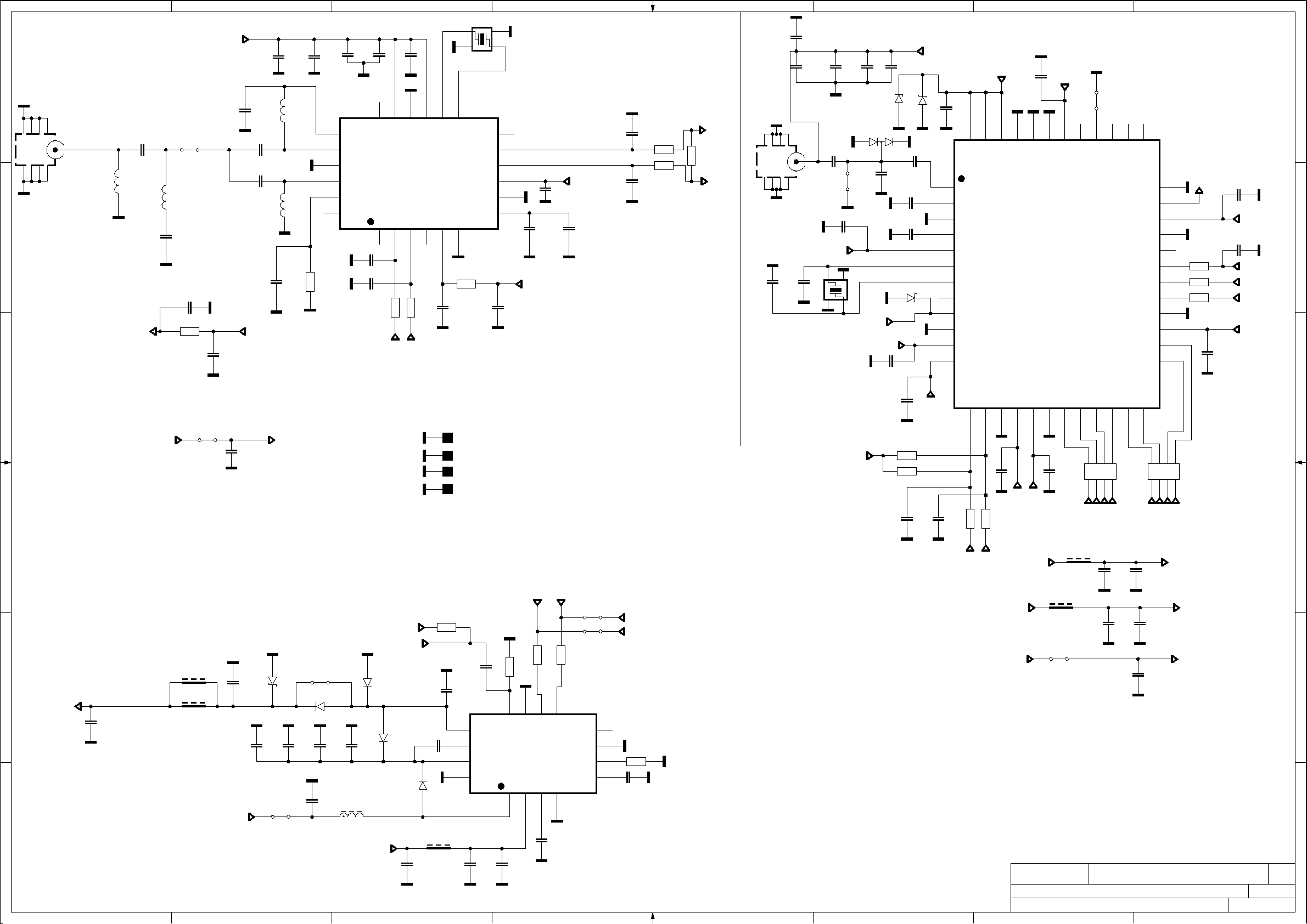
1 2 3 4 5 6 7 8
CN34
657498
GND1
C1782
50V
27p
NC
50V
1n
C1776
3 2
C1777
1n
50V
GND1
3V3_SAT_VDDA1
C1783
1
50V
27p
C1786
1n
50V
C1774
3p3 50V
2p2F
10V
3
27MHz
2
3V3_SAT_VDDA1
C1773
12
C1785
S375
C1763
100n
41
X7
1V3_SAT_VCC
1n
50V
BAV99
2pF
C1775
100pF
D1
50V
0p5
10V
1n
50V
D83
PESD9N5VH
C1781
100p
C1780
C1772
10nF
1n 50V
D82
PESD9N5VH
C1761
100n
LNB_OUT
D84
50V
50V100p
10V100n
C1753
PESD9N5VH
1
LNA_IP
2
LNA_IN
3
TEST0
4
CAP
5
VDDA1
6
XTAL_OUT
7
XTAL_IN
8
CLK_OUT
9
VDDA2
10
GNDD1
11
VCC1
12
RESETN
48
VDDA5
3V3_SAT_VDDA
47
46
VDDA3
VDDA4
45
TEST2
1V3_SAT_VCC
C1755
100n 10V
44
43
42
VCC5
GNDD5
TEST3
U90
M88RS6000
12
41
40
IT_LOCK
ADDR_SEL1
S374
39
38
OLF
LNB_EN
DISEQC_IN
DISEQC
M_SYNC
M_VALID
M_DATA7
M_DATA6
DVB-S
I2C: D2, D3 LOW
37
VSEL
36
35
34
VCC4
33
GNDD4
32
M_ERR
31
M_CLK
30
29
28
GNDD3
27
VCC3
26
25
D6, D7 High
DISEQC_OUT
C1756
100n
10V
1V3_SAT_VCC
C1768
50V
NC
R2698
33R
R2699
33R
R2700
33R
C1757
10p
TS0_CLK
TS0_SYNC
TS0_VLD
1V3_SAT_VCC
100n
10V
A
B
X8
2
24MHz
41
3
DVB-T
3V3_TUNER
C1943
10V
100n
C1942
10V
100n
C1931
50V
1n2
C1920
10V
100n
C1929
1n2
50V
A
18
17
16
15
14
VDDH_1
AGC2
4
XTAL_O
AGC1
5
100n
C1915
13
XTAL_I
GND_1
6
R2905
100R
16V
XOUT
LIF_P
LIF_N
VDDH_0
GND_2
VDDL
12
11
10
9
8
7
C1937
100p
50V
NC
C1930
C1927
D_IF_AGC
3V3_TUNER
1n2
6V3
1u
50V
C1928
1n2
50V
360R
NC
R14
MST_IF_P
MST_IF_N
NC
NC
C1925
C1926
33p
33p
50V
R2904
100RJK19
100R
R2906
50V
L40L41
50V
1n2
C1939
100p
50V
NC
C1932
C1933
39p
C1934
39p
IF_AGC
24
1
5 36789
B
L43
22n
D_IF_AGC
C1935
47p
50V
270nH
L42
C1936
12n
180p
S455
180nH
50V
C1938
R2909
100R
16V
100n
C1940
12n
12n
1n2
560nH560nH
50V
R2910
4k7
C1924
27p
C1923
27p
NC
GPIO2
1
VDDH_2
U103
SI2151
SDA
2
100R
R2907
SYS_SDA
GND_3
SCL
3
100R
R2908
SYS_SCL
19
RF_REF
20
RF_IP
21
GND_0
22
RF_IN
23
ADDR
24
GPIO1
C
S329
3V3_VCC
C1725
10u
16V
3V3_TUNER
GS1
GS2
GS3
GS4
3V3_SAT_VDD
D
SYS_SCL
SYS_SDA
100R
R2574
9
FAULT
EN/ADDR
SCL/VADJ
AGND
4
S442
S443
ISEL
TCAP
I2C: 0x60 LOW, 0x61 HIGH
R2538
D60
NC
C1450
10u
16V
NC
C1641
C1436
100n
4k7
50V
10V
1N5819
F42
1k
220n
100nF
13
14
15
16
C1438
100n
10V
VLNB
VCP
BOOST
PGND
C1451
10u
16V
100R
10k
R2386
12
11
10
SDA
EXTM
VCTRL
U71
TPS65233
VCC
VIN
LX
1
2
3
C1564
100n
16V
R2575
C1569
1u
16V
3V3_VCC
DISEQC_OUT
F44
E
LNB_OUT
LNB_OUT
C1638
10u
25V
1k
F43
1k
12V_VCC
C1636
10u
25V
C22V
C1635
10u
25V
S347
D73
C1634
10u
25V
S348
NC
D64
1N5819
C1633
10u
25V
C1632
10u
25V
L31
10u
C1640
2u2
25V
1N5819
D63
1N5819
D62
F
12V_VCC
3V3_STBY
3V3_STBY
8
7
R2236
6
130k
100k
C1437
22nF
5
10V
100n
C1760
R2704
1 2
4k7
R2705
1 2
4k7
C1770
50V
10p
100n
10V
20pF
S2_RESET
20pF
C1769
10p
50V
SDA
13
33R
R2701
SYS_SDA
VCC2
GNDD2
SCL
14
15
16
C1759
100n 10V
33R
R2702
1V3_SAT_VCC
3V3_VCC
SYS_SCL
3V3_VCC
3V3_VCC
VESTEL
SCH NAME :
DRAWN BY :
M_DATA1
M_DATA0
TEST1
VDDD
17
18
19
20
33R
10V 100n
C1758
3V3_SAT_VDD
F70
220R
F71
220R
S376
TUNER_SAT_LNB
<YOUR NAME HERE>
M_DATA5
M_DATA4
M_DATA3
M_DATA2
21
22
23
24
321
R4R3R2
5 4
TS0_D0
TS0_D1
R1
876
TS0_D2
TS0_D3
C1793
100n
10V
C1795
2u2
6V3
R2697
33R
R2696
C1794
100n
10V
C1765
100n
C1764
100n
10V
R4R3R2
10V
PROJECT NAME :
321
R1
876
5 4
TS0_D5
TS0_D6
TS0_D7
TS0_D4
3V3_SAT_VDDA1
3V3_SAT_VDDA
3V3_SAT_VDD
17mb110-r2
T. SHT:
13-10-2015_18:11
87654321
C
D
E
F
A3
9
AX M
Page 57
1 2 3 4 5 6 7 8
8
7
6
54
8
7
6
2
54
3
R2558
1 2
100R
C1689
D66
CDA4C16GTH
75R
R2611
C1583
50V
33p
75R
R2607
F55
50V4n7
12
SC_B
100n 10V
12
1k
SC_AUD_R_OUT
12
R2610
C1579
50V 33p
SC_R
R2362
10k
C1427
2 1
R2559
1 2
100R
C1688
4n7
50V
SC_CVBS-IN_pin20
12
C1582
33p
75R
75R
50V
R2918
Close to Chip side
SC_CVBS_OUT
C1580
50V33p
47R
12
50V
D79
C15V
SC_FB
UART-TX
SC_G
UART-RX
SC_PIN8
R2281
R2637
C1581
33p
R2638
5k1
2.7k
75R
75R
R2606
SC_AUD_L_OUT
INDIA OPTION
SCART_AUD_L_IN
SCART_AUD_R_IN
SC_CVBS-IN
4
YEL
3
WHT
2
RED
1
JK14
SCART
D67
A
B
SC1
C
21
TP94
20
SC_CVBS-IN_pin20
19
18
17
16
15
14
13
12
11
SCART LT1
10
9
8
7
TP98
6
5
4
3
2
1
TP102
TP93
TP92
TP100
TP101
TP99
S277
TP95
1
TP156
S274
TP96
TP157
TP97
S275
C1691
330p
50V
C1690
330p
50V
3
2
S276
75R
1 2
R2609
R2608
75R
12
1
C1796
33p
50V
SCART_AUD_L_IN
SCART_AUD_R_IN
F56
1k
5V_VCC
8
7
6
2
3
1 2
1 2
S278
54
CDA4C16GTH
R2355
1 2
S279
12
2k2
R2545
Close to MST IC
Close to MST IC
10k
R2356
1 2
12
2k2
R2546
10k
C1428
10k
R2357
1 2
nc
Close to MST IC
R2561
560R
R2562
1 2
100R
R2563
1 2
100R
R2560
560R
Close to MST IC
100n
10V
D75
2
1
BAV70
VGA_DDC_5V
VGA_VSNC
PC_SCL
PC_SDA
VGA_HSNC
D
VGA CONNECTOR
15
14
13
12
11
10
E
9
8
D68
1
1
TP110
TP1051TP1041TP103
1
TP158
1
VGA_DDC_5V
7
6
5
4
3
2
1
CN23
F
TP107
TP109
TP108
1 2
S282
1 2
S281
1 2
S280
321
5
4
D76
NUP4004M5
12
75R
R2612
12
75R
R2613
12
75R
R2614
VGA_B
VGA_G
VGA_R
SCART AUDIO FILTER
SCART_AUD_L_IN
SCART_AUD_R_IN
R2354
10k
10k
R2353
12k
R2618
12k
R2619
SAV Slim INPUT
WHT
RED
1
2
3
4
5
JK18
C1631
10u
25V
S403
S400
S397
S395
1
2
6
3
4
5
7
S398
S396
SAV_OPT1
R2359
10k
10k
R2358
!
FS4
4A/24VDC
FS5
4A/24VDC
SAV_CVBS
SAV_L
SAV_OPT2
SAV_R
12k
R2620
SAV_OPT2
S394
F80
1k
S446
F79
1k
SAV_OPT1
SAV_R
SAV_L
SAV_R
12k
R2621
DVD_Power
YEL
JK15
SAV AUDIO FILTER
SAV_AUD_L_IN
SAV_AUD_R_IN
Close to FS
12V_VCC
5V_VCC
DVD CONNECTION
DVD_CVBS
R2567
1 2
C1432
100R
12
4k7
R2518
DVD_SPDIF
DVD_SENSE
21
10V
100n
C1726
560p
50V
TP114
TP113
C1729
560p
50V
SAV_CVBS
SAV_L
D56
C5V6
C1681
220p
SC_AUD_L_IN
SC_AUD_R_IN
C1727
560p
50V
75R
R2615
1 2
C1677
D54
C5V6
SAV_L
F58
TP112
1k
F57
TP111
1k
SAV_R
SAV_L_IN
SAV_R_IN
C1728
560p
50V
IR_RC
DVD_IR_ON/OFF
R2455
NC
75R
R2639
180R
TP123
TP124
TP127
50V
R2566
1 2
100R
21
220p
C1575
BC848B
75R
R2919
50V
1 2
3n3
50V
C1574
50V3n3
1
Q39
2
47k
R2458
1 2
TP122
50V220p
C1680
3
1 2
CN24
21
43
65
87
109
SAV_CVBS
SAV_AUD_L_IN
SAV_AUD_R_IN
DVD_IR
R2520
12
4k7
N.C.
S287
C1449
10u
16V
1 2
S286
21
50V 27p
VGA_R
VGA_G
VGA_B
SC_R
SC_G
SC_B
12
4k7
R2519
TP125
C1698
12
R2911
75R
3V3_VCC
3V3_STBY
TP121
1
N.C.
1 2
S288
DVD_IR
TP126
HP_OUT_L
HP_OUT_R
12
R291212R2913
75R
75R
R2887
68R
33R
R2785
D77
C18V
DVD_Power
68R
SC_PIN8
DVD_WAKEUP
SLIM HEADPHONE OUTPUT
S285
S284
HP_DETECT
3V3_VCC
R2596
68R
33k
RIN0P
GIN0M
GIN0P
BIN0P
HSYNC0
VSYNC0
RIN1P
GIN1M
GIN1P
BIN1P
RIN2P
GIN2M
GIN2P
BIN2P
VSYNC2
HSYNC2
R2644
220R
SPDIF_COAX
TP119
10k
R2361
1 2
U95
MSD-G7
FB1
C1694
50V22p
S283
R2886
R2782
33R
R2783
R2784
SC_FB
R2780
33R
33R
33R
C1886
R2283
R2285
47R
47R
47R
47R
R2284
R2282
NC NC
SCART CVBS OUTPUT
SC_CVBS_OUT
R2272
C187947n
R2
C1882 47n
C1884
47n
16V
16V
JK16
16V
47n
S408
TP115
TP116
47n
16V
C1885
16V
16V
C188147n
16V
R1
R3
P1
R5
R4
U3
NC
U2
NC
T3
NC
T2
NC
V2
V3
U1
V1
T5
R7
1
2
3
1
1
C1880 47n
33R
R2781
VGA_HSNC
VGA_VSNC
C1883
47n
VESTEL
SCH NAME :
DRAWN BY :
C1619
10k
10n
R2360
16V
1 2
4k7
R2517
CVBS0_OUT
RN
RP
TN
TP
DM_P0
DP_P0
DM_P1
DP_P1
DM_P3
DP_P3
5
CVBS2P
CVBS1P
CVBS0P
VCOM0
CVBS_OUT1
VIN
3
VCC
2
GND
1
10V100n
C1430
220R
R2645
SCART_AV_INOUT
<YOUR NAME HERE>
21
50V
TP118
220p
C1678
TP117
C1679
R2565
100R
21
50V
220p
C1618
10n
16V
1
D55
A6
B6
B5
C5
AA11
AB11
AA12
AB12
AC10
AB10
N5
R6
P5
P4
P6
SPDIF_COAX
ET_RN
ET_RP
ET_TN
ET_TP
USB3_DN
USB3_DP
USB1_DN
USB1_DP
USB2_DN
USB2_DP
47n
C1888
C1889 47n
C1890 47n
16V
CVBS0_OUT
SPDIF OUT
C1431
100n
10V
Q38
BC848B
220R
R2646
PROJECT NAME :
1
2
6
3
4
JK17
5
7
TP120
3V6 lik zener kullanilmali
C5V6
R2889
33R
F59
1k
100R
75R
DVD_CVBS
SAV_CVBS
SC_CVBS-IN
5V_VCC
SPDIF_OUT
47n C1887
12
4k7
R2515
C1429
100n 10V
12
R2787
33R
68R
R2888
C1692
22p
50V
R2786
33R
R2788
R2564
C1693
4k7
R2516
22p
50V
17mb110-r2
T. SHT:
13-10-2015_20:53
87654321
A
B
C
D
E
F
A3
9
AX M
Page 58
1 2 3 4 5 6 7 8
R2846
1 2
10k
1
VSYNC_BS
3D_ENABLE
USB_ENABLE
BACKLIGHT_DIM
3D_SYNC_OUT
1 2
S411
HSYNC_BS
PWM_OUT_LED3
UART-RX
UART-TX
SYS_SCL
SYS_SDA
A
B
PC_SDA
PROTECT
C
AMP_RESET
VID0
VID1
MST_BACKLIGHT_ON/OFF
R2802
33R
R2806
33R
R2804
33R
33R
DVD_SENSE
3D_BOOST
FLASH-WPN1
KEYBOARD
AUX_RESET
SPI-SCK
SPI-SDI
SPI-SDO
SPI-CS1N
PC_SCL
1 2
TP180
TP181
DVD_IR_ON/OFF
R2805
33R
TOUCHPAD_SCL
STBY_ON/OFF
DVD_WAKEUP
TOUCHPAD_SDA
3V3_STBY
HDMI3_5V 33R
4k7
PCM_PWR_CTL
R2803
R2801
S412
R2797
33R
33R
R2798
AMP_MUTE
TX_HOTEL
LED1
RX_HOTEL
LED2
33R
1 2
10k
R2898
R2807
R2836
33R
R2896
PANEL_VCC_ON/OFF
D
R2675
3V3_VCC
10k
R2674
10k
VSYNC_BS
HSYNC_BS
12
12
SPI_SCL_BS
SPI_SDI_BS
SPI_SDO_BS
SPI_XCS_BS
R2672
3V3_VCC
E
1 2
LED2
LED1
TOUCHPAD_SCL
TOUCHPAD_SDA
DVD_WAKEUP
AMP_MUTE
SPI-SDO
UART-RX
UART-TX
F
PCM_PWR_CTL
PANEL_VCC_ON/OFF
USB_ENABLE
3D_BOOST
SYS_SCL
SYS_SDA
10k
1 2
10k
1 2
10k
1 2
10k
1 2
10k
1 2
10k
1 2
10k
1 2
10k
1 2
10k
1 2
10k
1 2
10k
1 2
10k
1 2
10k
4k7
4k7
R2854
R2847
R2848
R2849
R2852
R2853
R2855
R2850
R2851
R2857
R2859
R2860
R2858
12
R2536
12
R2535
3V3_VCC
3V3_VCC
10k
R2673
10k
3V3_STBY
3V3_STBY
3V3_STBY
3V3_STBY
3V3_STBY
3V3_STBY
3V3_STBY
3V3_STBY
3V3_STBY
3V3_VCC
3V3_VCC
3V3_VCC
3V3_VCC
12
12
10k
1
10k
G22
PWM0
H21
PWM1
H22
PWM2
L20
PWM3
J21
PWM4
D8
PWM_PM
C7
SAR0
F6
SAR1
D5
SAR2
B7
SAR3
D6
SAR4
C1
PM_SPI_CK
C3
PM_SPI_DI
B1
PM_SPI_D0
B2
SPI_CZ1/PM_GPIO[6]
E2
DDCA_CK/UART0_RX
D2
DDCA_DA/UART0_TX
L18
DDCR_CK
L19
DDCR_DA
J20
UART_RX2
K20
UART_TX2
D9
GPIO_PM0
D4
GPIO_PM1/PM_UART_TX
E7
GPIO_PM2
E10
GPIO_PM3
E6
GPIO_PM4
D3
GPIO_PM5/PM_UART_RX
C8
GPIO_PM7
D7
GPIO_PM8
D10
GPIO_PM11
G7
GPIO_PM12
E4
VID0
F7
VID1
W3
PCM2_IRQA_N/GPIO
AC6
PCM2_CD_N/GPIO
Y7
PCM2_CE_N/GPIO
K19
GPIO0
33R
33R
33R
33R
33R
33R
3V3_VCC
R2844
3V3_VCC
2
R2845
3V3_VCC
2
4
U95
MSD-G7
R2678
R2679
R2677
R2680
R2681
R2682
CN38
1
2
3
4
5
6
7
8
CHIP CONFIG
A0P
A0M
A1P
A1M
A2P
A2M
ACKP
ACKM
A3P
A3M
A4P
A4M
B0P
B0M
B1P
B1M
B2P
B2M
BCKP
BCKM
B3P
B3M
B4P
B4M
N22
P21
P22
R21
R22
R23
T21
T23
T22
U21
U22
V21
J22
J23
K21
K23
K22
L21
L22
M21
M22
M23
N21
N23
1 2
S414
1 2
S413
1 2
S416
1 2
S415
TX_1_4_P
TX_1_4_N
TX_1_3_P
TX_1_3_N
TX_1_CLK_P
TX_1_CLK_N
TX_1_2_P
TX_1_2_N
TX_1_1_P
TX_1_1_N
TX_1_0_P
TX_1_0_N
TX_2_4_P
TX_2_4_N
TX_2_3_P
TX_2_3_N
TX_2_CLK_P
TX_2_CLK_N
TX_2_2_P
TX_2_2_N
TX_2_1_P
TX_2_1_N
TX_2_0_P
TX_2_0_N
A_A[0]
A_A[1]
A_A[2]
A_A[3]
A_A[4]
A_A[5]
A_A[6]
A_A[7]
A_A[8]
A_A[9]
A_A[10]
A_A[11]
A_A[12]
A_A[13]
A_A[14]
A_CASZ
A_RASZ
A_WEZ
A_ODT
A_BA[0]
A_BA[1]
A_BA[2]
A_RET
A_CKE
A_DQL[0]
A_DQL[1]
A_DQL[2]
A_DQL[3]
A_DQL[4]
A_DQL[5]
A_DQL[6]
A_DQL[7]
A_DQU[0]
A_DQU[1]
A_DQU[2]
A_DQU[3]
A_DQU[4]
A_DQU[5]
A_DQU[6]
A_DQU[7]
A_DQML
A_DQMU
A_MCLK
A_MCLKZ
A_DQSL
A_DQSLB
A_DQSU
A_DQSUB
A_CA0
DDR
E13
B_DDR3_A0
F14
B_DDR3_A1
D12
B_DDR3_A2
B12
B_DDR3_A3
E17
B_DDR3_A4
B13
B_DDR3_A5
F16
B_DDR3_A6
C13
B_DDR3_A7
D16
B_DDR3_A8
A14
B_DDR3_A9
F18
B_DDR3_A10
D15
B_DDR3_A11
D17
B_DDR3_A12
C14
B_DDR3_A13
E15
B_DDR3_A14
B11
B_DDR3_CASZ
C10
B_DDR3_RASZ
D13
B_DDR3_WEZ
B10
B_DDR3_ODT
A11
B_DDR3_BA0
D18
B_DDR3_BA1
A12
B_DDR3_BA2
F12
B_DDR3_RESETB
E19
B_DDR3_CKE
A22
B_DDR3_DQ0
A18
B_DDR3_DQ1
C21
B_DDR3_DQ2
C17
B_DDR3_DQ3
C22
B_DDR3_DQ4
C16
B_DDR3_DQ5
B23
B_DDR3_DQ6
B17
B_DDR3_DQ7
F20
B_DDR3_DQ8
D21
B_DDR3_DQ9
D19
B_DDR3_DQ10
E23
B_DDR3_DQ11
E21
B_DDR3_DQ12
D22
B_DDR3_DQ13
D20
B_DDR3_DQ14
F22
B_DDR3_DQ15
C18
B_DDR3_DM0
D23
B_DDR3_DM1
C15
B_DDR3_MCLK
B15
B_DDR3_MCLKZ
A21
B_DDR3_DQS0
C20
B_DDR3_DQS0B
B20
B_DDR3_DQS1
C19
B_DDR3_DQS1B
D14
B_DDR3_CS0
MSD-G7
U11
A_DDR3_RST
U12
A_DDR3_CKE
R2602
1
U95
A_MCLK
A_MCLKZ
56R
56R
R2601
16V
10n
C1615
A_A[0]
A_A[1]
A_A[2]
A_A[3]
A_A[4]
A_A[5]
A_A[6]
A_A[7]
A_A[8]
A_A[9]
A_A[10]
A_A[11]
A_A[12]
A_A[13]
A_A[14]
A_BA[0]
A_BA[1]
A_BA[2]
A_CKE
A_CA0
A_RASZ
A_CASZ
A_WEZ
A_RET
R2604
240R
1V5_MIU0
1V5_MIU0
1V5_VCC
C1537
N3
A0
P7
A1
P3
N2
P8
P2
R8
R2
T8
R3
L7
R7
N7
T3
J1
L1
M7
L9
T7
J9
M2
N8
M3
J7
K7
K9
L2
J3
K3
L3
T2
L8
A2
A3
A4
A5
A6
A7
A8
A9
A10/AP
A11
A12/BC
A13
NC1
NC2
NC3
NC4
NC5
NC6
BA0
BA1
BA2
CK_0
CK_1
CKE
CS
RAS
CAS
WE
RESET
ZQ
VDD_1
A9B3E1G8J2J8M1M9P1P9T1T9B1B9D1D8E2E8F9G1G9
B2D9G7K2K8N1N9R1R9A1A8C1C9D2E9F1H2
1k
R2585
1k
R2584
C1526
C1527
100n 100n
16V
16V
C1356
10u
10V
close to DDR power pin
F15
60R
C174710u
100n
16V
10V
VESTEL
SCH NAME :
DRAWN BY :
VDD_5
VDD_4
VDD_3
VDD_2
H5TQ2G63BFR-PB
VSS_4
VSS_3
VSS_2
VSS_1
16V
C1518 100n
C1525
100n
16V
C1535
16V
C174610u
10V
DDR_GPIO_EMMC
<YOUR NAME HERE>
1V5_MIU0
VDD_9
VDD_8
VDD_7
VDD_6
U72
VSS_9
VSS_8
VSS_7
VSS_6
VSS_5
A-MVREFDQ
50V
1n C1644
C1524
16V
C1534
100n 100n
16V
1V5_MIU0
C1538
16V100n
PROJECT NAME :
VDDQ_2
VDDQ_1
VSS_11
VSS_10
1V5_MIU0
C1523
100n 100n
16V
C1533
100n
16V
VDDQ_4
VDDQ_3
VSS_12
VDDQ_6
VDDQ_5
VSSQ_2
VSSQ_1
R2587
C1522
16V
C1532
100n
16V
H9
VDDQ_9
VDDQ_8
VDDQ_7
VREF_DQ
VREF_CA
DQL0
DQL1
DQL2
DQL3
DQL4
DQL5
DQL6
DQL7
DQU0
DQU1
DQU2
DQU3
DQU4
DQU5
DQU6
DQU7
DQSL_0
DQSL_1
DQSU_1
DQSU_0
DML
DMU
ODT
VSSQ_8
VSSQ_7
VSSQ_6
VSSQ_5
VSSQ_4
VSSQ_3
1k
1k
R2586
C1521
100n 100n
16V
C1531
100n
16V
17mb110-r2
H1
M8
E3
F7
F2
F8
H3
H8
G2
H7
D7
C3
C8
C2
A7
A2
B8
A3
F3
G3
B7
C7
E7
D3
K1
VSSQ_9
16V
100n
C1536
100n
16V
C1530
100n
16V
13-10-2015_18:51
87654321
A-MVREFDQ
A-MVREFCA
A_DQL[0]
A_DQL[1]
A_DQL[2]
A_DQL[3]
A_DQL[4]
A_DQL[5]
A_DQL[6]
A_DQL[7]
A_DQU[0]
A_DQU[1]
A_DQU[2]
A_DQU[3]
A_DQU[4]
A_DQU[5]
A_DQU[6]
A_DQU[7]
A_DQSL
A_DQSLB
A_DQSUB
A_DQSU
A_DQML
A_DQMU
A_ODT
50V
1n
C1645
C1519C1520
100n
16V
C1529
100n
T. SHT:
A-MVREFCA
C1517
100n
16V
C1528
100n
16V16V
A3
9
A
B
C
D
E
F
AX M
Page 59
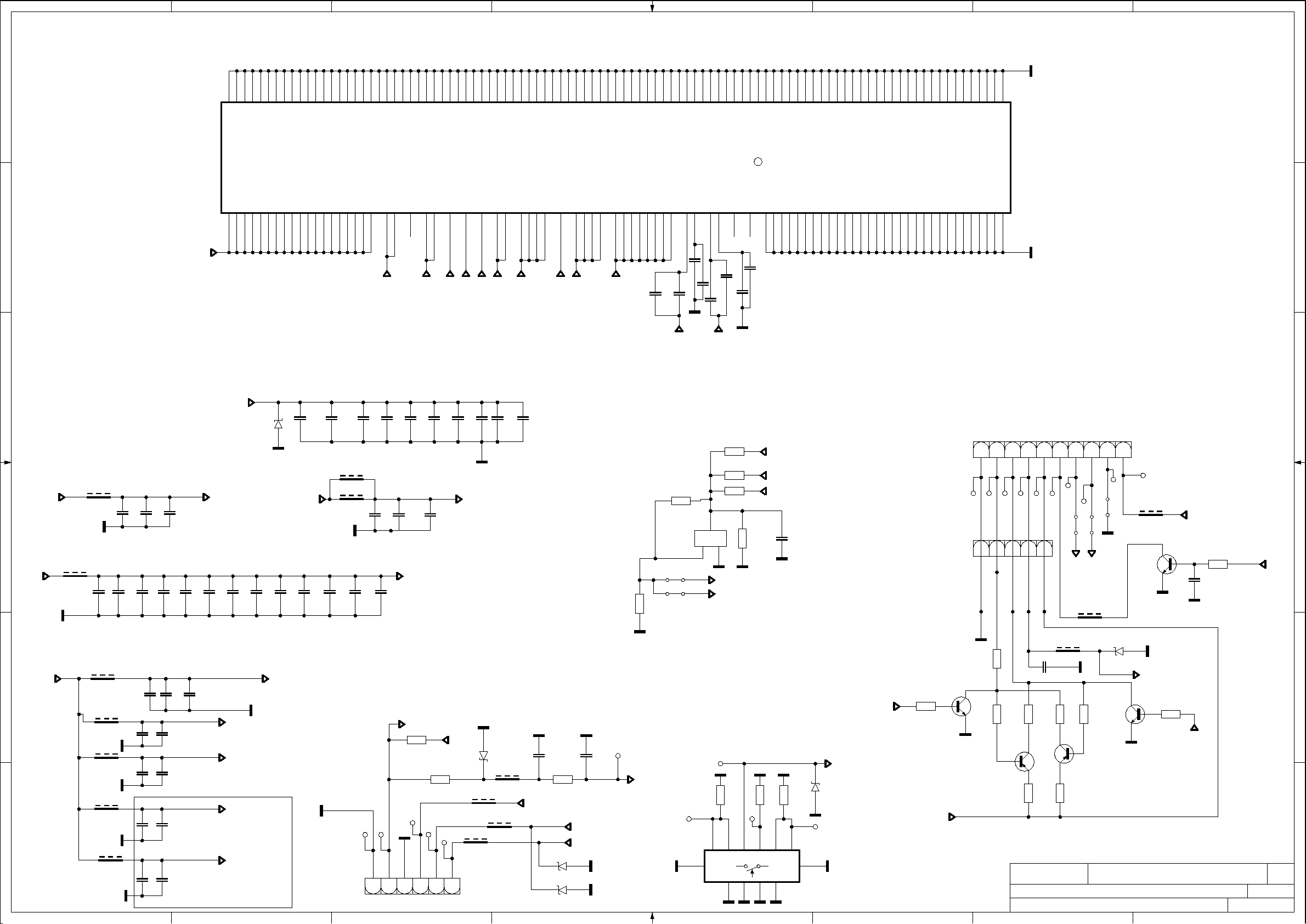
1 2 3 4 5 6 7 8
A
B
C
D
1V5_VCC
3V3_VCC
F72
60R
F54
1k
C1912
10u
6V3
C1602
10u
6V3
C1911
10u
6V3
C1507
100n
16V
C1605
10u
6V3
C1508
100n
16V
C1462
100n
16V
VDDC
C1461
100n
16V
NC
W_VDD33
C1460
100n
16V
NC
A20
GND_31
VDDC_0
G21
VDDC
C1459
100n
16V
B4
B14
GND_32
VDDC_1
M13
G23
B18
B16
GND_33
GND_34
VDDC_2
VDDC_3
M15
M14
C1458
100n
16V
B21
B19
GND_35
GND_36
VDDC_4
VDDC_5
M17
M16
C5V6
100n
C6
B22
GND_37
GND_38
GND_39
VDDC_6
VDDC_7
VDDC_8
N15
N14
D100
C1852
1V15_VCC
C1838
16V
C9
C11
GND_40
GND_41
VDDC_9
VDDC_10
N17
N16
4u7
6V3
C1839
100n
16V
D11
C23
C12
GND_42
GND_43
VDDC_11
VDDC_12
P15
P14
N19
C1840
100n
E8
E22
GND_44
GND_45
VDDC_13
VDDC_14
P17
P16
C1856
10u
6V3
F90
1k
F89
1k
16V
F9
F10
GND_46
GND_47
GND_48
VDDC_15
VDDC_16
VDDC_17
N18
P18
C1857
10u
6V3
C1841
100n
16V
F15
F13
F11
GND_49
GND_50
VDDC_18
T10
N20
C1867
C1604
10u
6V3
C1842
100n
16V
F21
F19
F17
GND_51
GND_52
GND_53
GND_54
MCP_VDD_0
MCP_VDD_1
NC/TESTPIN
L14
U10
MCP_VDDC
47u
470n
6V3
6V3
C1873
C1514
100n
16V
close to IC
AVDD_DDR
G8
F23
AC12
GND_55
GND_56
GND_57
DVDD_DDR_B
DVDD_DDR_A
N13
J12
VDDC
C1853
C1513
100n
16V
AA3
AB3
GND_58
GND_59
AVDDL_DVI
M12
VDDC
4u7
6V3
W7
Y10
GND_60
GND_61
MCP_VDD33
AA10
W_VDD33
4u7
6V3
C1854
MCP_VDDC
V6
V7
GND_62
GND_63
AVDD_AU33
U5
AVDD_AU
4u7
6V3
C1855
U17
U13
U14
U15
U16
GND_64
GND_65
GND_66
GND_67
GND_68
AVDD3P3_USB_0
AVDD3P3_USB_1
AVDD_NODIE
N7
V5
V4
VCC3V3_AG2
VCC3V3_AG1
C1837
C1494
100n
100n
16V
16V
U6
U7
U8
L11
GND_69
GND_70
GND_71
GND_72
AVDD3P3_ADC
AVDD3P3_DADC
AVDD3P3_ETH
N8
P7
N6
T15
T16
T17
T18
T19
T20
GND_73
GND_74
GND_75
GND_76
GND_77
AVDD3P3_DMPLL
AVDD_MOD_0
AVDD_MOD_1
VDDP/VDDP_3318
L7
L6
K8
K7
U4
VCC3V3_AG
AVDD_DMPLL
T12
T13
T14
GND_78
GND_79
GND_80
AVDD_PLL
AVDD_DDR1_0
A9
H13
AVDD_DDR
T8
T9
L16
T11
GND_81
GND_82
GND_83
GND_84
GND_85
AVDD_DDR1_1
AVDD_DDR1_2
AVDD_DDR0_0
AVDD_DDR0_1
AVDD_DDR0_2
P13
P12
H12
AB13
NC
6V3 470n
C1861
4k7
R2774
1 2
T6
T7
R19
R20
L15
GND_86
GND_87
GND_88
GND_89
VDDIO_DRAM_0
VDDIO_DRAM_1
AVDD04_DDR_A
R13
R12
AA13
AC13
6V3
C1860
6V3470n
C1859
AVDD_DDR
R2775
12
4k7
U86
MAX809LTR
1 2
S440
1 2
S441
R11
R15
R16
R17
R18
GND_90
GND_91
GND_92
GND_93
GND_94
AVDD11_DDR_A
AVDD04_DDR_B
AVDD11_DDR_B
C2
A8
B9
470n
NC
6V3
NC
470n
470n
C1865
6V3
6V3470n
C1862
C1866
AVDD_DDR
R2662
39k
R2664
15k
R2647
220R
3
VCC
GNDRST
2 1
AUX_RESET
CORE_RESET
P8
R8
R9
P10
P11
R10
GND_95
GND_96
GND_97
GND_98
GND_99
GND_100
6
U95
AVDD_5V_HDMI_D
VSENCE
GND_0
GND_1
G9
F8
G10
M18
NC
6V3 470n
C1863
470n
6V3
C1864
24V_VCC_AU
12V_VCC
5V_VCC
10k
R2381
N9
M10
N10
R14
GND_101
GND_102
GND_103
GND_104
MSD-G7
GND_2
GND_3
GND_4
GND_5
G15
G14
G13
G12
C1563
100n
16V
M8
M9
GND_105
GND_106
GND_107
GND_6
GND_7
GND_8
G17
G16
M6
M7
GND_108
GND_109
GND_9
GND_10
G19
G18
M4
M5
L13
GND_110
GND_111
GND_11
GND_12
H7
K4
G20
L9
L10
GND_112
GND_113
GND_114
GND_13
GND_14
GND_15
H9
H8
L4
L5
L8
GND_115
GND_116
GND_16
GND_17
H14
H11
H10
K14
K15
GND_117
GND_118
GND_119
GND_18
GND_19
GND_20
H16
H15
K10
K11
K13
GND_120
GND_121
GND_21
GND_22
H19
H18
H17
K9
J16
GND_122
GND_123
GND_124
GND_23
GND_24
GND_25
J7
H20
J13
J14
J15
GND_125
GND_126
GND_26
GND_27
A7
J9
J8
1
CN27
1
TP36
1
CN28
J10
J11
GND_127
GND_128
GND_129
GND_28
GND_29
GND_30
A17
A15
2
1
1
TP38
TP37
2
A
B
C
LED
3
4
5
6
7
8
9
10
TP155
F53
Q21
BC848B
TP154
1k
5V_STBY
D
3
2
1
C1643
1n
50V
R2307
1 2
10k
PWM_OUT_LED3
1
1
1
TP25
TP169
5
TP35
S226
TP34
1 2
S228
S227
1 2
1 2
TOUCHPAD_SDA
TOUCHPAD_SCL
1k
F52
TP39
3
4
E
F
3V3_STBY
F82
1k
F12
1k
F73
1k
F74
1k
F75
1k
100n
16V
C1913
C1820
C1821
100n
16V
C1822
100n
16V
C1823
100n
16V
4u7
6V3
100n
16V
C1875
4u7
6V3
C1914
C1473
C1491
100n
16V
C1477
NC
100n
16V
C1486
100n
16V
50V
100n
NC
NC
VCC3V3_AG1
VCC3V3_AG2
NC
AVDD_AU
Close to IC
AVDD_DMPLL
NC
VCC3V3_AG
TOUCH_PAD_OPTION
TP29
CN13
F51
1k
150R
R2654
R2309
KEYBOARD
KEYBOARD_ONBOARD
R2684
10k
TP164
TP30
3
2
1
R2276
1 2
47R
TP31
4
TP32
5
3V3_STBY
F50
1k
6
C5V6
F47
1k
10k
4
+
3
SW1
G4
3-WAY
2k
R2623
TP28
SOURCE
C
T
2
G3
G2
G1
KEYBOARD_ONBOARD
D43
C5V6
1 2
470R
R2655
-
TP27
1
E1
12
D42
F48
1k
F49
1k
C1421
2
100n
1
10V
3V3_STBY
R2277
1 2
47R
C1420
2
100n
1
10V
TOUCHPAD_SCL
TP189
TP33
KEYBOARD
R2306
TP26
TOUCHPAD_SDA
D46
C5V6
D45
E2
C5V6
LED2
1 2
10k
5V_STBY
3
Q23
2
BC848B
1
10k
1 2
R2311
Q53
BC858B
SCH NAME :
DRAWN BY :
C1697
21
27p
50V
220R
220R
R2643
1 2
R2640
1 2
Q52
BC858B
220R
220R
R2642
1 2
R2641
1 2
VESTEL
MAIN_IC_POWER
<YOUR NAME HERE>
D44
C5V6
IR_RC
3
Q24
10k
BC848B
1 2
R2310
1
PROJECT NAME :
R2308
2
1 2
10k
17mb110-r2
LED1
13-10-2015_18:11
87654321
A3
T. SHT:
E
F
9
AX M
Page 60
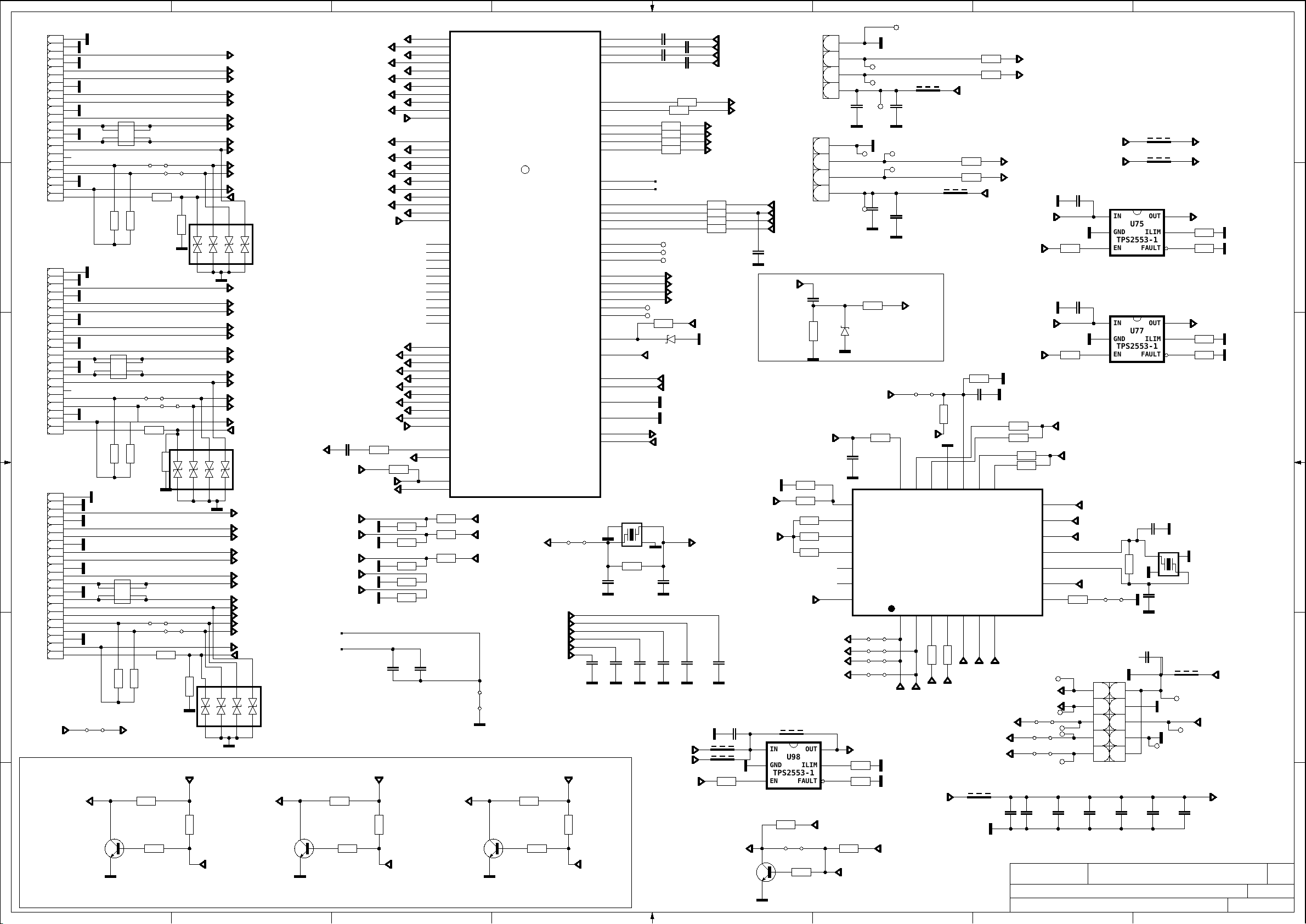
1 2 3 4 5 6 7 8
1
TP143
TP142
C1380
10u
10V
R2226
100k
S369
S368
S349
S350
1
C1381
10u
10V
TP138
1
TP141
1
TP140
C1378
10u
10V
R2552
3V3_STBY
TP139
F34
330R
System_rst
S380
5V_VCC
20
21
VCC_D
OVR#3
CY7C65642
D-
D+
2
1
R2229
USB3_DN
USB3_DP
3V3_VCC
USB_VCC
F33
330R
12
4k7
R2523
18
19
OVR#4
TEST/I2C_SCL
U73
DD-1
DD+1
4
3
100k
100k
R2230
3V3_HUB
3V3_HUB
R2633
1 2
10R
R2635
1 2
10R
R2636
1 2
10R
R2634
1 2
10R
R2711
4k7
C1433
10V
100n
16
17
DD+4
RESET#
VCC_A1
DD-2
6
5
3V3_HUB
USB_BT_DN
WOWL_DET
USB_WIFI_DN
USB_WIFI_DP
F26
60R
USB & WIFI
USB1_DP
USB1_DN
USB2_DP
USB2_DN
USB_VCC1
C1668
100n
16V
5V_VCC
R2439
USB_ENABLE
33R
C1669
100n
16V
5V_VCC
R2440
USB_ENABLE
12
R2234
100k
100k
R2818
100k
100k
R2819
R2231
33R
3V3_HUB
3V3_HUB
15
DD-4
VCC_A3
DD+3
DD-3
XOUT
XIN
VCC_A2
REF
13
12
11
10
9
8
3V3_HUB
USB_WIFI_DP
USB_WIFI_DN
3V3_HUB
R2649
680R
14
DD+2
7
1
TP134
USB_BT_DP
USB_BT_DP
C1379
10u
10V
USB_BT_DN
TP133
S409
TP179
TP132
S353
S354
C1557
100n
16V
TP131
1
1
1
1
C1558
100n
16V
VESTEL
SCH NAME :
DRAWN BY :
HDMI_USB
<YOUR NAME HERE>
F28
60R
U75
U77
F23
60R
OUT
ILIM
FAULT
OUT
ILIM
FAULT
5V_VCC
1
2
3
1
2
3
IN
GND
TPS2553-1
EN
IN
GND
TPS2553-1
EN
12MHz Kullanilacak
30068172
C1383
50V18p
3
1M
4 1
R2598
C1384
16V
18p
50V
10u
C1706
S381
CN25
21
43
65
C1559
100n
87
109
C1560
100n
16V16V
1
TP130
PROJECT NAME :
USB_VCC15V_VCC
USB_VCC
6
USB_VCC
5
560R
R2656
4
560R
R2657
6
USB_VCC1
5
560R
R2659
4
560R
R2658
24MHz
2
X5
F86
220R
1
TP135
3D_SYNC_OUT
1
TP159
C1562C1561
100n
100n
16V
16V
17mb110-r2
87654321
WIFI/BT_VCC
3V3_HUB
A3
T. SHT:
13-10-2015_18:11
A
B
C
D
E
F
9
AX M
CN20
21
20
1
2
3
4
A
5
6
7
8
9
10
11
12
13
14
15
16
17
18
19
B
CN21
21
20
1
2
3
4
5
6
7
8
9
10
11
12
C
13
14
15
16
17
18
19
CN22
21
20
1
2
3
D
4
5
6
7
8
9
10
11
12
13
14
15
16
17
18
19
E
CEC0
HOTPLUG
HDMI0_HPDIN
F
HDMI Connector
HDMI0
F39
F36
90R
90R
1
4
FR1
1
4
FR1
23
FR2
23
FR2
S312
S313
10R
1 2
R2630
47k
S289
Q40
BC848B
F40
R2463
4
4
R2461
F41
4
4
1 2
90R
90R
FR1
FR1
FR2
FR2
47k
1 2
90R
90R
FR1
FR1
FR2
FR2
47k
R2466
1 2
3
1
47k
R2459
1 2
HDMI1
F37
1
1
23
23
1 2
R2631
47k
R2460
1 2
HDMI3
F38
1
1
23
23
47k
R2467
1 2
CEC
R2291
1 2
1k
R2292
2
1 2
S299
10R
S298
47k
R2462
1 2
S296
S297
10R
1 2
R2632
1k
47k
R2464
1 2
1
8
R2548
HDMI0_RX0N
HDMI0_RX2P
HDMI0_RX2N
HDMI0_RX1P
HDMI0_RX1N
HDMI0_RX0P
HDMI0_RX0N
HDMI0_CLKP
HDMI0_CLKN
CEC0
HDMI0_SCL
HDMI0_SDA
HDMI0_5V
HDMI0_HPDIN
3
2
1
D71
8
7
CDA4C16GTH
6
5 4
HDMI0_RX0P
HDMI0_RX1N
HDMI0_RX1P
HDMI0_RX2N
HDMI0_RX2P
HDMI0_CLKN
HDMI0_CLKP
HDMI0_SCL
HDMI0_SDA
HOTPLUG0
HDMI1_RX0N
HDMI1_RX0P
HDMI1_RX1N
HDMI1_RX1P
HDMI1_RX2N
HDMI1_RX2P
HDMI1_CLKN
HDMI1_CLKP
HDMI1_SCL
HDMI1_SDA
HOTPLUG1
HDMI1_RX2P
HDMI1_RX2N
HDMI1_RX1P
HDMI1_RX1N
HDMI1_RX0P
HDMI3_RX0N
HDMI3_RX0P
HDMI3_RX1N
HDMI3_RX1P
HDMI3_RX2N
HDMI3_RX2P
HDMI3_CLKN
HDMI3_CLKP
HDMI3_SCL
HDMI3_SDA
HOTPLUG3
C1903
1u 6V3
R2789
WOWL_DET
WIFI&BT/WOWL_EN
AOBCK
AOMCLK
AOLRCK
SPI-SDI
AUVRM
AUVAG
2
7
47k
R2465
1 2
3
6
1
8
HDMI1_RX0N
HDMI1_CLKP
HDMI1_CLKN
CEC0
HDMI1_SCL
HDMI1_SDA
HDMI1_5V
HDMI1_HPDIN
CDA4C16GTH
5 4
HDMI3_ARC
HDMI3_SCL
HDMI3_SDA
HDMI3_5V
HDMI3_HPDIN
3
2
7
6
D70
HDMI3_RX2P
HDMI3_RX2N
HDMI3_RX1P
HDMI3_RX1N
HDMI3_RX0P
HDMI3_RX0N
HDMI3_CLKP
HDMI3_CLKN
CEC0
CDA4C16GTH
5 4
HDMI3_ARC
3V3_STBY
AOSDATA0
D69
HDMI0_5V
HDMI1_HPDIN
1k2
Q41
BC848B
HOTPLUG0 HOTPLUG1
R2293
1 2
1k
3
1
2
R2294
1 2
1k
33R
CEC
R2825
4k7
4k7
4k7
4k7
4k7
4k7
C1730
4u7
6V3
Close to MST IC
with width trace
HDMI1_5V
1k2
R2549
R2827
R2828
R2830
R2832
R2834
M1
M2
N3
N2
P3
P2
L1
M3
J6
K6
K5
J1
J2
K3
K2
L3
L2
H1
J3
J4
G4
H5
AB7
AA8
AB8
AA9
AB9
AC9
AA7
AC7
Y8
W8
V8
F1
F2
G3
G2
H3
H2
E1
F3
G6
F5
G5
J5
H6
E3
F4
4k7
R2826
4k7
R2829
4k7
R2831
C1662
1u
6V3
HDMI3_HPDIN
A_RX0N
A_RX0P
A_RX1N
A_RX1P
A_RX2N
A_RX2P
A_RXCN
A_RXCP
DDCDA_CK
DDCDA_DA
HOTPLUGA
B_RX0N
B_RX0P
B_RX1N
B_RX1P
B_RX2N
B_RX2P
B_RXCN
B_RXCP
DDCDB_CK
DDCDB_DA
HOTPLUGB
C_RX0N
C_RX0P
C_RX1N
C_RX1P
C_RX2N
C_RX2P
C_RXCN
C_RXCP
DDCDC_CK
DDCDC_DA
HOTPLUGC
D_RX0N
D_RX0P
D_RX1N
D_RX1P
D_RX2N
D_RX2P
D_RXCN
D_RXCP
DDCDD_CK
DDCDD_DA
HOTPLUGD
PAD_ARC0
CEC
GPIO_PM13
GPIO_PM14
3V3_STBY
3V3_STBY
3V3_STBY
S370
Q42
BC848B
3
U95
MSD-G7
I2S_IN_SD/MCP_I2CS_SDA
I2S_IN_BCK/MCP_I2CS_SCK
NC/I2S_IN_WS/TEST_PIN
XOUT XIN
HP_LEFT
HP_RIGHT
MAIN_L
MAIN_R
SC_DAC_L
SC_DAC_R
ferrite bead
R2295
1 2
1k
3
1
2
R2296
1 2
1k
LINE_IN_1L
LINE_IN_1R
LINE_IN_2L
LINE_IN_2R
HP_OUT_1L
HP_OUT_1R
LINE_OUT_0L
LINE_OUT_0R
LINE_OUT_2L
LINE_OUT_2R
VAG
VRM
I2S_OUT_BCK
I2S_OUT_MCK
I2S_OUT_WS
I2S_OUT_SD
SPI1_DI/W_DO
SPI2_CK/W_DI
SPI2_DI/W_CLK
SPI1_CK/W_CS
NC/MCP_RESET
NC/MCP_TS_ERR
IRIN
RESET
XTALIN
XTALOUT
GND
MCP_TESTPIN
SPDIF_IN
SPDIF_OUT
S230
HDMI3_5V
1k2
R2550
HOTPLUG3
Y4
Y5
W5
W4
AA5
AA6
W6
Y6
W2
Y3
Y1
Y2
A2
B3
A4
A3
K17
L17
K16
J19
J17
K18
J18
V9
U9
CONF_BCK
CONF_MCK
CONF_WS
B8
C4
AC3
AC4
G11
P9
E9
E5
24MHz
2
X4
R2597
1M
C1577
33p
50V
C1587
1n
50V 50V
C1586
1n
C1585
CLOSE TO MST
WIFI/BT_ENABLE
C1905
2u2 6V3
C1907
2u2
6V3
R2793
33R
R2792
33R
R2791
33R
R2790
33R
AUVAG
AUVRM
CONF_SD
TP184
TP185
TP186
TP187
TP188
D91
System_rst
XIN
XOUT
DVD_SPDIF
SPDIF_OUT
3
41
1n
3V3_VCC
3V3_WOWL
C1904
2u2 6V3
C1906
2u2 6V3
R2794
33R
33R
R2795
SPI_SDI_BS
SPI_SDO_BS
SPI_XCS_BS
SPI_SCL_BS
R2882
IR_IN100R
C5V6
C1576
33p
50V
C1778C1584
1n
1n
50V50V
WIFI/BT_ENABLE
SC_AUD_L_IN
SC_AUD_R_IN
SAV_L_IN
SAV_R_IN
SC_DAC_L
SC_DAC_R
MAIN_L
MAIN_R
R2915
R2914
100R
100R
R2916
100R
R2917
100R
C1779
1n
50V50V
220R F83
F84
220R
33R
HP_LEFT
HP_RIGHT
3V3_HUB
16VC1827
100n
R2796
Q63
BC848B
AOBCK
AOMCLK
AOLRCK
AOSDATA0
C1892
12p
50V
3V3_STBY
F85 220R
1
IN
2
GND
TPS2553-1
3
EN
R2822
4k7
nc
R2227
100k
R2235
100k3V3_HUB
R2228
R2233
R2232
3V3_HUB
USB_WIFI_DN
USB_WIFI_DP
U98
FAULT
nc
S410
nc
4k7
R2824
CN30
4
3
2
1
CN29
C1606
10u
6V3
27k
R2603
3V3_HUB
NC
100k
100k
100k
USB_BT_DN
USB_BT_DP
6
OUT
5
ILIM
4
3V3_STBY
4
3
2
1
1
1
C1377
10u
10V
1
TP137
1
TP136
100R
D48
C5V6
HUB_RESET
1u 16V
C1568
22
SELFPWR
23
GANG
24
OVR#2
25
OVR#1
26
PWR#/I2C_SDA
27
VCC
28
VREG
WIFI/BT_VCC
560R
R2817
560R
R2816
R2823
4k7
nc
WIFI&BT/WOWL_EN
Page 61
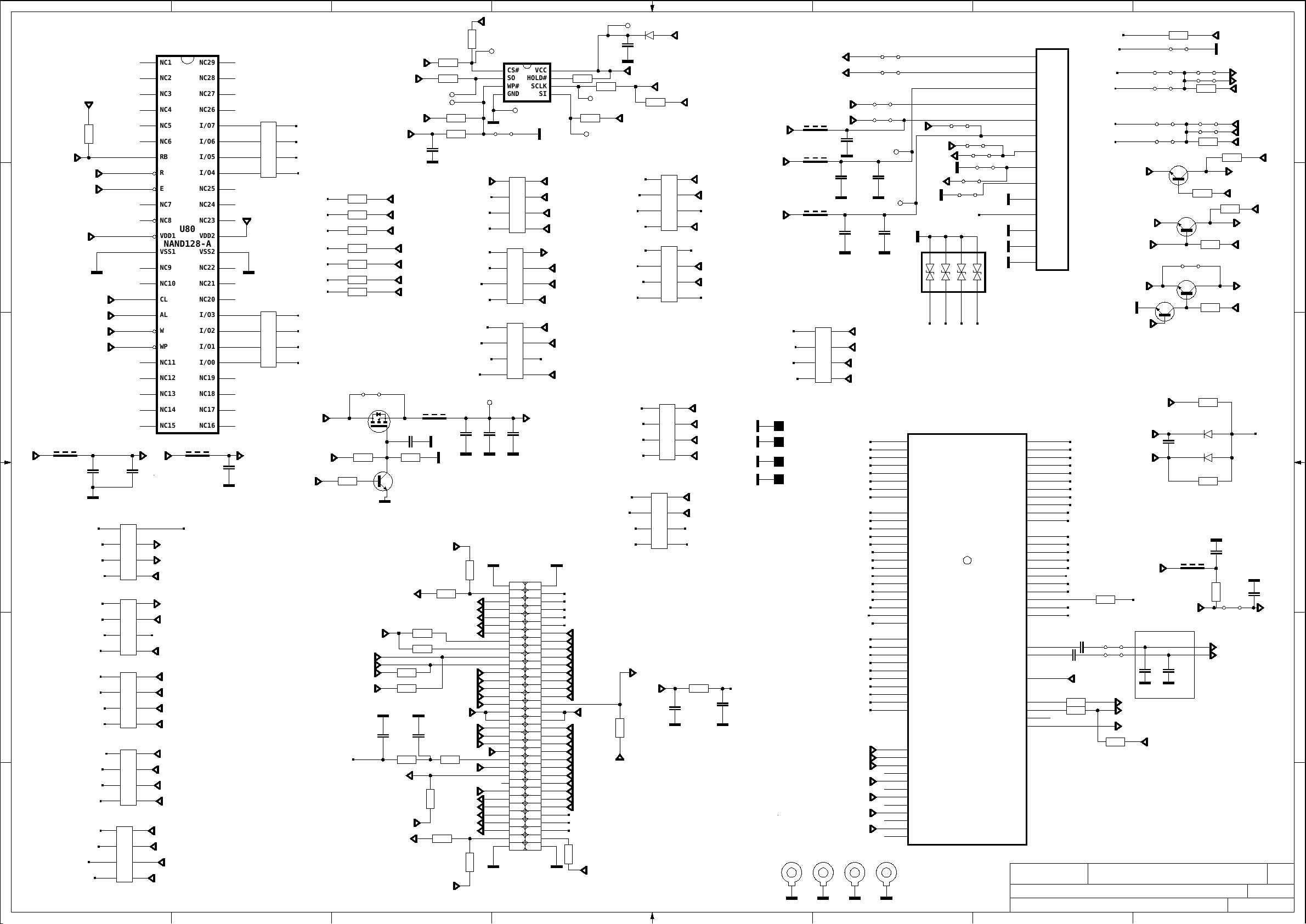
A
B
C
D
E
F
NAND_RBZ/CLK
NAND_REZ/IO4
NAND_CEZ/IO0
3V3_NAND2
NAND_CLE/IO2
NAND_WEZ/IO6
NAND_WPZ/IO1
F4
1k
PCM_IRQA_N
MCP_TS1_D[0]
PCM_WAIT_N
TS0_VALID
TS0_D_7
1 2 3 4 5 6 7 8
R2541
NAND_ALE
C1454
100n
16V
PCM_D[0]
PCM_REG_N
PCM_A_12
PCM_D[1]
PCM_A_4
TS0_D_6
TS0_D_4
PCM_A_1
TS0_D_2
TS0_D_0
TS0_D_3
TS0_D_1
TS0_D_5
TS0_SYNC
PCM_A_2
NAND FLASH
1
NC1
2
NC2
3
1
2
3
1
2
3
1
2
3
1
2
3
1
2
3
4
5
6
7
8
9
10
11
12
13
14
15
16
17
18
19
20
21
22
23
3V3_VCC
PCM-D[0]
PCM-D[1]
NC3
NC4
NC5
NC6
RB
R
E
NC7
NC8
U80
VDD1
NAND128-A
VSS1
NC9
NC10
CL
AL
W
WP
NC11
NC12
NC13
NC14
NC15 NC16
PCM_REG
PCM_IRQA
TS1_D0
PCM_WAIT
PCM_A12
PCM_A4
TS0_D6
TS0_D4
PCM_A1
TS0_D2
TS0_D0
TS0_D3
TS0_D1
TS0_D5
TS0-SYNC
TS0_VLD
TS0_D7
PCM_A2
3V3_NAND2
3k9
3V3_NAND3V3_VCC
C1453
100n
8
7
6
5 4
8
7
6
5 4
8
7
6
5 4
8
7
6
5 4
R2397
8
7
6
5 4
NAND_CEZ/IO0
16V
R2388
33R
R1
R2
R3
R4
R2391
33R
R1
R2
R3
R4
R2387
33R
R1
R2
R3
R4
R2389
33R
R1
R2
R3
R4
33R
R1
R2
R3
R4
F92
1k
NC29
NC28
NC27
NC26
I/O7
I/O6
I/O5
I/O4
NC25
NC24
NC23
VDD2
VSS2
NC22
NC21
NC20
I/O3
I/O2
I/O1
I/O0
NC19
NC18
NC17
C1352
100n
16V
48
47
46
45
44
43
42
41
40
39
38
37
36
35
34
33
32
31
30
29
28
27
26
2524
3V3_NAND2
R2402
75R
33R
8
1
R1
7
2
R2
6
3
R3
5 4
R4
NF_ALE/EMMC_IO8
NF_WPZ/EMMC_IO1
3V3_NAND
NF_CEZ/EMMC_IO0
NF_REZ/EMMC_IO4
NF_WEZ/EMMC_IO6
NF_CLE/EMMC_IO2
NF_RBZ/EMMC_IO10
R2401
75R
75R
33R
8
1
R1
7
2
R2
6
3
R3
5 4
R4
PCM_PWR_CTL
PCM_A_7
PCM_A_6
PCM_A_5
PCM_A_4
PCM_A_3
PCM_A_2
PCM_A_1
PCM_A_0
5V_VCC
12V_VCC
R8
33R
R10
33R
R11
33R
R7
33R
R6
33R
R9
33R
33R
R2812
S216
BSH103
Q58
R2457
1 2
47k
R2301
1 2
10k
3V3_VCC
PCM_IORD
PCM_IOWR
3V3_VCC
3V3_VCC
MCP_TS1_CLK
SPI-CS1N
SPI-SDO
3V3_STBY
FLASH-WPN1
NAND_ALE
NAND_WPZ/IO1
NAND_CEZ/IO0
NC
2
3
1
100n
1 2
Q57
BC847B
PCM_CD1
R2478
R2477
C1590
10p 50V
R2415
PCM_WAIT
CI_PWR
PCM_CD2
TP13
TP14
NAND_REZ/IO4
NAND_WEZ/IO6
NAND_CLE/IO2
NAND_RBZ/CLK
F1
60R
C1412
1
2
10V
47k
R2456
3V3_VCC
R2480
4k7
R2479
4k7
4k7
4k7
C1592
10p 50V
33R
4k7
R2481
R2692
3V3_VCC
R2405
33R
R2406
33R
R2483
4k7
R2407
33R
C1416
100n
10V
PCM_A_14
PCM_IORD_N
PCM_A_6
PCM_A_11
PCM_RST
PCM_A_13
PCM_A_8
PCM_OE_N
PCM_CE_N
PCM_A_9
PCM_D[5]
PCM_IOWR_N
C1351
10u
10V
R2408
33R
TS1_D3
TS1_D4
TS1_D5
TS1_D6
TS1_D7
TS0-SYNC
TS0_D0
TS0_D1
TS0_D2
TS0_D3
TS0_D4
TS0_D5
TS0_D6
R2720
33R
PCM-RST
PCM_REG
TS1_VLD
TS1_SYNC
TS1_D0
TS1_D1
TS1_D2
33R
3V3_STBY
4k7
R2482
TP16
U81
MX25L512
1
CS#
2
SO
3
WP#
4 5
TP1
NC
S206
VCC
HOLD#
SCLK
8
7
6
SIGND
MSTAR SPI FLASH
R2393
33R
8
1
2
3
1
2
3
1
2
3
CI_PWR
PCM_A14
PCM_IORD
PCM_A6
PCM_A11
PCM-RST
PCM_A13
PCM_A8
PCM_OE
PCM_CE
PCM_A9
PCM-D[5]
PCM_IOWR
C1414
100n
10V
TP3
1
2
1
7
6
5 4
R2394
33R
8
7
6
5 4
R2392
33R
8
7
6
5 4
C1413
100n
10V
R1
R2
R3
R4
R1
R2
R3
R4
R1
R2
R3
R4
2
1
CI
10k
R2300
TS0_D7
10k
R2299
CN26
35
36
37
38
39
40
41
42
43
44
45
46
47
48
49
50
51
52
53
54
55
56
57
58
59
60
61
62
63
64
65
66
67
68
1
2
3
4
5
6
7
8
9
10
11
12
13
14
15
16
17
18
19
20
21
22
23
24
25
26
27
28
29
30
31
32
33
34
PCM-D[3]
PCM-D[4]
PCM-D[5]
PCM-D[6]
PCM-D[7]
PCM-D[0]
PCM-D[1]
PCM-D[2]
4k7
R2476
4k7
TP15
R2404
33R
TP12
MCP_TS1_D[4]
MCP_TS1_D[7]
MCP_TS1_VALID
MCP_TS1_D[2]
MCP_TS1_D[3]
PCM_CE
PCM_A10
PCM_OE
PCM_A11
PCM_A9
PCM_A8
PCM_A13
PCM_A14
PCM_WE
CI_PWRCI_PWR
TS0_VLD
TS0_CLK
PCM_A12
PCM_A7
PCM_A6
PCM_A5
PCM_A4
PCM_A3
PCM_A2
PCM_A1
PCM_A0
R2484
CI_PWR
TP2
C1415
1N5819
100n
10V
3V3_SPI
R2403
33R
SPI-SDI
PCM_D[7]
PCM_A_10
PCM_D[3]
MCP_TS1_D[1]
PCM_D[6]
PCM_WE_N
PCM_A_0
PCM_A_5
PCM_A_3
PCM_D[4]
PCM_D[2]
PCM_IRQA
TS0_CLK
4k7
R2490
CI_PWR
D58
R2486
4k7
R2390
8
7
6
SPI-SCK
R2399
33R
8
R1
7
R2
6
R3
R4
R2398
33R
8
R1
7
R2
6
R3
5 4
R4
R2396
33R
8
R1
7
R2
6
R3
5 4
R4
33R
1
R1
2
R2
3
R3
45
R4
3V3_STBY
3V3_STBY
1
2
3
45
1
2
3
1
2
3
PCM-D[4]
PCM-D[2]
R2421
C1593
50V 10p
ET_TP
ET_TN
Ethernet lines must be 100ohm differential pairs
ET_RP
ET_RN
F91
1k
F3
1k
F78
1k
R2395
33R
8
R1
7
R2
6
R3
5 4
R4
GS5
GS6
GS7
GS8
NF_CEZ/EMMC_IO0
NF_WPZ/EMMC_IO1
NF_CLE/EMMC_IO2
NF_REZ/EMMC_IO4
NF_WEZ/EMMC_IO6
NF_ALE/EMMC_IO8
NF_RBZ/EMMC_IO10
PL1
C1941
1u
6V3
C1565
1u
6V3
C1819
1u
6V3
1
TS1_D6
2
PCM_A7
3
TS1_D5
TS1_SYNC
PCM_D[0]
PCM_D[1]
PCM_D[2]
PCM_D[3]
PCM_D[4]
PCM_D[5]
PCM_D[6]
PCM_D[7]
PCM_A_0
PCM_A_1
PCM_A_2
PCM_A_3
PCM_A_4
PCM_A_5
PCM_A_6
PCM_A_7
PCM_A_8
PCM_A_9
PCM_A_10
PCM_A_11
PCM_A_12
PCM_A_13
PCM_A_14
PCM_RST
PCM_IRQA_N
PCM_IOWR_N
PCM_OE_N
PCM_WAIT_N
PCM_IORD_N
PCM_CD_N
PCM_REG_N
PCM_WE_N
PCM_CE_N
PL2
PL3
TS1_D4
TS1_D7
PCM-D[7]
PCM_A10
PCM-D[3]
TS1_VLD
TS1_D1
PCM-D[6]
PCM_WE
TS1_D2
PCM_A0
TS1_D3
PCM_A5
PCM_A3
33R
TS0_CLK_MST
10p
C1591
50V
5V_STBY
5V_STBY
5V_STBY
MCP_TS1_D[6]
PCM_A_7
MCP_TS1_D[5]
MCP_TS1_SYNC
S204
S205
S210
S211
TP4
C1666
100n
16V
TP175
IR_to_RJ48
IR_to_RJ48
IR_CONTROL
IR_from_RJ48
C21
100n
16V
AB19
AB23
AB20
AB21
AA21
AC22
AA23
AA22
AB22
AA15
AC16
AB16
AC15
AB15
AA14
AB17
AA16
AB14
AB18
AC18
AA17
W16
W15
V20
W20
W19
Y13
Y20
U18
V15
U19
V22
W18
Y22
V23
W14
Y21
W22
V16
W21
Y14
W23
U20
Y16
V18
8
1
PCM_D0
PCM_D1
PCM_D2
PCM_D3
PCM_D4
PCM_D5
PCM_D6
PCM_D7
PCM_A0
PCM_A1
PCM_A2
PCM_A3
PCM_A4
PCM_A5
PCM_A6
PCM_A7
PCM_A8
PCM_A9
PCM_A10
PCM_A11
PCM_A12
PCM_A13
PCM_A14
PCM_RESET
PCM_IRQA_N
PCM_IOWR_N
PCM_OE_N
PCM_WAIT_N
PCM_IORD_N
PCM_CD_N
PCM_REG_N
PCM_WE_N
PCM_CE_N
EMMC_IO[0]/NAND_CEZ
EMMC_IO[1]/NAND_WPZ
EMMC_IO[2]/NAND_CLE
EMMC_IO[3]
EMMC_IO[4]/NAND_REZ
EMMC_IO[5]/NAND_CEZ1
EMMC_IO[6]/NAND_WEZ
EMMC_IO[7]
EMMC_IO[8]/NAND_ALE
EMMC_IO[9]
EMMC_IO[10]/NAND_RBZ
EMMC_IO[11]
PL4
ETHERNET
1
2
3
4
5
6
7
8
9
10
11
ETH_pin11
12
13
14
TS0_D0
AA19
TS0_D1
TS0_D2
TS0_D3
AA20
TS0_D4
AA18
TS0_D5
INPUT
TS0_D6
AC21
TS0_D7
TS0_CLK
TS0_VLD
TS1_CLK
TS1_VLD
TS1_D0
TS1_D1
TS1_D2
TS1_D3
TS1_D4
TS1_D5
TS1_D6
IN / OUT
TS1_D7
VIFP
VIFM
IFAGC
TGPIO0
TGPIO1
AC19
VESTEL
SCH NAME :
DRAWN BY :
S431
S458
7
CDA4C16GTH
2
ETH_pin1
ETH_pin2
U95
MSD-G7
ETH_pin1
ETH_pin2
ETH_pin3
ETH_pin4
S459
S452
S425
S453
6
54
D65
3
ETH_pin4
ETH_pin3
TS0_SYNC
2
TS1_SYNC
TGPIO2/I2C_CLK
TGPIO3/I2C_SDA
CN10
TD+
TD-
TCT
RD+
RD-
RCT
NC1
NC2
GR+
GR-
YL+
YL-
SHLD1
SHLD2
W17
Y19
V19
V17
V14
Y18
V10
Y11
V13
W11
W13
W12
V11
W10
V12
Y9
W9
AB1
AB2
AC2
AA2
AA1
AA4
AB4
MCP_TS1_D[0]
MCP_TS1_D[1]
MCP_TS1_D[2]
MCP_TS1_D[3]
MCP_TS1_D[4]
MCP_TS1_D[5]
MCP_TS1_D[6]
MCP_TS1_D[7]
MCP_TS1_CLK
MCP_TS1_VALID
MCP_TS1_SYNC
TS0_D_0
TS0_D_1
TS0_D_2
TS0_D_3
TS0_D_4
TS0_D_5
TS0_D_6
TS0_D_7
TS0_VALID
TS0_SYNC
C1851
100n
16V
R2897
33R
R2814
33R
100n
C1850
IF-AGC
CI_NAND_SPI_ETH
<YOUR NAME HERE>
ETH_pin11
ETH_pin1
3V3_VCC
PCM_CD1
PCM_CD2
3V3_VCC
TS0_CLK_MST
C1902
100p
50V
close to MST
HP_DETECT
S2_RESET
HUB_RESET
3V3_VCC
S448
S449
S451
S450
BC848B
ETH_pin1
ETH_pin2
ETH_pin3
ETH_pin2
IR_from_RJ48 IR_IN
IR_CONTROL
IR_CONTROL
33R
R2813
S422
16V
S421
R2871
1 2
10k
PROJECT NAME :
R2900
10k
Q18 BC848B
Q68
S454
BC848B
Q70
C1871
1n
50V
IF-AGC
C1901
100p
50V
12
S447
S427
S428
10k
R2693
S429
S430
10k
R2694
R2876
1 2
10k
R2901
1 2
10k
BC848BQ69
R2902
1 2
10k
R2873
1 2
10k
1N4148
D93
1N4148
D94
R2874
1 2
10k
F88
1k
3V3_VCC
12
12
1 2
R2903
1 2
C1828
100n
16V
10k
R2872
MST_IF_P
MST_IF_N
17mb110-r2
87654321
UART-RX
RX_HOTEL
3V3_STBY
UART-TX
TX_HOTEL
3V3_STBY
R1
10k
IR_to_RJ48IR_RC
3V3_STBY
10k
S423
3V3_STBY
3V3_STBY
IR_INIR_RC
3V3_STBY
PCM_CD_N
C1908
16V
22n
3V3_STBY
IF_AGC
A3
T. SHT:
9
13-10-2015_19:40
A
B
C
D
E
F
AX M
Page 62
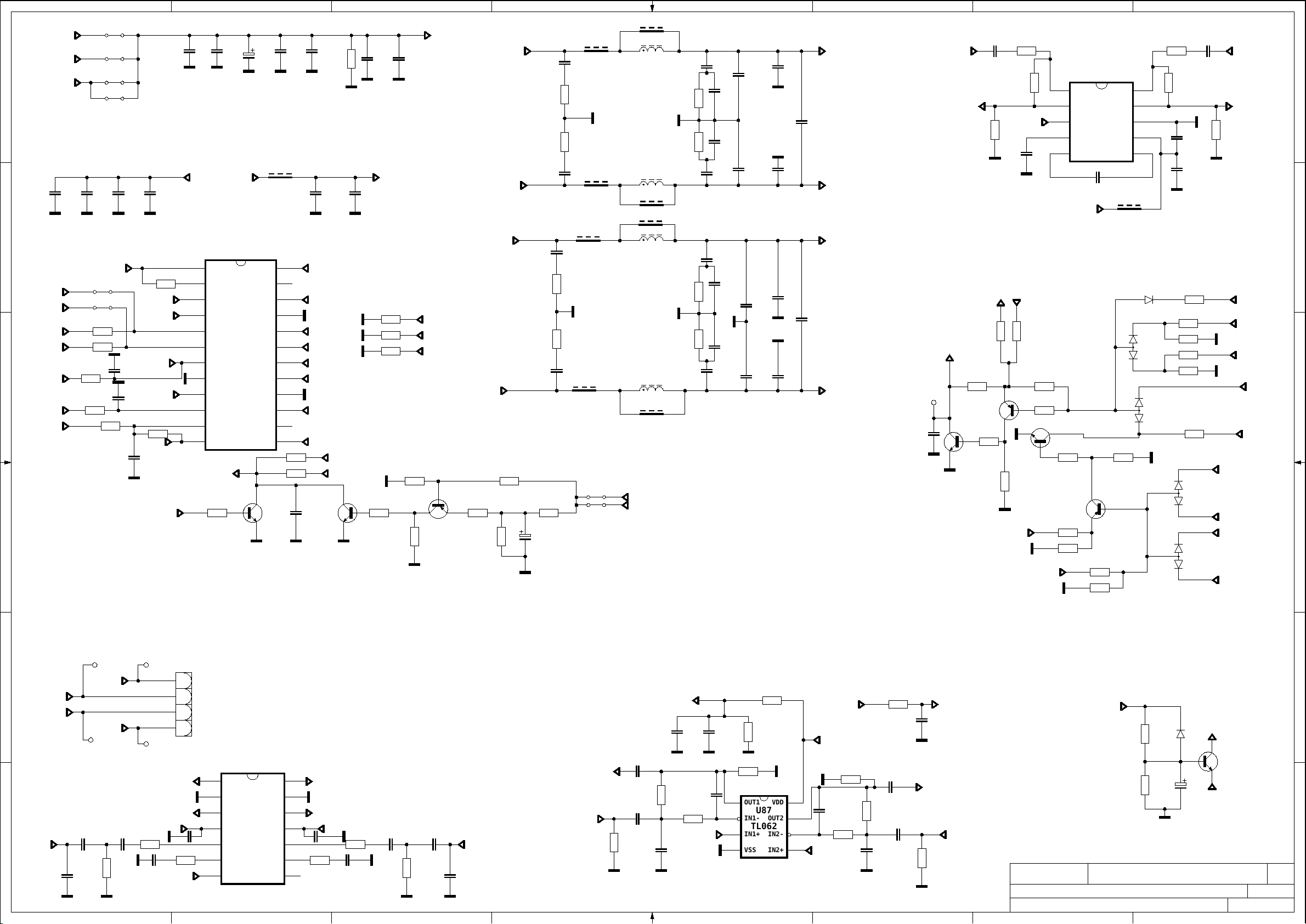
1 2 3 4 5 6 7 8
12
12
F6
60R
L4
10u
15u
L5
15u
10u
F7
60R
F8
60R
L2
10u
15u
L3
10u
15u
F9
60R
VDD_AUDIO
12V_VCC
C1334
18R
R2215
18R
R2216
C1335
C1337
18R
R2217
18R
R2218
C1336
50V
100n
C1338
220n
50V
C1339
220n
50V
50V
100n
50V
100n
C1341
220n
50V
C1340
220n
50V
50V
100n
C312
220n
50V
C313
220n
50V
C311
220n
50V
C307
220n
50V
C286
1u
50V
30068742
C287
1u
50V
C288
1u
50V
30068742
C302
1u
50V
C698
220n
50V
C699
220n
50V
L_OUT_P
L_OUT_N
R_OUT_P
R_OUT_N
C34
100n
10V
C1658
R2304
12
HP_RIGHT
HP_OUT_R HP_OUT_L
1u
6V3
4k7
R2495
10k
R2237
AMP_EN
12
33k
1
2
3
4
C1656
5 6
1u
6V3
3V3_VCC
HEADPHONE AMP
-INR
OUTR
EN
PVSS
U85
AD22657B
C1566
1u
16V
-INL
OUTL
GND
PVDD
CPCN
F46
1k
1 2
10
9
8
7
R2303
10k
12
33k
R2238
C1657
1u
6V3
C1353
10u
10V
C1659
1u
6V3
4k7
R2496
SHORT CCT PROTECTION
2
1
Q19
TP23
1
PROTECT
3
2
1
BC848B
R2305
10k
BC858B
1 2
Q51
R83
10k
R2776
12
R82
3V3_VCC
3V3_VCC
3V3_STBY
12
10k1210k
R2777
10k
1 2
R85
10k
R84
1 2
10k
BC848B
Q20
3V3_VCC
12
R322
100R
BC858B
R804
6k8
10k
R88
Q50
12
R2771
6k8
10k
R2770
12
R657
47k
3
1 2
D95
1N4148
D40
3
1 2
BAW56
D39
BAW56
1 2
R490
33k
R81
5k1
R494
10k
R86
3k9
1 2
3
1 2
3
1 2
R2877
10k
R92
10k
D86
D87
12
VDDC
BAW56
1V5_VCC
1V15_POK
BAW56
1V3_SAT_VCC
HP_LEFT
3V3_WOWL
24V_VCC_AU
12V_VCC
5V_VCC
3V3_VCC
A
B
C
D
C1331
R2223
4k7
R2214
4k73V3_AMP
100n
50V
AMP_EN
S444
S445
R2211
100R
R2212
100R
R2210
100R
S116
S200
S93
S141
C1332
C1350
100n
50V
16V
100n
C1328
100n
16V
C1329
12p
50V
100n
C1333
AOSDATA0
AOLRCK
AMP_RESET
3V3_AMP
R2209
100R
AOBCK
AMP_MUTE
50V
R2213
100R
C1792
10u 10u
10V
VDD_AUDIO
1
PD
2
ERROR
3
SDATA
4
LRCIN
5
SDA
6
SCL
7
RESET
8
DGND
9
DVDD
10
SA0
11
MCLK
12
BCLK
AMP_EN
R78
1 2
10k
C1791
10V
3V3_VCC
8W 30067972
VDDLA
N.C.2
U62
VDDLB
AD82587D
VDDRB
N.C.1
VDDRA
3
2
1
C1742
220u
10V
GNDL
GNDR
F5
60R
LA
LB
RB
RA
BC848B
Q8
C674
10u
10V
24
23
22
21
20
19
18
17
16
15
14
13
R2714
4k7
4k7
R824
C675
10u
10V
C245
100n
16V
3V3_AMP
R647
10k
C704
10u
16V
C1195
10u
16V
3V3_AMP
C1196
10u
16V
NC
I2C: 0x60 LOW, 0x68 HIGH
VDD_AUDIO
A_OUT1A
R2120
A_OUT1B
VDD_AUDIO
VDD_AUDIO
A_OUT2B
A_OUT2A
VDD_AUDIO
NC
C146
100n
16V
5V_VCC
3V3_VCC
3
Q7
1
BC848B
2
1 2
R2121
1 2
R2122
1 2
R489
33k
10k
10k
10k
R692
1 2
100k
100k
R691
1 2
AOBCK
AOLRCK
AOMCLK
VDD_AUDIO
Q49
BC858B
A_OUT2B
10k
1 2
R79
A_OUT1A
A_OUT1B
A_OUT2A
1 2
10k
R1983
10k
R80
1 2
C620
470p
470p
470p
50V
470p
50V
1 2
12
100u
16V
C5
C3
50V
50V
10k
R93
F63
C1
60R
R2
R3
10R 10R
C2
F64
60R
F65
60R
R5R4
10R
10R
F66
60R
S22
S21
12V_VCC
24V_VCC_AU
A
5V_VCC
100n
C1330
50V
B
3V3_STBY
3V3_STBY
SYS_SDA
SYS_SCL
3V3_AMP
C
AOMCLK
D
TP20TP17
CN19
E
R_OUT_N
R_OUT_P
L_OUT_P
L_OUT_N
TP21
F
C250
1u
C140
100n C141
10V
NC
RIGHT
6V3
C193
220n 10V
R2712
R2718 R2717
150k
6V3 1u
10k
1
2
3
4
TP19
2w5 30069845
C1790
A_OUT1A
A_OUT1B
C1788
R2716
150k
AMP_EN
1
OUTPL
2
VSSL
3
OUTNL
VDDL
AD52010
INL+
INL-
SDN
U91
4
1u
6V3
5
6
7
OUTPR
VSSR
OUTNR
VDDR
INR+
INR-
14
A_OUT2A
13
12
A_OUT2B
11
10
9
8
NC
1u
6V3
R2715
150k
C1787
VDD_AUDIOVDD_AUDIO
150k
1u
6V3
C1789
C191
220n 10V
AUDIO AMP for 16" to 24"
10k
C251
1u
R2713
6V3
E
33k
1 2
R2242
33k
1
OUT1
2
IN1-
TL062
3
IN1+
VSS IN2+
33k
1 2
R2240
R2239
12
VDD
U87
OUT2
IN2-
12V_VCC 47R
VDD_Lineout
8
7
6
54
C1710
12p
50V
R2627
VDD_AUDIO/2
R2241
1 2
33k
68k
56k
C1738
150p
50V
C1355
10u
10V
R2665
R2667
C1660
1u
6V3
VDD_Lineout
C1722
10u
16V
SC_AUD_L_OUT
100k
R2225
SC_DAC_L
VESTEL
SCH NAME :
DRAWN BY :
AUDIO
<YOUR NAME HERE>
12V_VCC
120k
47k
R2778 R2779
PROJECT NAME :
STBY_ON/OFF
D88
1N4148
BC848B
Q62
C1824
47u
16V
PROTECT
17mb110-r2
87654321
A3
T. SHT:
9
13-10-2015_18:11
F
AX M
VDD_AUDIO/2
C1721
C1419
10u
100n
16V
10V
100k
R2224
C1354
10u
10V
C1661
1u
6V3
56k
R2666
R2626
VDD_AUDIO/2
C1739
150p
50V
C1709
68k
12p
50V
SC_AUD_R_OUT
SC_DAC_R
MAIN_RMAIN_L
100n
NC
10V
Page 63
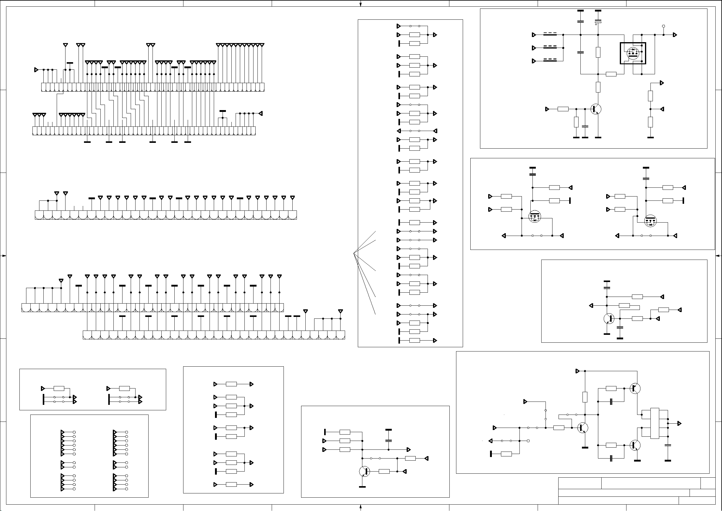
1 2 3 4 5 6 7 8
A
B
C
D
FHD 50Hz 3D FFC
OP_PIN42
OP_PIN43
OP_PIN46
TX_2_CLK_P
TX_2_CLK_N
TX_2_2_P
TX_2_4_N
TX_2_4_P
TX_2_3_P
TX_2_3_N
TX_2_2_N
PANEL_VCC
32
33
34
35
36
37
38
39
40
41
42
43
44
45
46
47
48
49
50
51
OP_PIN42
OP_PIN45
OP_PIN44
OP_PIN41
OP_PIN40
OP_PIN51
PAN_SCL
PAN_SDA
49
50
51
48
OP_PIN43
30
31
32
33
34
35
36
37
38
39
40
41
42
43
44
45
46
47
19" TO 22" DOUBLE LVDS FFC OPTIONS
PANEL_VCC
CN14
OP_PIN9
1
2
3
4
5
TX_2_3_P
TX_2_3_N
TX_2_CLK_N
TX_2_CLK_P
6
7
8
9
10
11
WXGA FFC
OP_PIN9
OP_PIN8
OP_PIN27
SAM
1
CN15
OP_PIN11
PANEL_VCC
2
3
4
5
6
LG
7
CN16
8
1
OP_PIN7
9
10
2
3
11
12
4
5
TX_2_1_N
TX_2_1_P
TX_2_0_P
29
30
31
27
28
29
TX_2_2_P
12
TX_1_3_N
TX_1_3_P
13
14
6
7
OP_PIN27
OP_PIN26
TX_2_0_N
26
27
28
24
25
26
TX_2_2_N
13
14
15
8
TX_1_4_N
TX_1_4_P
24
25
22
23
TX_2_1_P
15
TX_1_CLK_P
16
9
TX_1_CLK_P
TX_1_3_N
TX_1_3_P
20
21
22
23
18
19
20
21
TX_2_1_N
16
17
TX_1_CLK_N
17
18
10
11
TX_1_2_N
TX_1_2_P
TX_1_CLK_N
16
17
18
19
14
15
16
17
TX_2_0_N
TX_2_0_P
18
19
TX_1_2_N
TX_1_2_P
19
20
12
13
TX_1_0_P
TX_1_1_N
TX_1_1_P
13
14
15
11
12
13
TX_1_3_P
20
TX_1_1_P
21
22
14
15
OP_PIN10
OP_PIN11
TX_1_0_N
10
11
12
10
TX_1_3_N
TX_1_CLK_P
21
22
TX_1_1_N
23
16
OP_PIN9
OP_PIN8
OP_PIN7
TX_1_CLK_N
23
TX_1_0_P
24
25
17
18
OP_PIN4
OP_PIN6
OP_PIN5
TX_1_2_P
24
25
TX_1_0_N
26
19
OP_PIN1
PAN_SCL
PAN_SDA
123456789
LG BASED 30070519
CN18
PANEL_VCC
123456789
SAM BASED 30070519
CN17
TX_1_2_N
TX_1_1_P
TX_1_1_N
TX_1_0_P
TX_1_0_N
26
27
28
29
30
OP_PIN5
OP_PIN10
OP_PIN6
27
28
29
30
20
21
22
23
OP_PIN26
24
25
26
27
28
15.6"
PANEL_VCC
29
30
OPTIONS TABLE
3D_SYNC_OUT
PANEL_VCC OP_PIN5
3V3_VCC 10k
PANEL_VCC
PANEL_VCC
MEGA_DCR_IN
PANEL_VCC
MEGA_DCR_OUT
PANEL_VCC
PANEL_VCC
PANEL_VCC
PANEL_VCC
12V_VCC
12V_VCC
3D_EN
PANEL_VCC
12V_VCC
PANEL_VCC OP_PIN43
BACKLIGHT_ON/OFF
DIMMING
PANEL_VCC
S243
R2246
33k
R2317
1 2
10k
R2328
1 2
R2248
33k
R2318
1 2
10k
R2249
33k
R2320
1 2
10k
S244
1 2
R2250
33k
R2321
1 2
10k
S233
R2251
33k
R2322
1 2
10k
R2245
33k
R2319
1 2
10k
R2243
33k
R2315
1 2
10k
R2247
33k
R2316
1 2
10k
R2313
1 2
10k
S235
1 2
S236
1 2
S245
R2252
33k
R2323
1 2
10k
S237
1 2
R2253
33k
R2324
1 2
10k
S238
1 2
S234
1 2
R2244
33k
R2314
1 2
10k
R2312
1 2
10k
12
12
12
OP_PIN6
OP_PIN7
OP_PIN8
OP_PIN9
OP_PIN9
OP_PIN10
OP_PIN11
OP_PIN27
OP_PIN26
OP_PIN40
OP_PIN41
OP_PIN42
OP_PIN44
OP_PIN45
OP_PIN46
12V_VCC
5V_VCC
5V_VCC
F16
60R
F18
60R
F19
60R
PANEL SUPPLY SWITCH
PANEL_VCC_ON/OFF
C1541
100n
16V
1 2
R2264
PAN_SCL
1 2
33k
R2259
1 2
33k
Q29
S251
BSN20
1 2
5V_VCC
3V3_VCC
C1736
100u
16V
16V
100n
C1539
21
25V
33k
220n
R2326
10k
12
C1389
12
10k
R2327
R2255
C1741
1n
50V
1 2
12
33k
Q31
BC848B
R2256
R2278
1 2
47R
PANEL I2C BUFFER
R2260
33k
R2258
33k
PANEL_VCC
5V_VCC
3V3_VCC
PAN_SDA
Backlight On/Off Circuit
C1422
BACKLIGHT_ON/OFF
Q27
BC848B
R2265
1 2
33k
R2261
1 2
33k
10V
100n
nc
R2504
4k7
1 2
C1423
3 4
R2502
4k7
1 2
R2503
4k7
1 2
10V
100n
TP65
PANEL_VCC
5
6
A
Q43
FDC642P
1
2
PANEL_VCC
12
33k
R2254
BACKLIGHT_ON/OFF
12
10k
R2325
B
C1542
100n
16V
R2262
1 2
33k
R2263
1 2
33k
PANEL_VCC
C
S252
Q30
BSN20
R2501
1 2
MST_BACKLIGHT_ON/OFF
4k7
5V_VCC
SYS_SDASYS_SCL
D
3V3_STBY
Dimming
Options Table
E
3V3_VCC
10_BIT PANEL
R2740
1 2
10k
S242
1 2
S241
1 2
TX_1_4_N
TX_1_4_P
3V3_VCC
1
1
R2739
1 2
10k
S239
S240
2
2
TX_2_4_N
TX_2_4_P
3D_EN
3V3_VCC
PANEL_VCC
Test Pins
TX_1_0_N
TX_1_0_P
TX_1_1_N
TX_1_1_P
TX_1_2_N
TX_1_2_P
F
TX_1_CLK_N
TX_1_CLK_P
TX_1_3_N
TX_1_3_P
TX_1_4_N
TX_1_4_P
TP53
TP54
TP55
TP56
TP57
TP58
TP64
TP59
TP60
TP61
TP62
TP63
TX_2_0_N
TX_2_0_P
TX_2_1_N
TX_2_1_P
TX_2_2_N
TX_2_2_P
TX_2_CLK_N
TX_2_CLK_P
TX_2_3_N
TX_2_3_P
TX_2_4_N
TX_2_4_P
TP41
TP42
TP43
TP44
TP45
TP46
TP47
TP48
TP49
TP50
TP51
TP52
3V3_VCC 10k
PANEL_VCC
3V3_VCC
R2329
1 2
10k
R2330
1 2
10k
R2257
33k
R2331
1 2
10k
R2335
1 2
10k
R2336
1 2
10k
R2333
1 2
R2266
33k
R2332
1 2
10k
R2334
1 2
10k
OP_PIN26
OP_PIN4
OP_PIN13D_EN
OP_PIN51
OP_PIN27
3D ENABLE
R2507
12
4k7
R2509
5V_VCC
3V3_VCC 3D_EN
4k7
R2506
4k7
BC848B
12
12
Q28
S250
3
2
1
nc
4k7
1 2
R2505
C1540
100n
16V
4k7
1 2
R2508
3D_ENABLE
3V3_VCC
BACKLIGHT_DIM
MEGA_DCR_IN
MEGA_DCR_OUT
S247
R2685
1 2
10k
NC
S248
TP40
3V3_VCC
S249
R2499
1 2
4k7
VESTEL
SCH NAME :
DRAWN BY :
1k
R2286
1 2
S246
Q25
BC848B
LVDS
<YOUR NAME HERE>
R2498
1 2
4k7
C1675
21
220p
50V
R2500
1 2
4k7
C1676
21
50V220p
PROJECT NAME :
BC858B
Q54
R4
45
R3
3
6
R2
2
7
R1
1
8
100R
Q26
R2660
BC848B
17mb110-r2
87654321
DIMMING
C1723
10u
16V
T. SHT:
13-10-2015_18:11
E
F
A3
9
AX M
 Loading...