

MB100 IDTV
SERVICE MANUAL

Table of Contents
1. INTRODUCTION .......................................................................................................................................................... 2
2. TUNER ........................................................................................................................................................................... 2
A. SI2157 TerrestrIal and Cable TV Tuner ...................................................................................................................... 2
B. M88TS2022 Satellıte Tuner ........................................................................................................................................ 5
3. AUDIO AMPLIFIER STAGES ...................................................................................................................................... 6
A. MAIN AMPLIFIER (TAS5719) ...................................................................................................................................... 6
B. HEAD-PHONE AMPLIFIER STAGE .............................................................................................................................. 10
C. SUBWOOFER AMPLIFIER STAGE .............................................................................................................................. 11
4. POWER STAGE ........................................................................................................................................................... 16
5. MICROCONTROLLER (MSTAR MSD95C0H) ......................................................................................................... 30
6. VIDEO BACK-END PROCESSOR (MSTAR) ........................................................................................................... 37
7. 1Gb DDR3 SDRAM ..................................................................................................................................................... 41
8. 2Gb DDR3 SDRAM ..................................................................................................................................................... 42
9. 32Gbit (4G x 8 bit) NAND Flash Memory ................................................................................................................... 43
10. 16M-BIT [16M x 1] CMOS SERIAL FLASH EEPROM ............................................................................................ 45
11. Demodulator Stage ........................................................................................................................................................ 49
12. LNB supply and control IC ........................................................................................................................................... 53
13. Troubleshootıng ............................................................................................................................................................ 54
A. No Backlıght Problem .............................................................................................................................................. 54
D. CI Module Problem .................................................................................................................................................. 56
E. Stayıng ın Stand-by Mode ........................................................................................................................................ 58
F. IR Problem ................................................................................................................................................................ 58
G. Keypad Touchpad Problems ...................................................................................................
H. USB Problems ........................................................................................................................................................... 59
İ. No Sound Problem ................................................................................................................................................... 60
J. Standby On/Off Problem ......................................................................................................................................... 61
K. No Sıgnal Problem .................................................................................................................................................... 61
14. General Block Dıagram ................................................................................................................................................ 63
................................. 59
15. PLACEMENT OF BLOCKS ........................................................................................................................................ 64
1

1. INTRODUCTION
17MB100 main board is driven by MStar SOC. This IC is a single chip iDTV solution that supports channel
decoding, MPEG decoding, and media-center functionality enabled by a high performance AV CODEC and
CPU. This IC also supports 4K2K (UHD).
Key features includes,
Combo Front-End Demodulator
A multi standart A/V format decoder
The MACEpro video processor
Home theatre sound processor
Internet and Variety of Connectivity Support
Dual-stream decoder for 3D contents
Mılti-purpose CPU for OS and multimedia
Peripheral and power management
Supported peripherals are:
1 RF input VHF I, VHF III, UHF
1 Satellite input
1 Side AV (CVBS, R/L_Audio)
1 Side SCART socket(Common)
1 YPbPr (Common)
1 Side S-Video(Common)
1 PC input(Common)
4 HDMI input(Common)
1 Common interface(Common)
1 Optic S/PDIF output(Common)
1 Stereo audio input for PC(Common)
1 Subwoofer output(Common)
1 Headphone(Common)
2x USB3.0 and 1xUSB2.0(Common)
1 Ethernet-RJ45 (Common)
1 External Touchpad(Common)
Internal Wi-Fi and BT
2. TUNER
A. SI2157 TERRESTRIAL AND CABLE TV TUNER
Description
The Si2157 is Silicon Labs' fifth-generation hybrid TV tuner supporting all worldwide terrestrial and cable TV
standards. Requiring no external balun, SAW filters, wirewound inductors or LNAs, the Si2157 offers the
lowest-cost BOM for a hybrid TV tuner. Also included are an integrated power-on reset circuit and an option
for single power supply operation. As with prior-generation Silicon Labs TV tuners, the Si2157 maintains very
high linearity and low noise to deliver superior picture quality and a higher number of received stations when
compared to other silicon tuners and discrete MOPLL-based tuners. The Si2157 also incorporates a harmonicrejection mixer to deliver excellent Wi-Fi and LTE immunity. For the best performance with next-generation
digital TV standards such as DVB-T2/C2, the Si2157 delivers industry-leading phase noise performance.
2
Features
Worldwide hybrid TV tuner
o Analog TV: NTSC, PAL/SECAM
o Digital TV: ATSC/QAM, DVBT2/T/C2/C, ISDB-T/C, DTMB
o 42-1002 MHz frequency range
Industry-leading margin to A/74,
NorDig, DTG, ARIB, EN55020,
OpenCable™
Lowest BOM for a hybrid TV tuner
o No balun at RF input
o Integrated tracking filters requiring no external inductors or SAW filters
o Increased ESD protection on 6 pins
Best-in-class real-world reception
o Exceeds MOPLL-based tuners
o Lowest phase noise
o High Wi-Fi and LTE immunity
Low power consumption
o 3.3 V and 1.8 V power supplies
o 3.3 V single-supply option
Integrated power-on reset circuit
Single or separate output pins for ALIF/DLIF connection to SoC
Standard CMOS process
4 x 4 mm, 28-pin QFN package
RoHS compliant
3
Figure: Si2157 Pin description
4
Table: Pin Functions
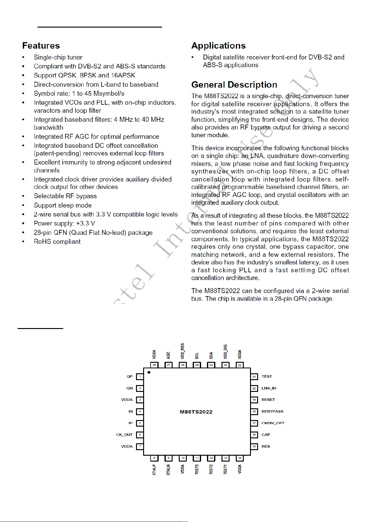
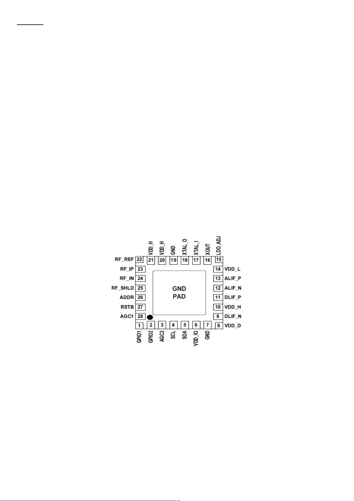
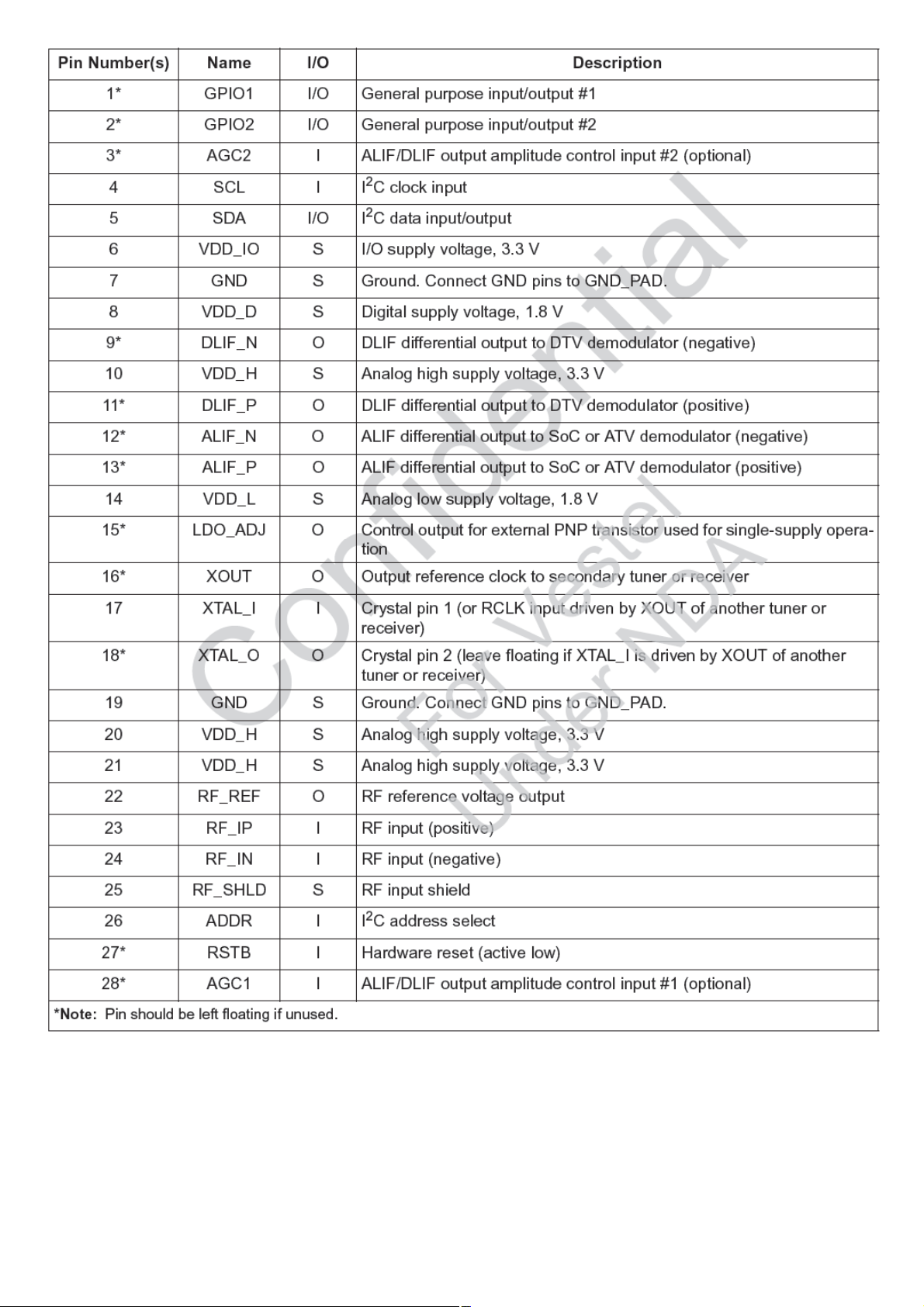
B. M88TS2022 SATELLITE TUNER
Pin Assigment
5
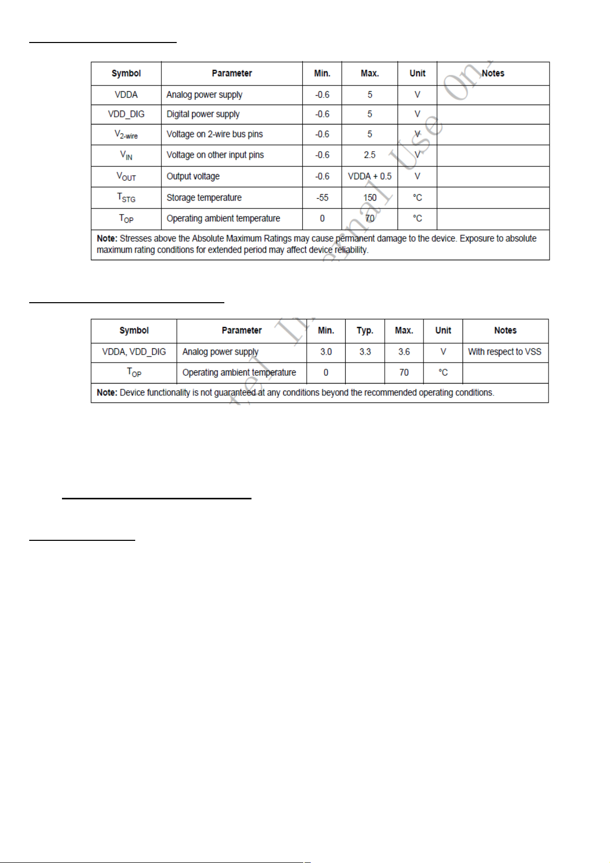
Absolute Maximum Ratings
Recommended Operating Conditions
3. AUDIO AMPLIFIER STAGES
A. MAIN AMPLIFIER (TAS5719)
General Description
The TAS5717/TAS5719 is a 10-W/15-W, efficient,digital audio-power amplifier for driving stereo bridgetied speakers. One serial data input allows processing of up to two discrete audio channels and seamless
integration to most digital audio processors and MPEG decoders. The device accepts a wide of input data and
data rates. A fully programmable data path routes these channels to the internal speaker drivers.
The TAS5717/9 is a slave-only device receiving all clocks from external sources. The TAS5717/TAS5719
operates with a PWM carrier between a 384-kHz switching rate and a 352-KHz switching rate, depending on
the input sample rate. Oversampling combined with a fourth-order noise shaper provides a flat noise floor and
excellent dynamic range from 20 Hz to 20 kHz.
6

Features
• Audio Input/Output
o TAS5717 Supports 2×10 W and TAS5719 Supports 2×15 W Output
o Wide PVDD Range, From 4.5 V to 26 V
o Efficient Class-D Operation Eliminates Need for Heatsinks
o Requires Only 3.3 V and PVDD
o One Serial Audio Input (Two Audio Channels)
o I2C Address Selection via PIN (Chip Select)
o Supports 8-kHz to 48-kHz Sample Rate (LJ/RJ/I2S)
o External Headphone-Amplifier Shutdown Signal
o Integrated CAP-Free Headphone Amplifier
o Stereo Headphone (Stereo 2-V RMS Line Driver) Outputs
• Audio/PWM Processing
o Independent Channel Volume Controls With 24-dB to Mute
o Programmable Two-Band Dynamic Range Control
o 14 Programmable Biquads for Speaker EQ
o Programmable Coefficients for DRC Filters
o DC Blocking Filters
o 0.125-dB Fine Volume Support
• General Features
o Serial Control Interface Operational Without MCLK
o Factory-Trimmed Internal Oscillator for Automatic Rate Detection
o Surface Mount, 48-Pin, 7-mm × 7-mm HTQFP Package
o AD, BD, and Ternary PWM-Mode Support
o Thermal and Short-Circuit Protection
• Benefits
o EQ: Speaker Equalization Improves Audio Performance
o DRC: Dynamic Range Compression. Can Be Used As Power Limiter. Enables Speaker Protection,
Easy Listening, Night-Mode Listening
o DirectPath Technology: Eliminates Bulky DC Blocking Capacitors
o Stereo Headphone/Stereo Line Drivers: Adjust Gain via External Resistors, Dedicated Active
Headpone Mute Pin, High Signal-to-Noise Ratio
o Two-Band DRC: Set Two Different Thresholds for Low- and High-Frequency Content
7
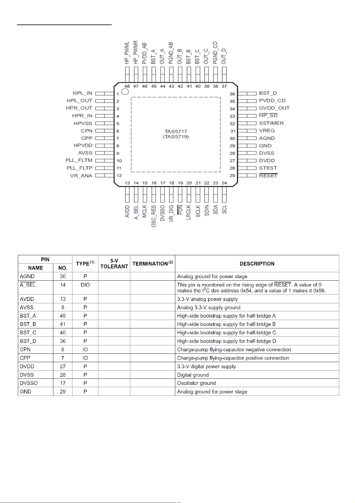
Pin descriptions and functions:
Figure: TAS5719 Pin descriptions
8
Table: TAS5719 Pin Functions
9
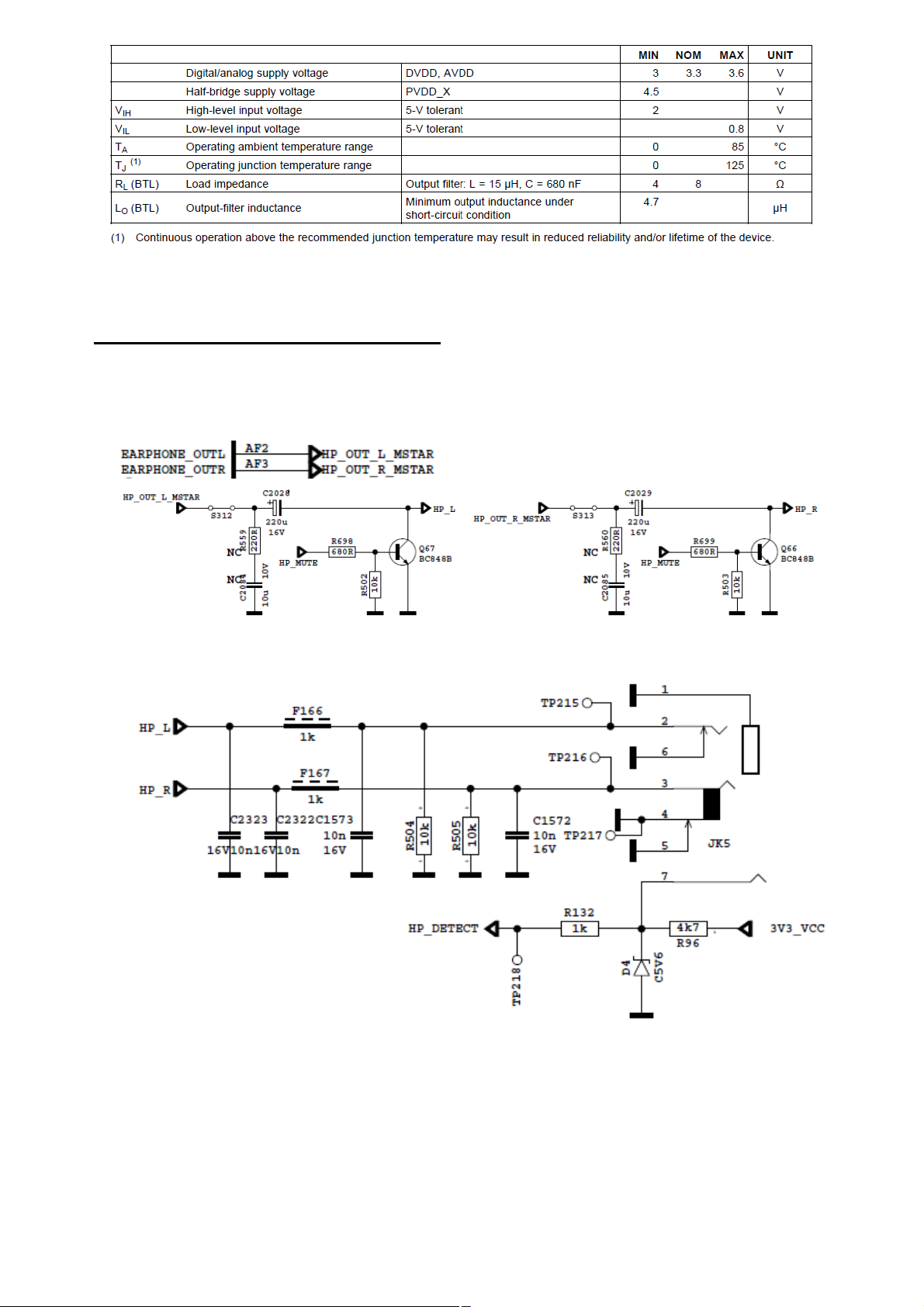
Table: Recommended Operating Conditions
B. HEAD-PHONE AMPLIFIER STAGE
Head-phone is a SoC (single on chip) configuration in mainboard, Design scheme is shown in figure 3.
10
Figure: Head-phone

C. SUBWOOFER AMPLIFIER STAGE
PREAMPLIFIER (DRV632)
Description
The DRV632 is a 2-VRMS pop-free stereo line driver designed to allow the removal of the output dcblocking capacitors for reduced component count and cost. The device is ideal for single-supply electronics
where size and cost are critical design parameters.
Designed using TI’s patented DirectPath™ technology, The DRV632 is capable of driving 2 VRMS into a
10-kΩ load with 3.3-V supply voltage. The device has differential inputs and uses external gain-setting resistors
to support a gain range of ±1 V/V to ±10 V/V, and gain can be configured individually for each channel. Line
outputs have ±8-kV IEC ESD protection, requiring just a simple resistor-capacitor ESD protection circuit. The
DRV632 has built-in active-mute control for pop-free audio on/off control. The DRV632 has an external
undervoltage detector that mutes the output when the power supply is removed, ensuring a pop-free shutdown.
Using the DRV632 in audio products can reduce component count considerably compared to traditional
methods of generating a 2-VRMS output. The DRV632 does not require a power supply greater than 3.3 V to
generate its 5.6-Vpp output, nor does it require a split-rail power supply. The DRV632 integrates its own charge
pump to generate a negative supply rail that provides a clean, pop-free ground-biased 2-VRMS output.
The DRV632 is available in a 14-pin TSSOP.
Features
Stereo DirectPath™ Audio Line Driver
o 2 Vrms Into 10 k With 3.3-V Supply
Low THD+N < 0.01% at 2 Vrms Into 10 k
High SNR, >90 dB
600- Output Load Compliant
Differential Input and Single-Ended Output
Adjustable Gain by External Gain-Setting Resistors
Low DC Offset, <1 mV
Ground-Referenced Outputs Eliminate DC-Blocking Capacitors
o Reduce Board Area
o Reduce Component Cost
o Improve THD+N Performance
o No Degradation of Low-Frequency Response Due to Output Capacitors
Short-Circuit Protection
Click- and Pop-Reduction Circuitry
External Undervoltage Mute
Active Mute Control for Pop-Free Audio On/Off Control
Space-Saving TSSOP Package
11
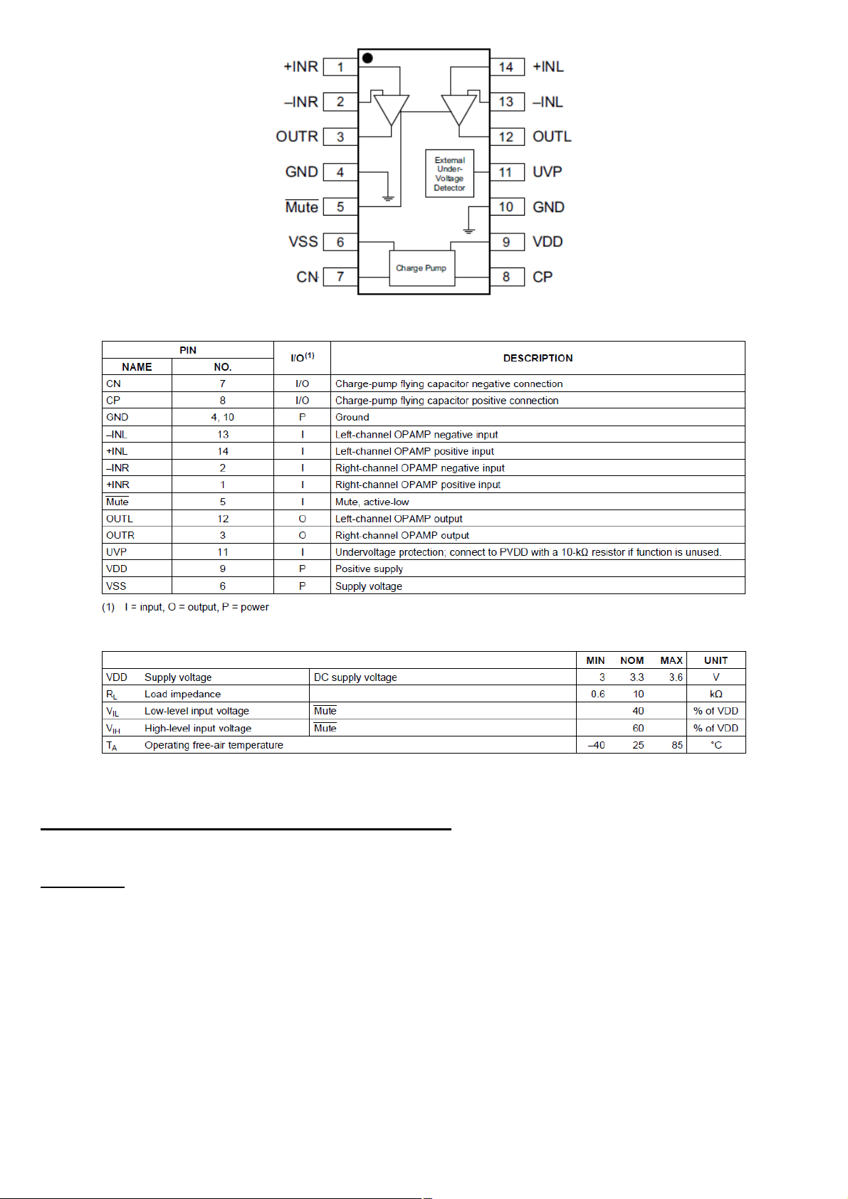
Figure: PW package
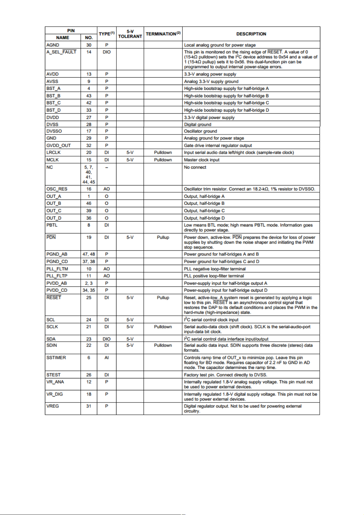
Table: Pin functions
Table: Recommended operating conditions
SUB WOOFER MAIN AMPLIFIER (TAS5727)
Description
The TAS5727 is a 25-W, efficient, digital-audio power amplifier for driving stereo bridge-tied
speakers.One serial data input allows processing of up to two discrete audio processors and MPEG decoders.
The device accepts a wide range of input data and data rates. A fully programmable data path routes these
channels to the internal speaker drivers.
The TAS5727 is a slave-only device receiving all clocks from external sources. The TAS5727 operates
with a PWM carrier between a 384-kHz switching rate amd a 288-kHz switching rate, depending on the input
sample rate. Oversampling combined with a fourth-order noise shaper provides a flat noise flor and excellent
dynamic range from 20 Hz to 20 Khz.
12

Features
Audio Input/Output
o 25 W Into an 8- Load From a 20-V Supply
o Wide PVDD Range, From 8V to 26V
o Supports BTL Configuration with 4- Load
o Efficient Class-D Operation Elminates Need for Heatsinks
o One serial Audio Input (Two Audio Channels)
2
o I
C Address Selection Pin (Chip Select)
o Single Output Filter PBTL Support
o Supports 441-kHz to 48-kHz Sample Rate (LJ/RJ/I
Audio/PWM Processing
o Indepent Channel Volume Control With Gain of 24 dB to Mute With 0.125-dB
Resolution Steps
o Programmable Two-Band Dynamic-Range Control
o 18 Programmable Biquads for Speaker EQ and Other Audio-Processing Features
o Programmable Coefficients for DRC Filters
o DC Blocking Filters
General Features
2
C Serial Control Interface Operational Without MCLK
o I
o Requires Only 3.3 V and PVDD
o No External Oscillator: Internal Oscillator for Automatic Rate Detection
o Surface-Mount, 48-Pin HTQFP Package
o Thermal and Short-Circuit Protection
o 106-dB SNR, A-Weighted
o AD,BD, and Ternary Modulation
o Up to 90% Efficient
o PWM Level Meter to Measure the Digital Power Profile
Benefits
o EQ: Speaker Equalization Improves Audio Performance
o Two-Band DRC: Dynamic Range Compression. Can Be Used As Power Limiter. Enables Speaker
Protection, Easy Listening, Night-Mode Listening
o Autodetect: Automatically Detects Sample-Rate Changes. No need for External Microprocessor
Intervention
Applications:
o LCD TV, LED TV, Soundbar
2
S)
13
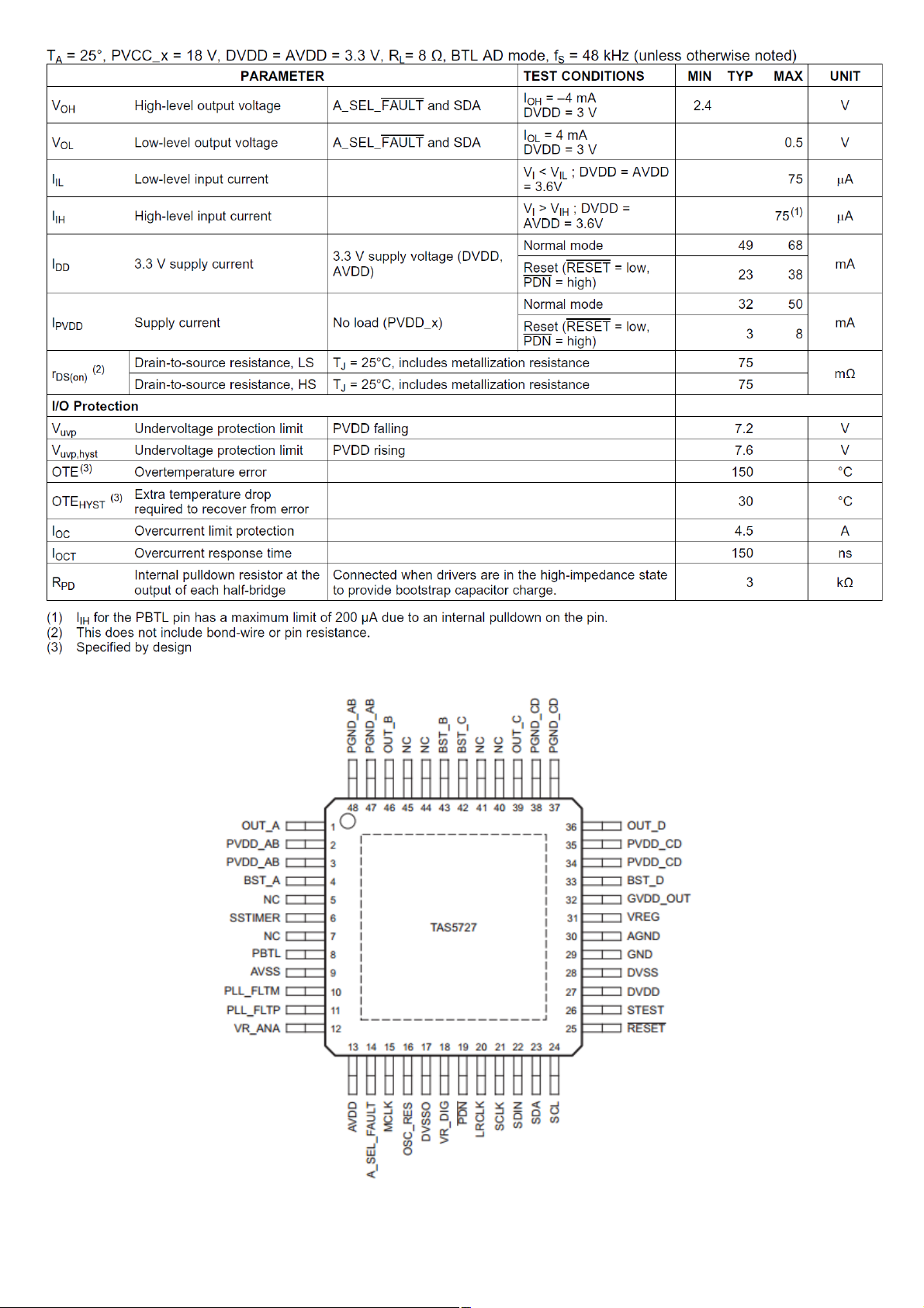
Table: Electrical Characteristics
14
Figure: PHP Package (Top View)
15
Table: Pin Functions
4. POWER STAGE
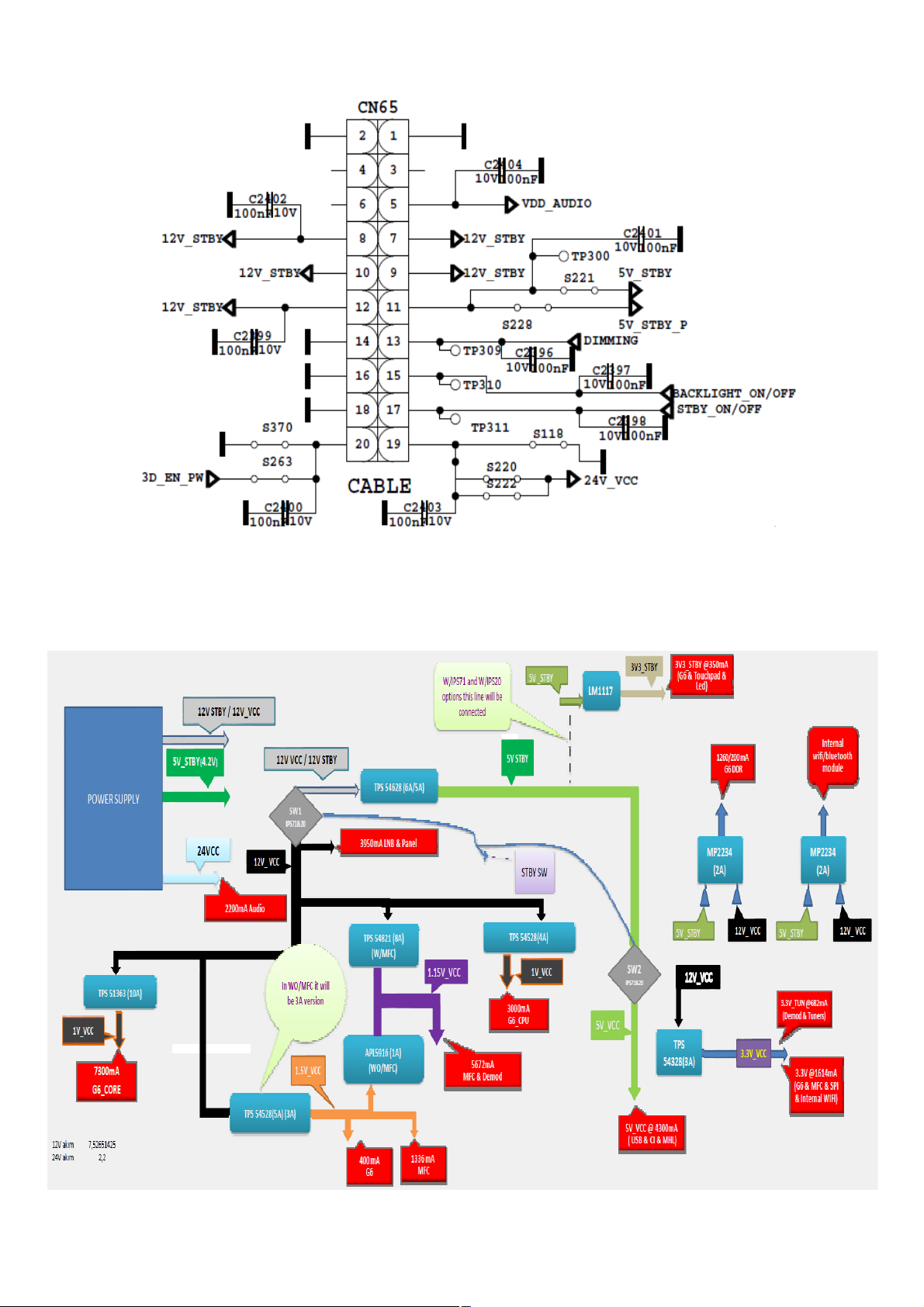
Figure: Power socket and options
Power socket is used for taking voltages which are 12V, 5V and 24V(VDD_Audio). These voltages are
produced in power board. Also socket is used for giving dimming, backlight and standby signals with power
board. It is shown in figure 7.
16
Figure: General illustration of voltage stages on main board

24V(VDD_Audio) goes directly to the audio side, through power socket other incoming voltages from
power card are converted several voltages, shown in figure 8.
List of the components are:
TPS54528
TPS54328
TPS54821
TPS51363
APL5910
LM1117
TPS54528
General Description
The TPS54528 is an adaptive on-time D-CAP2 mode synchronous buck converter.The TPS54528 enables
system designers to complete the suite of various end-equipment power bus regulators with a cost effective, low
component count, low standby current solution. The main control loop for the TPS54528 uses the D-CAP2
mode control that provides a fast transient response with no external compensation components. The adaptive
on-time control supports seamless transition between PWM mode at higher load conditions and Eco-mode
operation at light loads. Eco-mode allows the TSP54528 to maintain high efficiency during lighter load
conditions. The TPS54528 also has a proprietary circuit that enables the device to adopt to both low equivalent
series resistance (ESR)output capacitors, such as POSCAP or SP-CAP, and ultra-low ESR ceramic capacitors.
The device operates from 4.5-V to 18-V VIN input. The output voltage can be programmed between 0.76 V
and 6 V. The device also features an adjustable soft start time. The TPS54528 is available in the 8-pin DDA
package, and designed to operate from -40 C to 85 C.
Features
D-CAP2 Mode Enables Fast Transient Response
Low Output ripple and Allows Ceramic Output Capacitor
Wide V
Input Voltage Range: 4.5 V to 18 V
IN
Output Voltage Range: 0.76 V to 6 V
Highly Efficient Integrated FETs Optimized for Lower Duty Cycle Applications- 65 mOhm (High Side)
and 36 mOhm (Low Side)
High Efficiency, less than 10 mikroAmper at shutdown
High Initial Bandgap Reference Accuracy
Adjustable Soft Start
Pre-Biased Soft Start
650-kHz Switching Frequency (f
SW
)
Cycle By Cycle Over Current Limit
Auto-Skip Eco-mode for High Efficiency at Light Load
Applications
Wide Range of Applications for Low Voltage System
Digital TV Power Supply
High Definition Blu-ray Disc Players
17
Networking Home Terminal
Digital Set Top Box(STB)
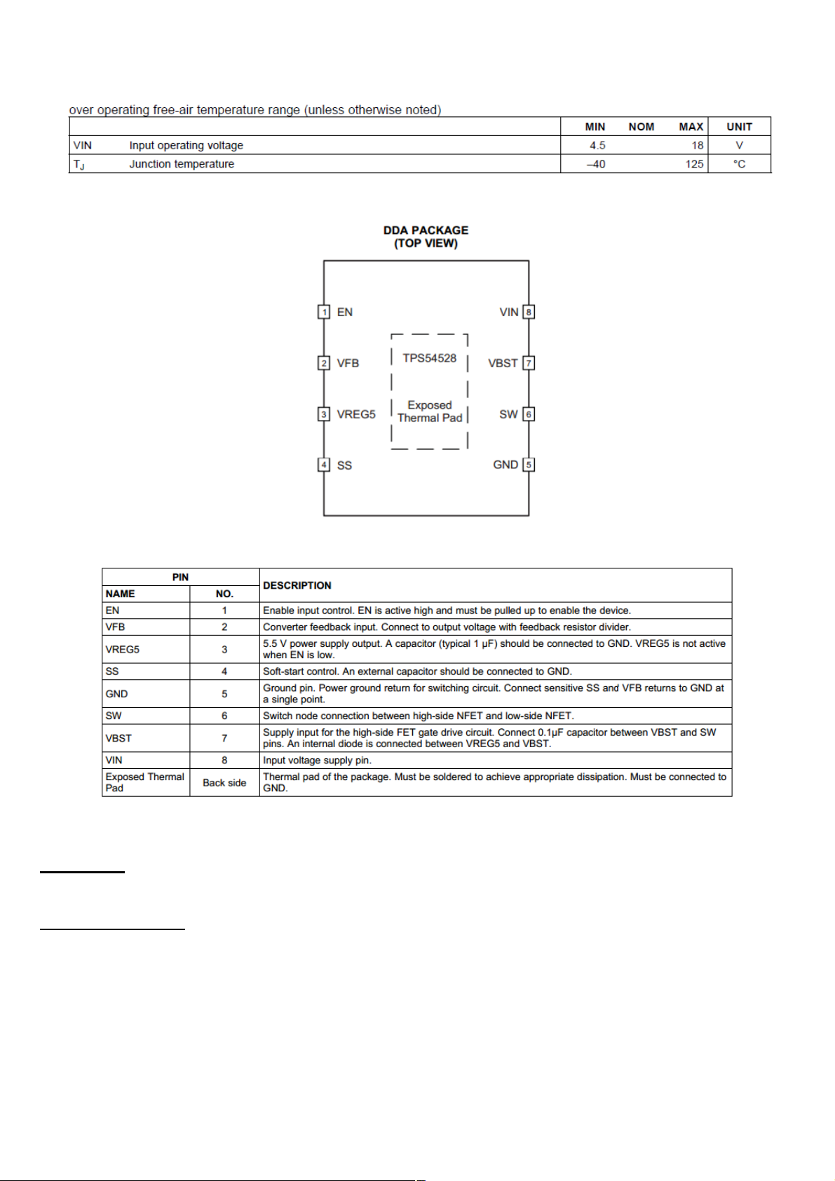
Table: Recommended operating conditions
Figure: Pin Description
Table: Pin functions
TPS54328
General Description
The TPS54328 is an adaptive on-time D-CAP2 mode synchronous buck converter.The TPS54328 enables
system designers to complete the suite of various end-equipment power bus regulators with a cost effective, low
component count, low standby current solution. The main control loop for the TPS54328 uses the D-CAP2
mode control that provides a fast transient response with no external compensation components. The adaptive
on-time control supports seamless transition between PWM mode at higher load conditions and Eco-mode
operation at light loads. Eco-mode allows the TSP54328 to maintain high efficiency during lighter load
conditions. The TPS54328 also has a proprietary circuit that enables the device to adopt to both low equivalent
18
series resistance (ESR)output capacitors, such as POSCAP or SP-CAP, and ultra-low ESR ceramic capacitors.
The device operates from 4.5-V to 18-V VIN input. The output voltage can be programmed between 0.76 V
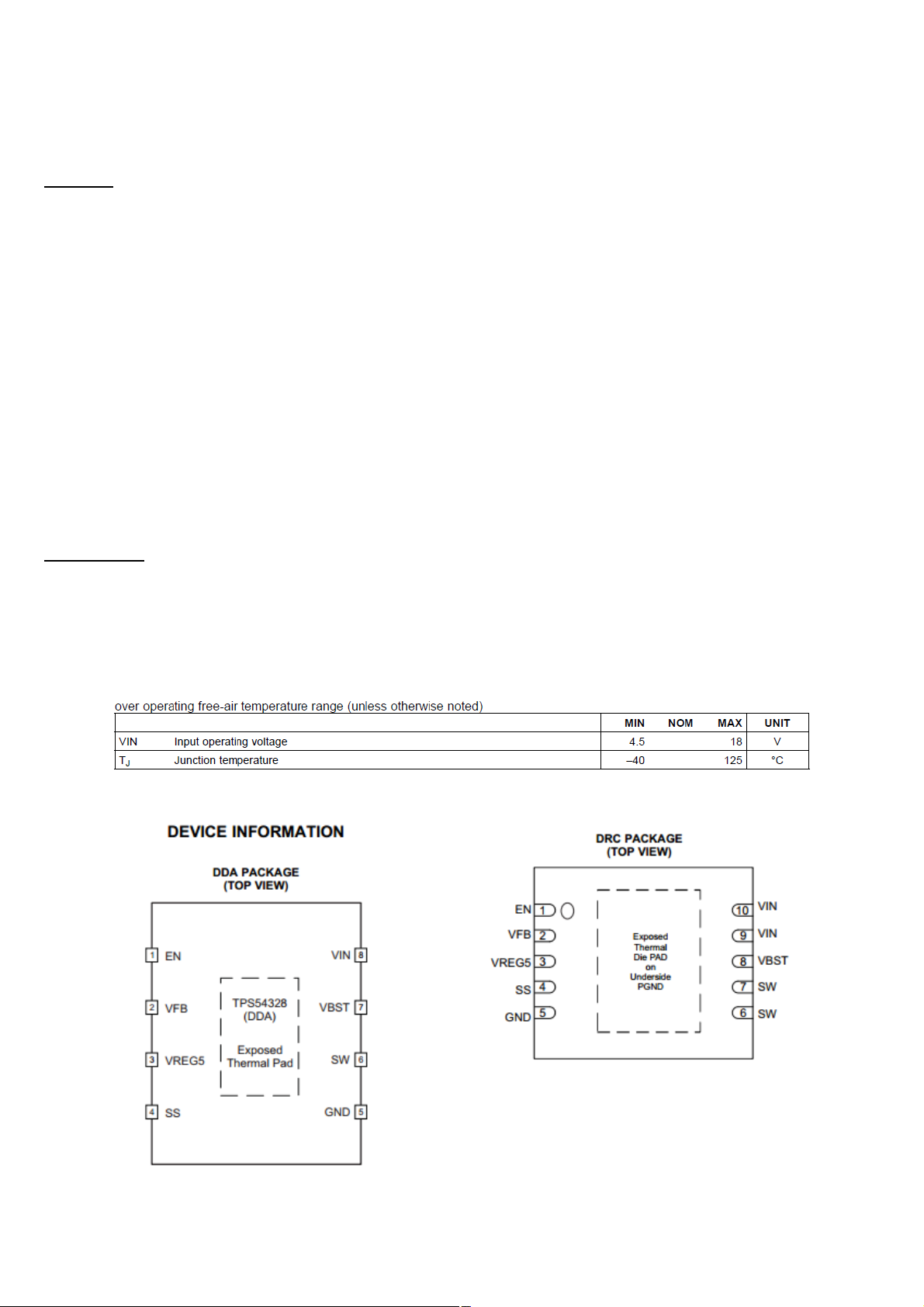
and 7 V. The device also features an adjustable soft start time. The TPS54328 is available in the 8-pin DDA and
10-pin DRC packages, and is designed to operate over the ambient temperature range of -40C to 85C.
Features
D-CAP2 Mode Enables Fast Transient Response
Low Output ripple and Allows Ceramic Output Capacitor
Wide V
Input Voltage Range: 4.5 V to 18 V
IN
Output Voltage Range: 0.76 V to 7 V
Highly Efficient Integrated FETs Optimized for Lower Duty Cycle Applications- 100 mOhm (High
Side) and 70 mOhm (Low Side)
High Efficiency, less than 10 mikroAmper at shutdown
High Initial Bandgap Reference Accuracy
Adjustable Soft Start
Pre-Biased Soft Start
700-kHz Switching Frequency (f
SW
)
Cycle By Cycle Over Current Limit
Auto-Skip Eco-mode for High Efficiency at Light Load
Applications
Wide Range of Applications for Low Voltage System
Digital TV Power Supply
High Definition Blu-ray Disc Players
Networking Home Terminal
Digital Set Top Box(STB)
Table: Recommended operating conditions
19
Figure: Pin Description
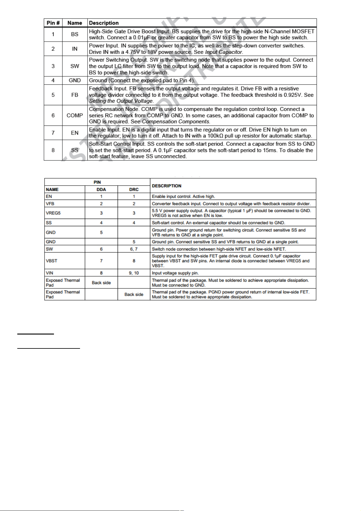
Table: Pin functions
Table: Pin description
TPS51363
General Description
The TPS51363 is a high-voltage input, synchronous converter with integrated FET, based on D-CAP2™
control topology, which enables fast transient response and supports both POSCAP and all MLCC output
capacitors. TI proprietary FET technology combined with TI leading-edge package technology provides the
highest density solution for single-output power rail such as VCCIO and VDDQ for DDR notebook memory, or
any point-of-load (POL) in wide application. The feature set includes switching frequency of 400 kHz and 800
kHz. Programmable soft-start time with an external capacitor. auto skip, pre-bias startup, integrated bootstrap
switch, power good, enable and a full suite of fault protection schemes, including OCL, UVP, OVP, 5-V UVLO
and thermal shutdown. It is packaged in 3.5 mm × 4.5 mm, 0.4-mm pitch, 28-pin QFN (RVE), and specified
from -10°C to 85°C.
20
Features
Input Voltage Range: 3 V to 22 V
Output Voltage Range: 0.6 V to 2 V
8-A or 10-A Integrated FET Converter
Fewest External Components
Soft-Start Time Programmable by External Capacitor
Switching Frequency: 400 kHz and 800 kHz
D-CAP2™ Architecture to Enable POSCAP and All MLCC Output Capacitor Usage
Integrated and Temperature Compensated Low-Side On-Resistance Sensing for Accurate OCL
Protection
Powergood Output OCL, OVP, UVP and UVLO Protections
Thermal Shutdown (non-latch)
Output Discharge Function Table 1. Current Ratings
Integrated Boost MOSFET Switch
28-Pin, 3.5-mm × 4.5-mm, RVE, QFN Package with 0.4-mm Pitch and 1-mm Height
Applications
• Notebook Computers (VCCIO)
• Memory Rails (DDR VDDQ)
21
Table: Recommended operating conditions
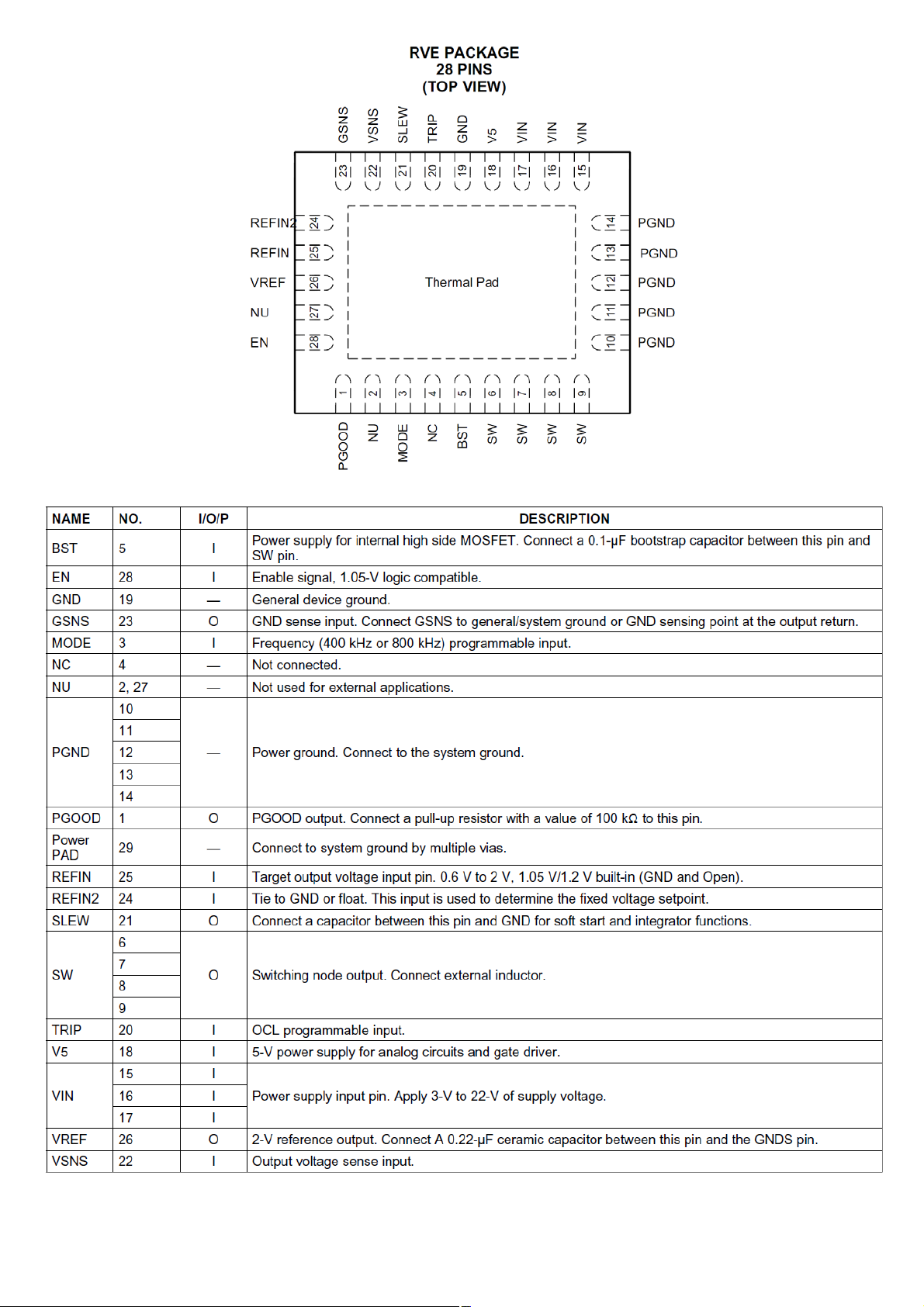
Figure: Pin Description
22
Table: Pin functions

TPS54821
General Description
The TPS54821 in thermally enhanced 3.5 mm x 3.5 mm QFN package is a full featured 17 V, 8 A
synchronous step down converter which is optimized for small designs through high efficiency and integrating
the high-side and low-side MOSFETs. Further space savings are achieved through current mode control, which
reduces component count, and by selecting a high switching frequency, reducing the inductor's footprint. The
output voltage startup ramp is controlled by the SS/TR pin which allows operation as either a stand alone power
supply or in tracking situations. Power sequencing is also possible by correctly configuring the enable and the
open drain power good pins. Cycle by cycle current limiting on the high-side FET protects the device in
overload situations and is enhanced by a low-side sourcing current limit which prevents current runaway. There
is also a low-side sinking current limit which turns off the low-side MOSFET to prevent excessive reverse
current. Hiccup protection will be triggered if the overcurrent condition has persisted for longer than the preset
time. Thermal hiccup protection disables the device when the die temperature exceeds the thermal shutdown
temperature and enables the part again after the built-in thermal shutdown hiccup time.
Features
Integrated 26 mΩ / 19 mΩ MOSFETs
Split Power Rail: 1.6 V to 17 V on PVIN
200 kHz to 1.6 MHz Switching Frequency
Synchronizes to External Clock
0.6V ±1% Voltage Reference Over Temperature
Low 2 μA Shutdown Quiescent Current
Monotonic Start-Up into Pre-biased Outputs
–40°C to 125°C Operating Junction Temperature Range
Adjustable Input Undervoltage Lockout
Adjustable Slow Start/Power Sequencing
Power Good Output Monitor for Undervoltage and Overvoltage
Adjustable Input Undervoltage Lockout
Applications
Digital TV Power Supplies
Set Top Boxes
Blu-ray DVDs
Home Terminals
23
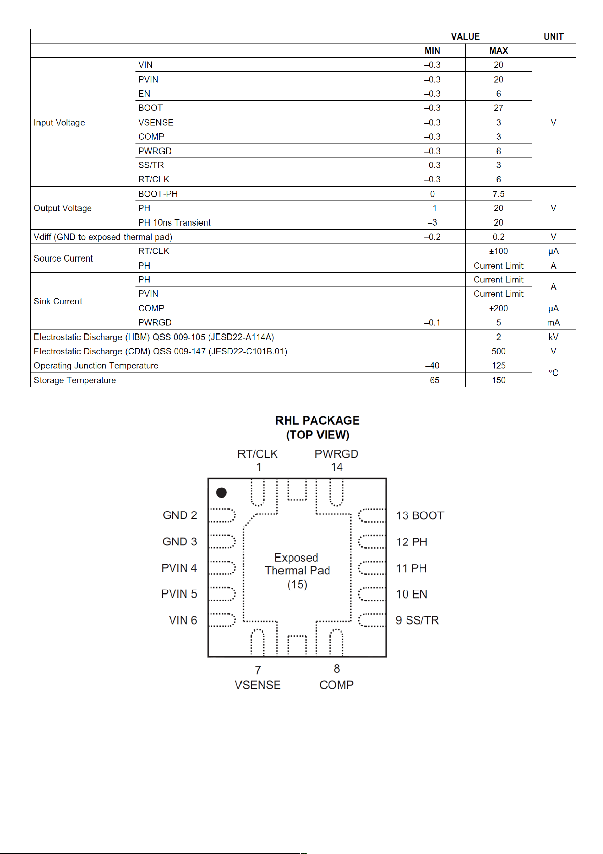
Table: Recommended operating conditions
24
Figure: Pin Description
 Loading...