

Page 1

15” TFT TV
SERVICE MANUAL
PDF created with FinePrint pdfFactory trial version http://www.pdffactory.com
Page 2

TABLE OF CONTENTS
1. INTRODUCTION...................................................................................................................................1
2. TUNER..................................................................................................................................................1
3. TDA988X...............................................................................................................................................1
4. MULTI STANDARD SOUND PROCESSOR ........................................................................................1
5. AUDIO AMPLIFIER STAGE WITH TDA7299.......................................................................................1
6. POWER.................................................................................................................................................2
7. MICROCONTROLLER SDA55XX ........................................................................................................2
7.1. General Features...............................................................................................................................2
7.2. External Crystal and Programmable Clock Speed............................................................................ 2
7.3. Microcontroller Features....................................................................................................................2
7.4. Memory..............................................................................................................................................2
7.5. Display Features................................................................................................................................2
7.6. ROM Characters................................................................................................................................2
7.7. Acquisition Features..........................................................................................................................3
7.8. Ports ..................................................................................................................................................3
8. SERIAL ACCESS CMOS 16K (2048*8) EEPROM ST24C16 ..............................................................3
9. CLASS AB STEREO HEADPHONE DRIVER TDA1308......................................................................3
10. SAW FILTERS ......................................................................................................................................3
11. IC DESCRIPTIONS AND INTERNAL BLOCK DIAGRAM....................................................................4
11.1. TEA5114A......................................................................................................................................4
11.1.1. General description..............................................................................................................4
11.1.2. Features.................................................................................................................................4
11.1.3. Pin Connections ...................................................................................................................4
11.2. MC34167........................................................................................................................................5
11.2.1. General Description..............................................................................................................5
11.2.2. Features.................................................................................................................................5
11.3. LM7808..........................................................................................................................................5
11.3.1. Description............................................................................................................................5
11.3.2. Features.................................................................................................................................5
11.4. SDA55XX.......................................................................................................................................6
11.4.1. General description..............................................................................................................6
11.5. TFMS5360 .....................................................................................................................................6
11.5.1. Description............................................................................................................................6
11.5.2. Features.................................................................................................................................6
11.6. SST37VF040..................................................................................................................................7
11.6.1. Description............................................................................................................................7
11.6.2. Features.................................................................................................................................7
11.6.3. Pin Description .....................................................................................................................7
11.7. ST24LC21......................................................................................................................................8
11.7.1. Description............................................................................................................................8
11.7.2. Features.................................................................................................................................8
11.7.3. Pin connections....................................................................................................................8
11.8. VPC3230D.....................................................................................................................................9
11.8.1. General Description..............................................................................................................9
11.8.2. Pin Connections and Short Descriptions........................................................................... 9
11.9. AL300...........................................................................................................................................11
11.9.1. General Description............................................................................................................11
11.9.2. Features...............................................................................................................................11
11.9.3. Pin Definition and Description ..........................................................................................11
11.10. LM1086........................................................................................................................................14
11.10.1. Description ..........................................................................................................................14
11.10.2. Features...............................................................................................................................14
11.10.3. Applications ........................................................................................................................14
11.10.4. Connection Diagrams.........................................................................................................14
11.11. LM1117........................................................................................................................................15
11.11.1. General Description............................................................................................................15
11.11.2. Features...............................................................................................................................15
i
i
15” TFT TV Service Manual 24/10/2003
PDF created with FinePrint pdfFactory trial version http://www.pdffactory.com
Page 3

11.11.3. Applications ........................................................................................................................15
11.11.4. Connection Diagrams.........................................................................................................15
11.12. TDA7299......................................................................................................................................16
11.12.1. Description ..........................................................................................................................16
11.12.2. Features...............................................................................................................................16
11.12.3. Pin Connection ...................................................................................................................16
11.13. DS90C385.................................................................................................................................... 17
11.13.1. General Description............................................................................................................17
11.13.2. Features...............................................................................................................................17
11.13.3. Pin Description ...................................................................................................................17
11.14. TDA1308......................................................................................................................................18
11.14.1. General Description............................................................................................................18
11.14.2. Features...............................................................................................................................18
11.14.3. Pinning.................................................................................................................................18
11.15. TL431...........................................................................................................................................19
11.15.1. Description ..........................................................................................................................19
11.15.2. Features...............................................................................................................................19
11.15.3. Pin Configurations..............................................................................................................19
11.16. 24C16........................................................................................................................................... 20
11.16.1. Description ..........................................................................................................................20
11.16.2. Features...............................................................................................................................20
11.16.3. Pin Configuration................................................................................................................20
11.16.4. Pin Description ...................................................................................................................20
11.17. AL875...........................................................................................................................................21
11.17.1. General Description............................................................................................................21
11.17.2. General Features ................................................................................................................21
11.17.3. Pin Definition and Description ..........................................................................................21
11.18. 74HC244A.................................................................................................................................... 23
11.18.1. Description ..........................................................................................................................23
11.18.2. General Features ................................................................................................................23
11.18.3. Pin Description ...................................................................................................................23
11.19. ICS1523.......................................................................................................................................24
11.19.1. Description ..........................................................................................................................24
11.19.2. Features...............................................................................................................................24
11.20. MC34063......................................................................................................................................25
11.20.1. Description ..........................................................................................................................25
11.20.2. Features...............................................................................................................................25
11.20.3. Pin connections ..................................................................................................................25
11.21. TDA9885/86.................................................................................................................................26
11.21.1. General description ............................................................................................................26
11.21.2. 13.13.2.Features..................................................................................................................26
11.21.3. 13.13.3.Pinning....................................................................................................................26
11.22. MSP34X0G..................................................................................................................................27
11.22.1. Introduction.........................................................................................................................27
11.22.2. Features...............................................................................................................................27
11.22.3. Pin connections ..................................................................................................................28
11.23. SAA3010T....................................................................................................................................30
11.23.1. 14.22.1.Description .............................................................................................................30
11.23.2. 14.22.2.Features..................................................................................................................30
11.23.3. 14.22.3.Pinning....................................................................................................................30
12. SERVICE MENU SETTINGS..............................................................................................................31
12.1. ADJUST MENU SETTINGS ........................................................................................................31
OPTIONS MENU SETTINGS.....................................................................................................................33
12.2. APS WSS TEST MENU............................................................................................................... 38
13. BLOCK DIAGRAM ..............................................................................................................................39
14. CIRCUIT DIAGRAMS .........................................................................................................................40
ii
ii
15” TFT TV Service Manual 24/10/2003
PDF created with FinePrint pdfFactory trial version http://www.pdffactory.com
Page 4

1. INTRODUCTION
TFT TV is a progressive scan flicker free colour television with PC input, driving a XGA panel with 4:3
aspect ratio. The chassis is capable of operation in PAL, SECAM, NTSC (playback) colour standards and
multiple transmission standards as B/G, D/K, I/I’, and L/L´. Sound system output is supplying 2x2W
(10%THD) for left and right outputs of 8Ω speakers. The chassis is equipped with one full SCART, one
front-AV, one SVHS, one D-Sub 15 (PC) input and one line out (left and right) and one HP outputs.
2. TUNER
The hardware and software of the TV is suitable for tuners, supplied by different companies, which are
selected from the Service Menu. These tuners can be combined VHF, UHF tuners suitable for CCIR
systems B/G, H, L, L´, I/I´, and D/K. The tuning is available through the digitally controlled I2C bus (PLL).
Below you will find info on one of the Tuners in use.
General description of UV1316:
The UV1316 tuner belongs to the UV 1300 family of tuners, which are designed to meet a wide range of
applications. It is a combined VHF, UHF tuner suitable for CCIR systems B/G, H, L, L’, I and I’. The low IF
output impedance has been designed for direct drive of a wide variety of SAW filters with sufficient
suppression of triple transient.
Features of UV1316:
1. Member of the UV1300 family small sized UHF/VHF tuners
2. Systems CCIR: B/G, H, L, L’, I and I’; OIRT: D/K
3. Digitally controlled (PLL) tuning via I2C-bus
4. Off-air channels, S-cable channels and Hyperband
5. World standardised mechanical dimensions and world standard pinning
6. Compact size
7. Complies to “CENELEC EN55020” and “EN55013”
Pinning:
1. Gain control voltage (AGC) : 4.0V, Max: 4.5V
2. Tuning voltage
3. I²C-bus address select : Max: 5.5V
4. I²C-bus serial clock : Min:-0.3V, Max: 5.5V
5. I²C-bus serial data : Min:-0.3V, Max: 5.5V
6. Not connected
7. PLL supply voltage : 5.0V, Min: 4.75V, Max: 5.5V
8. ADC input
9. Tuner supply voltage : 33V, Min: 30V, Max: 35V
10. Symmetrical IF output 1
11. Symmetrical IF output 2
3. TDA988X
The TDA9885 is an alignment-free single standard (without positive modulation) vision and sound IF signal
PLL.
The TDA9886 is an alignment-free multistandard (PAL, SECAM and NTSC) vision and sound IF signal
PLL demodulator for positive and negative modulation including sound AM and FM processing.
Both devices can be used for TV, VTR, PC and set-top box applications.
4. MULTI STANDARD SOUND PROCESSOR
The MSP 34x0G family of single-chip Multistandard Sound Processors covers the sound processing of all
analog TV-Standards worldwide, as well as the NICAM digital sound standards. The full TV sound
processing, starting with analog sound IF signal-in, down to processed analog AF-out, is performed on a
single chip. Signal conforming to the standard by the Broadcast Television Systems Committee (BTSC).
The DBX noise reduction, or alternatively, MICRONAS Noise Reduction (MNR) is performed alignment
free. Other processed standards are the Japanese FM-FM multiplex standard (EIA-J) and the FM Stereo
Radio standard.
5. AUDIO AMPLIFIER STAGE WITH TDA7299
The TDA7299 is an audio class-AB amplifier assembled in SO package specially designed for sound cards
application. By utilizing two TDA7299, chassis operates as a stereo TV set. TDA7299 has stand-by feature
1
1
15” TFT TV Service Manual 24/10/2003
PDF created with FinePrint pdfFactory trial version http://www.pdffactory.com
Page 5

for low stand-by power consumption by using pin #3. It can deliver 2W without clipping at 12V/8Ω
applications.
6. POWER
MC34167 is a power switch regulator, which can output 5V from 12V up to 5A. Utilising a power MOSFET
inside works at a very high efficiency without producing excessive heat. This IC is the main supply for the
voltages used in the main board. Using the pin 5 (stand-by) of IC, TFT TV can have low stand-by power
consumption.
7. MICROCONTROLLER SDA55XX
7.1. General Features
• Feature selection via special function register
• Simultaneous reception of TTX, VPS, PDC, and WSS (line 23)
• Supply Voltage 2.5 and 3.3 V
• ROM version is used.
7.2. External Crystal and Programmable Clock Speed
• Single external 6MHz crystal, all necessary clocks are generated internally
• CPU clock speed selectable via special function registers.
• Normal Mode 33.33 MHz CPU clock, Power Save mode 8.33 MHz
7.3. Microcontroller Features
• 8bit 8051 instruction set compatible CPU.
• 33.33-MHz internal clock (max.)
• 0.360 ms (min.) instruction cycle
• Two 16-bit timers
• Watchdog timer
• Capture compare timer for infrared remote control decoding
• Pulse width modulation unit (2 channels 14 bit, 6 channels 8 bit)
• ADC (4 channels, 8 bit)
• UART(rxd,txd)
7.4. Memory
• Up to 128 Kilobyte on Chip Program ROM
• Eight 16-bit data pointer registers (DPTR)
• 256-bytes on-chip Processor Internal RAM (IRAM)
• 128bytes extended stack memory.
• Display RAM and TXT/VPS/PDC/WSS-Acquisition-Buffer directly accessible via MOVX
• UP to 16KByte on Chip Extended RAM (XRAM) consisting of;
- 1 Kilobyte on-chip ACQ-buffer-RAM (access via MOVX)
- 1 Kilobyte on-chip extended-RAM (XRAM, access via MOVX) for user software
- 3 Kilobyte Display Memory
7.5. Display Features
• ROM Character set supports all East and West European Languages in single device
• Mosaic Graphic Character Set
• Parallel Display Attributes
• Single/Double Width/Height of Characters
• Variable Flash Rate
• Programmable Screen Size (25 Rows x 33...64 Columns)
• Flexible Character Matrixes (HxV) 12 x 9...16
• Up to 256 Dynamical Redefinable Characters in standard mode; 1024 Dynamical Redefinable Characters
in Enhanced Mode
• CLUT with up to 4096 colour combinations
• Up to 16 Colours per DRCS Character
• One out of 8 Colours for Foreground and Background Colours for 1-bit DRCS and ROM Characters
7.6. ROM Characters
• Shadowing
2
2
15” TFT TV Service Manual 24/10/2003
PDF created with FinePrint pdfFactory trial version http://www.pdffactory.com
Page 6

• Contrast Reduction
• Pixel by Pixel Shiftable Cursor With up to 4 Different Colours
• Support of Progressive Scan and 100 Hz.
• 3 X 4Bits RGB-DACs On-Chip
• Free Programmable Pixel Clock from 10 MHz to 32MHz
• Pixel Clock Independent from CPU Clock
• Multinorm H/V-Display Synchronisation in Master or Slave Mode
7.7. Acquisition Features
• Multistandard Digital Data Slicer
• Parallel Multi-norm Slicing (TTX, VPS, WSS, CC, G+)
• Four Different Framing Codes Available
• Data Caption only limited by available Memory
• Programmable VBI-buffer
• Full Channel Data Slicing Supported
• Fully Digital Signal Processing
• Noise Measurement and Controlled Noise Compensation
• Attenuation Measurement and Compensation
• Group Delay Measurement and Compensation
• Exact Decoding of Echo Disturbed Signals
7.8. Ports
• One 8-bit I/O-port with open drain output and optional I 2 C Bus emulation support (Port0)
• Two 8-bit multifunction I/O-ports (Port1, Port3)
• One 4-bit port working as digital or analogue inputs for the ADC (Port2)
• One 2-bit I/O port with secondary function (P4.2, 4.3, 4.7)
• One 4-bit I/O-port with secondary function (P4.0, 4.1, 4.4) (Not available in P-SDIP 52)
8. SERIAL ACCESS CMOS 16K (2048*8) EEPROM ST24C16
The ST24C16 is an 16Kbit electrically erasable programmable memory (EEPROM), organised as 8 blocks
of 256*8 bits. The memory is compatible with the I²C standard, two wire serial interface, which uses a bidirectional data bus and serial clock. The memory carries a built-in 4 bit, unique device identification code
(1010) corresponding to the I²C bus definition. This is used together with 1 chip enable input (E) so that up
to 2*8K devices may be attached to the I²C bus and selected individually.
9. CLASS AB STEREO HEADPHONE DRIVER TDA1308
The TDA1308 is an integrated class AB stereo headphone driver contained in a DIP8 plastic package. The
device is fabricated in a 1 mm CMOS process and has been primarily developed for portable digital audio
applications.
10. SAW FILTERS
K3953M is an IF Filter for Video Applications. The package is SIP5K. Supported standards are B/G, D/K, I,
L/L’.
K9656M is an IF Filter for Audio Applications. The package is SIP5K. Supported standards are B/G, D/K, I,
L/L’.
3
3
15” TFT TV Service Manual 24/10/2003
PDF created with FinePrint pdfFactory trial version http://www.pdffactory.com
Page 7
11. IC DESCRIPTIONS AND INTERNAL BLOCK DIAGRAM
TEA5114A DS90C385
MC34167 TDA1308T
LM7808 TL431
SDA55XX 24C16
TFMS5360 AL875
SST37VF040 74HC244A
ST24LC21 ICS1523
VPC3230D MC34063
AL300 TDA9885/86
LM1086 MSP3400G
LM1117 SAA3010T
TDA7299
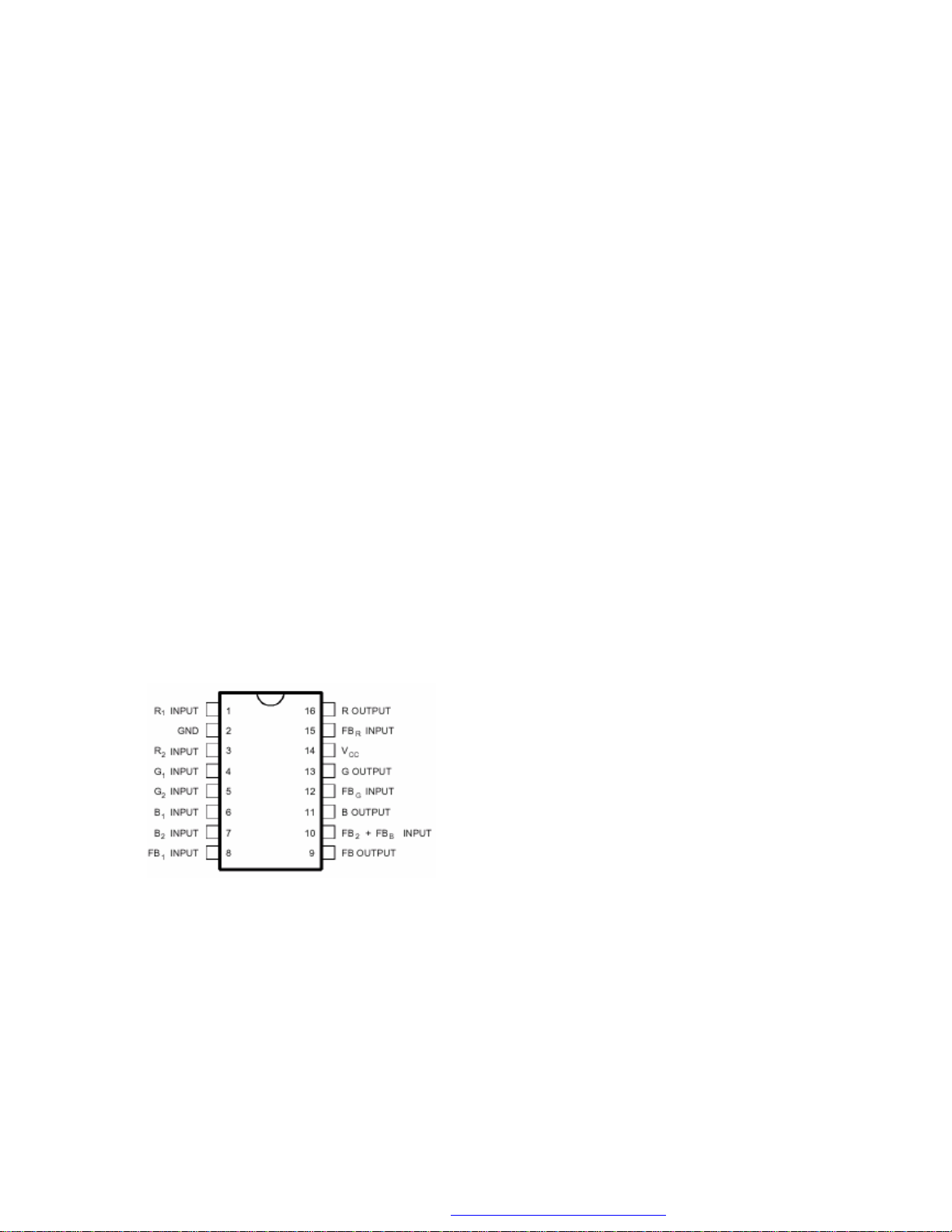
11.1. TEA5114A
11.1.1. General description
This integrated circuit provides RGB switching allowing connections between peri TV plug, internal RGB
generator and video processor in a TV set.
The input signal black level is tied to the same reference voltage on each input in order to have no
differential voltage when switching two RGB generators.
An AC output signal higher than 2 Vpp makes gain going slowly down to 0dBto protect the TV set video
amplifier from saturation.
Fast blanking output is a logical OR between FB1 (Pin 8) and FB2 (Pin 10).
11.1.2. Features
• 25MHz Bandwidth
• Crosstalk : 55dB
• Short circuit to ground or VCC protected
• Anti saturation gain changing
• Video switching
11.1.3. Pin Connections
4
4
15” TFT TV Service Manual 24/10/2003
PDF created with FinePrint pdfFactory trial version http://www.pdffactory.com
Page 8

11.2. MC34167
11.2.1. General Description
The MC34167, MC33167 series are high performance fixed frequency power switching regulators that
contain the primary functions required for dc–to–dc converters. This series was specifically designed to be
incorporated in step–down and voltage–inverting configurations with a minimum number of external
components and can also be used cost effectively in step–up applications.
These devices consist of an internal temperature compensated reference, fixed frequency oscillator with
on–chip timing components, latching pulse width modulator for single pulse metering, high gain error
amplifier, and a high current output switch.
Protective features consist of cycle–by–cycle current limiting, under voltage lockout, and thermal
shutdown. Also included is a low power standby mode that reduces power supply current to 36 mA.
11.2.2. Features
• Output Switch Current in Excess of 5.0 A
• Fixed Frequency Oscillator (72 kHz) with On–Chip Timing
• Provides 5.05 V Output without External Resistor Divider
• Precision 2% Reference
• 0% to 95% Output Duty Cycle
• Cycle–by–Cycle Current Limiting
• Under voltage Lockout with Hysteresis
• Internal Thermal Shutdown
• Operation from 7.5 V to 40 V
• Standby Mode Reduces Power Supply Current to 36 mA
• Economical 5–Lead TO–220 Package with Two Optional Leadforms
• Also Available in Surface Mount D 2 PAK Package
• Moisture Sensitivity Level (MSL) Equals 1
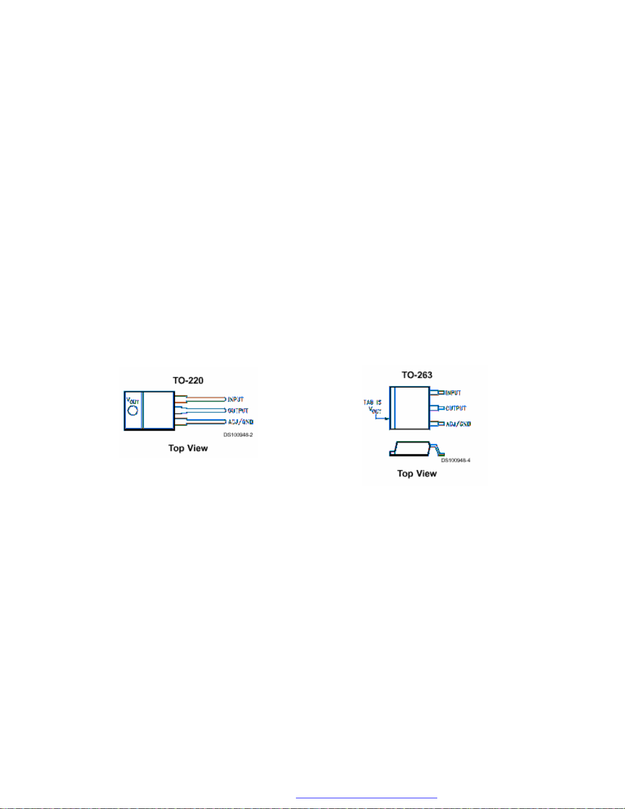
11.3. LM7808
11.3.1. Description
The L7800 series of three-terminal positive regulators is available in TO-220 TO-220FP TO-3 and D 2 PAK
packages and several fixed output voltages, making it useful in a wide range of applications. These
regulators can provide local on-card regulation, eliminating the distribution problems associated with single
point regulation. Each type employs internal current limiting, thermal shutdown and safe area protection,
making it essentially indestructible. If adequate heat sinking is provided, they can deliver over 1A output
current. Although designed primarily as fixed voltage regulators, these devices can be used with external
components to obtain adjustable voltages and currents.
11.3.2. Features
• Output Current Up To 1.5 A
• Output Voltages of 5; 5.2; 6; 8; 8.5; 9; 12; 15; 18; 24V
• Thermal Over load protection
• Short Circuit Protection
• Output Transition SOA Protection
5
5
15” TFT TV Service Manual 24/10/2003
PDF created with FinePrint pdfFactory trial version http://www.pdffactory.com
Page 9

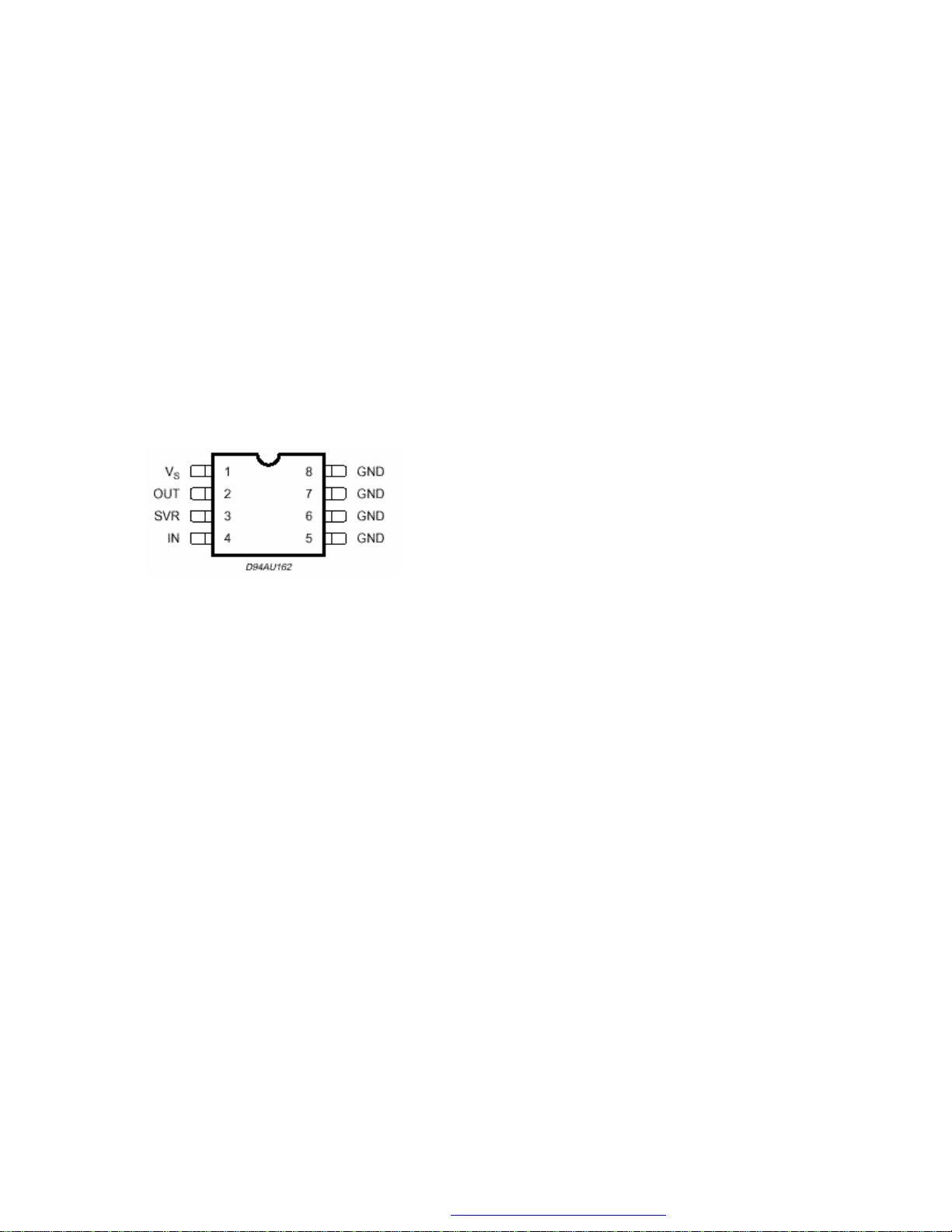
11.4. SDA55XX
11.4.1. General description
The SDA55XX is a single chip teletext decoder for decoding World System Teletext data as well as Video
Programming System (VPS), Program Delivery Control (PDC), and Wide Screen Signalling (WSS) data
used for PAL plus transmissions (Line 23). The device also supports Closed caption acquisition and
decoding. The device provides an integrated general-purpose, fully 8051-compatible Microcontroller with
television specific hardware features. Microcontroller has been enhanced to provide powerful features such
as memory banking, data pointers, and additional interrupts etc. The on-chip display unit for displaying
Level 1.5 teletext data can also be used for customer defined on screen displays. Internal XRAM consists
of up to16 Kbytes. Device has an internal ROM of up to 128 KBytes. ROMless versions can access up to 1
MByte of external RAM and ROM. The SDA 55XX supports a wide range of standards including PAL,
NTSC and contains a digital slicer for VPS, WSS, PDC, TTX and Closed Caption, an accelerating
acquisition hardware module, a display generator for Level 1.5 TTX data and powerful On screen Display
capabilities based on parallel attributes, and Pixel oriented characters (DRCS).
The 8-bit Microcontroller runs at 360 ns. cycle time (min.). Controller with dedicated hardware does most of
the internal TTX acquisition processing, transfers data to/from external memory interface and receives/
transmits data via I2C-firmware user-interface. The slicer combined with dedicated hardware stores TTX
data in a VBI buffer of 1 Kilobyte. The Microcontroller firmware performs all the acquisition tasks (hamming
and parity-checks, page search and evaluation of header control bits) once per field. Additionally, the
firmware can provide high-end Teletext features like Packet-26-handling, FLOF, TOP and list-pages. The
interface to user software is optimized for minimal overhead. SDA 55XX is realized in 0.25 micron
technology with 2.5 V supply voltage and 3.3 V I/O (TTL compatible). The software and hardware
development environment (TEAM) is available to simplify and speed up the development of the software
and On Screen Display. TEAM stands for TVT Expert Application Maker. It improves the TV controller
software quality in following aspects:
– Shorter time to market
– Re-usability
– Target independent development
– Verification and validation before targeting
– General test concept
– Graphical interface design requiring minimum programming and controller know how.
– Modular and open tool chain, configurable by customer.
11.5. TFMS5360
11.5.1. Description
The TFMS5360 is a miniature receiver for infrared remote control systems.
11.5.2. Features
• Photo detector and preamplifier in one.
• 36 KHZ
• Pin diode and preamp
• IR filter.
6
6
15” TFT TV Service Manual 24/10/2003
PDF created with FinePrint pdfFactory trial version http://www.pdffactory.com
Page 10
11.6. SST37VF040
11.6.1. Description
The SST37VF512/010/020/040 devices are 64K x8 / 128Kx8 / 256K x8 / 512K x8 CMOS, Many-Time
Programmable (MTP), low cost flash, manufactured with SST’s proprietary, high performance CMOS
SuperFlash technology. The split-gate cell design and thick oxide tunneling injector attain better reliability
and manufacturability compared with alternate approaches. The SST37VF512/010/020/040 can be
electrically erased and programmed at least 1000 times using an external programmer, e.g., to change the
contents of devices in inventory. The SST37VF512/010/020/040 have to be erased prior to programming.
These devices conform to JEDEC standard pinouts for byte-wide flash memories. Featuring high
performance Byte-Program, the SST37VF512/010/020/040 provide a typical Byte-Pro-gram time of 10 µs.
Designed, manufactured, and tested for a wide spectrum of applications, these devices are offered with an
endurance of at least 1000 cycles. Data retention is rated at greater than 100 years. The
SST37VF512/010/020/040 are suited for applications that require infrequent writes and low power
nonvolatile storage. These devices will improve flexibility, efficiency and performance while matching the
low cost in nonvolatile applications that currently use UV-EPROMs, OTPs, and mask ROMs.
11.6.2. Features
• Organized as 64K x8 / 128K x8 / 256K x8 / 512K x8
• 2.7-3.6V Read Operation
• Superior Reliability
– Endurance: At least 1000 Cycles
– Greater than 100 years Data Retention
• Low Power Consumption:
– Active Current: 10 mA (typical)
– Standby Current: 2 µA (typical)
• Fast Read Access Time:
– 70 ns, 90 ns
• Latched Address and Data
• Fast Byte-Program Operation:
– Byte-Program Time: 10 µs (typical)
– Chip Program Time:
0.6 seconds (typical) for SST37VF512
1.2 seconds (typical) for SST37VF010
2.4 seconds (typical) for SST37VF020
4.8 seconds (typical) for SST37VF040
• Electrical Erase Using Programmer
– Does not require UV source
– Chip-Erase Time: 100 ms (typical)
• CMOS I/O Compatibility
• JEDEC Standard Byte-wide Flash EEPROM Pinouts
• Packages Available
– 32-lead PLCC
– 32-lead TSOP (8mm x 14mm)
– 32-pin PDIP
11.6.3. Pin Description
Symbol Pin name Functions
1
A
-A0 Address Inputs To provide memory addresses.
MS
DQ7-DQ0
CE# Chip Enable
WE# Write Enable To program or erase (WE# = VIL pulse during Program or Erase)
OE# Output Enable To gate the data output buffers during Read operation when low
V
DD
V
SS
NC No Connection Unconnected pins.
1. AMS = Most significant address
AMS = A15 for SST37VF512, A16 for SST37VF010, A17 for SST37VF020, and A18 for SST37VF040
Data Input/output To output data during Read cycles and receive input data during Program
Power Supply To provide 3.0V supply (2.7-3.6V)
Ground
cycles. The outputs are in tri-state when OE# or CE# is high.
To activate the device when CE# is low.
7
7
15” TFT TV Service Manual 24/10/2003
PDF created with FinePrint pdfFactory trial version http://www.pdffactory.com
Page 11
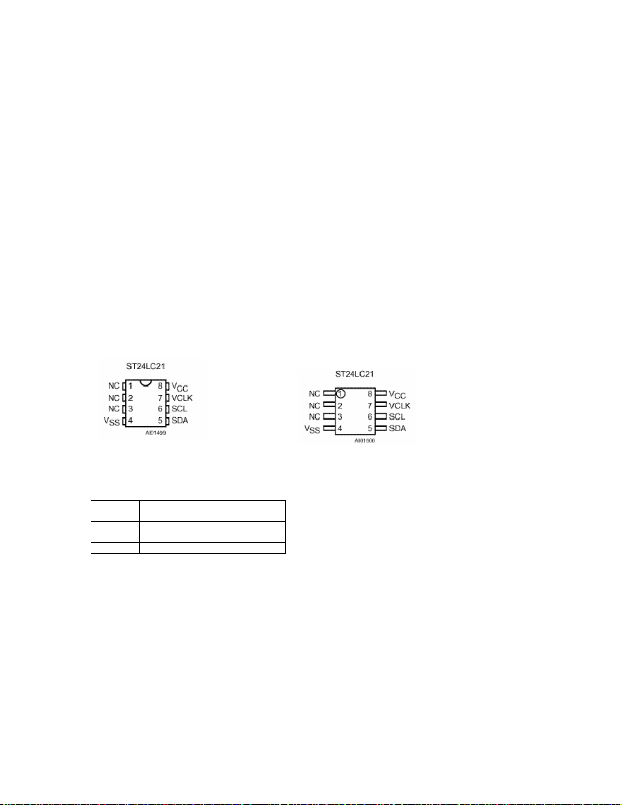
11.7. ST24LC21
11.7.1. Description
The ST24LC21 is a 1K bit electrically erasable programmable memory (EEPROM), organized by 8 bits.
This device can operate in two modes: Transmit Only mode and I2C bidirectional mode. When powered,
the device is in Transmit Only mode with EEPROM data clocked out from the rising edge of the signal
applied on VCLK. The device will switch to the I2C bidirectional mode upon the falling edge of the signal
applied on SCL pin. The ST24LC21 can not switch from the I2C bidirectional mode to the Transmit Only
mode (except when the power supply is removed). The device operates with a power supply value as low
as 2.5V. Both Plastic Dual-in-Line and Plastic Small Outline packages are available.
11.7.2. Features
• 1 million Erase/Write cycles
• 40 years data retention
• 2.5V To 5.5V single supply voltage
• 400k Hz compatibility over the full range of supply voltage
• Two wire serial interface I2C bus compatible
• Page Write (Up To 8 Bytes)
• Byte, random and sequential read modes
• Self timed programming cycle
• Automatic address incrementing
• Enhanced ESD/Latch up
• Performances
11.7.3. Pin connections
DIP Pin connections CO Pin connections
NC: Not connected
Signal names
SDA Serial data Address Input/Output
SCL Serial Clock (I2C mode)
Vcc Supply voltage
Vss Ground
VCLK Clock transmit only mode
8
8
15” TFT TV Service Manual 24/10/2003
PDF created with FinePrint pdfFactory trial version http://www.pdffactory.com
Page 12
11.8. VPC3230D
11.8.1. General Description
The VPC 323xD is a high-quality, single-chip video front-end, which is targeted for 4:3 and 16:9, 50/60-Hz
and 100/120 Hz TV sets. It can be combined with other members of the DIGIT3000 IC family (such as
DDP 331x) and/or it can be used with 3rd-party products.
The main features of the VPC 323xD are
• high-performance adaptive 4H comb filter Y/C separator with adjustable vertical peaking
• multi-standard colour decoder PAL/NTSC/SECAM including all substandards
• four CVBS, one S-VHS input, one CVBS output
• two RGB/YCr Cb component inputs, one Fast Blank (FB) input
• integrated high-quality A/D converters and associated clamp and AGC circuits
• multi-standard sync processing
• linear horizontal scaling (0.25 ... 4), as well as non-linear horizontal scaling ‘Panorama-vision’
• PAL+ preprocessing
• line-locked clock, data and sync, or 656-output interface
• peaking, contrast, brightness, color saturation and tint for RGB/ YC r C b and CVBS/ S-VHS
• high-quality soft mixer controlled by Fast Blank
• PIP processing for four picture sizes (1/4, 1/9, 1/16 or 1/36 of normal size) with 8-bit resolution
• 15 predefined PIP display configurations and expert mode (fully programmable)
• control interface for external field memory
• I2C-bus interface
• one 20.25-MHz crystal, few external components
• 80-pin PQFP package
11.8.2. Pin Connections and Short Descriptions
NC = not connected
LV = if not used, leave vacant
X = obligatory; connect as described in circuit diagram
SUPPLYA = 4.75...5.25 V, SUPPLYD = 3.15...3.45 V
Pin No.
PQFP
80-pin
1 B1/CB1IN IN VREF Blue1/Cb1 Analog Component Input
2 G1/Y1IN IN VREF Green1/Y1 Analog Component Input
3 R1/CR1IN IN VREF Read1/Cr1 Analog Component Input
4 B2/CB2IN IN VREF Blue2/Cb2 Analog Component Input
5 G2/Y2IN IN VREF Green2/Y2 Analog Component Input
6 R2/CR2IN IN VREF Read2/Cr2 Analog Component Input
7 ASGF X Analog Shield GNDF
8 FFRSTWIN IN LV or GNDD FIFO Reset Write Input
9 V
10 V
11 GNDD SUPPLYD X Ground, Digital Circuitry
12 GND
13 SCL IN/OUT X I2C Bus Clock
14 SDA IN/OUT X I2C Bus Data
15 RESQ IN X Reset Input, Active Low
16 TEST IN GNDD Test Pin, connect to GNDD
17 VGAV IN GNDD VGAV Input
18 YCOEQ IN GNDD Y/C Output Enable Input, Active Low
19 FFIE OUT LV FIFO Input Enable
20 FFWE OUT LV FIFO Write Enable
21 FFRSTW OUT LV FIFO Reset Write/Read
22 FFRE OUT LV FIFO Read Enable
23 FFOE OUT LV FIFO Output Enable
24 CLK20 IN/OUT LV Main Clock output 20.25 MHz
25 GNDPA OUT X Pad Decoupling Circuitry GND
26 V
27 LLC2 OUT LV Double Clock Output
28 LLC1 IN/OUT LV Clock Output
Pin Name Type Connection
OUT X Digital Decoupling Circuitry Supply Voltage
SUPCAP
SUPPLYD X Supply Voltage, Digital Circuitry
SUPD
OUT X Digital Decoupling Circuitry GND
CAP
OUT X Pad Decoupling Circuitry Supply Voltage
SUPPA
(if not used)
Short Description
9
9
15” TFT TV Service Manual 24/10/2003
PDF created with FinePrint pdfFactory trial version http://www.pdffactory.com
Page 13
29 V
30 GND
SUPPLYD X Supply Voltage, LLC Circuitry
SUPLLC
SUPPLYD X Ground, LLC Circuitry
LLC
31 Y7 OUT GNDY Picture Bus Luma (MSB)
32 Y6 OUT GNDY Picture Bus Luma
33 Y5 OUT GNDY Picture Bus Luma
34 Y4 OUT GNDY Picture Bus Luma
35 GNDY SUPPLYD X Ground, Luma Output Circuitry
36 V
SUPPLYD X Supply Voltage, Luma Output Circuitry
SUPY
37 Y3 OUT GNDY Picture Bus Luma
38 Y2 OUT GNDY Picture Bus Luma
39 Y1 OUT GNDY Picture Bus Luma
40 Y0 OUT GNDY Picture Bus Luma (LSB)
41 C7 OUT GNDC Picture Bus Chroma (MSB)
42 C6 OUT GNDC Picture Bus Chroma
43 C5 OUT GNDC Picture Bus Chroma
44 C4 OUT GNDC Picture Bus Chroma
45 V
SUPPLYD X Supply Voltage, Chroma Output Circuitry
SUPC
46 GNDC SUPPLYD X Ground, Chroma Output Circuitry
47 C3 OUT GNDC Picture Bus Chroma
48 C2 OUT GNDC Picture Bus Chroma
49 C1 OUT GNDC Picture Bus Chroma
50 C0 OUT GNDC Picture Bus Chroma (LSB)
51 GNDSY SUPPLYD X Ground Sync Pad Circuitry
52 V
SUPPLYD X Supply Voltage, Sync Pad Circuitry
SUPSY
53 INTLC OUT LV Interlace Output
54 AVO OUT LV Active Video Output
55 FSY/HC/HSYA OUT LV Front Sync/ Horizontal Clamp Pulse/Front-End
Horizontal Sync Output
56 MSY/HS IN/OUT LV Main Sync/Horizontal Sync Pulse
57 VS OUT LV Vertical Sync Pulse
58 FPDAT/VSYA IN/OUT LV Front End/Back-End Data/Front-End Vertical Sync
Output
59 V
SUPPLYA X Standby Supply Voltage
STBYY
60 CLK5 OUT LV CCU 5 MHz Clock Output
61 NC - LV or GNDD Not Connected
62 XTAL1 IN X Analog Crystal Input
63 XTAL2 OUT X Analog Crystal Output
64 ASGF X Analog Shield GNDF
65 GNDF SUPPLYA X Ground, Analog Front-End
66 VRT OUTPUT X Reference Voltage Top, Analog
67 I2CSEL IN X I2C Bus Address Select
68 ISGND SUPPLYA X Signal Ground for Analog Input, connect to GNDF
69 V
SUPPLYA X Supply Voltage, Analog Front-End
SUPF
70 VOUT OUT LV Analog Video Output
71 CIN IN LV Chroma/Analog Video 5 Input
72 VIN1 IN VRT Video 1 Analog Input
73 VIN2 IN VRT Video 2 Analog Input
74 VIN3 IN VRT Video 3 Analog Input
75 VIN4 IN VRT Video 4 Analog Input
76 V
SUPPLYA X Supply Voltage, Analog Component Inputs Front-End
SUPAI
77 GNDAI SUPPLYA X Ground, Analog Component Inputs Front-End
78 VREF OUTPUT X Reference Voltage Top, Analog Component Inputs
Front-End
79 FB1IN IN VREF Fast Blank Input
80 AISGND SUPPLYA X Signal Ground for Analog Component Inputs, connect
to GNDAI
10
10
15” TFT TV Service Manual 24/10/2003
PDF created with FinePrint pdfFactory trial version http://www.pdffactory.com
Page 14
11.9. AL300
11.9.1. General Description
The AL300 is designed to enable simple connection from PC’s or video devices to flat panel displays. It
provides LCD/PDP monitor and projector manufacturers with a low-cost, easy solution to bring TV or PC
video to LCD panels. The AL300 is equipped with a high quality zoom engine that automatically maintains
full screen output display, regardless of the resolution of the incoming signal. The input video can be
linearly and independently zoomed in the x and y directions. The AL300 also provides de-interlacing,
filtering, and scaling support for interlaced video to be displayed on a LCD panel. Two integrated On
Screen Display (OSD) windows provide overlay of a control menu, text, or caption on the output display.
With the internal OSD RAM, OSD bitmaps of up to 8K pixels are supported. With optional external userdefined font table ROM, the AL300 OSD functionality is very flexible with font size and display location;
virtually all languages and fonts are supported. Special OSD effects such as translucency and blinking
offer the manufacturer a unique and vivid way of presenting monitor status, control menu, or other display
information. Used with an AL875 (high speed 3-channel ADC with PLL, 100-pin QFP), the AL300 (in 160pin QFP) offers the best cost-performance and total solution for LCD monitors or projectors, or other flat
panel devices.
11.9.2. Features
• Converts PC’s or TV’s signals for flat panel displays
• Supports active matrix up to 1280x1024 resolution
• De-interlacing support for video inputs
• Automatic screen positioning support
• Fully programmable zoom ratios
• Independent linear zoom in H and V directions
• Supports single and dual pixel per clock panels
• Dithering logic to enhance color resolution for 12-bit or 18-bit panels
• Built-in high speed PLL
• User-definable font table supporting different languages and font sizes
• Two built-in OSD windows
• I2C programmable
• No external memory required
• Single 3.3 volt power with 5 volt tolerant I/O
• 160-pin 28x28 mm PQFP package
11.9.3. Pin Definition and Description
Pin Name Type Pin # Note
Video Interface
TVCLK IN (CMOSd) 1
TVHREF IN (CMOSd) 2
TVVS IN (CMOSs) 3
TVHS IN (CMOSs) 4 Video Horizontal Sync Signal
Graphic Interface
GVS IN (CMOSs) 6
GVH IN (CMOSs) 7
GHREF IN (CMOS) 8
GCLK IN (CMOSd) 9 Graphic Input Clock
R/YIN<7:0> IN (CMOS) 11-18
G/UVIN<7:0> IN (CMOS) 20-27
BIN<7:0> IN (CMOS) 29-36
Host Interface
HOSTCLK OUT (CMOS) 38 Buffered Output of the Clock Input for Host Interface such as a
Video Clock from Video Source
Video Horizontal Active Data Reference
This signal is used to indicate valid data of the YUV input.
Video Vertical Sync Signal
Graphic Vertical Sync Signal
Graphic Horizontal Sync Signal
Graphic Horizontal Active Data Reference
Red Input When in RGB Mode
Y Input When in CCIR601 422 and 444 Modes
Green Input When in RGB Mode
CbCr Input When in CCIR601 422 Mode
Cb Input When in CCIR601 444 Mode
Refer to register #1Bh for details.
Blue Input When in RGB Mode
Cr Input When in CCIR601 444 Mode
Refer to register #1Bh for details.
11
11
15” TFT TV Service Manual 24/10/2003
PDF created with FinePrint pdfFactory trial version http://www.pdffactory.com
Page 15
Micro-controller
XOUT OUT (CMOS) 39
XIN IN (CMOS) 40
IREQ OUT (CMOS) 41 Interrupt Request, active high
SCL IN (CMOSs) 42
SDA INOUT
(COMSsu)
GOUT1 OUT (CMOS) 81
GOUT2 OUT (CMOS) 82
GOUT3 OUT (CMOS) 83
Configuration
PWRDN IN (CMOSd) 46
I2CADDR IN (CMOSd) 47
YUVIN IN (CMOSd) 48
Test1 IN (CMOSd) 49
Test2 IN (CMOSd) 50
Panel/Display Interface
RB<7:0> OUT (CMOS) 52-55,
GB<7:0> OUT (CMOS) 62-65,
BB<7:0> OUT (CMOS) 72-75,
PCLKA OUT (CMOS) 84
PCLKB OUT (CMOS) 85 Lagging Pixel Clock of Interleaved Video Output for Right data in
SCLK OUT (CMOS) 86
PHS OUT (CMOS) 88
PVS OUT (CMOS) 89 Panel/Display Vsync. Can be programmed to either polarity.
PDSPEN OUT (CMOS) 90
RA<7:0> OUT (CMOS) 92-95,
GA<7:0> OUT (CMOS)
BA<7:0> OUT (CMOS)
PLL (Phase Lock Loop) Interface
IHSREF OUT (CMOS)
43
57-60
67-70
77-80
97-100
102-105,
107-110
112-115,
117-120
123 Input Hsync Reference, buffered and polarity adjusted, usually for
Crystal Output
Crystal Input; the frequency provided is for I2C sampling and for
output reference timing when input sync signals are missing or
undetectable. Usually in the range of 10~50MHz.
I2C Serial Clock Input
I2C Serial Data Input/Output
General Purpose Output. Connected to Register 0x1B bit 2
General Purpose Output. Connected to Register 0x1B bit 3
General Purpose Output. Connected to Register 0x1B bit 1
Power Down
0, Normal Operation
1, Power Down
I2C Bus Slave Address Select
0, write address = 70, read address = 71
1, write address = 72, read address = 73
YUV Input
0, RGB Format Video Input
1, CCIR YUV Format Video Input
Refer to RIN, GIN, BIN pins
Test Pin
Test Pin
Right Pixel of Interleaved Red Output in Dual Pixel Mode
Valid when Register 0x43 bit4 = ‘1’.
Data are output with PCLKB.
For AL300 ver. A, the B data lag A data by 90° (half SCLK).
For AL300 ver. B, A and B data are aligned.
Right Pixel of Interleaved Green Output in Dual Pixel Mode
Valid when Register 0x43 bit4 = ‘1’.
Data are output with PCLKB.
For AL300 ver. A, the B data lag A data by 90° (half SCLK).
For AL300 ver. B, A and B data are aligned.
Right Pixel of Interleaved Blue Output in Dual Pixel Mode
Valid when Register 0x43 bit4 = ‘1’.
Data are output with PCLKB.
For AL300 ver. A, the B data lag A data by 90° (half SCLK).
For AL300 ver. B, A and B data are aligned.
Leading Pixel Clock of Interleaved Video Output for Right data in
Dual Pixel Mode. Polarity is programmable
Dual Pixel Mode. Polarity is programmable.
Default PCLKB lags PCLKA by 180° (one SCLK).
Display Pixel Clock (for single pixel per clock mode)
Panel/Display Hsync. Can be programmed to either polarity.
Panel/Display Display Enable; used to indicate active output
pixels (HDE). Can be programmed to either polarity.
Red Data Output
When Register 0x43 bit4 = ‘0’, data are output every SCLK.
When Register 0x43 bit4 = ‘1’, the left pixel of interleaved red data
are output with PCLKA.
Green Data Output
When Register 0x43 bit4 = ‘0’, data are output every SCLK.
When Register 0x43 bit4 = ‘1’, the left pixel of interleaved red data
are output with PCLKA.
Blue Data Output
When Register 0x43 bit4 = ‘0’, data are output every SCLK.
When Register 0x43 bit4 = ‘1’, the left pixel of interleaved red data
are output with PCLKA.
input PLL to regenerate input pixel clock. Always positive polarity.
When no input HSYNC is present, virtual IHSREF can be
12
12
15” TFT TV Service Manual 24/10/2003
PDF created with FinePrint pdfFactory trial version http://www.pdffactory.com
Page 16
generated by programming registers 41h & 42h
OHSREF OUT (CMOS)
OHSFB OUT (CMOS)
OCLK IN (CMOSd)
OPLLCLK OUT (CMOS)
VCOIN IN
OSD ROM Interface
ROMDATA
<7:0>
ROMADDR
<15:0>
Power, Ground, Reset
RESETB
PLLVCC
PLLGND
VCC
GND
NC
Remarks:
CMOSd : CMOS with internal pull-down
CMOSs : CMOS with Schmitt trigger
CMOSsu : CMOS with Schmitt trigger and internal pull-up
IN (CMOSd)
OUT (CMOS)
IN (CMOS)
POWER
GROUND
POWER
GROUND
-
124 Output Hsync Reference, for output PLL to generate output pixel
125 Output PLL Feedback; works with OHSREF to generate output
126 Output Clock, connected to OPLLCLK when internal PLL is used;
127 Recovered Output Clock generated by the internal PLL
129 PLL External VCO Filter Circuit Input
132-135,
137-140
160-157,
155-152,
150-147,
145-142
122 Reset, active low
128 VCC of Internal PLL, 3.3V
130 GND of Internal PLL
19, 37,
51, 61,
66, 91,
96, 111,
116, 121,
141, 151
5, 10, 28,
45, 56,
71, 76,
87, 101,
106, 131,
136, 146,
156
44 No connection
clock.
Always positive polarity. OHSREF is either equivalent to IHSREF
or the equally divided IHSREF. Refer to registers 03h, 10h~13h.
pixel clock
connected to external PLL clock output when external PLL is used
OSD ROM Data
OSD ROM Address
Digital VCC, 3.3V
Digital Ground
13
13
15” TFT TV Service Manual 24/10/2003
PDF created with FinePrint pdfFactory trial version http://www.pdffactory.com
Page 17
11.10. LM1086
11.10.1. Description
The LM1086 is a series of low dropout positive voltage regulators with a maximum dropout of 1.5V at 1.5A
of load current. It has the same pin-out as National Semiconductor’s industry standard LM317. The
LM1086 is available in an adjustable version, which can set the output voltage with only two external
resistors. It is also available in five fixed voltages: 2.5V, 2.85V, 3.3V, 3.45V and 5.0V. The fixed versions
integrate the adjust resistors. The LM1086 circuit includes a zener trimmed band-gap reference, current
limiting and thermal shutdown.
11.10.2. Features
Available in 2.5V, 2.85V, 3.3V, 3.45V, 5V and Adjustable Versions
Current Limiting and Thermal Protection
Output Current 1.5A
Line Regulation 0.015% (typical)
Load Regulation 0.1% (typical)
11.10.3. Applications
SCSI-2 Active Terminator
High Efficiency Linear Regulators
Battery Charger
Post Regulation for Switching Supplies
Constant Current Regulator
Microprocessor Supply
11.10.4. Connection Diagrams
14
14
15” TFT TV Service Manual 24/10/2003
PDF created with FinePrint pdfFactory trial version http://www.pdffactory.com
Page 18
11.11. LM1117
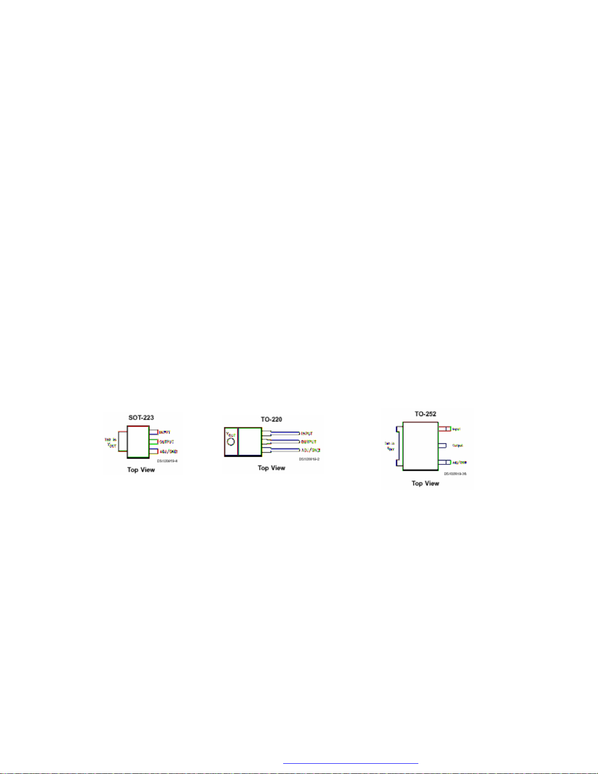
11.11.1. General Description
The LM1117 is a series of low dropout voltage regulators with a dropout of 1.2V at 800mA of load current.
It has the same pin-out as National Semiconductor’s industry standard LM317. The LM1117 is available in
an adjustable version, which can set the output voltage from 1.25V to 13.8V with only two external
resistors. In addition, it is also available in five fixed voltages, 1.8V, 2.5V, 2.85V, 3.3V, and 5V.
The LM1117 offers current limiting and thermal shutdown. Its circuit includes a zener trimmed bandgap
reference to as-sure output voltage accuracy to within ±1%. The LM1117 series is available in SOT-223,
TO-220, and TO-252 D-PAK packages. A minimum of 10µF tantalum capacitor is required at the output to
improve the transient response and stability.
11.11.2. Features
• Available in 1.8V, 2.5V, 2.85V, 3.3V, 5V, and Adjustable Versions
• Space Saving SOT-223 Package
• Current Limiting and Thermal Protection
• Output Current 800mA
• Line Regulation 0.2% (Max)
• Load Regulation 0.4% (Max)
• Temperature Range
— LM1117 0°C to 125°C
— LM1117I -40°C to 125°C
11.11.3. Applications
• 2.85V Model for SCSI-2 Active Termination
• Post Regulator for Switching DC/DC Converter
• High Efficiency Linear Regulators
• Battery Charger
• Battery Powered Instrumentation
11.11.4. Connection Diagrams
15
15
15” TFT TV Service Manual 24/10/2003
PDF created with FinePrint pdfFactory trial version http://www.pdffactory.com
Page 19
11.12. TDA7299
11.12.1. Description
The device TDA7299 is a new technology Mono Audio Amplifier in SO package specially designed for 12V
sound cards application. Thanks to the fully complementary output configuration the device delivers a rail
voltage swing without need of boostrap capacitors.
11.12.2. Features
Can deliver 2W without clipping at 12V/8Ω
Internal fixed gain 20dB
No boucherot cell
Thermal protection
AC short circuit protection
SVR capacitor for better ripple
Rejection
Low turn-on/off pop
Stand-by mode
11.12.3. Pin Connection
16
16
15” TFT TV Service Manual 24/10/2003
PDF created with FinePrint pdfFactory trial version http://www.pdffactory.com
Page 20
11.13. DS90C385
11.13.1. General Description
The DS90C385 transmitter converts 28 bits of LVCMOS/LVTTL data into four LVDS (Low Voltage
Differential Signaling) data streams. A phase-locked transmit clock is transmitted in parallel with the data
streams over a fifth LVDS link.
Every cycle of the transmit clock 28 bits of input data are sampled and transmitted. At a transmit clock
frequency of 85 MHz, 24 bits of RGB data and 3 bits of LCD timing and control data (FPLINE, FPFRAME,
DRDY) are transmitted at a rate of 595 Mbps per LVDS data channel. Using an 85 MHz clock, the data
throughput is 297.5 Mbytes/sec. Also available is the DS90C365 that converts 21 bits of LVCMOS/LVTTL
data into three LVDS (Low Voltage Differential Signaling) data streams. Both transmitters can be
programmed for Rising edge strobe or falling edge strobe through a dedica ted pin. A Rising edge or Falling
edge strobe transmitter will interoperate with a Falling edge strobe Receiver (DS90CF386/DS90CF366)
without any translation logic.
The DS90C385 is also offered in a 64 ball, 0.8mm fine pitch ball grid array (FBGA) package which
provides a 44 % reduction in PCB footprint compared to the TSSOP package. This chipset is an ideal
means to solve EMI and cable size problems associated with wide, high-speed TTL interfaces.
11.13.2. Features
• 20 to 85 MHz shift clock support
• Best–in–Class Set & Hold Times on TxINPUTs
• Tx power consumption <130 mW (typ) @85MHz Grayscale
• Tx Power-down mode <200µW (max)
• Supports VGA, SVGA, XGA and Dual Pixel SXGA.
• Narrow bus reduces cable size and cost
• Up to 2.38 Gbps throughput
• Up to 297.5 Megabytes/sec bandwidth
• 345 mV (typ) swing LVDS devices for low EMI
• PLL requires no external components
• Compatible with TIA/EIA-644 LVDS standard
• Low profile 56-lead or 48-lead TSSOP package
• DS90C385 also available in a 64 ball, 0.8mm fine pitch ball grid array (FBGA) package
11.13.3. Pin Description
DS90C385 MTD56 (TSSOP) Package Pin Description-FPD Link Transmitter
Pin Name I/O No. Description
TxIN
TxOUT+
TxOUT-
TxCLKIN
R_FB
TxCLK OUT+
TxCLK OUT-
PWR DOWN
Vcc
GND
PLL Vcc
PLL GND
LVDS Vcc
LVDS GND
I 28
O 4
O 4
I 1
I 1
O 1
O 1
I 1
I 3
I 4
I 1
I 2
I 1
I 3
TTL level input. This includes: 8 Red, 8 Green, 8 Blue, and 4 control lines —FPLINE,
FPFRAME and DRDY (also referred to as HSYNC, VSYNC, Data Enable).
Positive LVDS differentiaI data output.
Negative LVDS differential data output.
TTL Ievel clock input. Pin name TxCLK IN.
Programmable strobe select
Positive LVDS differential clock output.
Negative LVDS differential clock output.
TTL level input. Assertion (low input) TRI-STATES the outputs, ensuring low current at
power down.
Power supply pins for TTL inputs.
Ground pins for TTL inputs.
Power supply pin for PLL.
Ground pins for PLL.
Power supply pin for LVDS outputs.
Ground pins for LVDS outputs.
17
17
15” TFT TV Service Manual 24/10/2003
PDF created with FinePrint pdfFactory trial version http://www.pdffactory.com
Page 21
DS90C385SLC SLC64A Package Pin Description-FPD Link Transmitter
Pin Name I/O No. Description
TxIN
TxOUT+
TxOUT-
TxCLKIN
R_FB
TxCLK OUT+
TxCLK OUT-
PWR DOWN
Vcc
GND
PLL Vcc
PLL GND
LVDS Vcc
LVDS GND
NC
I 28
O 4
O 4
I 1
I 1
O 1
O 1
I 1
I 3
I 5
I 1
I 2
I 2
I 4
6
TTL level input.
Positive LVDS differentiaI data output.
Negative LVDS differential data output.
TTL Ievel clock input. The rising edge acts as data strobe. Pin name TxCLK IN.
Programmable strobe select. HIGH = rising edge, LOW = falling edge.
Positive LVDS differential clock output.
Negative LVDS differential clock output.
TTL level input. Assertion (low input) TRI-STATES the outputs, ensuring low
current at power down.
Power supply pins for TTL inputs.
Ground pins for TTL inputs.
Power supply pin for PLL.
Ground pins for PLL.
Power supply pin for LVDS outputs.
Ground pins for LVDS outputs.
Pins not connected.
11.14. TDA1308
11.14.1. General Description
The TDA1308 is an integrated class AB stereo headphone driver contained in an SO8 or a DIP8 plastic
package. The device is fabricated in a 1 mm CMOS process and has been primarily developed for portable
digital audio applications.
11.14.2. Features
• Wide temperature range
• No switch ON/OFF clicks
• Excellent power supply ripple rejection
• Low power consumption
• Short-circuit resistant
• High performance
• high signal-to-noise ratio
• High slew rate
• Low distortion
• Large output voltage swing.
11.14.3. Pinning
SYMBOL PIN DESCRIPTION PIN VALUE
OUTA 1 Output A (Voltage swing) Min : 0.75V, Max : 4.25V
INA(neg) 2 Inverting input A Vo(clip) : Min : 1400mVrms
INA(pos) 3 Non-inverting input A 2.5V
VSS 4 Negative supply 0V
INB(pos) 5 Non-inverting input B 2.5V
INB(neg) 6 Inverting input B Vo(clip) : Min : 1400mVrms
OUTB 7 Output B (Voltage swing) Min : 0.75V, Max : 4.25V
VDD 8 Positive supply 5V, Min : 3.0V, Max : 7.0V
18
18
15” TFT TV Service Manual 24/10/2003
PDF created with FinePrint pdfFactory trial version http://www.pdffactory.com
Page 22
11.15. TL431
11.15.1. Description
The TL431 is a 3-terminal adjustable shunt voltage regulator providing a highly accurate 1 % band gap
reference. TL431 acts as an open-loop error amplifier with a 2.5V temperature compensation reference.
The TL431 thermal stability, wide operating current (150mA) and temperature range (0.to 105.makes it
suitable for all variety of application that are looking for a low cost solution with high performance. The
output voltage may be adjusted to any value between VREF and 36 volts with two external resistors. The
TL431 is operating in full industrial temperature range of 0°C to 105°C. The TL431 is available in TO-92,
SO-8, SOT-89 and SOT23-5 packages.
11.15.2. Features
• Trimmed Band gap to 1%
• Wide Operating Current 1mA to 150mA
• Extended Temperature Range 0. °C to 105.°C
• Low Temperature Coefficient 30 ppm /°C
• Offered in TO-92, SOIC, SOT-89, SOT-23-5
• Improved Replacement in Performance for TL431
• Low Cost Solution
11.15.3. Pin Configurations
19
19
15” TFT TV Service Manual 24/10/2003
PDF created with FinePrint pdfFactory trial version http://www.pdffactory.com
Page 23

11.16. 24C16
11.16.1. Description
The AT24C01A/02/04/08/16 provides 1024/2048/4096/8192/16384 bits of serial electrically erasable and
programmable read-only memory (EEPROM) organized as 128/256/512/ 1024/2048 words of 8 bits each.
The device is optimized for use in many industrial and commercial applications where low-power and lowvoltage operation are essential. The AT24C01A/02/04/08/16 is available in space-saving 8-pin PDIP,
(AT24C01A/02/04/08/16), 8-lead TSSOP (AT24C01A/02/04/08/16) and 8-lead JEDEC SOIC (AT24C01A/
02/04/08/16) packages and is accessed via a 2-wire serial interface. In addition, the entire family is
available in 5.0V (4.5V to 5.5V), 2.7V (2.7V to 5.5V), 2.5V (2.5V to 5.5V) and 1.8V (1.8V to 5.5V) versions.
11.16.2. Features
• Low-voltage and Standard-voltage Operation
– 5.0 (V CC = 4.5V to 5.5V)
– 2.7 (V CC = 2.7V to 5.5V)
– 2.5 (V CC = 2.5V to 5.5V)
– 1.8 (V CC = 1.8V to 5.5V)
• Internally Organized 128 x 8 (1K), 256 x 8 (2K), 512 x 8 (4K), 1024 x 8 (8K) or 2048 x 8 (16K)
• 2-wire Serial Interface
• Schmitt Trigger, Filtered Inputs for Noise Suppression
• Bi-directional Data Transfer Protocol
• 100 kHz (1.8V, 2.5V, 2.7V) and 400 kHz (5V) Compatibility
• Write Protect Pin for Hardware Data Protection
• 8-byte Page (1K, 2K), 16-byte Page (4K, 8K, 16K) Write Modes
• Partial Page Writes are Allowed
• Self-timed Write Cycle (10 ms max)
• High-reliability
– Endurance: 1 Million Write Cycles
– Data Retention: 100 Years
• Automotive Grade and Extended Temperature Devices Available
• 8-lead JEDEC SOIC, 8-pin PDIP and 8-lead TSSOP Packages
11.16.3. Pin Configuration
Pin Name Function
A0 - A2 Address Inputs
SDA Serial Data
SCL Serial Clock Input
WP Write Protect
NC No Connect
11.16.4. Pin Description
SERIAL CLOCK (SCL): The SCL input is used to positive edge clock data into each EEPROM device and
negative edge clock data out of each device.
SERIAL DATA (SDA): The SDA pin is bi-directional for serial data transfer. This pin is open-drain driven
and may be wire-ORed with any number of other open-drain or open-collector devices.
DEVICE/PAGE ADDRESSES (A2, A1, A0): The A2, A1 and A0 pins are device address inputs that are
hard wired for the AT24C01A and the AT24C02. As many as eight 1K/2K devices may be addressed on a
single bus system. The AT24C04 uses the A2 and A1 inputs for hard wire addressing and a total of four 4K
devices may be addressed on a single bus system. The A0 pin is a no connect. The AT24C08 only uses
the A2 input for hardwire addressing and a total of two 8K devices may be addressed on a single bus
system. The A0 and A1 pins are no connects. The AT24C16 does not use the device address pins, which
limits the number of devices on a single bus to one. The A0, A1 and A2 pins are no connects.
WRITE PROTECT (WP): The AT24C01A/02/04/16 has a Write Protect pin that provides hardware data
protection. The Write Protect pin allows normal read/write operations when connected to ground (GND).
When the Write Protect pin is connected to VCC, the write protection feature is enabled and operates as
shown in the following table.
20
20
15” TFT TV Service Manual 24/10/2003
PDF created with FinePrint pdfFactory trial version http://www.pdffactory.com
Page 24
11.17. AL875
11.17.1. General Description
The AL875 is a high-speed triple 8-bit monolithic analog-to-digital converter (ADC) designed for digitizing
RGB graphics/video signal or other applications. Its 110 MHz conversion rate can support display
resolution of up to 1280x1024 at 60Hz refresh rate. The AL875 accepts 0.6~2.0V analog input range
without using pre-amplifiers which may reduce the overall S/N ratio. Digitized data is piped at the full clock
rate to the 24-bit output port. The AL875 uses 3.3V power with 5V tolerant I/O and low power dissipation.
The sampling clock is provided by an external clock source, usually a PLL, which multiplies the frequency
of the input reference clock (usually a HSYNC signal) to generate the sampling clock. The AL875 provides
a programmable PLL divider up to 4096. In addition, the input active horizontal and vertical starting and
ending positions can be detected to ensure that the whole picture fits into the displayable region of the
screen. Through an I2C interface, the AL875 is fully programmable to support various graphic resolutions.
11.17.2. General Features
• High speed 8-bit ADC up to 110MHz conversion rate
• Support display resolution up to 1280x1024 at 60Hz refresh rate
• Low power dissipation (0.9W typical at 3.3V, 110MHz)
• 0.6~2.0V p-p analog input range
• 10k~1MHz CKREF locking range
• Full programmability via I2C interface
• Automatic screen position support
• Programmable clock phase adjustment
• TTL compatible digital inputs and outputs
• High impedance tri-state output
• Power-down mode
• Single 3.3 volt power with 5 volt tolerant I/O
• 100-pin 14x20 mm PQFP package
11.17.3. Pin Definition and Description
AL875 Type Pin# Description
TESTIN3 IN (CMOS) 1 Test signal input 3, can be left open.
TESTIN2 IN (CMOS) 2 Test signal input 2, can be left open.
TESTIN1 IN (CMOS) 3 Test signal input 1, can be left open.
TESTIN0 IN (CMOS) 4 Test signal input 0, can be left open.
VDD POWER 5 Digital power supply
VRBR IN 6 Red channel bottom voltage reference
VNR IN 7 Red channel comparator voltage reference
VRTR IN 8 Red channel top voltage reference
NC -- 9 Not connected
NC -- 10 Not connected
VDDAR POWER 11 Red channel analog power supply
RIN IN 12 Red channel analog input
GNDAR GROUND 13 Red channel analog ground
VRBG IN 14 Green channel bottom voltage reference
VNG IN 15 Green channel comparator voltage reference
VRTG IN 16 Green channel top voltage reference
NC -- 17 Not connected
NC -- 18 Not connected
VDDAG POWER 19 Green channel analog power supply
GIN IN 20 Green channel analog input
GNDAG GROUND 21 Green channel analog ground
VRBB IN 22 Blue channel bottom voltage reference
VNB IN 23 Blue channel comparator voltage reference
VRTB IN 24 Blue channel top voltage reference
NC -- 25 Not connected
NC -- 26 Not connected
VDDAB POWER 27 Blue channel analog power supply
BIN IN 28 Blue channel analog input
GNDAB GROUND 29 Blue channel analog ground
ADTEST3 IN (CMOSu) 30 Internal ADC test pin 3, to be pulled up.
CKINTEN IN (CMOSd) 31 Test pin, pulled down for normal operation.
21
21
15” TFT TV Service Manual 24/10/2003
PDF created with FinePrint pdfFactory trial version http://www.pdffactory.com
Page 25

Reserved for AL876 internal clock enable (LO: external clock,
HI: internal PLL clock)
RCLAMP OUT (CMOSt) 32 NC
ADDR1 IN (CMOSd) 33 I2C address control input 1
ADDR2 IN (CMOSd) 34 I2C address control input 2
ADTEST1 IN (CMOSd) 35 Internal ADC test pin 1, to be pulled down.
ADTEST2 IN (CMOSd) 36 Internal ADC test pin 2, to be pulled down.
NC -- 37 Not connected
NC -- 38 Not connected
SDA INOUT (CMOSsu) 39 I2C serial data input/output
VDD POWER 40 Logic digital power supply
GND GROUND 41 Logic digital ground
SCL IN (CMOSs) 42 I2C serial clock input
TESTIN4 IN (CMOSd) 43 Test signal input 4, to be pulled up
/RESET IN (CMOSu) 44 Reset pin (active LOW)
ROF OUT (CMOS) 45 Red channel ADC output overflow
GOF OUT (CMOS) 46 Green channel ADC output overflow
BOF OUT (CMOS) 47 Blue channel ADC output overflow
GNDB GROUND 48 Blue channel ADC output ground
BOUT0 OUT (CMOSt) 49 Blue channel ADC output bit 0
GCLAMP OUT (CMOSt) Not connected
BCLAMP OUT (CMOSt) 51 Not connected
BOUT1 OUT (CMOSt) 52 Blue channel ADC output bit 1
BOUT2 OUT (CMOSt) 53 Blue channel ADC output bit 2
BOUT3 OUT (CMOSt) 54 Blue channel ADC output bit 3
BOUT4 OUT (CMOSt) 55 Blue channel ADC output bit 4
BOUT5 OUT (CMOSt) 56 Blue channel ADC output bit 5
BOUT6 OUT (CMOSt) 57 Blue channel ADC output bit 6
BOUT7 OUT (CMOSt) 58 Blue channel ADC output bit 7
VDDB POWER 59 Blue channel ADC output power supply
GNDG GROUND 60 Green channel ADC output ground
GOUT0 OUT (CMOSt) 61 Green channel ADC output bit 0
GOUT1 OUT (CMOSt) 62 Green channel ADC output bit 1
GOUT2 OUT (CMOSt) 63 Green channel ADC output bit 2
GOUT3 OUT (CMOSt) 64 Green channel ADC output bit 3
GOUT4 OUT (CMOSt) 65 Green channel ADC output bit 4
GOUT5 OUT (CMOSt) 66 Green channel ADC output bit 5
GOUT6 OUT (CMOSt) 67 Green channel ADC output bit 6
GOUT7 OUT (CMOSt) 68 Green channel ADC output bit 7
VDDG POWER 69 Green channel ADC output power supply
GNDR GROUND 70 Red channel ADC output ground
ROUT0 OUT (CMOSt) 71 Red channel ADC output bit 0
ROUT1 OUT (CMOSt) 72 Red channel ADC output bit 1
ROUT2 OUT (CMOSt) 73 Red channel ADC output bit 2
ROUT3 OUT (CMOSt) 74 Red channel ADC output bit 3
ROUT4 OUT (CMOSt) 75 Red channel ADC output bit 4
ROUT5 OUT (CMOSt) 76 Red channel ADC output bit 5
ROUT6 OUT (CMOSt) 77 Red channel ADC output bit 6
ROUT7 OUT (CMOSt) 78 Red channel ADC output bit 7
VDDR POWER 79 Red channel ADC output power supply
CKREFO OUT (CMOS) 80 PLL Reference clock output with phase adjustment from CKREF.
CKAO OUT (CMOS) 81 Output clock A (in phase with the internal digital logic clock)
GNDPLL GROUND 82 Digital ground. Reserved for AL876 PLL digital ground.
CKBO OUT (CMOS) 83 Output clock B (with phase adjustment)
CKADCO OUT (CMOS) 84 ADC sampling clock (in phase with the ADC sampling clock)
VDDPLL POWER 85 Digital power supply. Reserved for AL876 PLL digital power supply.
GND GROUND 86 Digital ground
/OE IN (CMOS) 87 Output enable (when OE is HIGH, the outputs are in HI-Z)
PWRDN IN (CMOSd) 88 Power-Down control (Active HIGH) Clock feedback divider output.
HSFB OUT (CMOS) 89 Used with optional external PLL
HSYNC IN (CMOS) 90 Horizontal sync input
INV IN (CMOSd) 91 The invert control of the ADC sampling clock
CKEXT IN (CMOS) 92 External clock input
Usually used for external PLL reference input.
Suggested to be separated from the other VDD pins with a ferrite bead
for AL876 compatibility
22
22
15” TFT TV Service Manual 24/10/2003
PDF created with FinePrint pdfFactory trial version http://www.pdffactory.com
Page 26

VSYNC IN (CMOS) 93 Vertical sync input
CKREF IN (CMOS) 94 PLL reference clock input
VDD POWER 95 Digital power supply
GNDAPLL GROUND 96 Analog ground. Reserved for AL876 PLL analog ground.
CP IN 97 Internal compensation pin. Reserved for AL876 PLL filter input. Please
NC -- 98 Not connected
VDDAPLL POWER 99 Analog power supply. Reserved for AL876 PLL analog power supply.
GND GROUND 100 Digital ground
follow the reference design for external RC filter circuitry.
Suggested to be separated from the other VDD pins with a ferrite bead
for AL876 compatibility
11.18. 74HC244A
11.18.1. Description
The 74HC244 is an advanced high-speed CMOS OCTAL BUS BUFFER (3-STATE) fabricated with silicon
gate C2MOS technology. G control input governs four BUS BUFFERs. This device is designed to be used
with 3 state memory address drivers, etc. All inputs are equipped with protection circuits against static
discharge and transient excess voltage.
11.18.2. General Features
• High speed: t PD = 10ns (typ.) at VCC =6V
• Low power dissipation: ICC =4μA (max) at TA =25°C
• High noise immunity: VNIH =VNIL =28%VCC (min.)
• Symmetrical output impedance: |IOH |=IOL = 6mA (min)
• Balanced propagation delays: tPLH ≅ tPHL
• Wide operating voltage range: VCC(Opr) = 2V to 6V
• Pin and function compatible with 74 series 244
11.18.3. Pin Description
Pin no Symbol Name and function
1 1G Output Enable Input
2, 4, 6, 8 1A1 to 1A4 Data Inputs
9, 7, 5, 3 2Y1 to 2Y4 Data Outputs
11, 13, 15, 17 2A1 to 2A4 Data Inputs
18, 16, 14, 12 1Y1 to 1Y4 Data Outputs
19 2G Output Enable Input
10 GND Ground (0V)
20 VCC Positive Supply Voltage
23
23
15” TFT TV Service Manual 24/10/2003
PDF created with FinePrint pdfFactory trial version http://www.pdffactory.com
Page 27

11.19. ICS1523
11.19.1. Description
The ICS 1523 is a low-cost but very high-performance frequency generator for line-locked and genlocked
high-resolution video applications. Using ICS ’s advanced low-voltage CMOS mixed-mode technology, the
ICS 1523 is an effective clock solution for video projectors and displays at resolutions from VGA to beyond
UXGA. The ICS 1523 offers pixel clock outputs in both differential (to 250 MHz) and single-ended (to 150
MHz) formats. Dynamic Phase Adjust™ circuitry allows user control of the pixel clock phase relative to the
recovered sync signal. A second differential output at half the pixel clock rate enables deMUXing of
multiplexed analog-to-digital converters. The FUNC pin provides either the regenerated input from the
phase-locked loop (PLL) divider chain output or a re-synchronized and sharpened input HSYNC. The
advanced PLL uses either its internal programmable feedback divider or an external divider. The device is
programmed by a standard I2C-bus™ serial interface and is available in a 24-pin small-outline integrated
circuit (SOIC) package.
11.19.2. Features
• Pixel clock frequencies up to 250 MHz
• Very low jitter
• Dynamic Phase Adjust (DPA) for clock outputs
• Balanced PECL differential outputs
• Single-ended SSTL_3 clock outputs
• Double-buffered PLL/DPA control registers
• Independent software reset for PLL/DPA
• External or internal loop filter selection
• Uses 3.3 Vdc. Inputs are 5 V-tolerant.
• I2C-bus™ serial interface can run at either low speed (100 kHz) or high speed (400 kHz).
• Lock detection
• 24-pin 300-mil SOIC package
24
24
15” TFT TV Service Manual 24/10/2003
PDF created with FinePrint pdfFactory trial version http://www.pdffactory.com
Page 28

11.20. MC34063
11.20.1. Description
The MC34063A Series is a monolithic control circuit containing the primary functions required for DC–to–
DC converters. These devices consist of an internal temperature compensated reference, comparator,
controlled duty cycle oscillator with an active current limit circuit, driver and high current output switch. This
series was specifically designed to be incorporated in Step–Down and Step–Up and Voltage–Inverting
applications with a minimum number of external components.
11.20.2. Features
• Operation from 3.0 V to 40 V Input
• Low Standby Current
• Current Limiting
• Output Switch Current to 1.5 A
• Output Voltage Adjustable
• Frequency Operation to 100 kHz
• Precision 2% Reference
11.20.3. Pin connections
25
25
15” TFT TV Service Manual 24/10/2003
PDF created with FinePrint pdfFactory trial version http://www.pdffactory.com
Page 29

11.21. TDA9885/86
11.21.1. General description
The TDA9885 is an alignment-free single standard (without positive modulation) vision and sound IF signal PLL.
The TDA9886 is an alignment-free multistandard (PAL, SECAM and NTSC) vision and sound IF signal PLL
demodulator for positive and negative modulation including sound AM and FM processing.
Both devices can be used for TV, VTR, PC and set-top box applications.
11.21.2. 13.13.2.Features
• 5 V supply voltage
• Gain controlled wide-band Vision Intermediate Frequency (VIF) amplifier (AC-coupled)
• Multistandard true synchronous demodulation with active carrier regeneration (very linear demodulation, good
intermodulation figures, reduced harmonics, excellent pulse response)
• Gated phase detector for L/L accent standard
• Fully integrated VIF Voltage Controlled Oscillator (VCO), alignment-free; frequencies switchable for all
negative and positive modulated standards via I2C-bus
• Digital acquisition help, VIF frequencies of 33.4, 33.9, 38.0, 38.9, 45.75 and 58.75 MHz
• 4 MHz reference frequency input [signal from Phase-Locked Loop (PLL) tuning system] or operating as crystal
oscillator
• VIF Automatic Gain Control (AGC) detector for gain control, operating as peak sync detector for negative
modulated signals and as a peak white detector for positive modulated signals
• Precise fully digital Automatic Frequency Control (AFC) detector with 4-bit digital-to-analog converter; AFC bits
via I2C -bus readable
• TakeOver Point (TOP) adjustable via I2C-bus or alternatively with potentiometer
• Fully integrated sound carrier trap for 4.5, 5.5, 6.0 and 6.5 MHz, controlled by FM-PLL oscillator
• Sound IF (SIF) input for single reference Quasi Split Sound (QSS) mode (PLL controlled)
• SIF AGC for gain controlled SIF amplifier; single reference QSS mixer able to operate in high
performance single reference QSS mode and in intercarrier mode, switchable via I2C-bus
• AM demodulator without extra reference circuit
• Alignment-free selective FM-PLL demodulator with high linearity and low noise
• I2C-bus control for all functions
• I2C-bus transceiver with pin programmable Module Address (MAD).
11.21.3. 13.13.3.Pinning
SYMBOL PIN DESCRIPTION
VIF1 1 VIF differential input 1
VIF2 2 VIF differential input 2
OP1 3 output 1 (open-collector)
FMPLL 4 FM-PLL for loop filter
DEEM 5 de-emphasis output for capacitor
AFD 6 AF decoupling input for capacitor
DGND 7 digital ground
AUD 8 audio output
TOP 9 tuner AGC TakeOver Point (TOP)
SDA 10 I2C-bus data input/output
SCL 11 I2C-bus clock input
SIOMA 12 sound intercarrier output and MAD select
n.c. 13 not connected
TAGC 14 tuner AGC output
REF 15 4 MHz crystal or reference input
VAGC 16 VIF-AGC for capacitor (Not connected for TDA9885)
CVBS 17 video output
AGND 18 analog ground
VPLL 19 VIF-PLL for loop filter
VP 20 supply voltage (+5 V)
AFC 21 AFC output
OP2 22 output 2 (open-collector)
SIF1 23 SIF differential input 1
SIF2 24 SIF differential input 2
26
26
15” TFT TV Service Manual 24/10/2003
PDF created with FinePrint pdfFactory trial version http://www.pdffactory.com
Page 30

11.22. MSP34X0G
MSP3400G
Multistandard Sound Processor Family
11.22.1. Introduction
The MSP 34x0G family of single-chip Multistandard Sound Processors covers the sound processing of all
analog TV-Standards worldwide, as well as the NICAM digital sound standards. The full TV sound
processing, starting with analog sound IF signal-in, down to processed analog AF-out, is performed on a
single chip. Figure shows a simplified functional block diagram of the MSP 34x0G.
This new generation of TV sound processing ICs now includes versions for processing the multichannel
television sound (MTS) signal conforming to the standard recommended by the Broadcast Television
Systems Committee (BTSC). The DBX noise reduction, or alternatively, MICRONAS Noise Reduction
(MNR) is performed alignment free. Other processed standards are the Japanese FM-FM multiplex
standard (EIA-J) and the FM Stereo Radio standard. Current ICs have to perform adjustment procedures
in order to achieve good stereo separation for BTSC and EIA-J. The MSP 34x0G has optimum stereo
performance without any adjustments.
All MSP 34x0G versions are pin and software downward compatible to the MSP 34x0D. The MSP 34x0G
further simplifies controlling software. Standard selection
requires a single I²C transmission only.
The MSP 34x0G has built-in automatic functions: The IC is able to detect the actual sound standard
automatically (Automatic Standard Detection). Furthermore, pilot levels and identification signals can be
evaluated internally with subsequent switching between mono/stereo/bilingual; no I²C interaction is
necessary (Automatic Sound Selection).
Source Select
I2S bus interface consists of five pins:
1. I2S_DA_IN1, I2S_DA_IN2: For input, four channels (two channels per line, 2*16 bits) per sampling cycle
(32 kHz) are transmitted.
2. I2S_DA_OUT: For output, two channels (2*16 bits) per sampling cycle (32 kHz) are transmitted.
3. I2S_CL: Gives the timing for the transmission of I2S serial data (1.024 MHz).
4. I2S_WS: The I2S_WS word strobe line defines the left and right sample.
11.22.2. Features
• Standard Selection with single I2C transmission
• Automatic Standard Detection of terrestrial TV standards
• Automatic Sound Selection (mono/stereo/bilingual), new registers MODUS, STATUS
• Two selectable sound IF (SIF) inputs
• Automatic Carrier Mute function
• Interrupt output programmable (indicating status change)
• Loudspeaker / Headphone channel with volume, balance, bass, treble, loudness
• AVC: Automatic Volume Correction
27
27
15” TFT TV Service Manual 24/10/2003
PDF created with FinePrint pdfFactory trial version http://www.pdffactory.com
Page 31

• Subwoofer output with programmable low-pass and complementary high-pass filter
• 5-band graphic equalizer for loudspeaker channel
• Spatial effect for loudspeaker channel
• Four Stereo SCART (line) inputs, one Mono input; two Stereo SCART outputs
• Complete SCART in/out switching matrix
• Two I2S inputs; one I2S output
• Dolby Pro Logic with DPL 351xA coprocessor
• All analog FM-Stereo A2 and satellite standards; AM-SECAM L standard
• Simultaneous demodulation of (very) high-deviation FM-Mono and NICAM
• Adaptive deemphasis for satellite (Wegener-Panda, acc. to ASTRA specification)
• ASTRA Digital Radio (ADR) together with DRP 3510A
• All NICAM standards
• Korean FM-Stereo A2 standard
11.22.3. Pin connections
NC = not connected; leave vacant
LV = if not used, leave vacant
OBL = obligatory; connect as described in circuit diagram
DVSS: if not used, connect to DVSS
AHVSS: connect to AHVSS
Pin No. Pin Name Type
PLCC
68-pin
1 16 14 9 8 ADR_WS OUT LV ADR word strobe
2 - - - - NC LV Not connected
3 15 13 8 7 ADR_DA OUT LV ADR Data Output
4 14 12 7 6 I2S_DA_IN1 IN LV I2S1 data input
5 13 11 6 5 I2S_DA_OUT OUT LV I2S data output
6 12 10 5 4 I2S_WS IN/OUT LV I2S word strobe
7 11 9 4 3 I2S_CL IN/OUT LV I2S clock
8 10 8 3 2 I2C_DA IN/OUT OBL I2C data
9 9 7 2 1 I2C_CL IN/OUT OBL I2C clock
10 8 - 1 64 NC LV Not connected
11 7 6 80 63 STANDBYQ IN OBL Stand-by (low-active)
12 6 5 79 62 ADR_SEL IN OBL I2C bus address select
13 5 4 78 61 D_CTR_I/O_0 IN/OUT LV D_CTR_I/O_0
14 4 3 77 60 D_CTR_I/O_1 IN/OUT LV D_CTR_I/O_1
15 3 - 76 59 NC LV Not connected
16 2 - 75 58 NC LV Not connected
17 - - - - NC LV Not connected
18 1 2 74 57 AUD_CL_OUT OUT LV
19 64 1 73 56 TP LV Test pin
20 63 52 72 55 XTAL_OUT OUT OBL Crystal oscillator
21 62 51 71 54 XTAL_IN IN OBL Crystal oscillator
22 61 50 70 53 TESTEN IN OBL Test pin
23 60 49 69 52 ANA_IN2+ IN
24 59 48 68 51 ANA_IN- IN
25 58 47 67 50 ANA_IN1+ IN LV IF input 1
26 57 46 66 49 AVSUP OBL Analog power supply 5V
- - - 65 - AVSUP OBL Analog power supply 5V
- - - 64 - NC LV Not connected
- - - 63 - NC LV Not connected
27 56 45 62 48 AVSS OBL Analog ground
- - - 61 - AVSS OBL Analog ground
28 55 44 60 47 MONO_IN IN LV Mono input
- - - 59 - NC LV Not connected
29 54 43 58 46 VREFTOP OBL
30 53 42 57 45 SC1_IN_R IN LV SCART 1 input, right
31 52 41 56 44 SC1_IN_L IN LV SCART 1 input, left
32 51 - 55 43 ASG1 AHVSS Analog Shield Ground 1
33 50 40 54 42 SC2_IN_R IN LV SCART 2 input, right
PSDIP
64-pin
PSDIP
52-pin
PQFP
80-pin
PLQFP
64-pin
Connection
(if not used)
AVSS via
56 pF/LV
AVSS via
56 pF/LV
Short Description
Audio clock output
(18.432 MHz)
IF Input 2 (can be left
vacant, only if IF input 1 is
also not in use)
IF common (can be left
vacant, only if IF input 1 is
also not in use)
Reference voltage IF A/D
converter
28
28
15” TFT TV Service Manual 24/10/2003
PDF created with FinePrint pdfFactory trial version http://www.pdffactory.com
Page 32

34 49 39 53 41 SC2_IN_L IN LV SCART 2 input, left
35 48 - 52 40 ASG2 AHVSS Analog Shield Ground 2
36 47 38 51 39 SC3_IN_R IN LV SCART 3 input, right
37 46 37 50 38 SC3_IN_L IN LV SCART 3 input, left
38 45 - 49 37 ASG4 AHVSS Analog Shield Ground 4
39 44 - 48 36 SC4_IN_R IN LV SCART 4 input, right
40 43 - 47 35 SC4_IN_L IN LV SCART 4 input, left
41 - - 46 - NC LV or AHVSS Not connected
42 42 36 45 34 AGNDC OBL Analog reference voltage
43 41 35 44 33 AHVSS OBL Analog ground
- - - 43 - AHVSS OBL Analog ground
- - - 42 - NC LV Not connected
- - - 41 - NC LV Not connected
44 40 34 40 32 CAPL_M OBL Volume capacitor MAIN
45 39 33 39 31 AHVSUP OBL Analog power supply 8V
46 38 32 38 30 CAPL_A OBL Volume capacitor AUX
47 37 31 37 29 SC1_OUT_L OUT LV SCART output 1, left
48 36 30 36 28 SC1_OUT_R OUT LV SCART output 1, right
49 35 29 35 27 VREF1 OBL Reference ground 1
50 34 28 34 26 SC2_OUT_L OUT LV SCART output 2, left
51 33 27 33 25 SC2_OUT_R OUT LV SCART output 2, right
52 - - 32 - NC LV Not connected
53 32 - 31 24 NC LV Not connected
54 31 26 30 23 DACM_SUB OUT LV Subwoofer output
55 30 - 29 22 NC LV Not connected
56 29 25 28 21 DACM_L OUT LV Loudspeaker out, left
57 28 24 27 20 DACM_R OUT LV Loudspeaker out, right
58 27 23 26 19 VREF2 OBL Reference ground 2
59 26 22 25 18 DACA_L OUT LV Headphone out, left
60 25 21 24 17 DACA_R OUT LV Headphone out, right
- - - 23 - NC LV Not connected
- - - 22 - NC LV Not connected
61 24 20 21 16 RESETQ IN OBL Power-on-reset
62 23 - 20 15 NC LV Not connected
63 22 - 19 14 NC LV Not connected
64 21 19 18 13 NC LV Not connected
65 20 18 17 12 I2S_DA_IN2 IN LV I2S2-data input
66 19 17 16 11 DVSS OBL Digital ground
- - - 15 - DVSS OBL Digital ground
- - - 14 - DVSS OBL Digital ground
67 18 16 13 10 DVSUP OBL Digital power supply 5V
- - - 12 - DVSUP OBL Digital power supply 5V
- - - 11 - DVSUP OBL Digital power supply 5V
68 17 15 10 9 ADR_CL OUT LV ADR clock
29
29
15” TFT TV Service Manual 24/10/2003
PDF created with FinePrint pdfFactory trial version http://www.pdffactory.com
Page 33

11.23. SAA3010T
11.23.1. 14.22.1.Description
The SAA3010 is intended as a general purpose (RC-5) infrared remote control system for use where a low
voltage supply and a large debounce time are expected. The device can generate 2048 different commands and
utilizes a keyboard with a single pole switch for each key. The commands are arranged so that 32 systems can
be addressed, each system containing 64 different commands. The circuit response to legal (one key pressed at
a time) and illegal (more than one key pressed at a time) keyboard operation is specified in the section
“Keyboard operation”.
11.23.2. 14.22.2.Features
Low voltage requirement
Biphase transmission technique
Single pin oscillator
Test mode facility
11.23.3. 14.22.3.Pinning
Pin Mnemonic Function
1 X7 (IPU) sense input from key matrix
2 SSM (I) sense mode selection input
3 Z0-Z3 (IPU) sense inputs from key matrix
7 MDATA (OP3) generated output data modulated with 1/12 the oscillator frequency at a 25% duty factor
8 DATA (OP3) generated output information
9-13 DR7-DR3 (ODN) Scan drivers
14 VSS Ground (0V)
15-17 DR-2-DR0 (ODN) Scan drivers
18 OSC (I) Oscillator input
19 TP2 (I) test point 2
20 TP1 (I) Test point 1
21-27 X0-X6 (IPU) Sense inputs from key matrix
28 VDD(I) Voltage supply
Note:
(I): Input,
(IPU): input with p-channel pull-up transistor,
(ODN): output with open drain n-channel transistor
(OD3): output 3-state
30
30
15” TFT TV Service Manual 24/10/2003
PDF created with FinePrint pdfFactory trial version http://www.pdffactory.com
Page 34

12. SERVICE MENU SETTINGS
All system, geometry and white balance alignments are performed in production service mode. Before
starting the production mode alignments, make sure that all manual adjustments are done correctly. To
start production mode alignments enter the MAIN MENU and then press the digits 4, 7, 2 and 5
respectively. The following menu appears on the screen.
LCDTFT33 4.0.12.
After entering the Service menu, you can access its items by pressing “P+/P-“ buttons. In order to enter
selected menu, use “VOL+/VOL-“ buttons. To exit the service menu press “MENU” button.
Entire service menu parameters of TFT TV are listed below.
In order to enter Adjust menu, move the cursor to Adjust… parameter by pressing “P+/P-“ buttons in
Service Menu and press “VOL+/VOL-“ button. The following menu appears on the screen.
0028
There are 14 items in the ADJUST menu, but 10 of them are seen when you first enter the menu. Using
VOL+/VOL- buttons remaining items can be seen.
Horiz . Position: Horizontal Position
Adjusts the horizontal positon of the screen.
Min. Value: 0000
Max. Value: 0063
Recommended Value: 0009
Vert . Position: Vertical Position
Adjusts the vertical positon of the screen.
Min. Value: 0020
Max. Value: 0242
Recommended Value: 0167
Active Width
Adjusts the width of the screen.
Min. Value: 0000
Max. Value: 0063
Recommended Value: 0063
Service
Adjust...
Options...
Aps Wss Test
12.1. ADJUST MENU SETTINGS
Adjust...
Horiz. Position
Vert. Position
Active Width
Active Height
Horiz. Total
Horiz. Border
Vert. Border
Hsync Phase
Auto Position
Resolution
31
31
15” TFT TV Service Manual 24/10/2003
PDF created with FinePrint pdfFactory trial version http://www.pdffactory.com
Page 35

Active Height
Adjusts the height of the screen.
Min. Value: 0000
Max. Value: 0063
Recommended Value: 0063
Horiz . Total: Horizontal Total
Min. Value: 0000
Max. Value: 0063
Recommended Value: 0028
Horiz . Border: Horizontal Border
Adjusts the thickness of the horizontal border.
Min. Value: 0000
Max. Value: 0255
Recommended Value: 0000
Vert . Border: Vertical Border
Adjusts the thickness of the vertical border.
Min. Value: 0000
Max. Value: 0255
Recommended Value: 0000
Hsync Phase
Min. Value: 0000
Max. Value: 0015
Recommended Value: 0000
Auto Position Resolution
Value: 1024*0236
Total
Value: 1142*0262
Adjust...
Horiz. Total
Horiz. Border
Vert. Border
Hsync Phase
Auto Position
Resolution
Total
V Freq
Reset
Store
0028
V Freq
Value: 0060
Reset
Resets the adjust menu values.
Store
Stores the entered adjust menu values.
32
32
15” TFT TV Service Manual 24/10/2003
PDF created with FinePrint pdfFactory trial version http://www.pdffactory.com
Page 36

OPTIONS MENU SETTINGS
In order to enter Options menu, move the cursor to Options… parameter by pressing “P+/P-“ buttons in
Service Menu and press “VOL+/VOL-“ button. The following menu appears on the screen.
000: On
There are 50 items in the OPTIONS menu, but 10 of them are seen when you first enter the menu. Using
P+/P- buttons remaining items can be seen.
Hue On/Off
Set ON
First APS On/Off
If ON, TV starts with APS menu at Start-up. Set OFF
A.P.S On/Off
enable/disable Automatic Programming System. Set ON
Headphone On/Off
enable/disable the usage of the HP and HP related items in sound menu. Set ON
Options...
Hue
First APS
A.P.S.
Headphone
Vsr
DBE
Subwoofer
Lineout
Dolby prologic
Equalizer
Vsr On/Off
enable/disable Vsr. Set OFF
DBE On/Off
enable/disable DBE. Set OFF
Subwoofer On/Off
enable/disable Subwoofer. Set OFF
Lineout On/Off
enable/disable Lineout. Set ON
Dolby prologic On/Off
enable/disable dolby prologic system. Set OFF
Equalizer On/Off
enable/disable equalizer system. Set ON
BG On/Off
enable/disable BG Standard. Set ON
DK On/Off
enable/disable DK Standard. Set OFF
33
33
15” TFT TV Service Manual 24/10/2003
PDF created with FinePrint pdfFactory trial version http://www.pdffactory.com
Page 37

Options...
Equalizer
BG
DK
I
L
L’
M
N
NM
FM Prs Avl On
009: On
I On/Off
enable/disable I Standard. Set OFF
L/L’ On/Off
enable/disable L/L’ Standard. Set OFF
M On/Off
enable/disable M Standard. Set OFF
N On/Off
enable/disable N Standard. Set OFF
NM On/Off
enable/disable M Standard. Set OFF
FM Prs Avl On
Adjusts the FM Prescaler value, when Automatic Volume Levelling is On
Min. Value: 0000 00000
Max. Value: 00FF 00255
Recommended Value: 000F 00015: for 4 ohm
Recommended Value: 0011 00017: for 8 ohm
Options...
FM Prs Avl On
Nicam Prs Avl On
Scart Prs Avl On
Scart Volume Avl On
FM Prs Avl Off
Nicam Prs Avl Off
Scart Prs Avl Off
Scart Volume Avl Off
Equ Coe.0
Equ Coe.1
018: 000F 00015
34
34
15” TFT TV Service Manual 24/10/2003
PDF created with FinePrint pdfFactory trial version http://www.pdffactory.com
Page 38

Nicam Prs Avl On
Adjusts the Nicam Prescaler value, when Automatic Volume Levelling is On
Min. Value: 0000 00000
Max. Value: 00FF 00255
Recommended Value: 0022 00034: for 4 ohm
Recommended Value: 0028 00040: for 8 ohm
Scart Prs Avl On
Adjusts the Scart Prescaler value, when Automatic Volume Levelling is On
Min. Value: 0000 00000
Max. Value: 00FF 00255
Recommended Value: 000F 00015: for 4 ohm
Recommended Value: 0010 00016: for 8 ohm
Scart Volume Avl On
Adjusts the Scart Volume value, when Automatic Volume Levelling is On
Min. Value: 0000 00000
Max. Value: 00FF 00255
Recommended Value: 0035 00053: for 4 ohm
Recommended Value: 0035 00053: for 8 ohm
FM Prs Avl Off
Adjusts the FM Prescaler value, when Automatic Volume Levelling is Off
Min. Value: 0000 00000
Max. Value: 00FF 00255
Recommended Value: 0008 00008: for 4 ohm
Recommended Value: 000A 00010: for 8 ohm
Nicam Prs Avl Off
Adjusts the Nicam Prescaler value, when Automatic Volume Levelling is Off
Min. Value: 0000 00000
Max. Value: 00FF 00255
Recommended Value: 0013 00019: for 4 ohm
Recommended Value: 0017 00023: for 8 ohm
Scart Prs Avl Off
Adjusts the Scart Prescaler value, when Automatic Volume Levelling is Off
Min. Value: 0000 00000
Max. Value: 00FF 00255
Recommended Value: 0008 00008: for 4 ohm
Recommended Value: 0009 00009: for 8 ohm
Scart Volume Avl Off
Adjusts the Scart Volume value, when Automatic Volume Levelling is Off
Min. Value: 0000 00000
Max. Value: 00FF 00255
Recommended Value: 0035 00053: for 4 ohm
Recommended Value: 0035 00053: for 8 ohm
Equ Coe.0
Min. Value: 0000 00000
Max. Value: FFFF 65535
Recommended Value: FFFF 65535
Equ Coe.1
Min. Value: 0000 00000
Max. Value: FFFF 65535
Recommended Value: FFFF 65535
35
35
15” TFT TV Service Manual 24/10/2003
PDF created with FinePrint pdfFactory trial version http://www.pdffactory.com
Page 39

Options...
Equ Coe.1
Equ Coe.2
Equ Coe.3
Avl
Top TXT
Fast TXT
TXT Lang
IF Freq
Sound
Carrier
027: FFFF 65535
Equ Coe.2
Min. Value: 0000 00000
Max. Value: FFFF 65535
Recommended Value: FFFF 65535
Equ Coe.3
Min. Value: 0000 00000
Max. Value: FFFF 65535
Recommended Value: FFFF 65535
Avl On/Off
enable/disable Automatic Volume Levelling System. Set ON
Top TXT On/Off
enable/disable Top TXT. Set OFF
Fast TXT On/Off
enable/disable Fast TXT. Set ON
TXT Lang
Switches between Teletext Language Groups
Min. Value: 0000 00000
Max. Value: 0004 00004
Recommended Value: 0000 00000
IF Freq
Adjusts the IF Frequency
Min. Value: 0000 00000
Max. Value: 00FF 00255
Recommended Value: 0000 00000
Sound On/Off
enable/disable Sound. Set ON
Carrier On/Off
enable/disable Carrier. Set ON
RC_1541 On/Off
Enables/disables Remote control usage for Service menu. Set ON.
AV-1 On/Off
enable/disable AV-1. Set ON
36
36
15” TFT TV Service Manual 24/10/2003
PDF created with FinePrint pdfFactory trial version http://www.pdffactory.com
Page 40

Options...
Carrier
RC_1541
AV-1
AV-2
PC
S-VHS
RGB
MENU
CB
BV1
036: On
AV-2 On/Off
enable/disable AV-2. Set ON
PC On/Off
enable/disable PC. Set ON
S-VHS On/Off
enable/disable S-VHS. Set ON
RGB On/Off
enable/disable RGB. Set ON
Options...
S-VHS
RGB
MENU
CB
BV1
BV3
BU
V1-V3
V3_U
AGC
050: FFFF 65535
MENU On/Off
enable/disable semi-transparent MENU. Set OFF.
CB
Min. Value: 00000000
Max. Value: 11111111
Recommended Value: 00001101
BV1
Min. Value: 00000000
Max. Value: 11111111
Recommended Value: 00001101
37
37
15” TFT TV Service Manual 24/10/2003
PDF created with FinePrint pdfFactory trial version http://www.pdffactory.com
Page 41

BV3
Min. Value: 00000000
Max. Value: 11111111
Recommended Value: 00001101
BU
Min. Value: 00000000
Max. Value: 11111111
Recommended Value: 00001101
V1-V3
Min. Value: 0000 00000
Max. Value: FFFF 65535
Recommended Value: 0D0D 03341
V3_U
Min. Value: 0000 00000
Max. Value: FFFF 65535
Recommended Value: 0D0D 03341
AGC
Adjusts the Automatic Gain Control value.
Min. Value: 0000 00000
Max. Value: 001F 00031
Recommended Value: 000A 00010
12.2. APS WSS TEST MENU
In order to enter Aps Wss Test menu, move the cursor to Aps Wss Test parameter by pressing P+/Pbuttons in Service Menu and press VOL+/VOL- button. The following menu appears on the screen.
Aps Wss Test
Programme
Search
VPS
Pdc Format 1
Pdc Format 2
Name
Wss
P 08
CNN S 04 BG 463
There are 7 items in the Aps Wss Test menu.
Programme
Search
VPS
Pdc Format 1
Pdc Format 2
Name
Wss
38
38
15” TFT TV Service Manual 24/10/2003
PDF created with FinePrint pdfFactory trial version http://www.pdffactory.com
Page 42

13. BLOCK DIAGRAM
Tuner
UV1316
Philips
IF IC
TDA988X
Philips
Text RGB, FB
Video Output
CVBS_IF
CVBS_scart
CVBS_FAV
S-Video
RGB, FB
Scart_Audio_In
AV_Audio In
Audio_Out
VPC 3230
Video Pro.
Micronas
QSS
Audio Processor
16-bit YUV 4:2:2
24-bit RGB
4:4:4
MSP3410G
Micronas
Audio_L
Audio_R
AL 300
LCD Cont.
Averlogic
TDA7299
Audio Amp.
ST
TDA7299
Audio Amp.
ST
3x8 bit RGB
90C385
LVDS Tx
National
LVDS
15”TFT
PANEL
Text RGB, FB
Selected
Video
AL 875
Triple ADC
Averlogic
SDA5555
MCU
Micronas
15” TFT TV Service Manual 24/10/2003
I2C
RGB,
Hsync
Vsync
Graphics RGB
VGA
PDF created with FinePrint pdfFactory trial version http://www.pdffactory.com
39
39
PLL IC
ICS 1523
ICS
SDA
SCL
DDC IC
24LC21
ST
PC Graphics Option
Page 43

14. CIRCUIT DIAGRAMS
17MB01P-1
001
15” TFT TV Service Manual 24/10/2003
PDF created with FinePrint pdfFactory trial version http://www.pdffactory.com
40
40
Page 44

17MB01P-1
002
15” TFT TV Service Manual 24/10/2003
PDF created with FinePrint pdfFactory trial version http://www.pdffactory.com
41
41
Page 45

17MB01P-1
003
15” TFT TV Service Manual 24/10/2003
PDF created with FinePrint pdfFactory trial version http://www.pdffactory.com
42
42
Page 46

17MB01P-1
004
15” TFT TV Service Manual 24/10/2003
PDF created with FinePrint pdfFactory trial version http://www.pdffactory.com
43
43
Page 47

17MB01P-1
005
15” TFT TV Service Manual 24/10/2003
PDF created with FinePrint pdfFactory trial version http://www.pdffactory.com
44
44
Page 48

17MB01P-1
006
15” TFT TV Service Manual 24/10/2003
PDF created with FinePrint pdfFactory trial version http://www.pdffactory.com
45
45
Page 49

17MB01P-1
007
15” TFT TV Service Manual 24/10/2003
PDF created with FinePrint pdfFactory trial version http://www.pdffactory.com
46
46
Page 50

17MB01P-1
008
15” TFT TV Service Manual 24/10/2003
PDF created with FinePrint pdfFactory trial version http://www.pdffactory.com
47
47
Page 51

17TK01
15” TFT TV Service Manual 24/10/2003
PDF created with FinePrint pdfFactory trial version http://www.pdffactory.com
48
48
Page 52

17PLL01-4
15” TFT TV Service Manual 24/10/2003
PDF created with FinePrint pdfFactory trial version http://www.pdffactory.com
49
49
Page 53

1LD01-2
50
50
15” TFT TV Service Manual 24/10/2003
PDF created with FinePrint pdfFactory trial version http://www.pdffactory.com
Page 54

11UK10-2
51
15” TFT TV Service Manual
24/10/2003
PDF created with FinePrint pdfFactory trial version http://www.pdffactory.com
Page 55

Page 56

Page 57

Page 58

Page 59

Page 60

Page 61

Page 62

Page 63

Page 64

Page 65

Page 66

Page 67

Product Code Description
10023111 17MB01 TFT 1506 VE.IBE.SANYO CE15L06(SLV
Serial No Component Code Comp. Descrip.
2004.04.04 0043147673
Component Code Description Position Number
5580117 20139810 CHS.ASSY.17MB01-11111112131111
5586818 20139810 CHS.ASSY.17MB01-11111112131111
ELECTRONICS
20101428 MD.ASY.17PLL01-PLL TUNER (TFT/17MB01)
20103886 SPK.AS.1500/4/5/6 8R*3,5 TFT (R/L)
20122348 PR.IC.17MB01P-TFT OSD
20123319 IC 24C16 TFT010192112110011
20134451 MD.ASY.17LD01A-LED KARTI 1506 TFT
20134483 MD.ASY.17TK01P-W/ON-OFF 1504/5/6/7/8(5SW
20139810 CHS.ASSY.17MB01-111111121311111
30000068 CAP MKT 1NF 63V K ROHS
30000074 CAP MKT 100NF 63V J RoHS
30000109 CAP MKT 470NF 63V J ROHS
30000257 CAP CER 470PF 50V J SL ROHS
30000294 CAP SMD 100NF 50V K (0805) ROHS
. .
. . . . .
. . . . .
. . . . .
. . . . .
. . . . .
. . . . .
. . . . .
C112 . . . .
C475 C476 . . .
C113 C115 C608 C114 C140
CXX2 . . . .
C60 C62 . . .
C767 . . . .
. .
30000315 CAP SMD 220NF 25V Z (0805) ROHS
. .
. .
. .
30000345 CAP EL 10UF 50V M
. .
. .
. .
30000352 CAP EL 100UF 16V M ROHS
. .
C819 C121 C122 C123 .
C439 C440 . . .
C107 C128 C414 C415 C416
C417 C134 C135 C136 C150
C753 C757 C756 C775 C776
C110 C116 C421 C422 C423
C480 C623 C817 C825 C157
C768 . . . .
C218 C221 C222 . .
C443 C445 . . .
C402 C611 C809 C820 C147
Page 68

. .
C522 C627 C823 C483 .
30000359 CAP EL 1000UF 16V M. ROHS
30000362 CAP EL 1UF 50V M. ROHS
. .
30000371 CAP EL 22UF 50V M ROHS
. .
. .
30000393 CAP EL 3.3UF 50V M ROHS
30000395 CAP EL 47UF 6.3V M (4*7MM) ROHS
30000400 CAP EL 47UF 50V M
. .
30000407 CAP EL 470UF 16V M. ROHS
30000413 CAP EL 4.7UF 50V M ROHS
. .
C473 C474 C811 C810 .
C446 . . . .
C225 . . . .
C766 . . . .
C141 C454 C455 C456 C457
C603 C614 C618 C523 .
C420 . . . .
C100 . . . .
C773 . . . .
C471 . . . .
C703 C816 . . .
C502 . . . .
C50 . . . .
30000459 RES CF 1/4W 100R J. ROHS
30000526 RES CF 1/4W 1.5K J ROHS
30000546 RES SMD 1/10W 1.5R J (0805) ROHS
30000622 RES CF 1/4W 270R J
30000689 RES CF 1/4W 3.9K J ROHS
30000712 RES CF 1/4W 470R J
30000770 RES CF 1/4W 680R J ROHS
30001279 LED RED/GREEN LTL293SJ RoHS
30001313 DIODE SCH STPS745F 7.5A/45V TO220 RoHS
30001343 DIODE ZEN 5.6V 0.5W SOD27 ROHS
30001373 DIODE ZENER ZPD 10V RoHS
30001423 TR PBJT BF240 25mA/40V TO92 ROHS
30001452 TR NBJT BC327 0.5A/45V TO92 ROHS
R50 . . . .
R21 . . . .
R106 . . . .
R24 . . . .
R20 . . . .
R23 . . . .
R22 . . . .
D50 . . . .
D803 . . . .
D802 . . . .
D410 . . . .
Q611 . . . .
Q102 . . . .
30001454 TR BC548B
. .
Q803 . . . .
Q200 . . . .
Page 69

30001457 TR BC848B SMD
Q100 Q102 Q405 Q501 Q601
. .
. .
. .
. .
30001458 TR BC858B SMD
30001498 IC SWITCHREG MC34167 ADJ/5A TO220 RoHS
30001500 IC REG LM7808 8V/1A TO220 ROHS
30001506 IC REG TL431C ADJ TO92 RoHS
30001692 FILTER SAW OFWK3953M ROHS
30001734 JUMPER SMD (0805) ROHS
. .
. .
. .
Q602 Q603 Q604 Q605 Q606
Q607 Q609 Q610 Q701 Q702
Q800 Q406 . . .
Q750 . . . .
Q400 Q600 Q608 . .
IC802 . . . .
IC805 . . . .
IC201 . . . .
Z750 . . . .
S105 S106 S109 S110 S400
S114 S115 S116 S117 S118
S119 S402 S756 S757 S758
S759 S760 S761 S403 S404
. .
. .
30001756 XTAL 18.432 12p HC49U ROHS
30001840 CONN HEADER 3P 2.5MM SIDE WHT SD RoHS
30001862 SOCKET IC 52P (SHRINK)
30001971 FERRITE SMD600R/100MHz200mA1.1R(805)ROHS
. .
. .
. .
. .
. .
. .
. .
R706 F800 . . .
S500 . . . .
X400 . . . .
PL20 . . . .
IC601 . . . .
L60 L61 . . .
L403 L404 . . .
L503 . . . .
L200 L801 L805 . .
L751 . . . .
L400 L401 L402 L406 L407
L408 L413 L414 L415 L419
L500 L501 L602 L603 L604
. .
. .
L700 L804 L806 L807 L808
L809 L812 L420 L100 L606
Page 70

30001986 FIXED COIL 3.3UH Q65 K
L605 . . . .
30001996 FIXEDCOIL AXI22uH410mAQ60K0.84R4x9.8RoHS
30002002 FIXEDCOIL AXI47uH340mAQ60K1.22R4x9.8RoHS
30002005 FIXED COIL RAD 65UH 4A 8x12 ROHS
30002170 FERRITE BEAD RAD 1A ROHS
30002376 POWER CORDSAFE MON.(EUR.WAL PLG)PKG RoHS
30002734 TR PBJT BC548C 0.1A/45V TO92 ROHS
30004999 IC RGB SWITCH TEA5114A DIP16 ROHS
30006662 XTAL 6.000 20p HC49U ROHS
30006712 FERRITE BEAD AXI 70/100M 3A 3.5x4.7ROHS
. .
30008778 XTAL 20.250 13p HC49U ROHS
30009005 IC EEPROM 24C16 16Kbx8 DIP8 ROHS
30009637 TUNER WSP (PLL) CTF5510ARoHS
L755 . . . .
L753 . . . .
L800 . . . .
L504 L814 . . .
. . . . .
Q101 . . . .
IC104 . . . .
X600 . . . .
L802 L803 L810 L811 L813
L502 L418 . . .
X100 . . . .
IC600 . . . .
TU60 . . . .
30009846 CABL 1P/40 SISRoHS
30010024 IC HEADPHONE TDA1308T SO8 RoHS
30011443 XTAL REZ 429KHZ (0.9MM) ROHS
30011742 CABL 1P/25 SISRoHS
30011957 IC MCONT SDA55XX ROHS
30012504 RES SMD 1/16W 1.2K J (0603) ROHS
30012506 RES SMD 1/16W 1.5K J (0603) ROHS
30012509 RES SMD 1/16W 100K J (0603) ROHS
. .
30012510 RES SMD 1/16W 100R J (0603) ROHS
. .
. .
. .
JXX1 . . . .
IC401 . . . .
X100 . . . .
KXX2 KXX3 . . .
IC601 . . . .
R459 . . . .
R431 R432 . . .
R816 . . . .
R300 R632 R804 R134 .
R139 R140 R143 R204 R205
R210 R211 . . .
R101 . . . .
R435 R753 R752 R754 R760
. .
. .
R761 R772 . . .
R112 R113 R402 R403 R602
Page 71

. .
R603 R604 R625 R626 R631
. .
30012545 FILTER SAW K9656M ROHS
30012559 CAP SMD 10PF 50V D COG (0603). ROHS
30012560 CAP SMD 100PF 50V J (0603) ROHS
. .
30012565 CAP SMD 1.8PF 50V J CH (0603) ROHS
30012566 CAP SMD 22PF 50V J (0603)
. .
30012568 CAP SMD 270PF 50V J (0603) ROHS
30012569 CAP SMD 33PF 50V J (0603) ROHS
. .
30012570 CAP SMD 330PF 50V J (0603) ROHS
30012572 CAP SMD 390PF 50V J (0603) ROHS
R704 R705 R326 R327 .
Z751 . . . .
C300 C301 . . .
C769 . . . .
C143 . . . .
C426 C427 . . .
C144 . . . .
C755 . . . .
C462 . . . .
C612 C613 . . .
C216 . . . .
C118 C137 C138 C139 R671
C752 . . . .
. .
30012574 CAP SMD 470PF 50V J (0603) ROHS
30012576 CAP SMD 56PF 50V J CH (0603) ROHS
. .
30012580 CAP SMD 820PF 50V J (0603) ROHS
30012581 CAP SMD 1NF 50V K R (0603) ROHS
. .
. .
. .
30012582 CAP SMD 10NF 50V K R (0603)
. .
. .
30012583 CAP SMD 1.5NF 50V K (0603) ROHS
C109 C130 . . .
C463 C624 C149 C484 C485
C418 C431 C477 . .
C765 . . . .
C302 . . . .
C772 . . . .
C424 C425 C428 C429 C430
C434 C481 C482 . .
C401 C404 C444 C448 .
C503 C515 C519 C520 .
C759 C754 . . .
C465 C826 . . .
C758 . . . .
. .
30012585 CAP SMD 2.2NF 50V K R (0603) ROHS
C101 C108 C129 C132 .
C478 C479 C486 C487 .
Page 72

. .
C442 C447 . . .
30012587 CAP SMD 3.3NF 50V K (0603) ROHS
30012589 CAP SMD 4.7NF 50V K (0603) ROHS
. .
30012590 CAP SMD 47NF 50V K (0603) ROHS
30012607 CAP SMD 150PF 50V J (0603) ROHS
30012608 CAP SMD 27PF 50V J CH (0603) ROHS
30012609 CAP SMD 68NF 50V K (0603) ROHS
30012613 CAP SMD 3.3PF 50V C CH(0603). ROHS
30012641 RES SMD 1/16W 10K J (0603)
. .
. .
. .
. .
C217 . . . .
C409 C410 C411 C412 C449
C450 . . . .
C102 C111 C117 C131 .
C437 C438 . . .
C770 C771 . . .
C100 C133 C142 . .
C105 C106 . . .
R400 R401 R429 R430 R510
R511 R655 R812 R454 R455
R458 . . . .
R773 . . . .
R418 R422 . . .
. .
. .
30012644 RES SMD 1/16W 12K J (0603) ROHS
. .
30012650 RES SMD 1/16W 15K J (0603) ROHS
30012655 RES SMD 1/16W 180R J (0603) ROHS
. .
30012657 RES SMD 1/16W 1K J (0603) ROHS
. .
. .
. .
30012659 RES SMD 1/16W 2.2K J (0603)
. .
R104 . . . .
R137 R138 R206 R207 R214
R121 R634 R433 R434 .
R774 . . . .
R610 . . . .
R756 . . . .
R644 . . . .
R771 . . . .
R124 R600 R637 R642 R708
R815 R436 R437 R444 R445
R665 R453 R709 R710 .
R657 R658 R611 R613 .
R212 . . . .
. .
30012662 RES SMD 1/16W 2.7K J (0603)
R757 R770 . . .
R456 R457 . . .
Page 73

30012665 RES SMD 1/16W 20K J (0603) ROHS
R420 R421 . . .
30012668 RES SMD 1/16W 220R J (0603) ROHS
. .
30012669 RES SMD 1/16W 22K J (0603)
. .
30012677 RES SMD 1/16W 3.3K J (0603) ROHS
. .
30012679 RES SMD 1/16W 3.9K J (0603) ROHS
30012684 RES SMD 1/16W 330R J (0603)
. .
30012685 RES SMD 1/16W 33K J (0603) ROHS
30012692 RES SMD 1/16W 4.7K J (0603)
. .
. .
R635 R636 R438 R439 R440
R441 . . . .
R777 R778 . . .
R122 R601 R641 R647 .
R762 . . . .
R814 . . . .
R609 R813 . . .
R776 . . . .
R145 . . . .
R768 . . . .
R417 R419 . . .
R666 . . . .
R133 R405 R608 R617 R629
. .
. .
. .
. .
30012693 RES SMD 1/16W 43K J (0603) ROHS
30012695 RES SMD 1/16W 470R J (0603)
. .
. .
30012696 RES SMD 1/16W 47K J (0603) ROHS
. .
. .
30012698 RES SMD 1/16W 5.6K J (0603)
30012703 RES SMD 1/16W 56K J (0603) ROHS
R630 R633 R646 R648 R656
R661 R664 R612 R614 .
R501 . . . .
R141 R142 R213 . .
R301 . . . .
R615 R662 R108 R109 R111
R712 . . . .
R203 . . . .
R775 . . . .
R105 . . . .
R621 R622 R623 R624 .
R766 . . . .
R758 . . . .
30012705 RES SMD 1/16W 6.8K J (0603)
. .
R769 . . . .
R209 . . . .
Page 74

. .
R806 R605 R606 R627 R628
. .
. .
30012713 RES SMD 1/16W 75R J (0603) ROHS
. .
. .
. .
. .
30012985 JUMPER SMD 0603
. .
. .
. .
. .
. .
R652 . . . .
R100 . . . .
R135 R136 . . .
R100 R101 R103 R107 R120
R125 R711 R446 R144 R447
R448 R449 R450 R451 R452
R618 R619 R620 R670 .
S103 S503 S601 S302 S754
S768 S767 S769 S770 .
S108 . . . .
S301 . . . .
S603 . . . .
S751 . . . .
. .
. .
30012986 RES SMD 1/16W 68R J (0603) ROHS
30012987 RES SMD 1/16W 56R J (0603) ROHS
30013001 RES SMD 1/16W 1K F (0603)
30014022 RES SMD 1/16W 47R J (0603) ROHS
. .
. .
30014076 RES SMD 1/16W 4.7R J (0603) ROHS
30014078 RES SMD 1/16W 22R J (0603) ROHS
30014128 RES SMD 1/16W 33R J (0603) ROHS
30015059 IC VIDEOPRO VPC3230D PQFP80 ROHS
30016654 CAP SMD 100NF 16V K R (0603)
S762 S766 . . .
S203 . . . .
R103 . . . .
R616 R707 . . .
R102 . . . .
R643 R645 R329 R330 R216
R460 . . . .
R215 R130 R131 R132 .
S405 S406 . . .
R123 . . . .
R502 . . . .
IC100 . . . .
C103 C125 C303 C304 C305
. .
. .
C306 C307 C309 C310 C312
C314 C315 C316 C317 C400
Page 75

. .
C413 C419 C432 C433 C435
. .
. .
. .
. .
. .
. .
. .
. .
. .
. .
. .
. .
. .
C436 C470 C513 C600 C604
C605 C607 C609 C610 C615
C616 C617 C619 C620 C702
C803 C804 C806 C807 C808
C812 C821 C626 C824 C148
C628 C151 C153 C152 C154
C441 . . . .
C760 C751 C750 . .
C505 C514 C518 C521 .
C827 . . . .
C145 C146 C200 C201 C202
C203 C204 C205 C206 C207
C209 C219 C220 C224 C226
30017653 RES SARRAY 1/16W 47RX4 J (0603) ROHS
. .
30017773 IC AL300 QFP160 RoHS
30017774 IC ADC AL875 PQFP100 RoHS
30017865 IC 3-ST BUFFER 74HC244A TSSOP20 RoHS
30017946 XTAL 14.318 MHZ ROHS
30017947 IC FREQ GEN ICS1523 SO24 RoHS
30017948 IC LDO LM1086 3.3V/1.5A D2PAK VIN 7VRoHS
30018005 IC AAMP TDA7299 2W SO8 ROHS
30018006 IC EEPROM ST24LC21 128x8b RoHS
30018029 TR SMD DPMOS IRF7314 -5.3A/-20V SO8 RoHS
30018047 CONN HEADER 11P 1.25MM SIDE RoHS
30018050 CNAS 11P-12/150 TFT W/DC
R314 R315 R316 R317 R318
R319 . . . .
IC300 . . . .
IC200 . . . .
IC101 . . . .
X300 . . . .
IC202 . . . .
IC801 . . . .
IC402 IC403 . . .
IC102 . . . .
IC806 . . . .
PL505 . . . .
. . . . .
30018060 TR SMD PMOS FDC642P -4A/-20V TSOP6 ROHS
30018073 CONN HEA. 20P 1.25MM SIDE WHT SMT ROHS
Q502 . . . .
PL502 . . . .
Page 76

30018089 SOCET SCART BLACK TFT RoHS
PL400 . . . .
30018263 IC SOUNDPRO MSP3410G PLQFP64 ROHS
30018326 IC STEP UP MC34063 1.5A SO8 RoHS
30018343 4CCFL INVERTER GH027I 15" SAM.PANEL SAFE
30018652 IC FLASHM SST37VF040 4Mb DIP32 RoHS
30018995 CONN HEADER 5P 1.25MM SIDE DR RoHS
30018996 CONN HOUSING 5P 1.25MM TOP DR RoHS
30020003 SPEAKER 8R 3.5W 34*34 RoHS
30020272 CNAS 2/200&390 SI SPK NELTW/FER(TFT)RoHS
30021083 IC PLL DEMOD TDA9886T SO24 ROHS
30021113 XTAL 4MHZ LOW PROFILE ROHS
30023588 CNAS 20P/200 LVDS W/ALTER UL20276#28ROHS
30024351 PUSH SWITCH ON/OFF 0.1A/30V RoHS
30025366 FERRITECLAMP250/100MHz22.3x23.5x32.6RoHS
IC400 . . . .
IC751 . . . .
. . . . .
IC301 . . . .
PL60 PL61 . . .
PL700 PL701 . . .
. . . . .
. . . . .
IC750 . . . .
X750 . . . .
. . . . .
SW25 . . . .
. . . . .
30025808 CNAS 2P/100 +1P/120 5P/320TFTSISW/4CRoHS
30027115 PSU 12VDC 4A C14 HPO WO/PFC SAFE-PKG
30031033 PREAMPLIFIER TFMS5360 RoHS
30031051 CONN HEADER 2P 2.5MM TOP WHT SD RoHS
30031054 CONN HEADER 2P 2.5MM TOP BLUE SD RoHS
30031582 CONN HEADER 5P 2.5MM TOP WHT SD RoHS
30032635 CONN HEADER 6P 2.5MM TOP WHT SD. ROHS
30032636 JACK RCA 1P WHITE 28 FAV ROHS
. .
30032638 JACK RCA 1P RED 28 FAV ROHS
. .
30032639 JACK RCA 1P YELLOW 28 FAV ROHS
30032640 JACK 4P DIN TYPE FOR SVHS ROHS
PL50 . . . .
. . . . .
IC50 . . . .
PL405 PL602 . . .
PL406 . . . .
PL600 . . . .
PL601 . . . .
JK403 . . . .
JK406 . . . .
JK407 . . . .
JK404 . . . .
JK402 . . . .
JK401 . . . .
30032641 JACK HEADPHONE STEREO WO/SW ROHS
30032684 SWITCH TACT(4) 1N ROHS
JK408 . . . .
SW20 SW21 SW22 SW23 SW24
Page 77

30032703 LED INFRARED IR333 ROHS
D100 . . . .
30032779 SOCKET IC 8P (DIP) ROHS
30033056 SOCKET IC 32P ROHS
30033064 IC LDO LM1117 3.3V/800mA SOT223 ROHS
30033104 CONN ASSY 1.5M (PC-TFT TV A. CABLE) RoHS
30033115 CONN MALE 5P SIDE WHITE RoHS
30033117 DSOCKET D-SUB 15P FOR TFT RoHS
30035282 FUSE SAFE SMD 5A/32VDC (33A/1MSINR)ROHS
30038475 DIODE SMD ZEN C10V SOD123 ROHS
30038479 DIODE SMD ZEN C3V6 SOD123 ROHS
30038493 DIODE SMD ZEN C2.4V SOD123 ROHS
30038502 DIODE SMD ZEN B5.1V SOD123 ROHS
30038507 DIODE SMD 1N4148 0.2A/100V SOD123 RoHS
. .
IC600 . . . .
IC301 . . . .
IC800 . . . .
. . . . .
PL50 . . . .
PL100 . . . .
F801 . . . .
D404 D405 D406 D407 .
D400 . . . .
D600 . . . .
D108 D109 . . .
D401 D402 D403 D602 D603
D604 D605 D800 D300 .
. .
. .
. .
30039377 IC SAA3010T SOP28 ROHS
30042961 DC SOCKET SIDE (MOBIL TV) RoHS
30043701 IC LVDS DS90C385 TSSOP56 ROHS
35000001 SINGLE BATTERY CONTACT (-)
35005006 SINGLE BATTERY CONTACT (+) TOSHIBA
35005007 DOUBLE BATTERY CONTACT UKV-900 TOSHIBA
35005328 HANG METAL TFT-LCD15 RoHS
35005334 SHIELD INVERTER TFT-LCD15 RoHS
35005523 SCREW C ZNSY YSB 2.2x6 RoHS
35007721 FOOT BOTTOM PLATE TFT 1505-1506 RoHS
D750 D751 D754 . .
D100 D101 D102 D103 D104
D105 D106 D107 . .
IC1 . . . .
JK800 . . . .
IC500 . . . .
. . . . .
. . . . .
. . . . .
. . . . .
. . . . .
. . . . .
. . . . .
35007724 FRAME TFT 1504-5-6-7-8 (17MB01) RoHS
35007792 METALCOVERSOCKETTFT1504-5-6(17MB01)RoHS
. . . . .
. . . . .
Page 78

45003896 HINGE TFT 1504-05-06 ROHS
Component Code Description Position Number
COSMETICS
. . . . .
20118080 BACK DOOR TFT-LCD15 (SILVER/P)
20128168 BEZEL 1504/05/06 (I)
20128172 LENS LED & PRE-AMP TFT 1506
20139831 FOOT BOTTOM COVER 1504/05/06 (SILVER/P)
20139881 BACK C.AS.1504/5/6 (5SW)WO/RS(SILVER/P)
20139922 BACK CVR.1504/5/6 (W/5SW) WO/RS(SILVER/P
20139989 BUTTON ON/OFF 1504/5/6 (SILVER/P)
20139991 BUTTON FUNCTION 1504/5/6 (5SW)(SILVER/P)
20140043 FOOT ASSY 1504-05-06 (SILVER/P)
20140044 FOOT TOP COVER 1504/05/06 (SILVER/P)
20140047 BEZEL 1504/05/06 (QUELLE BLACK(M)/P)
20140048 FRONT 1506 W/H WO/RS (W/2SPK) (SILVER/P)
20140049 FRONT 1506 W/H WO/RS (W/2SP(EKO.GRAY/I)
. . . . .
. . . . .
. . . . .
. . . . .
. . . . .
. . . . .
. . . . .
. . . . .
. . . . .
. . . . .
. . . . .
. . . . .
. . . . .
20143668 ARTWORK SANYO CE15L06
35000180 SCREW C ZN YSMB M3*6 ROHS
35000182 SCREW C ZN YSMB M3*10
35000185 SCREW C ZN YSMB M4*8 RoHS
35000186 SCREW C ZN YHDB M3*8
35000217 SCREW S C SYF YFMB 3.5*9.5
35000231 SCREW SK C NI YFMB 2.9*6.5 ROHS
35004316 SCREW P C ZN YSMB 3*6.5 RoHS
35006091 SCREW VGA SOC.UNC4-40/UNC4-40 89890-0085
35008081 SCREW P C ZN YFMB 3*9.5 RoHS
. .
35008181 SCREW P C ZN YSMB 3*16 RoHS
40011045 RUBBER FOOT TN (PINGOOD L181203) RoHS
. . . . .
. . . . .
. . . . .
. . . . .
. . . . .
. . . . .
. . . . .
. . . . .
. . . . .
. . . . .
. . . . .
. . . . .
NOT1 . . . .
Page 79

40011046 WIRE SADDLE (PINGOOD CHF-8) RoHS
. . . . .
. .
40012332 RUBBER PAD (RC 1541)
40013525 FOOT PLASTIC(PINGOOD GL13/BLACK) TFT2000
ARTWORKS
Component Code Description Position Number
20117442 LBL.BCK.CVR.ASSY (TFT) (WO/UL)
20129851 R/C 1541 NOBRAND (S) (EKO2GRAY)(F)
20140051 R/C 1541 SANYO EKO2GRAY(I)(GRAY/S)
20143669 LBL.BCK.CVR.SANYO CE15L06 "TFT"
20159034 LBL.CART.BOX VE.IBE.SANYO CE15L06
30002391 BATTERY AAA UM4 1.5V GREEN RoHS
40017368 LOGO SANYO(W/P-SILVER BRUSH-HST)35.5ROHS
50029093 LABEL LOT W/BARCODE (54X201)
. . . . .
. . . . .
. . . . .
. . . . .
. . . . .
. . . . .
. . . . .
. . . . .
. . . . .
. . . . .
. . . . .
50045194 I/B SANYO CE15L06 1541/ESP/POR/ENG
50045757 CARTON BOX VESTEL SANYO CE15L06(SLV)(2)
50045791 LABEL DC 12V W/VGA&TV (1504/5/6)
50050483 CARTON BOX 1504/5/6 TFT NOBRAND HAM !!!
50068649 I/B PAPER VESTEL IBERIA WEEE
. . . . .
. . . . .
. . . . .
. . . . .
. . . . .
 Loading...