


CONTENTS
A. INTRODUCTION .......................................................................................................................... 3
B. TECHNICAL SPECIFICATIONS ............................................................................................... 3
1. SCREEN ........................................................................................................................................... 3
2. POWER SOURCE ................................................................................................................................3
3. POWER CONSUMPTION ...................................................................................................................... 3
4. INPUT SIGNALS ................................................................................................................................. 3
5. INTERFACE ....................................................................................................................................... 3
6. RESOLUTION ..................................................................................................................................... 3
7. DISPLAY SIZE ................................................................................................................................... 3
8. OPERATING TEMPERATURE ................................................................................................................. 3
9. PREDEFINED FACTORY MODES ........................................................................................................... 4
C. IMPORTANT SERVICING SAFETY PRECAUTIONS ............................................................ 5
D. LOCATION OF CONTROLS ....................................................................................................... 6
E. CIRCUIT DESCRIPTION ............................................................................................................ 7
1. POWER SUPPLY CIRCUITRY ................................................................................................... 7
a) MC44605 .................................................................................................................................. 7
b) MTP6N60E ............................................................................................................................... 7
2. DEFLECTION CIRCUITS ...........................................................................................................8
a) EHV Generation ....................................................................................................................... 8
b) Horizontal Deflection .............................................................................................................. 8
c) E/W Circuitry ............................................................................................................................ 8
d) S-Correction and Linearity....................................................................................................... 8
e) Rotation (optional) ................................................................................................................... 8
f) Vertical Deflection .................................................................................................................... 8
g) TDA9109 .................................................................................................................................. 9
h) TDA8172 .................................................................................................................................. 9
i) BUH1015 ................................................................................................................................ 10
j) TIP122 .................................................................................................................................... 10
k) IRF630 .................................................................................................................................... 10
3. MICROCONTROLLER ............................................................................................................. 11
4. VIDEO CIRCUIT ....................................................................................................................... 12
a) TDA9203A .............................................................................................................................. 12
b) STV9425B ............................................................................................................................... 13
c) TDA9511 ................................................................................................................................. 13
5. DDC (OPTIONAL) ........................................................................................................................... 14
a) ST24LC21 ............................................................................................................................... 14
F. BLOCK DIAGRAMS .................................................................................................................. 15
1. SUPPLY .......................................................................................................................................... 15
2. VIDEO ........................................................................................................................................... 16
3. MICRO CONTROLLER AND DDC CIRCUIT ......................................................................................... 17
4. DEFLECTION ................................................................................................................................... 18
5. GENERAL ADJUSTMENTS ...................................................................................................... 19
1. SYSTEM VOLTAGE ADJUSTMENT ....................................................................................................... 19
2. EHT (B +) ADJUSTMENT ............................................................................................................... 19
3. FOCUS ADJUSTMENT ....................................................................................................................... 19
6. WHITE BALANCE ADJUSTMENT ......................................................................................... 20
7. GEOMETRY ADJUSTMENTS .................................................................................................. 23
8. CONVERGENCE ADJUSTMENT ............................................................................................ 24
9. USING THE VESTEL MONITOR ADJUSTMENT PROGRAM: ......................................... 28
10. EEPROM MAP ............................................................................................................................ 29
11. PROBLEM SOLVING GUIDE ................................................................................................... 38
12. PARTS LIST ................................................................................................................................. 41
13. WAVEFORMS .............................................................................................................................. 50
14. SCHEMATICS AND LAYOUTS ................................................................................................ 54
1
A. Introduction
15AK15 is a full I2C controlled monitor chassis designed for driving 15 and 17 inch tubes. The chassis is able to
display information automatically in the range of 30Khz to 70Khz horizontal and 50Hz to 120Hz vertical frequency. Many
different VESA display modes are included in the predefined factory settings. Power consumption of the chassis is in appliance with the VESA-NUTEK requirements, i.e. power consumption is below 5W in off mode and is below 15W in standby and
suspend modes. Plug and play function is supported by DDC1/2B protocols.
B. Technical Specifications
1. Screen
15 0.28 mm dot pitch, medium short persistence phosphor, anti-glare.
2. Power Source
AC 120V / 60 Hz & 220V / 50 Hz Auto-switching.
3. Power Consumption
Maximum 85 W.
4. Input Signals
Video Analog R.G.B.: 0.7Vpp (positive)
Sync TTL level positive or negative
5. Interface
15 Pin D type connector.
6. Resolution
Maximum resolution 1280 x 768 pixels (non-interlaced)
7. Display Size
270 ± 5 mm (H) x 200 ± 5 mm (V)
8. Operating Temperature
0-40 degree C
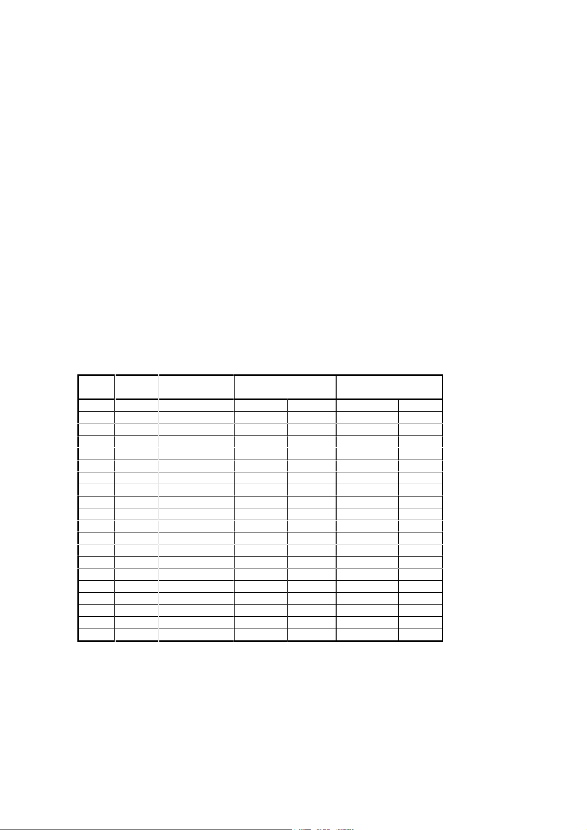
, 3UHGHILQHG)DFWRU\0RGHV
0RGH1R&KURPD
7LPLQJ
[
[
[
[
[
[
[
[
[
[
[
[ ,QW
[
[
[
[
[
UHVHUYHG
UHVHUYHG
86(502'(
5HVROXWLRQ
3L[HOV[/LQHV
+RUL]RQWDO
)UHTN+]3RODULW\
9HUWLFDO
)UHT+]3RODULW\
1. Predefined Factory Modes
Mode No Chroma Timing Resolution
(Pixels x Lines) Horizontal
Freq.(kHz) Polarity Vertical
Freq.(Hz) Polarity
0 105 720x400 31.469 - 70.087 +
1 106 720x400 37.927 - 85.039 +
2 107 640x480 31.469 - 59.940 3 108 640x480 37.861 - 72.809 4 109 640x480 37.500 - 75.000 5 110 640x480 43.269 - 85.008 -
2

6 111 800x600 35.156 + 56.250 +
7 112 800x600 37.879 + 60.317 +
8 113 800x600 48.077 + 72.188 +
9 114 800x600 46.875 + 75.000 +
10 115 800x600 53.674 + 85.061 +
11 116 1024x768 35.5 + 43.479 Int. +
12 117 1024x768 48.363 - 60.004 13 118 1024x768 56.476 - 70.069 14 119 1024x768 60.023 + 75.029 +
15 120 1024x768 68.677 + 84.997 +
16 121 1280x1024 63.981 + 60.020 +
17 reserved
18 reserved
19 USER MODE
SINGLE/MULTISTANDARD VIF/SIF-PLL and FM-PLL/AM DEMODULATOR TDA9818 ....................................................... 6
COMB FILTER SAA4961 ......................................................................................................................................................... 6
POWER SUPPLY (SMPS) ....................................................................................................................................................... 6
MICROCONTROLLER SDA525X ............................................................................................................................................ 6
SERIAL ACCESS CMOS 8K (1024*8) EEPROM ST24C08 ................................................................................................... 6
CLASS AB STEREO HEADPHONE DRIVER TDA1308 ......................................................................................................... 7
SAW FILTERS .......................................................................................................................................................................... 7
IC DESCRIPTIONS AND INTERNAL BLOCK DIAGRAM ....................................................................................................... 7
TDA8840/TDA8842/TDA8844 ........................................................................................................................................... 7-8
UV1315/UV1316/UV1336 .................................................................................................................................................. 9-10
TEA6415C .......................................................................................................................................................................... 10
TDA9830 ............................................................................................................................................................................ 10
TDA2614/TDA2615/TDA2616Q......................................................................................................................................... 11-12
TDA8351/TDA8356 ............................................................................................................................................................ 12
TDA6107Q ......................................................................................................................................................................... 13
SAA4961 ............................................................................................................................................................................ 13-14
MC44604 ............................................................................................................................................................................ 14-15
SDA525X ............................................................................................................................................................................ 16-17
TDA9875 ............................................................................................................................................................................ 17-18
TDA9818 ............................................................................................................................................................................ 18
ST24C08 ............................................................................................................................................................................ 18
TDA1308 ............................................................................................................................................................................ 18
G1965M .............................................................................................................................................................................. 18
TDA9855 ............................................................................................................................................................................ 19
AK19 CHASSIS MANUAL ADJUSTMENT PROCEDURE ...................................................................................................... 20
For Adjust Settings............................................................................................................................................................. 20
WHITE BALANCE ADJUSTMENT .................................................................................................................................... 20
AGC ADJUSTMENT .......................................................................................................................................................... 20
IF-PLL NEGATIVE ADJUSTMENT .................................................................................................................................... 20
IF-PLL POSITIVE ADJUSTMENT ..................................................................................................................................... 20
LUMINANCE DELAY ADJUSTMENT ................................................................................................................................ 20
VERTICAL ZOOM ADJUSTMENT .................................................................................................................................... 20
VERTICAL SCROLL ADJUSTMENT ................................................................................................................................. 20
4 : 3 HORIZONTAL SHIFT ADJUSTMENT ................................................................................................................... 20
4 : 3 VERTICAL SLOPE ADJUSTMENT ....................................................................................................................... 20
4 : 3 VERTICAL AMPLITUDE ADJUSTMENT .............................................................................................................. 21
4 : 3 S-CORRECTION ADJUSTMENT .......................................................................................................................... 21
4 : 3 VERTICAL SHIFT ADJUSTMENT ......................................................................................................................... 21
4 : 3 EW WIDTH ADJUSTMENT ................................................................................................................................... 21
4 : 3 EW PARABOLA WIDTH ADJUSTMENT .............................................................................................................. 21
4 : 3 EW CORNER PARABOLA ADJUSTMENT ........................................................................................................................ 21
4 : 3 EW TRAPEZIUM ADJUSTMENT ........................................................................................................................................ 21
16 : 9 HORIZONTAL SHIFT ADJUSTMENT ................................................................................................................................. 21
16 : 9 VERTICAL SLOPE ADJUSTMENT ..................................................................................................................................... 21
16 : 9 VERTICAL AMPLITUDE ADJUSTMENT ........................................................................................................................... 21
16 : 9 S-CORRECTION ADJUSTMENT ......................................................................................................................................... 21
16 : 9 VERTICAL SHIFT ADJUSTMENT ....................................................................................................................................... 21
16 : 9 EW WIDTH ADJUSTMENT .................................................................................................................................................. 21
16 : 9 EW PARABOLA WIDTH ADJUSTMENT ........................................................................................................................... 21
16 : 9 EW CORNER PARABOLA ADJUSTMENT ....................................................................................................................... 22
16 : 9 EW TRAPEZIUM ADJUSTMENT ....................................................................................................................................... 22
For Option Settings ..................................................................................................................................................................................... 22
OPTION 00 .......................................................................................................................................................................................... 22
OPTION 01 .......................................................................................................................................................................................... 23
OPTION 02 .......................................................................................................................................................................................... 23
OPTION 03 .......................................................................................................................................................................................... 23-24
OPTION 04 .......................................................................................................................................................................................... 24
OPTION 05 .......................................................................................................................................................................................... 24
OPTION 06 .......................................................................................................................................................................................... 24
OPTION 07 .......................................................................................................................................................................................... 24-25
OPTION 08 .......................................................................................................................................................................................... 25
OPTION 09 .......................................................................................................................................................................................... 25
OPTION 10 .......................................................................................................................................................................................... 25
3
GENERAL BLOCK DIAGRAM OF CHASSIS AK19 .............................................................................................................................. 26
ELECTRONIC COMPONENT PART LIST ............................................................................................................................................... 27-28
DO NOT CHANGE ANY MODULE UNLESS THE SET IS SWITCH OFF
The mains supply side of the switch mode power supply transformer is live.
Use
Mid Band E to PP 145.25 to 391.25
High Band QQ to 69 397.25 to 801.25
Noise is typically 6dB for all channels. Gain is minimum 38dB and maximum 50dB for all channels.
Channel Coverage of UV1315:
BAND
OFF-AIR CHANNELS CABLE CHANNELS
CHANNELS FREQUENCY CHANNELS FREQUENCY
RANGE (MHz) RANGE (MHz)
Low Band E2 to C 48.25 to 82.25 (1) S01 to S10 69.25 to 168.25
Mid Band E5 to E12 175.25 to 224.25 S11 to S39 231.25 to 447.25
High Band E21 to E69 471.25 to 855.25 (2) S40 to S41 455.25 to 463.25
(1). Enough margin is available to tune down to 45.25 MHz.
(2). Enough margin is available to tune up to 863.25 MHz.
Noise Typ. Max. Gain Min. Typ. Max.
Low band : 6dB 9dB All Channels 38dB 44dB 50dB
Mid band : 6dB 10dB Gain Taper - - 8dB
High band : 6dB 11dB (off-air channels)
4.VIDEO SWITCH TEA6415C
In case of three or more external sources are used, the video switch IC TEA6415C is used. The main function of this device is to switch
8 video input sources on the 6 outputs.
Each output can be switched on only one of each input. On each input an alignment of the lowest level of the signal is made (bottom
of sync. top for CVBS or black level for RGB signals).
Each nominal gain between any input and output is 6.5dB.For D2MAC or Chroma signal the alignment is switched off by forcing, with
an external resistor bridge, 5VDC on the input. Each input can be used as a normal input or as a MAC or Chroma input (with external
resistor bridge). All the switching possibilities are changed through the BUS.
Driving 75ohm load needs an external resistor.
It is possible to have the same input connected to several outputs.
5. AM DEMODULATOR TDA9830
The TDA9830 is designed for AM-sound demodulation used in L and L standard.
Sound IF Input:
The sound IF amplifier consists of three AC-coupled differential amplifier stages each with approximately 20dB gain.
At the output of each stage is a multiplier for gain controlling. The overall control range is approximately -6 to +60dB and the
frequency response (-3dB) of the IF amplifier is approximately 6 to 70MHz. The steepness of gain control is approximately 10mV/dB.
IF AGC:
The automatic gain control voltage to maintain the AM demodulator output signal at a constant level is generated by a mean
level detector.The AGC-detector charges and discharges the capacitor at pin 3 controlled by the output signal of the
AM-demodulator compared to an internal reference voltage.The maximum charge/discharge current is approximately 5 mA.
AM-demodulator
The IF amplifier output signal is fed to a limiting amplifier (two stages) and to a multiplier circuit.
However the limiter output signal (which is not any more AM modulated) is also fed to the multiplier, which provides AM
demodulation (in phase demodulation). After lowpass filtering (fg @ 400kHz) for carrier rejection and buffering,
the demodulator output signal is present at pin 6.
Audio Switch
This circuit is an operational amplifier with three input stages and internal feedback network determining gain (0dB) and
frequency response (fg @ 700kHz). Two of the input stages are connected to pin 7 and pin 9, the third input stage to an
internal reference voltage. Controlled by the switching pins 10 and 12, one of the three input stages can be activated and a
choice made between two different AF signals or mute state. The selected signal is present at pin 8. The decoupling capacitors
at the input pins are needed, because the internally generated bias voltage for the input stages must not be influenced
by the application in order to avoid DC-plop in case of switching.
Reference Circuit:
This circuit is a band gap stabiliser in combination with a voltage regulation amplifier, which provides an internal reference voltage
of about 3.6V nearly independent from supply voltage and temperature. This reference voltage is filtered by the capacitor at
pin 4 in order to reduce noise. It is used as a reference to generate all important voltages and currents of the circuit.
4

For application in 12V power supply concepts, there is an internal voltage divider in combination with a Darlington transistor in
order to reduce the supply voltage for all IC function blocks to approximately 6V.
6. DIGITAL TV SOUND PROCESSOR TDA9875
The TDA9875 is a single-chip Digital TV Sound Processor.
Supported standards are M, B/G, D/K, I and L.
Description of the demodulator and decoder section:
SIF Input:
Two input pins are provided, SIF1 e.g. for terrestrial TV and SIF2 e.g. for a satellite tuner. The selected signal is passed through an
AGC circuit and then digitized by an 8-bit ADC operating at 24.576MHz.
AGC:
The gain of the AGC amplifier is controlled from the ADC output by means of a digital control loop employing hysteresis.
The AGC has a fast attack behaviour to prevent ADC overloads and slow decay behaviour AGC oscillations.
For AM demodulation AGC must be switched off.
Mixer
The digitized input signal is fed to the mixers, which mix one or both input sound carriers down to zero IF. A 24-bit control word for
each carrier sets the required frequency.
FM and AM Demodulation
An FM or AM input signal is fed via a band-limiting filter to a demodulator that can be used for either FM or AM demodulation.
Apart from the standard (fixed) de-emphasis characteristic, an adaptive de-emphasis is available for encoded satellite programs.
A stereo decoder recovers the left and right signal channels from the demodulated sound carriers.
FM Identification:
The identification of the FM sound mode is performed by AM synchronous demodulation of the pilot signal and narrow-band detection
of the identification frequencies. The result is available via the I²C-bus interface.
NICAM Demodulation:
The NICAM signal is transmitted in a DQPSK code at a bit rate of 728 kbit/s. The NICAM demodulator performs DQPSK
demodulation and feeds the resulting bitstream and clock signal onto the NICAM decoder and, for evaluation purposes, to PCLK
(pin 1) and NICAM (pin 2).
NICAM Decoder:
The device performs all decoding functions in accordance with the EBU NICAM 728 specification. After locking to the frame
alignment word, the data is descrambled by applying the defined pseudo-random binary sequence; the device will then synchronise
to the periodic frame flag bit C0.
The status of the NICAM decoder can be read out from the NICAM status register by the user. The OSB bit indicates that the
decoder has locked to the NICAM data. The VDSP bit indicates that the decoder has locked to the NICAM data and that the
data is valid sound data.
7. SOUND OUTPUT STAGE TDA2614/TDA2615/TDA2616Q
TDA2614 is used as the AF output amplifier for mono applications. It is supplied by ±12VDC coming from a separate winding in the
SMPS transformer. An output power of 2*6W (THD=0.5%) can be delivered into an 8ohm load.
TDA2615 is used as the AF output amplifier for stereo applications. It is supplied by
±12VDC coming from a separate winding in the SMPS transformer. An output power of 2*6W (THD=0.5%)
can be delivered into an 8ohm load.
TDA2616Q is used as the AF output amplifier for stereo and dolby prologic applications. It is supplied by ±16VDC coming from
a separate winding in the SMPS transformer. An output power of 2*12W (THD=0.5%) can be delivered into an 8ohm load.
8. VERTICAL OUTPUT STAGE WITH TDA8351/8356
The TDA8351/8356 vertical deflection circuit can be used in 90° and 110° deflection systems with field frequencies from
50 up to 120Hz. With its bridge configuration the deflection output can be DC coupled with few external components.
Only a single supply voltage for the scan and a second supply for the flyback are needed. The TDA8356 is intended for 90°
systems and the TDA8351 is intended for 110° systems.
The drive voltage is amplified by an amplifier and fed to two amplifiers, one is inverting and the other is a non inverting amplifier.
The outputs (pins 7 and 4) are connected to the series connection of the vertical deflection coil and feedback resistor Rsense
(R702//R703). The voltage across Rsense is fed via pin 9 to correction amplifier, to obtain a deflection current which is proportional
to the drive voltage. The supply voltage for the TDA8351/8356 is 15VDC at pin 3. The supply voltage generator has a separate
supply voltage of 45VDC at pin 6.
9. VIDEO OUTPUT AMPLIFIER TDA6107Q
The TDA6107Q consists of three monolithic video output amplifiers. The amplifier can be seen as an operational amplifier
with negative feedback.
The advantage of negative feedback is that the amplifier characteristics do not play an important role up to certain frequencies.
The internal flash diodes protect the amplifiers against flash over in the picture tube.
The only protections required at the cathode outputs are a flash resistor and a sparkgap.
The TDA6107Q has an internal thermal protection circuit which gives a decrease of the slew rate at high temperatures.
Furthermore, the device needs only one power supply voltage (Vdd).
In contrast to previous types of DMOS video amplifiers, all the external resistors (Rf, Ri and Ra) are integrated, so the gain is fixed
and saves 9 resistors.
Furthermore, the reference voltage is integrated, it saves a resistor divider and a decoupling capacitor. So, the replacement
value of the TDA6107Q is very high.
The TDA6107Q is provided with a black current data pin. Since TDA884X is used as drive device, no adjustments are required
for gain and black setting, as the TDA884X has I²C white point adjustment and black current set-up.
10. SINGLE/MULTISTANDARD VIF/SIF-PLL and FM-PLL/AM
DEMODULATOR TDA9818
5

The TDA9818is an IC for multistandard vision IF signal processing, sound AM and FM demodulation.
It is a gain controlled wide band VIF-amplifier (AC-coupled). It is applicable for IF frequencies of 38.9 MHz, 45.75 MHz and 58.75 MHz.
True synchronous demodulation is provided with active carrier regeneration. It has a VCO frequency which can be switchable
between L and L accent (alignment external) picture carrier frequency.
The TDA9818 has a SIF input for single reference QSS mode (PLL controlled). SIF AGC detector is to provide gain controlled
SIF amplifier. The AM demodulator is without extra reference circuit. The supply voltage is +5VDC at pin 21.
11. COMBFILTER SAA4961
The SAA 4961 is a one-chip, PAL/NTSC combfilter IC with internal delay lines, filters, clock control, synchronisation and
signal switches. The combfilter function is realised in a switched capacitor technique, so it has time discrete but amplitude
continuous processing.
The Y/CVBS input is first clamped and then fed to the delay-line and combfilter section via a low pass pre-filter.
This filter can be bypassed via the external LPF-on pin. This pin is internally pulled up, to put the filter default on. The Y/CVBs
input is also fed to the sync seperator, where horizontal and vertical reference pulses are made.
Bypass mode can be forced via BYP (pin 3).FSC (pin 1) is the subcarrier input which is connected to the colour decoder.
Input FSCSW pin indicates if fsc or 2*fsc is used.
The Sys1,2 pins (20, 23) indicate which system standard is processed. Sys2 is internally pulled up, Sys1 is internally pulled down.
Therefore when the Sys1,2 inputs are left open, automatically PAL 4.43MHz is forced.
SAA4961output pin 15 CVBS can be used for parallel-synced teletext decoders, to guarantee that the teletext display always
has a correct timing relation with the main picture. Comb filter is disabled by setting SAA4961 pin 3 BYP high.
12. POWER SUPPLY (SMPS)
The DC voltages required at various parts of the chassis are provided by an SMPS transformer controlled by the IC MC44604
which is designed for driving, controlling and protecting switching transistor of SMPS. The transformer produces 150/115V for
FBT input, ±14V for audio output IC, S+5V for microcontroller, +15V for vertical output (field scan) and +33V for tuner and some
other ICs and transistors.
13. MICROCONTROLLER SDA525X
The device is TV TEXT tuning and control system based on the SDA 525X TV TEXT microcontroller. It is designed for a low
cost mono TV-SET with analogue picture and sound control. Neverthless the system offers an on screen display (OSD) and
IR remote control of all functions.
SDA525X has the following features:
- Display of program number, channel number, TV standard, analogue values, sleep timer, parental control, and mute is done by OSD.
- Single LED for IR active, standby and on mode indication.
- 1 Control line to select external source.
- 3 Control lines for TV standard selection.
- Frequency synthesis tuning (62.5 kHz steps)
- 192 step fine tuning
- Channels corresponding to standards B/G, OIRT, L and I (I+)
- Mono sound control by analogue voltage
- System configuration with service mode
14. SERIAL ACCESS CMOS 8K (1024*8) EEPROM ST24C08
The ST24C08 is a 8Kbit electrically erasable programmable memory (EEPROM), organised as 4 blocks of 256*8 bits.
The memory is compatible with the I²C standard, two wire serial interface which uses a bi-directional data bus and serial clock.
The memory carries a built-in 4 bit, unique device identification code (1010) corresponding to the I²C bus definition.
This is used together with 1 chip enable input (E) so that up to 2*8K devices may be attached to the I²C bus and selected individually.
15. CLASS AB STEREO HEADPHONE DRIVER
The TDA1308 is an integrated class AB stereo headphone driver contained in a DIP8 plastic package.
The device is fabricated in a 1 mm CMOS process and has been primarily developed for portable digital audio applications.
16. SAW FILTERS
Saw filter type : Model:
G1965M : PAL-SECAM B/G MONO
G3962M : PAL-SECAM B/G GER&NIC STEREO, PAL I NIC STEREO, INT-1
G1984 : PAL-SECAM B/G GER&NIC STEREO INT-2
J1951M : PAL-I MONO
J3950M : PAL-I NIC STEREO
J1956M : PAL-I MONO
K2955M : PAL-SECAM B/G-D/K MONO, PAL-SECAM B/G-D/K-I, MONO, PAL-SECAM B/G-D/K-L MONO
K2958M : PAL-SECAM B/G-D/K (38) MONO
K2962M : PAL-SECAM B/G-L/L MONO
G3957M : PAL-SECAM B/G-L/L GER&NIC BG/L STEREO
K6256K : PAL-SECAM B/G-D/K-I-L/L MONO, PAL-SECAM B/G-D/K-I, L/L GER&NIC BG/L STEREO,
PAL-SECAM B/G-D/K-I-L/L I, NICAM STEREO, PAL-SECAM B/G-D/K-I-L/L GER&NIC I-B/G-L, STEREO
K6259K : PAL-SECAM B/G-D/K-I-M/N (EURO) MONO
M1963M : PAL M/N MONO, NTSC M MONO, PAL M/N-NTSC M MONO
TDA1308
17. BTSC STEREO/SAP/DBX-DECODER and AUDIO PROCESSOR TDA9855
The TDA9855 is a BTSC stereo/SAP/dbx decoder and audio processor. It performs all functions to transform the composite baseband
signal into the appropriate audio output signals to line out and to the loudspeaker output stages.
IC DESCRIPTIONS AND INTERNAL BLOCK DIAGRAM
n TDA8840/8842/8844
n TUNER (UV1315, UV1316, UV1336)
6

n TEA6415C
n TDA9830
n TDA2614/2615/2616Q
n TDA8351/8356
n TDA6107Q
n SAA4961
n MC44604
n SDA525X
n TDA9875
n TDA9818
n ST24C08
n TDA1308
n G1965M
n TDA9855
TDA8840/8842/8844:
The TDA884X is IýC-bus controlled single chip TV processor which is intended to be applied in PAL, NTSC, PAL/NTSC and
multi-standard television receivers. These IC s are nearly pin compatible with the TDA837X TV processors but have a higher
degree of integration because the delay line (TDA4665 function) and the SECAM decoder have been integrated. In addition to
these functions some additional features have been added like Continuous Cathode Calibration (2-point black current loop
which results in an accurate biasing of the 3 guns), adjustable luminance delay time, blue stretching and dynamic skin tone control.
Features:
n Vision IF circuit with PLL demodulator
n Alignment-free multi-standard FM sound demodulator (4.5 MHz to 6.5 MHz)
n Audio switch
n Flexible source selection with CVBS switch and Y(CVBS)/C input so that a comb filter can be applied
n Integrated chrominance trap circuit
n Integrated luminance delay line
n Asymmetrical peaking in the luminance channel with a noise coring function
n Black stretching of non-standard CVBS or luminance signals
n Integrated chroma band-pass filter with switchable center frequency
n Blue stretch circuit which offsets colours near white towards blue
n RGB control circuit with Continuous Cathode Calibration and white point adjustment
n Linear RGB inputs and fast blanking
n Possibility to insert a blue black option when no video signal is available
n Horizontal synchronisation with two control loops and alignment-free horizontal oscillator
n Vertical count-down circuit
n Vertical driver optimised for DC-coupled vertical output stages
n IýC-bus control of various functions
n Low dissipation (850 mW)
Functional Differences between the 8840/8842/8844:
IC VERSION (TDA) 8840 8842 8844
Multi-standard IF X X
Automatic Volume Limiting X X
PAL Decoder X X X
SECAM Decoder X X
NTSC Decoder X X
Dynamic Skin Control X
Colour Matrix PAL/NTSC (Japan) X X
Colour Matrix NTSC Japan/USA
YUV interface X
Base-band delay line X X X
Adjustable luminance delay time X
Horizontal geometry X
Horizontal and vertical zoom X
Vertical scroll X
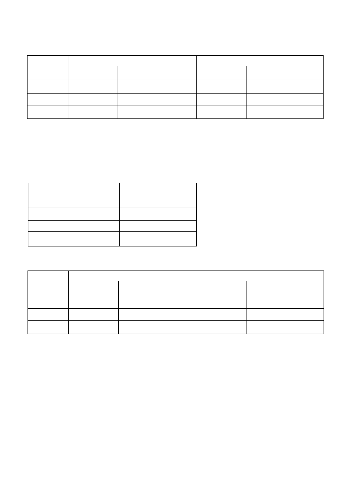
PINNING PIN VALUE
1. Sound IF input : 1mVrms
2. External audio input : 500mVrms
3. IF demodulator tuned circuit 1
4. IF demodulator tuned circuit 2
5. IF-PLL loop filter : Min:32-Max:60 MHz
6. IF video output : 4.7V (Negative Modulation), 2V (Positive Modulation)
7. Serial clock input : Low level max:1.5 V, High level min 3.5V
8. Serial data input/output : Low level max:1.5 V, High level min 3.5V
9. Bandgap decoupling
10. Chrominance input (S-VHS) : 1Vpp, Max:1.4Vpp
11. External CVBS/Y input : 1Vpp, Max:1.4Vpp
7

12. Main supply voltage 1 : 8V, Min:7.2V, Max:8.8V
13. Internal CVBS input : 1Vpp, Max:1.4Vpp
14. Ground 1
15. Audio output : 700mVrms, Min:500mVrms, Max:900mVrms
16. SECAM PLL decoupling
17. External CVBS input : Vpp, Max:1.4Vpp
18. Black-current input : Amplitude of low reference current : 8mA
Amplitude of high reference current : 20mA
19. Blue output : 2Vpp
20. Green output : 2Vpp
21. Red output : 2Vpp
22. Beam current limiter input/V-guard input
23. Red input for insertion : 0.7Vpp, Max:0.8Vpp
24. Green input for insertion : 0.7Vpp, Max:0.8Vpp
25. Blue input for insertion : 0.7Vpp, Max:0.8Vpp
26. RGB insertion input : Max:0.3V
27. Luminance input : 1.4Vpp
28. Luminance output : 1.4Vpp
29. (B-Y) signal output : 1.05Vpp
30. (R-Y) signal output : 1.05Vpp
31. (B-Y) signal input : 1.05Vpp
32. (R-Y) signal input : 1.05Vpp
33. Subcarrier reference output : 3.58/4.43 MHz
34. 3.58 MHz crystal connection
35. 4.43/3.58 MHz crystal connection
36. Loop filter phase detector
37. 2nd
38. CVBS output : 1Vpp, Max:1.4Vpp
39. Decoupling digital supply : 1.8V
40. Horizontal output : Max: 0.3V
41. Flyback input/sandcastle output : Min:100ma, Max:300mA
42. Phase-2 filter : 150 ms/ms
43. Phase-1 filter : ±0.9 kHz, Max: ±1.2 kHz
44. Ground 2
45. East-west drive output
46. Vertical drive A output : 0.95mA
47. Vertical drive B output : 0.95mA
48. IF input 1
49. IF input 2
50. EHT/overvoltage protection input : Min:1.2V, Max : 2.8V
51. Vertical sawtooth capacitor : 3Vpp
52. Reference current input : 3Vpp
53. AGC decoupling capacitor
54. Tuner AGC output : Max:9V (Maximum tuner AGC
55. Audio deemphasis : 500mVrms
56. Decoupling sound demodulator
supply voltage 1 : 8V, Min:7.2V, Max:8.8V
output voltage), 300mV (Output saturation voltage)
UV1315, UV1316, UV1336
General description of UV1315:
The UV1315 tuner belongs to the UV 1300 familiy of tuners, which are designed to meet a wide range of applications.
It is a combined VHF, UHF tuner suitable for CCIR systems B/G, H, L, L, I and I. The low IF output impedance has been
designed for direct drive of a wide variety of SAW filters with sufficient suppression of triple transient.
Features of UV1315:
n Member of the UV1300 family small sized UHF/VHF tuners
n Systems CCIR:B/G, H, L, L, I and I; OIRT:D/K
n Voltage synthesized tuning (VST)
n Off-air channels, S-cable channels and Hyperband
n Standardized mechanical dimensions and pinning
n Compact size
PINNING PIN VALUE
1. Gain control voltage (AGC) : 4.0V, Max:4.5V
2. Tuning voltage
3. High band switch : 5V, Min:4.75V, Max:5.5V
4. Mid band switch : 5V, Min:4.75V, Max:5.5V
5. Low band switch : 5V, Min:4.75V, Max:5.5V
6. Supply voltage : 5V, Min:4.75V, Max:5.5V
7. Not connected
8. Not connected
9. Not connected
10. Symmetrical IF output 1
11. Symmetrical IF output 2
8

Bandswitching table:
Pin 3 Pin 4 Pin 5
Low band 0V 0V +5V
Mid band 0V +5V 0V
High band +5V 0V 0V
General description of
The UV1316 tuner belongs to the UV 1300 family of tuners, which are designed to meet a wide range of applications.
It is a combined VHF, UHF tuner suitable for CCIR systems B/G, H, L, L, I and I. The low IF output impedance has been designed
for direct drive of a wide variety of SAW filters with sufficient suppression of triple transient.
Features of UV1316:
n Member of the UV1300 family small sized UHF/VHF tuners
n Systems CCIR: B/G, H, L, L, I and I; OIRT: D/K
n Digitally controlled (PLL) tuning via IýC-bus
n Off-air channels, S-cable channels and Hyperband
n World standardized mechanical dimensions and world standard pinning
n Compact size
n Complies to CENELEC EN55020 and EN55013
PINNING PIN VALUE
1. Gain control voltage (AGC) : 4.0V, Max:4.5V
2. Tuning voltage
3. I²C-bus address select : Max:5.5V
4. I²C-bus serial clock : Min:-0.3V, Max:5.5V
5. I²C-bus serial data : Min:-0.3V, Max:5.5V
6. Not connected
7. PLL supply voltage : 5.0V, Min:4.75V, Max:5.5V
8. ADC input
9. Tuner supply voltage : 33V, Min:30V, Max:35V
10. Symmetrical IF output 1
11. Symmetrical IF output 2
UV1316:
General description of
UV1336 series is developed for reception of channels broadcast in accordance with the M, N standard. The tuning is available
through built-in digitally controlled IýC bus (PLL).
Features of UV1336:
n Global standard pinning
n Integrated Mixer-Oscillator&PLL function
n Conforms to CISPR 13, FCC and DOC (Canada) regulations
n Low power consumption
n Both Phono connector and F connector are available
PINNING PIN VALUE
1. Gain control voltage : 4.0V, Max:4.5V
2. Tuning voltage
3. Address select : Max:5.5V
4. Serial clock : Min:-0.3V, Max:5.5V
5. Serial data : Min:-0.3V, Max:5.5V
6. Not connected
7. Supply voltage : 5.0V, Min:4.75V, Max:5.5V
8. ADC input (optional)
9. Tuning supply voltage : 33V, Min:30V, Max:35V
10. Ground
11. IF output
UV1336:
TEA6415C:
General Description:
The main function of the TEA6415C is to switch 8 video input sources on the 6 outputs.
Each output can be switched to only one of the inputs whereas but any same input may be connected to several outputs.
All switching possibilities are controlled through the IýC-bus.
Features:
n 20 MHz Bandwith
n Cascadable with another TEA6415C (Internal address can be changed by pin 7 voltage)
n 8 inputs (CVBS, RGB, Mac, CHROMA, )
n 6 Outputs
n Possibility of MAC or chroma signal for each input by switching-off the clamp with an external resistor bridge
n Bus controlled
n 6.5dB gain between any input and output
n -55dB crosstaljk at 5MHz
9
 Loading...