

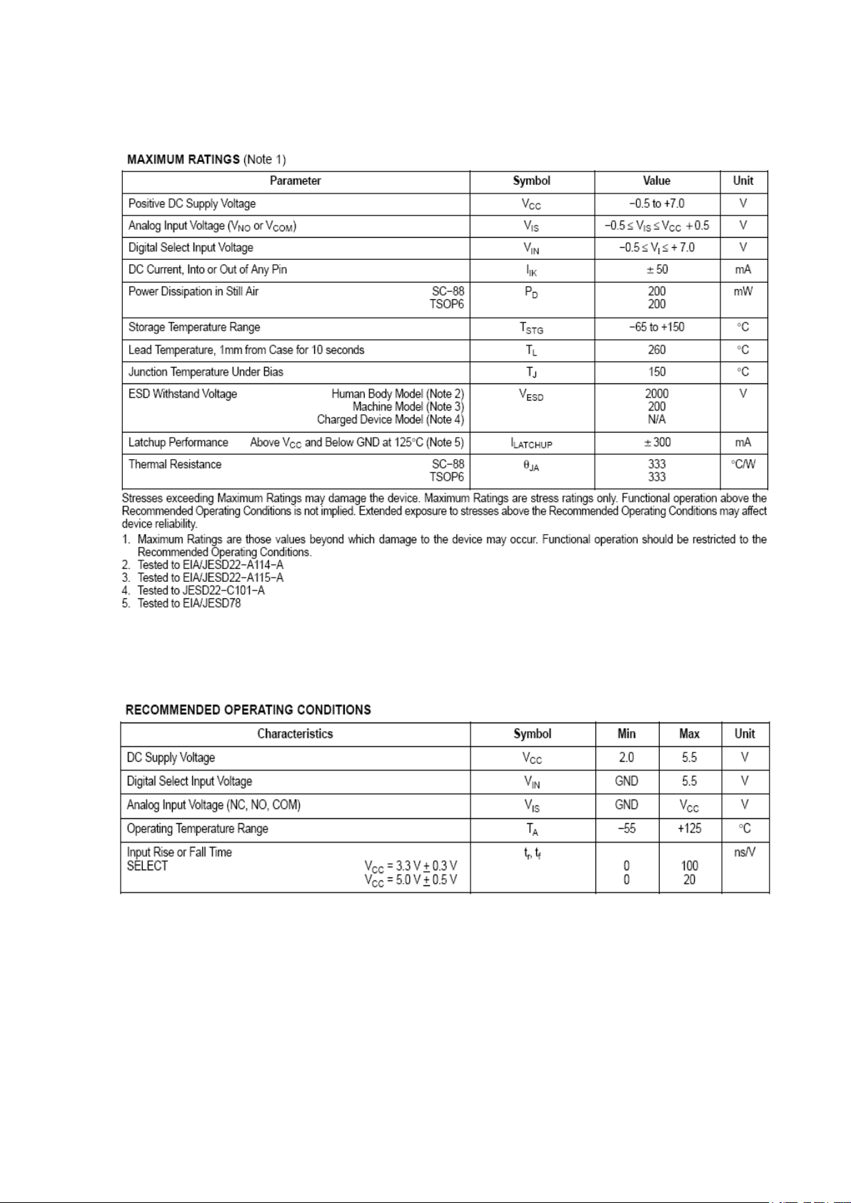
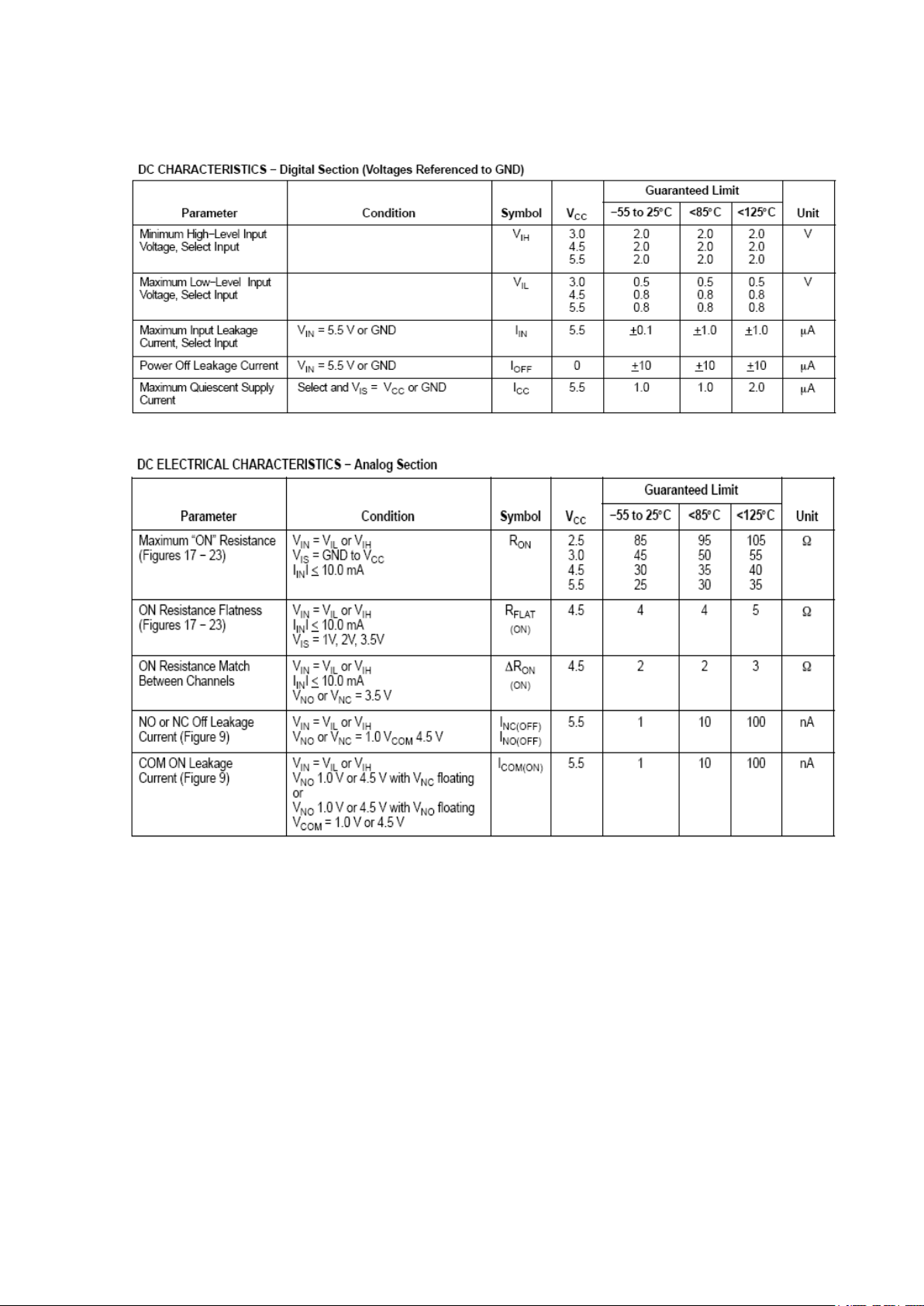
VESTEL 11AK58 Schematic

TABLE OF CONTENTS
1. INTRODUCTION.....................................................................................................3
1.1. Purpose ...............................................................................................................................3
1.2. Scope ..................................................................................................................................3
1.3. General Features...................................................................................................................3
2. GENERAL DESCRIPTION .....................................................................................4
2.1. Introduction .........................................................................................................................4
2.2. System Building Blocks ..........................................................................................................5
2.2.1. AK58 Chassis Block Diagrams 5
2.2.1.1. Genaral ..............................................................................................................5
2.2.1.2. SMPS..................................................................................................................5
2.2.1.3. AK58 OUTPUT SWTICTHING TABLE.......................................................................6
2.2.1.4. DEFLECTION .......................................................................................................7
2.2.2. AK58 Chassis Main Blocks 8
2.2.2.1. UOC-II (ULTIMATE-ONE-CHIP)..............................................................................8
2.2.2.2. Audio ...............................................................................................................18
2.2.2.3. External AV I/O .................................................................................................21
2.2.2.4. AV Switching .....................................................................................................22
2.2.2.4.1. MC74VHC4052............................................................................................... 22
2.2.2.4.2. NLAST4599 ................................................................................................... 25
2.2.2.5. TUNER .............................................................................................................29
2.2.2.6. SAW FILTERS .................................................................................................... 31
2.2.2.6.1. K3958M (IF Filter for Video Applications) ..........................................................31
2.2.2.6.2. K9656M (IF Filter for Audio Applications) .......................................................... 31
2.2.2.6.3. K2966 (IF Filter for Intercarrier Applications)..................................................... 32
2.2.2.6.4. K2962 (IF Filter for Intercarrier Applications)..................................................... 33
2.2.2.6.5. G1975 (IF Filter for Intercarrier Applications) ....................................................34
2.2.2.7. SMPS................................................................................................................ 34
2.2.2.7.1. PRIMARY BLOCK............................................................................................ 34
2.2.2.7.1.1. SMPS CONTROLLER (NCP1207) ....................................................................... 35
2.2.2.7.1.2. MOSFET........................................................................................................39
2.2.2.7.1.2.1. MTP3N60E ..................................................................................................39
2.2.2.7.1.2.2. MTP6N60E ..................................................................................................40
2.2.2.7.2. SECONDARY BLOCK .......................................................................................41
2.2.2.7.3. SMPS Block Diagram ......................................................................................42
2.2.2.8. DEFLECTION ..................................................................................................... 43
2.2.2.8.1. HORIZANTAL DEFLECTION .............................................................................43
2.2.2.8.2. MD1803DFX ..................................................................................................43
2.2.2.8.3. FBT .............................................................................................................. 45
2.2.2.8.4. AN15526A (VERTICAL DEFLECTION OUTPUT)................................................... 46
2.2.2.9. CRT BOARD ...................................................................................................... 50
2.2.3. AK58 Chassis Scematics 53
2.2.3.1. Part1 ................................................................................................................ 53
2.2.3.2. Part2 ................................................................................................................ 54
2.2.3.3. Part3 ................................................................................................................ 55
2.2.3.4. Part4 ................................................................................................................ 56
2.2.3.5. Part5 ................................................................................................................ 57
2.2.4. DVD PLAYER 58
2.2.4.1. General Description............................................................................................ 58
2.2.4.1.1. MT1389D ...................................................................................................... 58
2.2.4.1.2. SDRAM Memory Interface ............................................................................... 59
2.2.4.1.3. Drive Interfaces .............................................................................................59
2.2.4.2. System Block Diagram and MT1389D Pin Description.............................................60
2.2.4.2.1. MT1389D Pin Description ................................................................................60
2.2.4.2.2. 2.1 Sytem Block Diagram................................................................................69
2.2.4.3. Audio Output.....................................................................................................69
2.2.4.4. Audio DACS.......................................................................................................69
2.2.4.5. Video Interface..................................................................................................70
2.2.4.6. Flash Memory....................................................................................................71
2.2.4.7. Serial Eeprom Memory ....................................................................................... 71
2.2.4.8. Audio Interface Audio Sampling Rate and PLL Component Configuration..................71
2.2.4.9. Scematics ......................................................................................................... 72
2.2.4.9.1. Part1 ............................................................................................................72
2.2.4.9.2. Part2 ............................................................................................................73
2.2.4.9.3. Part3 ............................................................................................................75
2.2.4.9.4. Part4 ............................................................................................................76
2.2.4.9.5. Part 5 ...........................................................................................................77
2.3. AK58 Service Menu .............................................................................................................79
2.4. TUNER SETTINGS .................................................................................................................0
DOCUMENT HISTORY
Versi
Date
on
10/10/2007 Draft Yavuz INCE SERDAR GÜLTEN
File Name: AK58_HW_DOC
V00
Document
Revision and
Status Prepared by Approved by
Review
History

1. Introduction
1.1. Purpose
This document is prepared for the UOCII TV project and describes the whole system features
and operating principles to be used in hardware design phase.
The document is based on “Device Specification UOCII-Version 1.12” from
Semiconductors
Prior to hardware design start, all parties involved must agree with the contents of this
document.
.
Philips
1.2. Scope
The document covers detailed descriptions of 11AK58 chassis system building blocks.
1.3. General Features
11AK58 is a 90 / 50 Hz. chassis which is capable of driving 20” and 21” superflat and 21”
realflat CRT’s .
The chassis will have the following main features;
Remote Control
100 programs
On Screen Display
AV Stereo
Colour Standarts ; PAL, SECAM, NTSC,
Transmission standarts ; B/G, L/L’ I/I’, DK,
Teletext ; One pages,

Multi-standard alignment free PLL tuning,
DVD or DVIX Player
DVB-T option
2 Europe Scart (Scart1 is Full Scart)
Detachable headphone output option,
Front or side or back AV input option,
Back AV output option,
Coaxial output for IDTV/DVB-T
2* 2W (%10 THD),
90-270V 50Hz or 170V-270V 50Hz SMPS
Less than 3W
DVD-Video, DVD R/RW, CD-R/RW, CD-Audio and MP3 Audio, JPEG (Picture CD), Video CD
and its sub formats like CVD, SVCD, DVCD.
2. General Description
2.1. Introduction
This chapter describes system building blocks and their detailed descriptions.
2.2. System Building Blocks
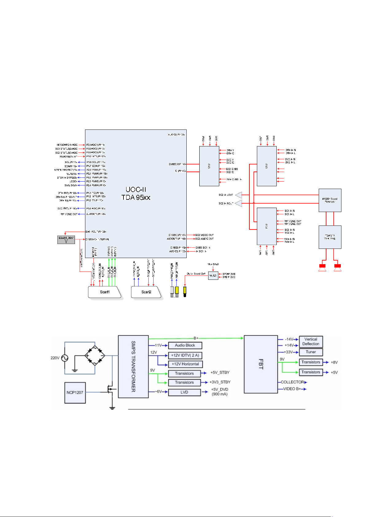
2.2.1. AK58 Chassis Block Diagrams
2.2.1.1. Genaral
2.2.1.2. SMPS
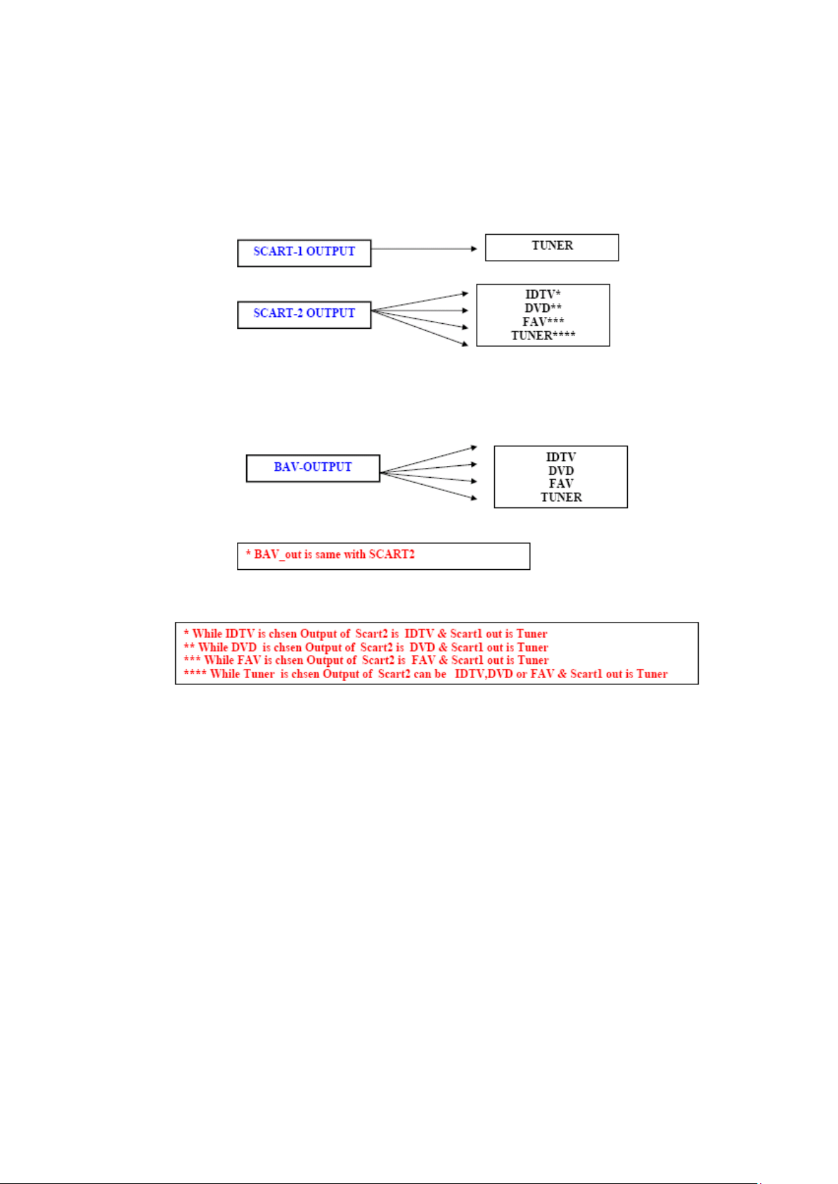
2.2.1.3. AK58 OUTPUT SWTICTHING TABLE
2.2.1.4. DEFLECTION
HORIZONTAL
DRIVE
+8V
+5V
-14V VERTICAL
+14V VERTICAL
RGB
DRIVE
HORIZONTAL
Horz.
Yoke
Lin.
+9V
CRT
TRANSISTORS
BOARD
Heater
30KV
FOCUS
SCREEN
+33V
Heater
30KV
G2 FOCUS
VERTICAL
DRIVE
VERTICAL
AMPLIFIER
AN5524A
VERTICAL
YOKE

2.2.2. AK58 Chassis Main Blocks
AK58 chassis main blocks are;
UOCII : Microcontroller + Video Proccessor + Sound Proccessor + IF + Teletext
AUDIO : Audio Amp.,
EXT. AV I/O : Scart1, Scart2 , AV input, AV output
AV SWITCHING : 4052, 4599
TUNER : PLL Tuner
SAW FILTERS
SMPS : SMPS Controller, SMT, Bridge Rect., Line Filters
DEFLECTION : FBT, HOT, Vertical Amplifier, Line Driver,
CRT BOARD : RGB Amp. with transistors,
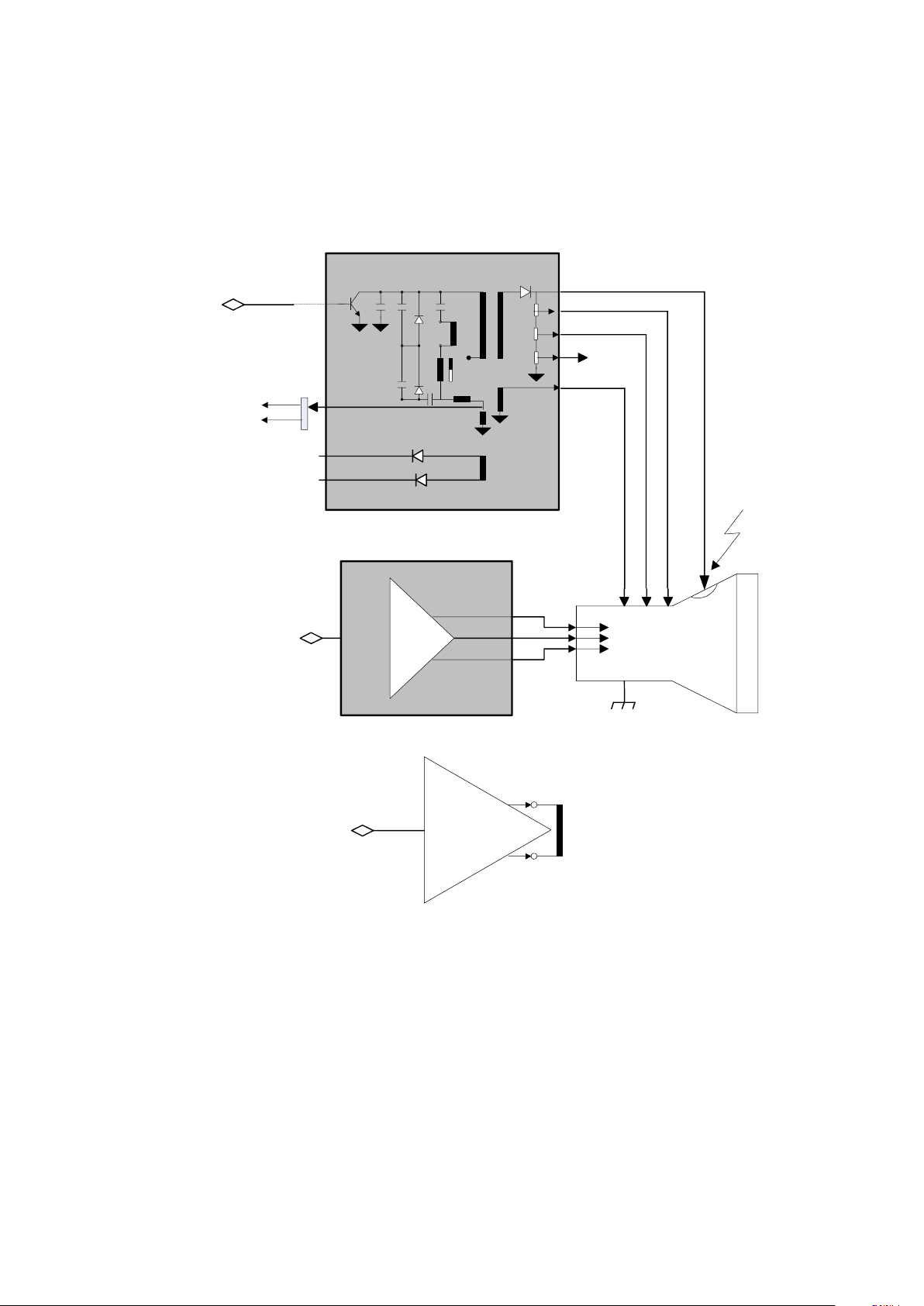
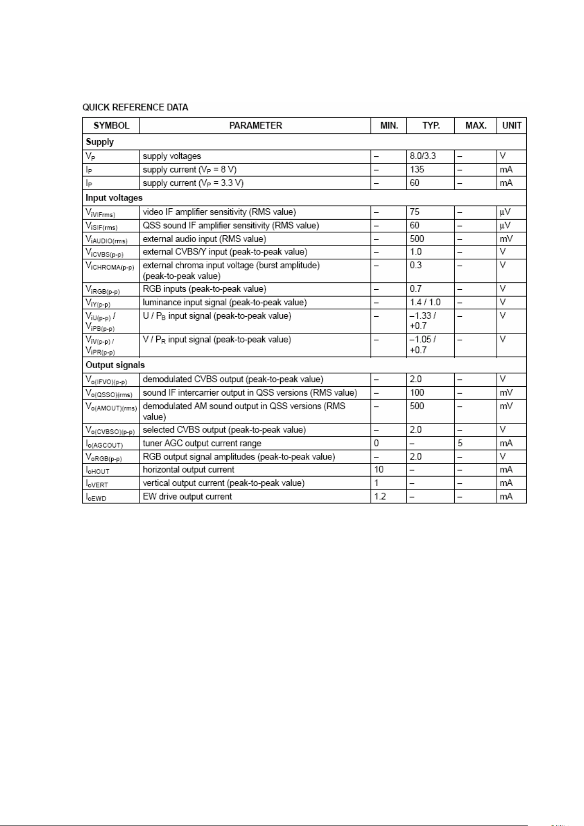
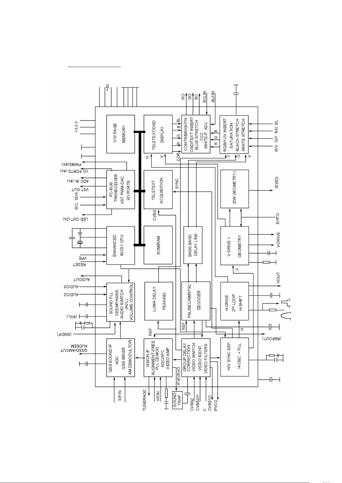
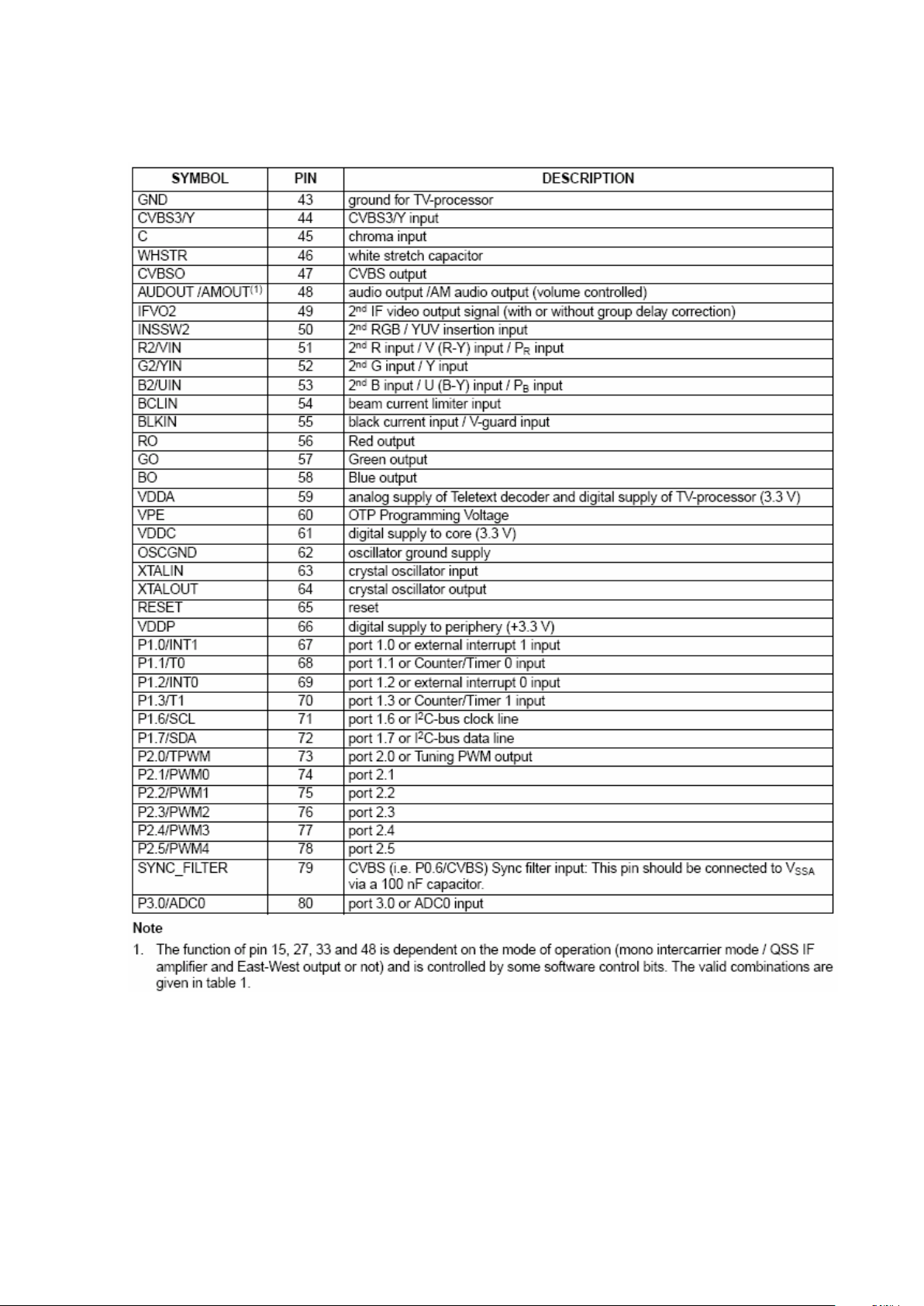
2.2.2.1. UOC-II (ULTIMATE-ONE-CHIP)
UOCII is composed of microcontroller, video proccessor, sound proccessor and IF blocks.
The various versions of the TDA955X H/N1 series combine the functions of a video processor
together with a microcontroller.The ICs are intended to be used in economy television receivers
with 90 and 110 degree picture tubes.
The ICs have supply voltages of 8V and 3.3V and they are mounted in a QFP 80 envelope.
The features are given in the following feature list.
FEATURES
TV-signal processor
Multi-standard vision IF circuit with alignment-free PLL demodulator
Internal (switchable) time-constant for the IF-AGC circuit

The QSS and mono FM functionality are both available so that an FM/AM TV receiver can
be built without the use of additional ICs
The mono intercarrier sound circuit has a selective
FM-PLL demodulator which can be switched to the different FM sound frequencies
(4.5/5.5/6.0/6.5 MHz). The quality of this system is such that the external band-pass
filters can be omitted.
The FM-PLL demodulator can be set to centre frequencies of 4.74/5.74 MHz so that a
second sound channel can be demodulated. In such an application it is necessary that an
external bandpass filter is inserted.
The vision IF and mono intercarrier sound circuit can be used for the demodulation of
FM radio signals
Video switch with 2 external CVBS inputs and a CVBS output. One of the CVBS inputs
can be used as Y/C input.
2 external audio inputs. The selection of the various inputs is coupled to the selection of
the CVBS signals
Integrated chrominance trap circuit
Integrated luminance delay line with adjustable delay time
Switchable group delay correction in the CVBS path
Picture improvement features with peaking (with switchable centre frequency,
depeaking, variable positive/negative overshoot ratio and video dependent coring),
dynamic skin tone control and blue-, black- and white stretching
Integrated chroma band-pass filter with switchable centre frequency
Switchable DC transfer ratio for the luminance signal
Only one reference (12 MHz) crystal required for the m-Controller, Teletext- and the
colour decoder
PAL/NTSC or multi-standard colour decoder with automatic search system
Internal base-band delay line
Indication of the Signal-to-Noise ratio of the incoming CVBS signal
A linear RGB/YUV/YPBPR input with fast blanking for external RGB/YUV sources. The
synchronisation circuit can be connected to the incoming Y signal. The Text/OSD signals
are internally supplied from the
m-Controller/Teletext decoder.

RGB control circuit with ‘Continuous Cathode Calibration’, white point and black level off-
set adjustment so that the colour temperature of the dark and the light parts of the
screen can be chosen independently.
Contrast reduction possibility during mixed-mode of OSD and Text signals
Adjustable ‘wide blanking’ of the RGB outputs
Horizontal synchronization with two control loops and alignment-free horizontal oscillator
Vertical count-down circuit
Vertical driver optimized for DC-coupled vertical output stages
Horizontal and vertical geometry processing
Horizontal and vertical zoom function for 16 : 9 applications
Horizontal parallelogram and bow correction for large screen picture tubes
Low-power start-up of the horizontal drive circuit
Microcontroller
80C51 m-controller core standard instruction set and timing
1 ms machine cycle
32 - 128Kx8-bit late programmed ROM
3 - 12Kx8-bit DataRAM (shared between Display, Acquisition and Auxiliary RAM)
Interrupt controller for individual enable/disable with two level priority
Two 16-bit Timer/Counter registers
One 16-bit Timer with 8-bit Pre-scaler
WatchDog timer
Auxiliary RAM page pointer
16-bit Data pointer
Stand-by, Idle and Power Down modes
14 bits PWM for Voltage Synthesis Tuning
8-bit A/D converter with 4 multiplexed inputs
5 PWM (6-bits) outputs for control of TV analogue signals
18 general I/O ports

Data Capture
Text memory for 1 or 10 pages
In the 10 page versions inventory of transmitted Teletext pages stored in the
Transmitted Page Table (TPT) and Subtitle Page Table (SPT)
Data Capture for US Closed Caption
Data Capture for 525/625 line WST, VPS (PDC system A) and Wide Screen Signalling
(WSS) bit decoding
Automatic selection between 525 WST/625 WST
Automatic selection between 625 WST/VPS on line 16 of VBI
Real-time capture and decoding for WST Teletext in Hardware, to enable optimized m-
processor throughput
Automatic detection of FASTEXT transmission
Real-time packet 26 engine in Hardware for processing accented, G2 and G3 characters
Signal quality detector for video and WST/VPS data types
Comprehensive teletext language coverage
Full Field and Vertical Blanking Interval (VBI) data capture of WST data
Display
Teletext and Enhanced OSD modes
Features of level 1.5 WST and US Close Caption
Serial and Parallel Display Attributes
Single/Double/Quadruple Width and Height for characters
Scrolling of display region
Variable flash rate controlled by software
Enhanced display features including overlining, underlining and italics
Soft colours using CLUT with 4096 colour palette
Globally selectable scan lines per row (9/10/13/16) and character matrix [12x10, 12x13,
12x16 (VxH)]
Fringing (Shadow) selectable from N-S-E-W direction
Fringe colour selectable
Meshing of defined area

Contrast reduction of defined area
Cursor
Special Graphics Characters with two planes, allowing four colours per character
32 software redefinable On-Screen display characters
4 WST Character sets (G0/G2) in single device (e.g. Latin, Cyrillic, Greek, Arabic)
G1 Mosaic graphics, Limited G3 Line drawing characters
WST Character sets and Closed Caption Character set in single device
Optional Used ICs at AK57 chassis are TDA9550 H/N1, TDA9551 H/N1, TDA9552 H/N1.
FUNCTIONALOF TDA9550 H/N1
TV range is 90°
Mono intercarrier multi-standard sound demodulator (4.5 - 6.5 MHz) with switchable
centre frequency Audio switch
Automatic Volume Levelling
PAL decoder
NTSC decoder
ROM size 32 – 64K
User RAM size 1K
One page teletext
Close Captioning
FUNCTIONALOF TDA9551H
TV range is 90°
Mono intercarrier multi-standard sound demodulator (4.5 - 6.5 MHz) with switchable
centre frequency Audio switch
Automatic Volume Levelling
PAL decoder
SECAM decoder
NTSC decoder
ROM size 32 – 64K

User RAM size 1K
One page teletext
Close Captioning
FUNCTIONALOF TDA9552H
TV range is 90°
Mono intercarrier multi-standard sound demodulator (4.5 - 6.5 MHz) with switchable
centre frequency Audio switch
Automatic Volume Levelling
QSS sound IF amplifier with separate input and AGC circuit
AM sound demodulator without extra reference circuit
PAL decoder
SECAM decoder
NTSC decoder
ROM size 32 – 64K
User RAM size 1K
One page teletext
Close Captioning
BLOCK DIAGRAM
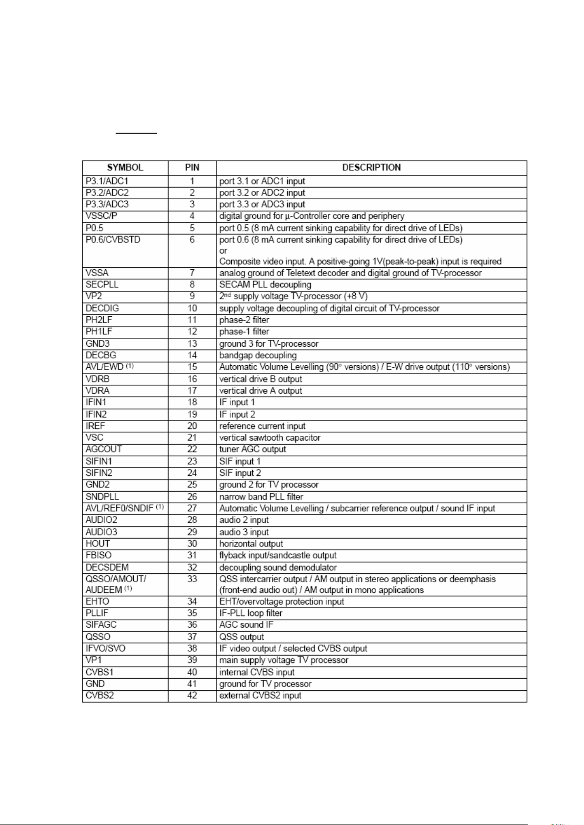
PINING
2.2.2.2. Audio
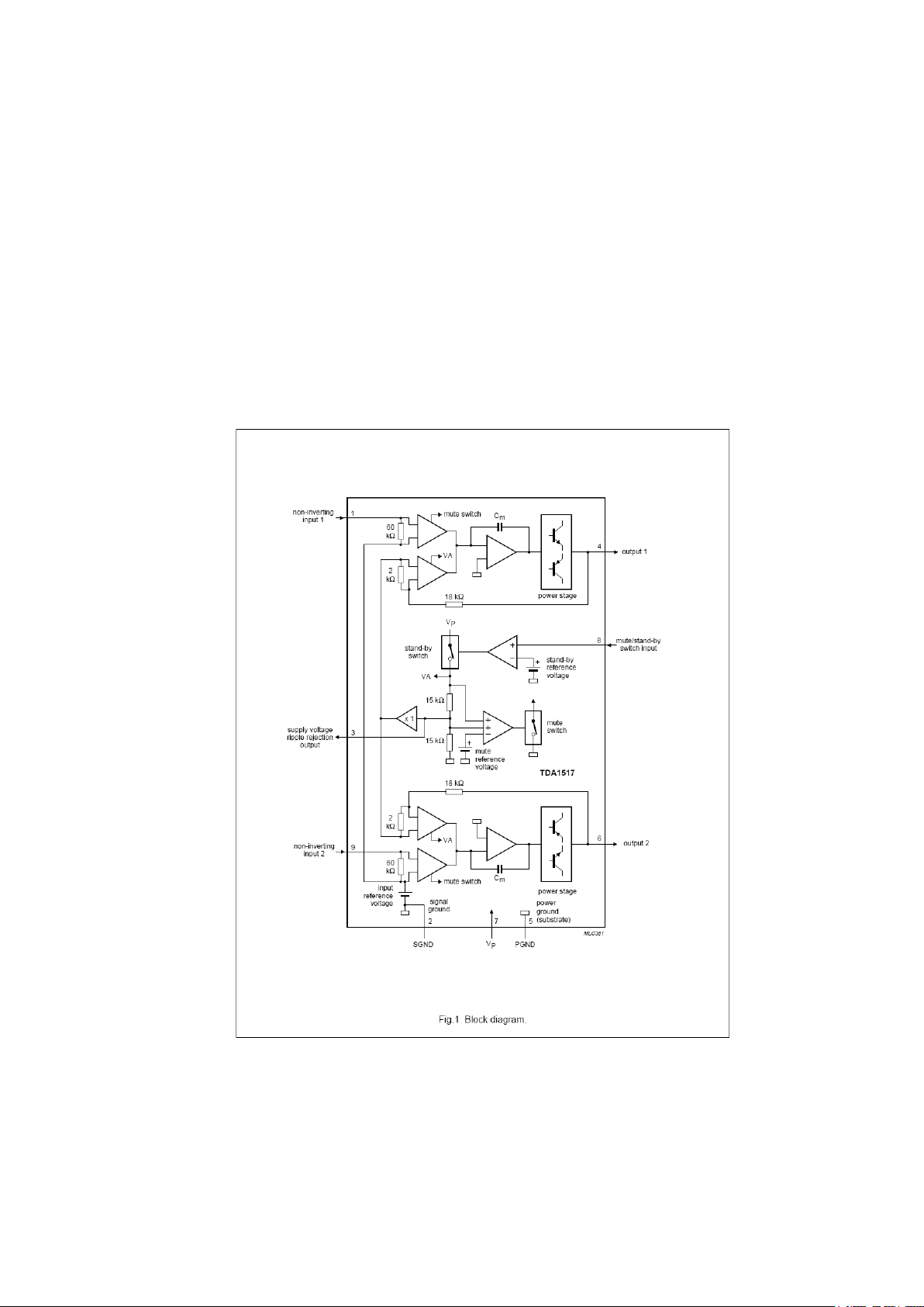
The TDA1517 stereo power amplifier.
Low crossover distorsion
Low quıescent current
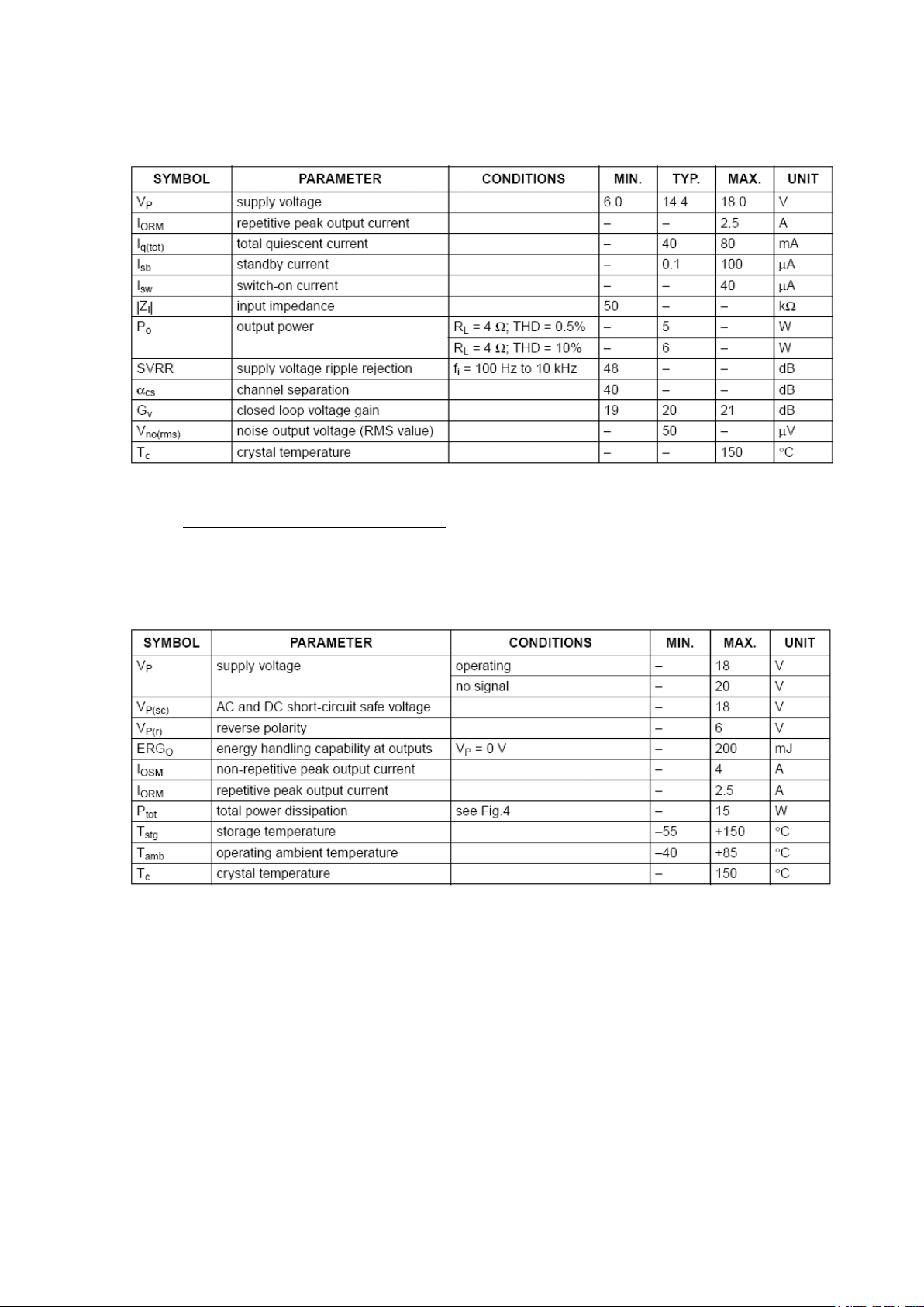
ELECTRICALCHARACTERISTICS
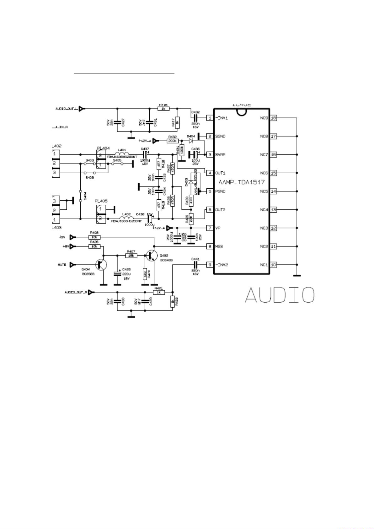
Figure: Application in 11AK58

2.2.2.3. External AV I/O
SCART PINING
1. Audio right output 0.5Vrms / 1KΩ
2. Audio right input 0.5Vrms / 10KΩ
3. Audio left output 0.5Vrms / 1KΩ
4. Ground AF
5. Ground Blue
6. Audio left input 0.5Vrms / 10K
Ω
7. Blue input 0.7Vpp / 75Ω
8. AV switching input 0-12VDC /10KΩ
9. Ground Green
10. Not Used
11. Green input 0.7Vpp / 75
Ω
12. Not Used
13. Ground Red
14. Ground Blanking
15. Red input 0.7Vpp / 75
Ω
16. Blanking input 0-0.4VDC, 1-3VDC / 75Ω
17. Ground CVBS output
18. Ground CVBS input
19. CVBS output 1Vpp / 75
Ω
20. CVBS input 1Vpp / 75Ω
21. Ground

Front/Side/Back AV Input
Audio 0.5Vrms / 10KΩ
Video 1Vpp / 75Ω
Back AV Output
Audio 0.5Vrms / 1KΩ
Video 1Vpp / 75Ω
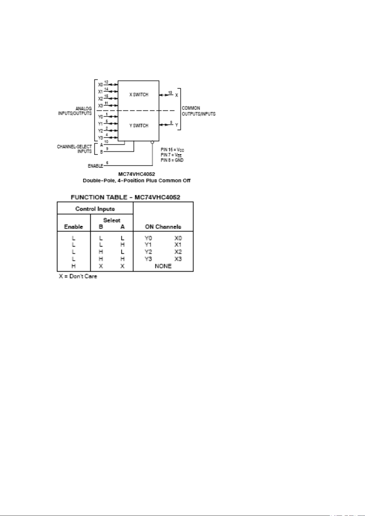
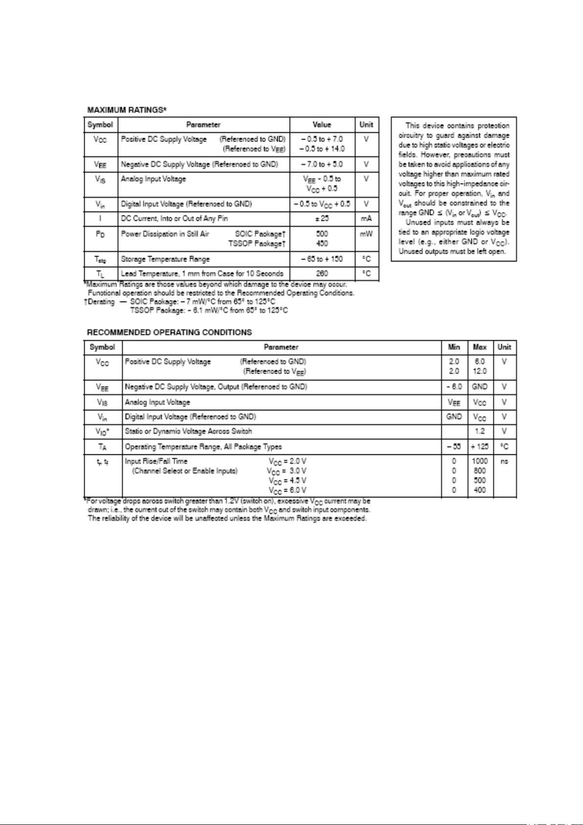
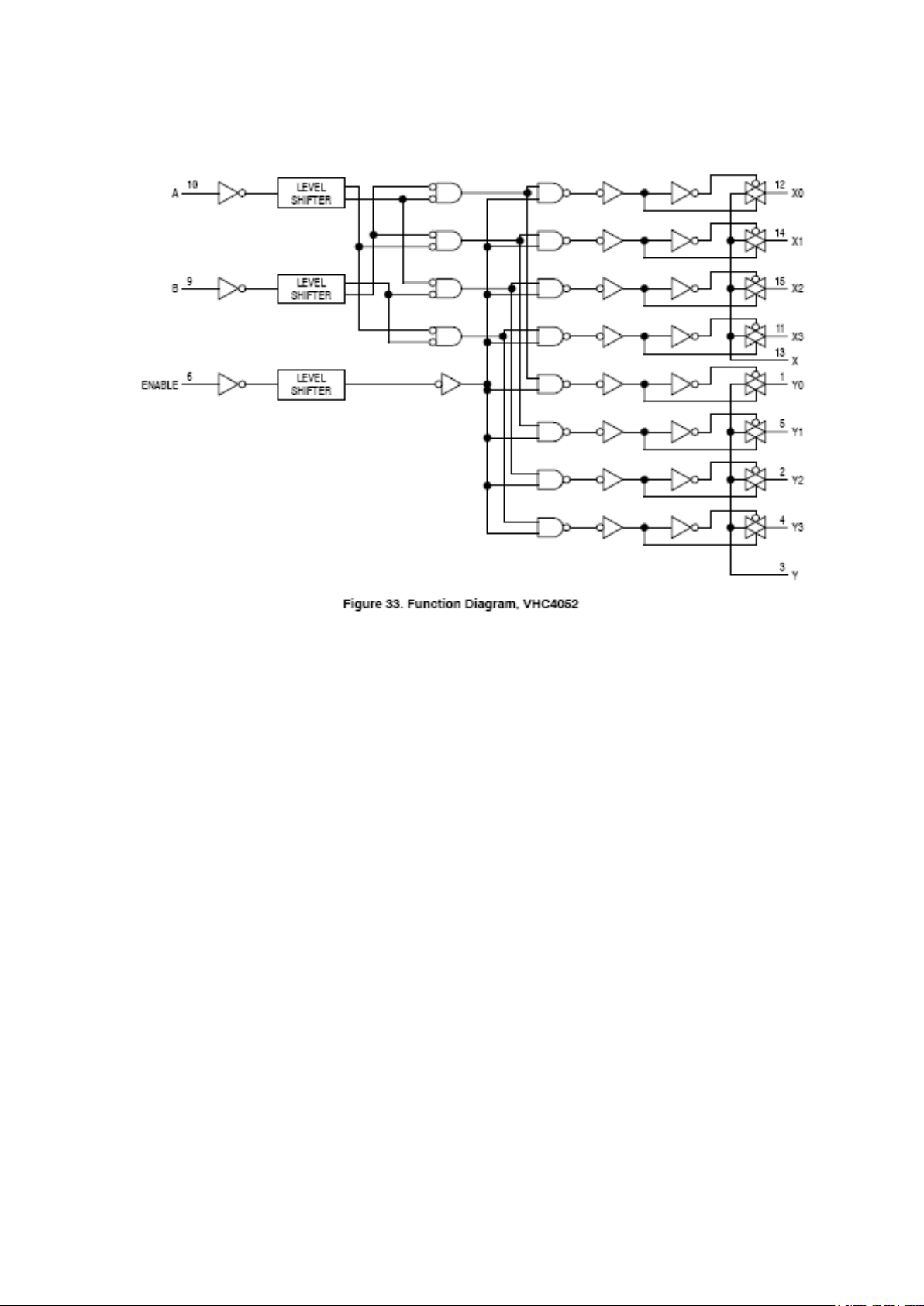
2.2.2.4. AV Switching
2.2.2.4.1. MC74VHC4052
The MC74VHC4052 utilize silicon--gate CMOS technology to achieve fast propagation delays,
low ON resistances, and low OFF leakage currents. These analog multiplexers/demultiplexers
control analog voltages that may vary across the complete power supply range (from VCC to
VEE).
The Channel--Select and Enable inputs are compatible with standard CMOS outputs; with pullup
resistors they are compatible with LSTTL outputs.
These devices have been designed so that the ON resistance (Ron) is more linear over input
voltage than Ron of metal--gate CMOS analog switches.
Fast Switching and Propagation Speeds
Low Crosstalk Between Switches
Diode Protection on All Inputs/Outputs
Analog Power Supply Range (VCC -- VEE) = 2.0 to 12.0 V
Digital (Control) Power Supply Range (VCC -- GND) = 2.0 to 6.0 V
Improved Linearity and Lower ON Resistance Than Metal—Gate Counterparts
Low Noise
2.2.2.4.2. NLAST4599
The NLAST4599 is an advanced high speed CMOS single pole − double throw analog switch
fabricated with silicon gate CMOS technology. It achieves high speed propagation delays and
low ON resistances while maintaining low power dissipation. This switch controls analog and
digital voltages that may vary across the full power
The device has been designed so the ON resistance (RON) is much lower and more linear over
input voltage than RON of typical CMOS analog switches.
The channel select input structure provides protection when voltages between 0 V and 5.5 V are
applied, regardless of the supply voltage. This input structure helps prevent device destruction
caused by supply voltage
− input/output voltage mismatch, battery backup, hot insertion, etc.
−supply range (from VCC to GND).
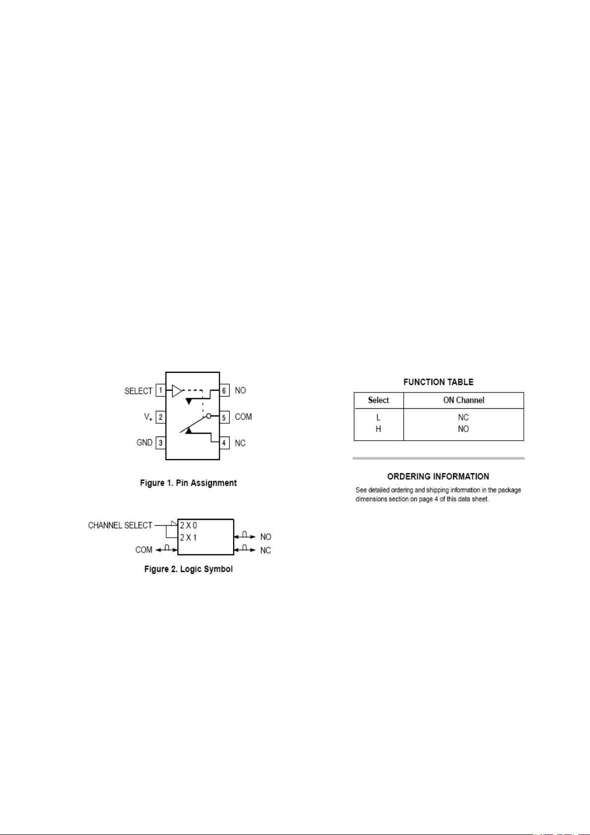
Features
Select Pin Compatible with TTL Levels
Channel Select Input Over−Voltage Tolerant to 5.5 V
Fast Switching and Propagation Speeds
Break−Before−Make Circuitry
Low Power Dissipation: ICC = 2 _A (Max) at TA = 25°C
Diode Protection Provided on Channel Select Input
Improved Linearity and Lower ON Resistance over Input Voltage
Latch−up Performance Exceeds 300 mA
ESD Performance: HBM > 2000 V; MM > 200 V
Chip Complexity: 38 FETs
Pb−Free Packages are Available
2.2.2.5. TUNER
Channel coverage of PLLTuner for VHF/UHF
OFF-AIR CHANNELS CABLE CHANNELS
BAND
CHANNELS
FREQUENCY
RANGE (MHz) CHANNELS
FREQUENCY
RANGE (MHz)
Low Band E2 to C 48.25 to 82.25 (1) S01 to S08 69.25 to 154.25
Mid Band E5 to E12 175.25 to 224.25 S09 to S38 161.25 to 439.25
High Band E21 to E69 471.25 to 855.25 (2) S39 to S41 447.25 to 463.25
(1). Enough margin is available to tune down to 45.25 MHz.
(2). Enough margin is available to tune up to 863.25 MHz.
Noise Typical Max. Gain Min. Typical Max.
Low band : 5dB 9dB All channels : 38dB 44dB 52dB
Mid band : 5dB 9dB Gain Taper (of-air channels): 8dB
High band : 6dB 9dB
Noise is typically 6dB for all channels. Gain is minimum 38dB and maximum 50dB for all
channels.
 Loading...