


TABLE OF CONTENTS
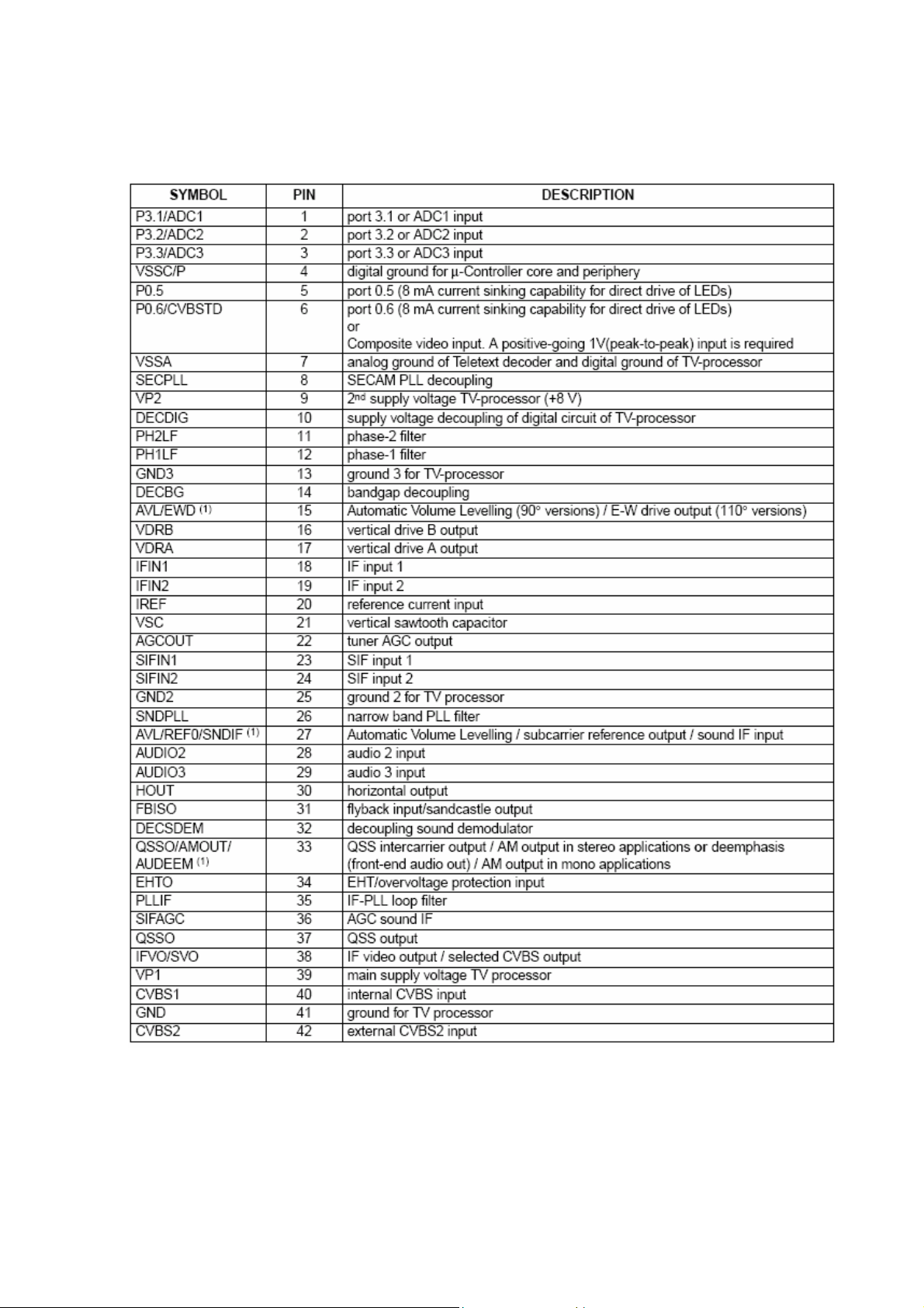
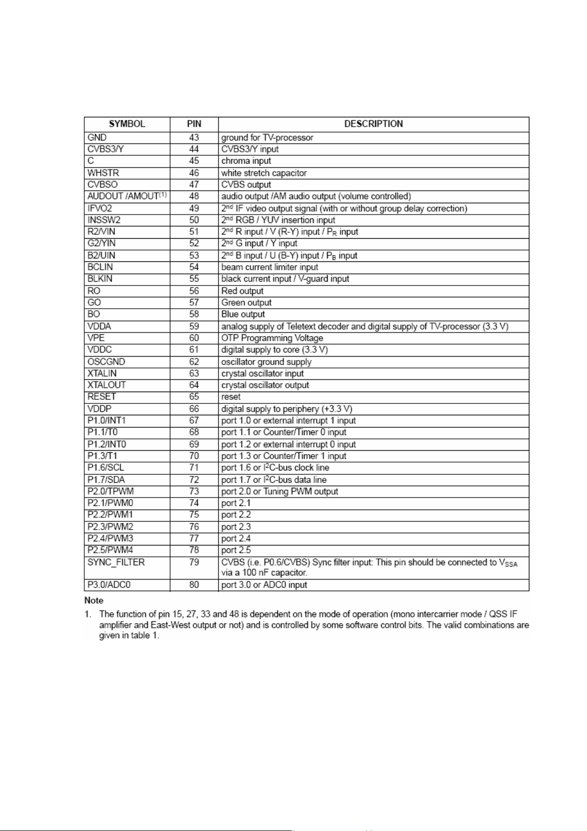
1. INTRODUCTION.....................................................................................................4
1.1. Purpose ....................................................................................................................................4
1.2. Scope .......................................................................................................................................4
1.3. General Features .......................................................................................................................4
2. GENERAL DESCRIPTION .......................... .. .. .. .. ... .. .. .. .. .. ... .. .. .. .. .. ... .. .. .. .. ... .. .. .. .....5
2.1. Introduction ..............................................................................................................................5
2.2. System Building Blocks...............................................................................................................5
2.2.1. AK57 Chassis Block Diagrams 5
2.2.1.1. Genaral...................................................................................................................5
2.2.1.2. SMPS ......................................................................................................................6
2.2.1.3. DEFLECTION ...........................................................................................................6
2.2.2. AK57 Chassis Main Blocks 7
2.2.2.1. UOC-II (ULTIMATE-ONE-CHIP).................................................................................8
2.2.2.2. Audio ....................................................................................................................16
2.2.2.3. External AV I/O .....................................................................................................18
2.2.2.4. AV Switching .........................................................................................................19
2.2.2.4.1. MC74VHC4052 ..................................................................................................19
2.2.2.4.2. NLAST4599 .......................................................................................................21
2.2.2.5. TUNER..................................................................................................................23
2.2.2.6. SAW FILTERS........................................................................................................25
2.2.2.6.1. K3958M (IF Filter for Video Applications).............................................................25
2.2.2.6.2. K9656M (IF Filter for Audio Applications) ............................................................25
2.2.2.6.3. K2966 (IF Filter for Intercarrier Applications).......................................................26
2.2.2.6.4. K2962 (IF Filter for Intercarrier Applications).......................................................26
2.2.2.6.5. G1975 (IF Filter for Intercarrier Applications) ......................................................27
2.2.2.7. SMPS ....................................................................................................................27
2.2.2.7.1. PRIMARY BLOCK ...............................................................................................27
2.2.2.7.1.1. SMPS CONTROLLER (NCP1207)..........................................................................28
2.2.2.7.1.2. MOSFET............................................................................................................31
2.2.2.7.1.2.1. MTP3N60E ......................................................................................................31
2.2.2.7.1.2.2. MTP6N60E ......................................................................................................32
2.2.2.7.2. SECONDARY BLOCK...........................................................................................33
2.2.2.7.3. SMPS Block Diagram..........................................................................................33
2.2.2.8. DEFLECTION .........................................................................................................34
2.2.2.8.1. HORIZANTAL DEFLECTION ................................................................................34
2.2.2.8.2. MD1803DFX ......................................................................................................34
2.2.2.8.3. FBT...................................................................................................................36
2.2.2.8.4. AN15524A (VERTICAL DEFLECTION OUTPUT).....................................................37
2.2.2.9. CRT BOARD ..........................................................................................................39
2.2.3. AK57 Chassis Scematics 42
2.2.3.1. Part1 ....................................................................................................................42
2.2.3.2. Part2 ....................................................................................................................43
2.2.3.3. Part3 ....................................................................................................................44
2.2.3.4. Part4 ....................................................................................................................45
2.2.4. DVD PLAYER 46
2.2.4.1. General Description ...............................................................................................46
2.2.4.1.1. MT1389D ..........................................................................................................46
2.2.4.1.2. SDRAM Memory Interface ..................................................................................46

2.2.4.1.3. Drive Interfaces.................................................................................................47
2.2.4.2. System Block Diagram and MT1389D Pin Description...............................................47
2.2.4.2.1. MT1389D Pin Description ...................................................................................47
2.2.4.2.2. 2.1 Sytem Block Diagram ...................................................................................56
2.2.4.3. Audio Output.........................................................................................................57
2.2.4.4. Audio DACS...........................................................................................................57
2.2.4.5. Video Interface......................................................................................................57
2.2.4.6. Flash Memory........................................................................................................58
2.2.4.7. Serial Eeprom Memory ...........................................................................................58
2.2.4.8. Audio Interface Audio Sampling Rate and PLL Component Configuration...................58
2.2.4.9. Scematics..............................................................................................................58
2.2.4.9.1. Part1 ................................................................................................................58
2.2.4.9.2. Part2 ................................................................................................................59
2.2.4.9.3. Part3 ................................................................................................................60
2.2.4.9.4. Part4 ................................................................................................................61
2.2.4.9.5. Part 5 ...............................................................................................................62
2.3. AK57 Service Menu..................................................................................................................64
2.4. TUNER SETTINGS....................................................................................................................75

1. Introduction
1.1. Purpose
This document is prepared for the UOCII TV project and describes the whole system features
and operating principles to be used in hardware design phase.
The document is based on “Device Specification UOCII-Version 1.12” from Philips
Semiconductors.
Prior to hardware design start, all parties involved must agree with the contents of this
document.
1.2. Scope
The document covers detailed descriptions of 11AK56 chassis system building blocks.
1.3. General Features
11AK57 is a 90° / 50 Hz. chassis which is capable of driving 14” superflat and 15” realflat CRT’s .
The chassis will have the following main features;
• Remote Control
• 100 programs
• On Screen Display
• Mono
• Colour Standarts ; PAL, SECAM, NTSC,
• Transmission standarts ; B/G, L/L’ I/I’, DK,
• Teletext ; One pages,
• Multi-standard alignment free PLL tuning,
• DVD or DVIX Player
• DVB-T option
• Europe Scart
• Detachable headphone output option,
• Front or side or back AV input option,
• Back AV output option,
• Coaxial output for IDTV/DVB-T
• 2W (%10 THD),
• 90-270V 50Hz or 170V-270V 50Hz SMPS
• Less than 3W
• DVD-Video, DVD R/RW, CD-R/RW, CD-Audio and MP3 Audio, JPEG (Picture CD), Video CD
and its sub formats like CVD, SVCD, DVCD.
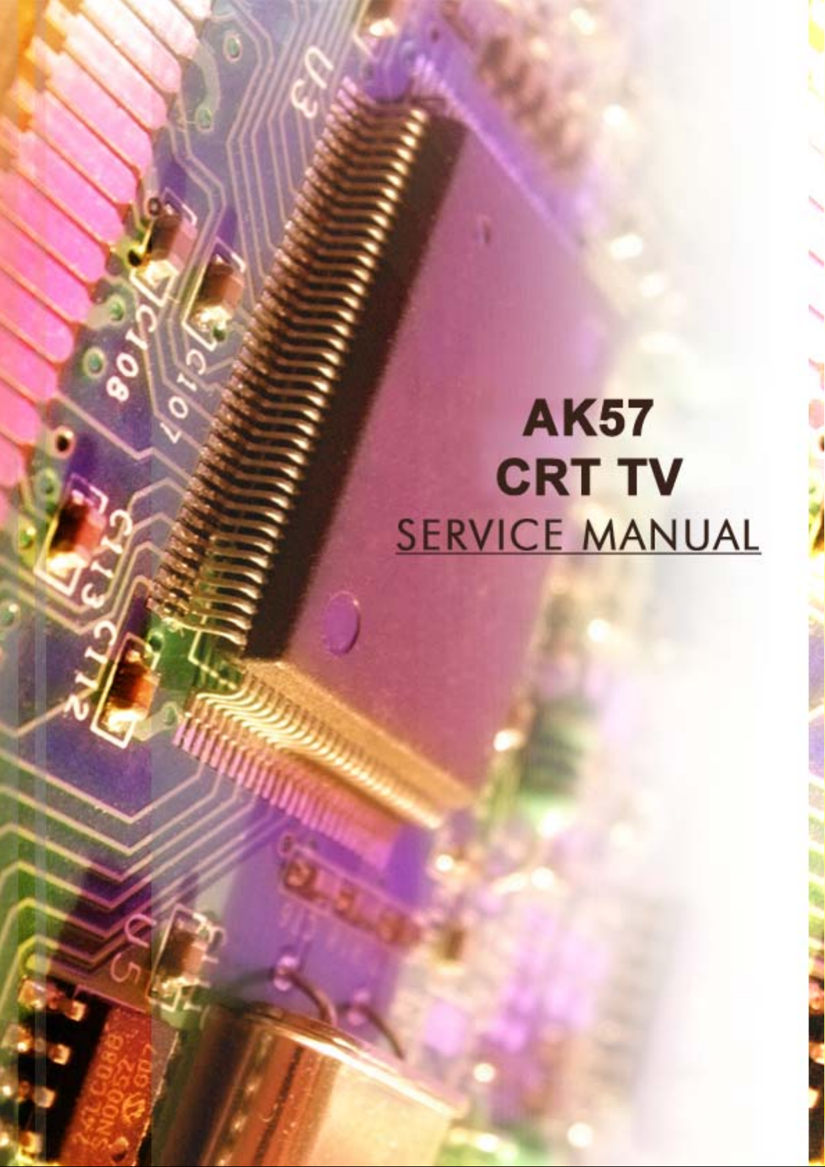
2. General Description
2.1. Introduction
This chapter describes system building blocks and their detailed descriptions.
2.2. System Building Blocks
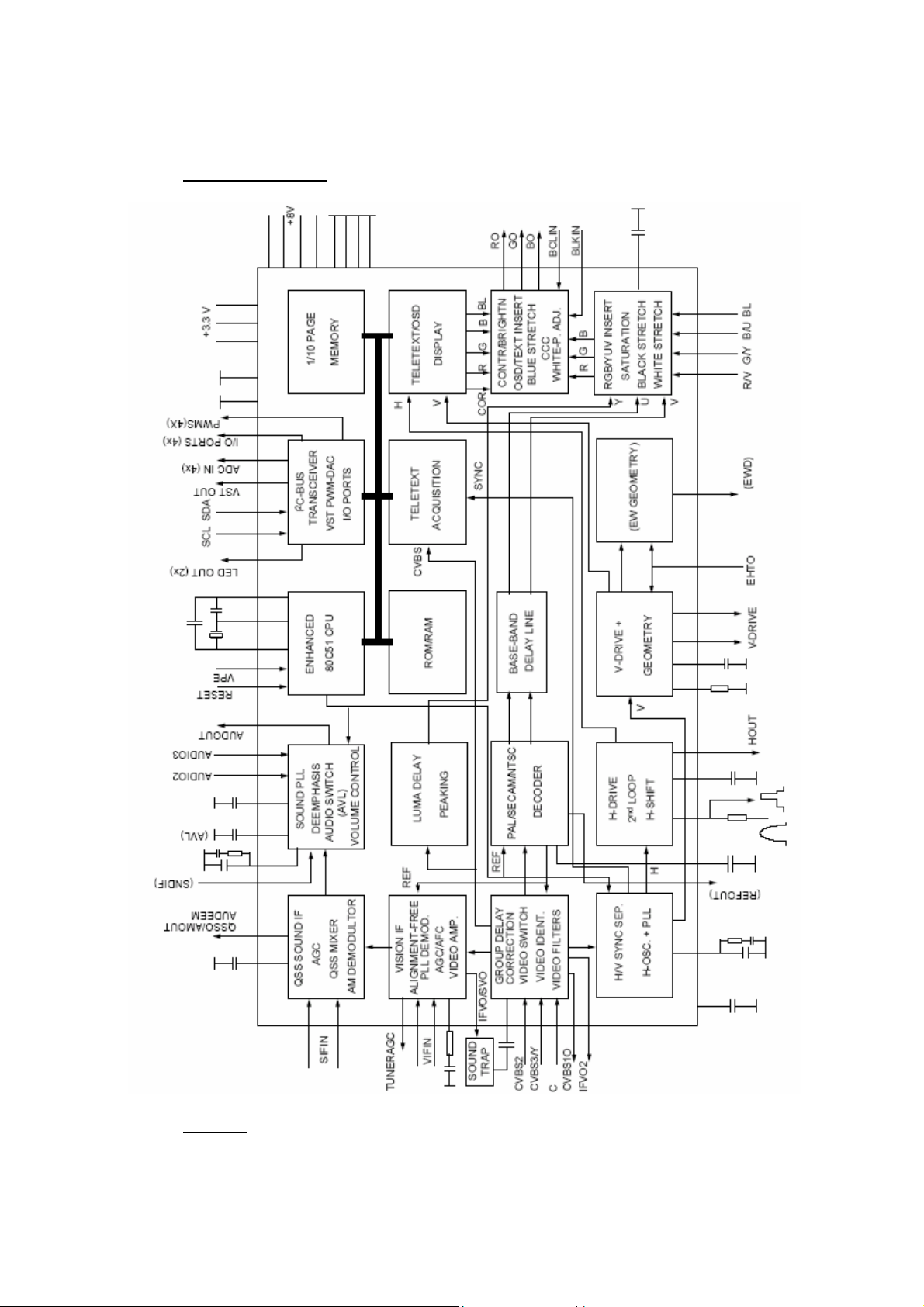
2.2.1. AK57 Chassis Block Diagrams
2.2.1.1. Genaral
DVD12V
DVB-T
RCA IN
SPDIF
IDTV30V
DVD5V
DVD
IDTV12V
Scart1
DVD3V3
DVD-IR
SPDIF-OUT
DVD-ON
DVD-MONO
DVD-CVBS
DVD-SPDIF
IDTV-CVBS
IDTV-MONO
IDTV-SPDIF
Rx
Tx
IRQ
RCA-CVBS-IN
RCA-MONO-IN
SC-PIN8
RGB-FB
SC-R
SC-G
SC-B
SC-CVBS-IN
SC-MONO-IN
SC-CVBS-OUT
SC-MONO-OUT
NLAST4599
75
SW0
SW1
SW0
V1
V2
VOUT
V3
V4
A1
A2
AOUT
A3
A4
4052
NLAST4599
P2.2_PWM1
76
P2.3_PWM2
80
P0.3_ADC0
42
CVBS2
28
AUDIO2
33
AUDEEM
77
P2.4_PWM3
SW2
69
P1.2_INT0
70
P1.3_T1
74
P2.1_PWM0
UOCII
P3.2_ADC2
50
51
2
P3.3_ADC3
CVBS1O
P1.1_T0
P0.5
52
53
47
68
5
STB
LED
NC
73
P2.0_PWM0
AUDOUT1
P2.5_PWM4
P3.1_ADC1
P1.0_INT1
9,39
67
3
1
KEYBOARD
TV-IR
8V
P0.6
59,61,66
3V3STB
71,72
18,19,
23,24
6
22
16,17
30
31
56,57,58
55
48
78
SECAM
PORT
MUTE
WP
IF
MONO
I2C
IF
BLOCK
AGC
VERTICAL DRIVE
HORIZANTAL DRIVE
EEPROM
TUN-IF
MUTE
HOR. FB
RGB
BLKIN
5VSTB
TUNER
5V
33V
2822M
A12V
12V
33V
B+
5V
8V
DEFLECTION
HEATER
V+
CRT BOARD
B+
12V
DVD12V
IDTV12
A12V
DVD5V
5VSTB
3V3STB
DVD3V3
STB
IDTV30V
EHT
RGB
SMPS
RCA-CVBS-OUT
RCA-MONO-OUT
11AK57
GENERAL BLOCK DIAGRAM
RCA OUT
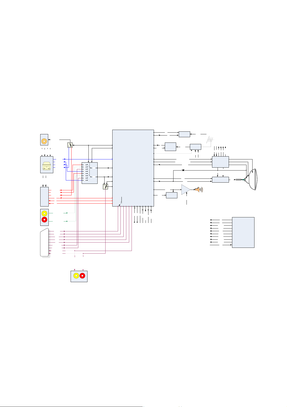
2.2.1.2. SMPS
1
2
3
4
DMAG
CONT_INT
NCP1207
I_SENSE
GND
220V
50Hz
8
VI
6
VCC
5
DRIVER
5
2
8
7
15
16
13
14
12
11
10
9
STB
B+
A12V
V
9
V
6
TR.REG
TR.REG
LDO
LDO
3V3STB
5VSTB
DVD3V3
DVD5V
SMPS BLOCK DIAGRAM
IDTV12V
DVD12V
12V
11AK57
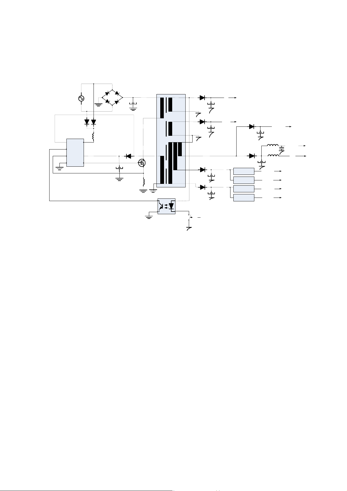
2.2.1.3. DEFLECTION
HORIZONTAL
DRIVE
HORIZONTAL
Lin.
Horz.
Yoke
30KV
FOCUS
SCREEN
+33V
+8V
+5V
-14V VERTICAL
+14V VERTICAL
RGB
DRIVE
+9V
VERTICAL
DRIVE
TRANSISTORS
CRT
BOARD
VERTICAL
AMPLIFIER
AN5524A
Heater
Heater
G2 FOCUS
VERTICAL
YOKE
30KV
2.2.2. AK57 Chassis Main Blocks
AK57 chassis main blocks are;
• UOCII : Microcontroller + Video Proccessor + Sound Proccessor + IF + Teletext
• AUDIO : Audio Amp.,
• EXT. AV I/O : Scart , AV input, AV output,
• AV SWITCHING : 4052, 4599
• TUNER : PLL Tuner

• SAW FILTERS
• SMPS : SMPS Controller, SMT, Bridge Rect., Line Filters
• DEFLECTION : FBT, HOT, Vertical Amplifier, Line Driver,
• CRT BOARD : RGB Amp. with transistors,
2.2.2.1. UOC-II (ULTIMATE-ONE-CHIP)
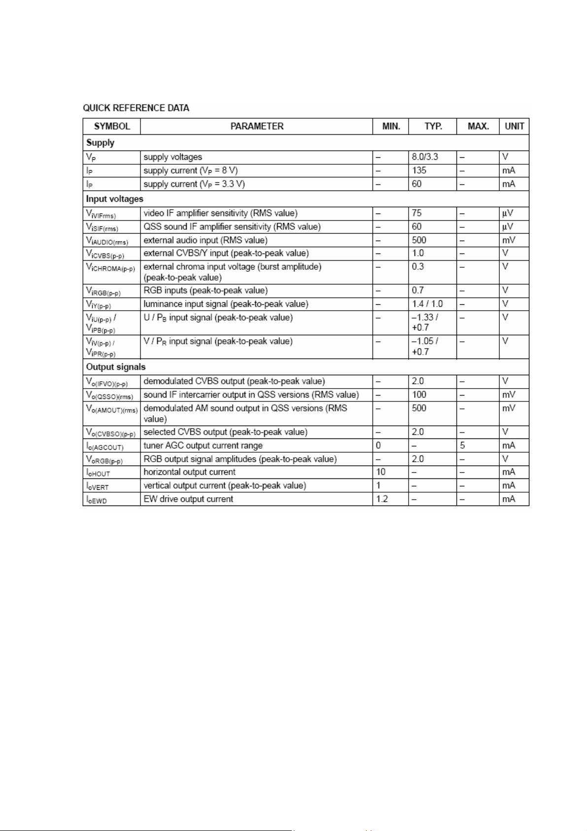
UOCII is composed of microcontroller, video proccessor, sound proccessor and IF blocks.
The various versions of the TDA955X H/N1 series combine the functions of a video processor
together with a microcontroller.The ICs are intended to be used in economy television receivers
with 90 and 110 degree picture tubes.
The ICs have supply voltages of 8V and 3.3V and they are mounted in a QFP 80 envelope.
The features are given in the following feature list.
FEATURES
TV-signal processor
• Multi-standard vision IF circuit with alignment-free PLL demodulator
• Internal (switchable) time-constant for the IF-AGC circuit
• The QSS and mono FM functionality are both available so that an FM/AM TV receiver can
be built without the use of additional ICs
• The mono intercarrier sound circuit has a selective
• FM-PLL demodulator which can be switched to the different FM sound frequencies
(4.5/5.5/6.0/6.5 MHz). The quality of this system is such that the external band-pass
filters can be omitted.
• The FM-PLL demodulator can be set to centre frequencies of 4.74/5.74 MHz so that a
second sound channel can be demodulated. In such an application it is necessary that an
external bandpass filter is inserted.
• The vision IF and mono intercarrier sound circuit can be used for the demodulation of
FM radio signals
• Video switch with 2 external CVBS inputs and a CVBS output. One of the CVBS inputs
can be used as Y/C input.
• 2 external audio inputs. The selection of the various inputs is coupled to the selection of
the CVBS signals
• Integrated chrominance trap circuit
• Integrated luminance delay line with adjustable delay time
• Switchable group delay correction in the CVBS path
• Picture improvement features with peaking (with switchable centre frequency,
depeaking, variable positive/negative overshoot ratio and video dependent coring),
dynamic skin tone control and blue-, black- and white stretching
• Integrated chroma band-pass filter with switchable centre frequency
• Switchable DC transfer ratio for the luminance signal
• Only one reference (12 MHz) crystal required for the m-Controller, Teletext- and the
colour decoder
• PAL/NTSC or multi-standard colour decoder with automatic search system

• Internal base-band delay line
• Indication of the Signal-to-Noise ratio of the incoming CVBS signal
• A linear RGB/YUV/YPBPR input with fast blanking for external RGB/YUV sources. The
synchronisation circuit can be connected to the incoming Y signal. The Text/OSD signals
are internally supplied from the
• m-Controller/Teletext decoder.
• RGB control circuit with ‘Continuous Cathode Calibration’, white point and black level off-
set adjustment so that the colour temperature of the dark and the light parts of the
screen can be chosen independently.
• Contrast reduction possibility during mixed-mode of OSD and Text signals
• Adjustable ‘wide blanking’ of the RGB outputs
• Horizontal synchronization with two control loops and alignment-free horizontal oscillator
• Vertical count-down circuit
• Vertical driver optimized for DC-coupled vertical output stages
• Horizontal and vertical geometry processing
• Horizontal and vertical zoom function for 16 : 9 applications
• Horizontal parallelogram and bow correction for large screen picture tubes
• Low-power start-up of the horizontal drive circuit
Microcontroller
• 80C51 m-controller core standard instruction set and timing
• 1 ms machine cycle
• 32 - 128Kx8-bit late programmed ROM
• 3 - 12Kx8-bit DataRAM (shared between Display, Acquisition and Auxiliary RAM)
• Interrupt controller for individual enable/disable with two level priority
• Two 16-bit Timer/Counter registers
• One 16-bit Timer with 8-bit Pre-scaler
• WatchDog timer
• Auxiliary RAM page pointer
• 16-bit Data pointer
• Stand-by, Idle and Power Down modes
• 14 bits PWM for Voltage Synthesis Tuning
• 8-bit A/D converter with 4 multiplexed inputs
•
5 PWM (6-bits) outputs for control of TV analogue signals
• 18 general I/O ports
Data Capture
• Text memory for 1 or 10 pages
• In the 10 page versions inventory of transmitted Teletext pages stored in the
Transmitted Page Table (TPT) and Subtitle Page Table (SPT)
• Data Capture for US Closed Caption
• Data Capture for 525/625 line WST, VPS (PDC system A) and Wide Screen Signalling
(WSS) bit decoding
• Automatic selection between 525 WST/625 WST
• Automatic selection between 625 WST/VPS on line 16 of VBI
• Real-time capture and decoding for WST Teletext in Hardware, to enable optimized m-
processor throughput

• Automatic detection of FASTEXT transmission
• Real-time packet 26 engine in Hardware for processing accented, G2 and G3 characters
• Signal quality detector for video and WST/VPS data types
• Comprehensive teletext language coverage
• Full Field and Vertical Blanking Interval (VBI) data capture of WST data
Display
• Teletext and Enhanced OSD modes
• Features of level 1.5 WST and US Close Caption
• Serial and Parallel Display Attributes
• Single/Double/Quadruple Width and Height for characters
• Scrolling of display region
• Variable flash rate controlled by software
• Enhanced display features including overlining, underlining and italics
• Soft colours using CLUT with 4096 colour palette
• Globally selectable scan lines per row (9/10/13/16) and character matrix [12x10, 12x13,
12x16 (VxH)]
• Fringing (Shadow) selectable from N-S-E-W direction
• Fringe colour selectable
• Meshing of defined area
• Contrast reduction of defined area
• Cursor
• Special Graphics Characters with two planes, allowing four colours per character
• 32 software redefinable On-Screen display characters
• 4 WST Character sets (G0/G2) in single device (e.g. Latin, Cyrillic, Greek, Arabic)
• G1 Mosaic graphics, Limited G3 Line drawing characters
• WST Character sets and Closed Caption Character set in single device
Optional Used ICs at AK57 chassis are TDA9550 H/N1, TDA9551 H/N1, TDA9552 H/N1.
FUNCTIONALOF TDA9550 H/N1
• TV range is 90°
• Mono intercarrier multi-standard sound demodulator (4.5 - 6.5 MHz) with switchable
centre frequency Audio switch
• Automatic Volume Levelling
• PAL decoder
• NTSC decoder
• ROM size 32 – 64K
• User RAM size 1K
• One page teletext
• Close Captioning
FUNCTIONALOF TDA9551H
•
TV range is 90°
• Mono intercarrier multi-standard sound demodulator (4.5 - 6.5 MHz) with switchable
centre frequency Audio switch

• Automatic Volume Levelling
• PAL decoder
• SECAM decoder
• NTSC decoder
• ROM size 32 – 64K
• User RAM size 1K
• One page teletext
• Close Captioning
FUNCTIONALOF TDA9552H
• TV range is 90°
• Mono intercarrier multi-standard sound demodulator (4.5 - 6.5 MHz) with switchable
centre frequency Audio switch
• Automatic Volume Levelling
• QSS sound IF amplifier with separate input and AGC circuit
• AM sound demodulator without extra reference circuit
• PAL decoder
• SECAM decoder
• NTSC decoder
• ROM size 32 – 64K
• User RAM size 1K
• One page teletext
• Close Captioning
BLOCK DIAGRAM
PINING
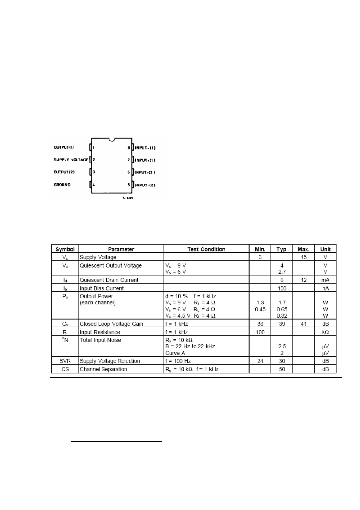
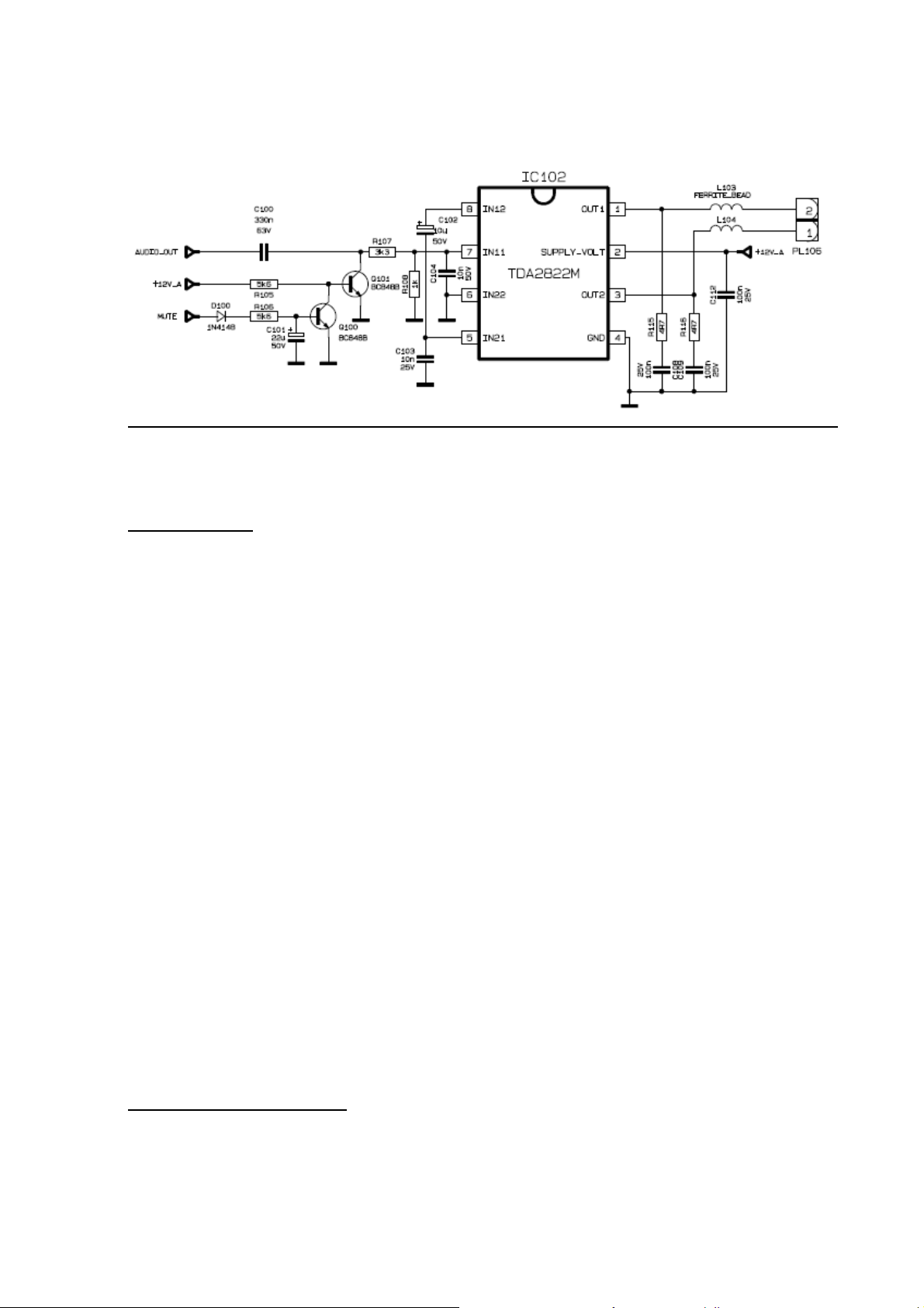
2.2.2.2. Audio
The TDA2822 is DUAL LOW-VOLTAGE POWER AMPLIFIER.
• Supply voltage down to 1.8V
• Low crossover distorsion
• Low quıescent current
• Bridge or stereo configuration
ELECTRICALCHARACTERISTICS
Figure: Test Circuit (Stereo)
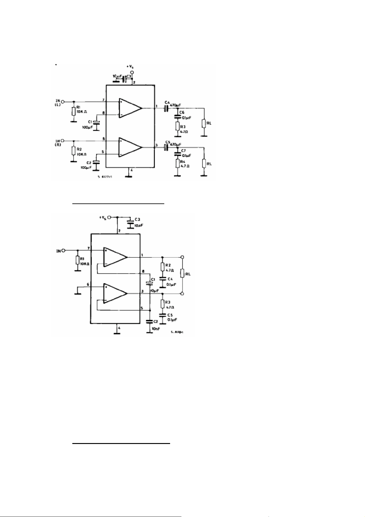
Figure: Test Circuit (Bridge)
Figure: Application in 11AK56
2.2.2.3. External AV I/O
SCART PINING
1. Audio right output 0.5Vrms / 1KΩ
2. Audio right input 0.5Vrms / 10K
3. Audio left output 0.5Vrms / 1K
4. Ground AF
5. Ground Blue
6. Audio left input 0.5Vrms / 10K
7. Blue input 0.7Vpp / 75
8. AV switching input 0-12VDC /10K
9. Ground Green
10. Not Used
11. Green input 0.7Vpp / 75
12. Not Used
13. Ground Red
14. Ground Blanking
15. Red input 0.7Vpp / 75
16. Blanking input 0-0.4VDC, 1-3VDC / 75
17. Ground CVBS output
18. Ground CVBS input
19. CVBS output 1Vpp / 75
20. CVBS input 1Vpp / 75
21. Ground
Front/Side/Back AV Input
Ω
Ω
Ω
Ω
Ω
Ω
Ω
Ω
Ω
Ω
Audio 0.5Vrms / 10KΩ
Video 1Vpp / 75
Ω
Back AV Output
Audio 0.5Vrms / 1K
Video 1Vpp / 75
Ω
Ω
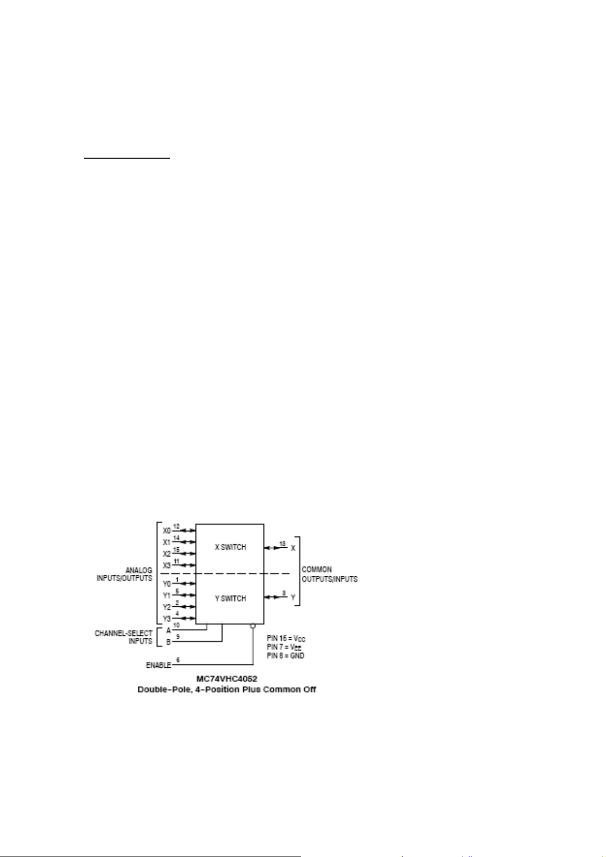
2.2.2.4. AV Switching
2.2.2.4.1. MC74VHC4052
The MC74VHC4052 utilize silicon--gate CMOS technology to achieve fast propagation delays,
low ON resistances, and low OFF leakage currents. These analog multiplexers/demultiplexers
control analog voltages that may vary across the complete power supply range (from VCC to
VEE).
The Channel--Select and Enable inputs are compatible with standard CMOS outputs; with pullup
resistors they are compatible with LSTTL outputs.
These devices have been designed so that the ON resistance (Ron) is more linear over input
voltage than Ron of metal--gate CMOS analog switches.
• Fast Switching and Propagation Speeds
• Low Crosstalk Between Switches
• Diode Protection on All Inputs/Outputs
• Analog Power Supply Range (VCC -- VEE) = 2.0 to 12.0 V
• Digital (Control) Power Supply Range (VCC -- GND) = 2.0 to 6.0 V
• Improved Linearity and Lower ON Resistance Than Metal—Gate Counterparts
• Low Noise
2.2.2.4.2. NLAST4599
The NLAST4599 is an advanced high speed CMOS single pole − double throw analog switch
fabricated with silicon gate CMOS technology. It achieves high speed propagation delays and
low ON resistances while maintaining low power dissipation. This switch controls analog and
digital voltages that may vary across the full power−supply range (from VCC to GND).
The device has been designed so the ON resistance (RON) is much lower and more linear over
input voltage than RON of typical CMOS analog switches.
The channel select input structure provides protection when voltages between 0 V and 5.5 V are
applied, regardless of the supply voltage. This input structure helps prevent device destruction
caused by supply voltage − input/output voltage mismatch, battery backup, hot insertion, etc.
Features
• Select Pin Compatible with TTL Levels
• Channel Select Input Over−Voltage Tolerant to 5.5 V
• Fast Switching and Propagation Speeds
• Break−Before−Make Circuitry
• Low Power Dissipation: ICC = 2 _A (Max) at TA = 25°C
• Diode Protection Provided on Channel Select Input
• Improved Linearity and Lower ON Resistance over Input Voltage
• Latch−up Performance Exceeds 300 mA
• ESD Performance: HBM > 2000 V; MM > 200 V
• Chip Complexity: 38 FETs
• Pb−Free Packages are Available
2.2.2.5. TUNER

Channel coverage of PLLTuner for VHF/UHF
OFF-AIR CHANNELS CABLE CHANNELS
BAND
CHANNELS
FREQUENCY
RANGE (MHz) CHANNELS
FREQUENCY
RANGE (MHz)
Low Band E2 to C 48.25 to 82.25 (1) S01 to S08 69.25 to 154.25
Mid Band E5 to E12 175.25 to 224.25 S09 to S38 161.25 to 439.25
High Band E21 to E69 471.25 to 855.25 (2) S39 to S41 447.2 5 to 463.25
(1). Enough margin is available to tune down to 45.25 MHz.
(2). Enough margin is available to tune up to 863.25 MHz.
Noise Typical Max. Gain Min. Typical Max.
Low band : 5dB 9dB All channels : 38dB 44dB 52dB
Mid band : 5dB 9dB Gain Taper (of-air channels): 8dB
High band : 6dB 9dB
Noise is typically 6dB for all channels. Gain is minimum 38dB and maximum 50dB for all
channels.
Terminals for External Connection
Electrical cond itions

2.2.2.6. SAW FILTERS
2.2.2.6.1. K3958M (IF Filter for Video Applications)
Standard
• B/G
• D/K
• I
• L/L’
Pin configuration
1 Input
2 Input - ground
3 Chip carrier - ground
4 Output
5 Output
Features
• TV IF video filter with Nyquist slopes at 33.90 MHz and 38.90 MHz
• Constant group delay
2.2.2.6.2. K9656M (IF Filter for Audio Applications)
Standard
• B/G
• D/K
• I
• L/L’
Pin configuration

1 Input
2 Input - ground
3 Chip carrier - ground
4 Output
5 Output
Features
• TV IF audio filter with two channels
• Channel 1 (L’) with one pass band for sound carriers at 40,40 MHz (L’) and 39,75 MHz
(L’- NICAM)
• Channel 2 (B/G, D/K, L, I) with one pass band for sound carriers between 32,35 MHz
and 33,40 MHz
2.2.2.6.3. K2966 (IF Filter for Intercarrier Applications)
Standard
• B/G
• D/K
Pin configuration
1 Input
2 Input - ground
3 Chip carrier - ground
4 Output
5 Output
Features
• TV IF filter with Nyquist slope and sound shelf
• Broad sound shelf for sound carriers at 32,40MHz and 33,40 MHz
• Group delay predistortion
2.2.2.6.4. K2962 (IF Filter for Intercarrier Applications)
Standard
• B/G
• I
• L/L’
Pin configuration
1 Input
2 Input - ground
3 Chip carrier - ground
4 Output
5 Output

Features
• TV IF filter with two Nyquist slope and sound shelf
• Picture carriers at 33,90 MHz and 38,90 MHz
• Broad sound shelf at 15 dB level for sound carriers at 32,90 MHz and 33,40 MHz
• Constant group delay
2.2.2.6.5. G1975 (IF Filter for Intercarrier Applications)
Standard
• B/G
Pin configuration
1 Input
2 Input - ground
3 Chip carrier - ground
4 Output
5 Output
Features
• TV IF filter with Nyquist slope and sound shelf
• Picture carrier at 38.90MHz
• Reduced group delay predistortion as compared with standard B/G, half
2.2.2.7. SMPS
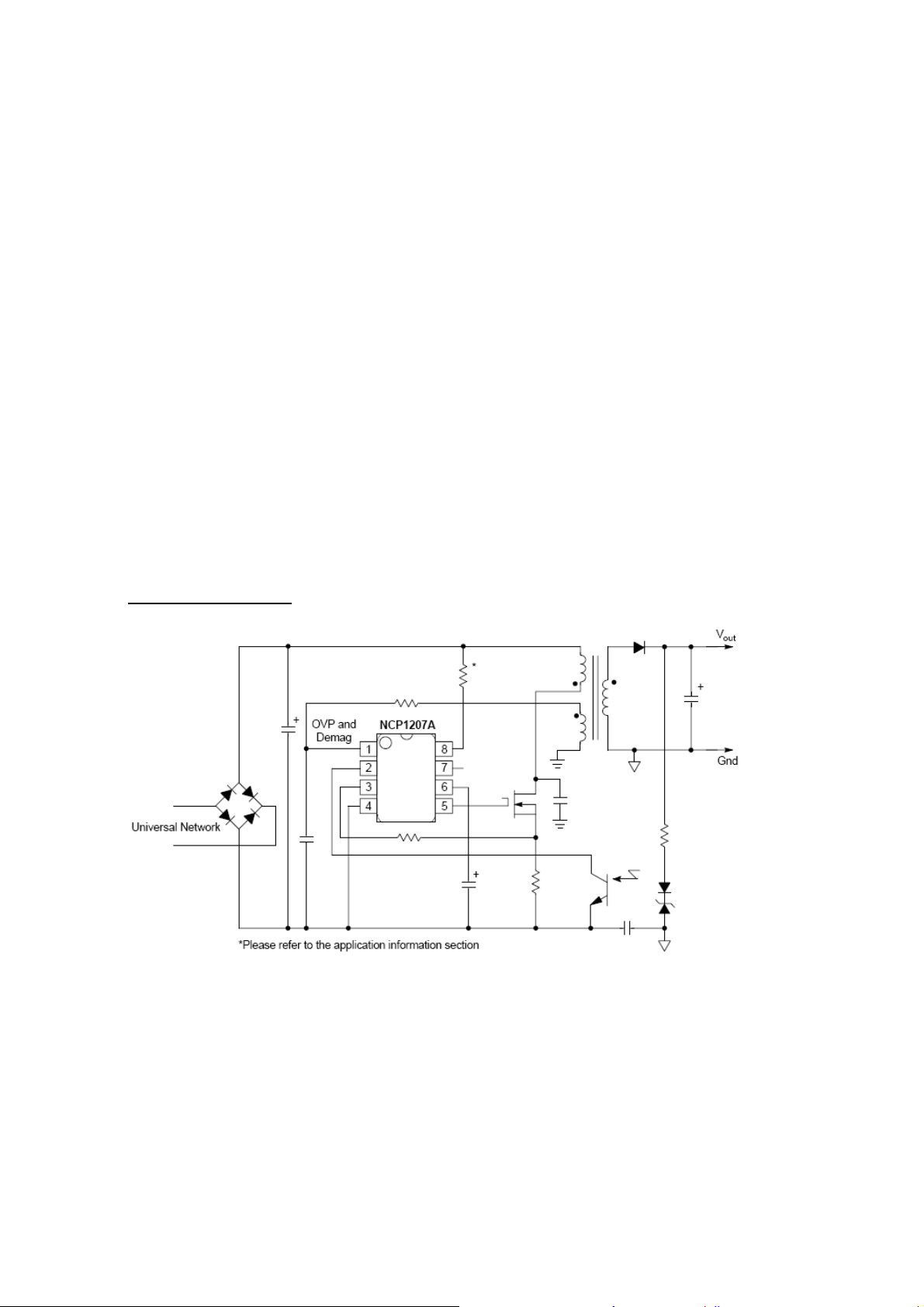
2.2.2.7.1. PRIMARY BLOCK
AC power applied via AC inlet, line filter components prevent chassis from incoming noise of AC
line, also prevents AC line against created noises by TV. Bridge rectifier and bulk capacitor
converts AC voltage to DC voltage. Applied DC voltage to primary winding is then swicthed via
MOSFET by primary controller in a controlled manner.
SMPS controller works on quasi-resonant PWM and gets first supply voltage from AC line (SMPS
Controller supply). Controller drives MOSFET according to feedback information supplied by
shunt regulator and opto-coupler, according to that information adjusts on-time of MOSFET for
required power. After the start-up in normal operation mode SMPS controller is supplied by SMT.
Primary block consist of following main parts,
AC Inlet (PL800),
Fuse (F800),
Varistor (R803),

Line Filter For EMC (C801,L800,C800),
SMPS Controller (IC806),
SMPS Controller supply for first Start-up (R807),
Bridge Rectifier (D820,D821,D822,D823),
Rectifier For SMPS Controller(D803),
Bulk Cap (C809),
Clamping Circuitry (R820, C810, C811, D824),
SMT (Switch Mode Transformer) (TR800),
SMT Driver MOSFET (Q802),
Current Sense Resistor (R828),
Protection Components for MOSFET Failure (D805,D806,R826)
2.2.2.7.1.1. SMPS CONTROLLER (NCP1207)
PWM Current-Mode Controller for Free Running Quasi-Resonant Operation
The NCP1207A combines a true current mode modulator and a demagnetization detector to
ensure full borderline/critical Conduction Mode in any load/line conditions and minimum drain
voltage switching (Quasi−Resonant operation). Due to its inherent skip cycle capability, the
controller enters burst mode as soon as the power demand falls below a predetermined level. As
this happens at low peak current, no audible noise can be heard. An internal 8.0 _s timer
prevents the free−run frequency to exceed 100 kHz (therefore below the 150 kHz CISPR−22
EMI starting limit), while the skip adjustment capability lets the user select the frequency at
which the burst foldback takes place.
The Dynamic Self−Supply (DSS) drastically simplifies the transformer design in avoiding the use
of an auxiliary winding to supply the NCP1207A. This feature is particularly useful in applications
where the output voltage varies during operation (e.g. battery chargers). Due to its
high−voltage technology, the IC is directly connected to the high−voltage DC rail. As a result,
the short−circuit trip point is not dependent upon any VCC auxiliary level.
The transformer core reset detection is done through an auxiliary winding which, brought via a
dedicated pin, also enables fast Overvoltage Protection (OVP). Once an OVP has been detected,
the IC permanently latches off.
Finally, the continuous feedback signal monitoring implemented with an overcurrent fault
protection circuitry (OCP) makes the final design rugged and reliable.
Features
• Free−Running Borderline/Critical Mode Quasi−Resonant Operation
• Current−Mode with Adjustable Skip−Cycle Capability
• No Auxiliary Winding VCC Operation
• Auto−Recovery Overcurrent Protection
• Latching Overvoltage Protection
• External Latch Triggering, e.g. Via Overtemperature Signal
• 500 mA Peak Current Source/Sink Capability
• Undervoltage Lockout for VCC Below 10 V
• Internal 1.0 ms Soft−Start
• Internal 8.0 _s Minimum TOFF
• Adjustable Skip Level
• Internal Temperature Shutdown
• Direct Optocoupler Connection
• SPICE Models Available for TRANsient Analysis
• Pb−Free Package is Available Typical Applications
• AC/DC Adapters for Notebooks, etc.
• Offline Battery Chargers
• Consumer Electronics (DVD Players, Set−Top Boxes, TVs, etc.)
• Auxiliary Power Supplies (USB, Appliances, TVs, etc.)
Typical Application:
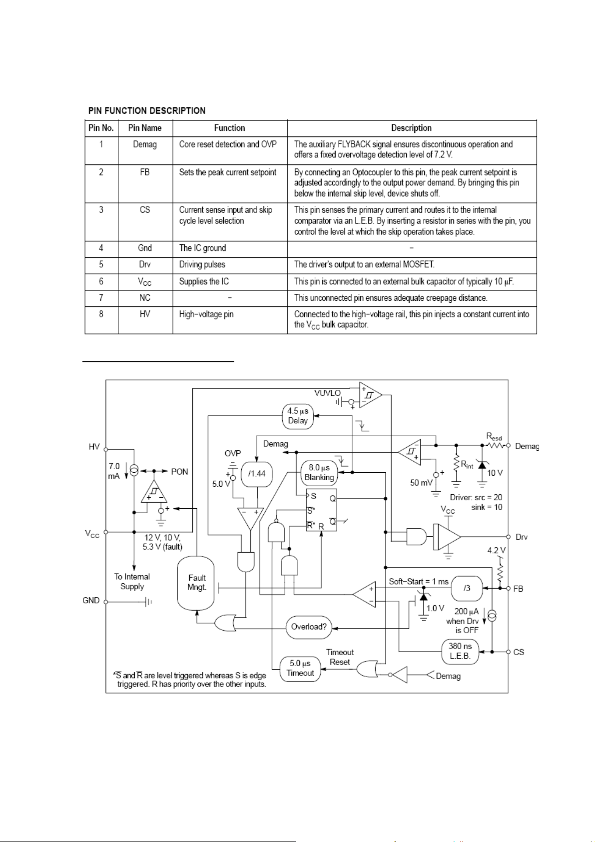
Internal Circuit Architecture

2.2.2.7.1.2. MOSFET
The MTP3N60E used for voltage range 170-270V, The MTP6N60E used for voltage range 90 –
270V.
2.2.2.7.1.2.1. MTP3N60E
N–Channel Enhancement–Mode Silicon Gate
This advanced high voltage TMOS E–FET is designed to with stand high energy in the
avalanche mode and switch efficiently. This new high energy device also offers a drain–to–
source diode with fast recovery time. Designed for high voltage, high speed switching
applications such as power supplies, PWM motor controls and other inductive loads, the
avalanche energy capability is specified to eliminate the guesswork in designs where inductive
loads are switched and offer additional safety margin against unexpected voltage transients.
Avalanche Energy Capability Specified at Elevated Temperature
Low Stored Gate Charge for Efficient Switching
Internal Source–to–Drain Diode Designed to Replace External Zener Transie nt Suppressor —
Absorbs High Energy in the Avalanche Mode
Source–to–Drain Diode Recovery Time Comparable to Discrete Fast Recovery Diode
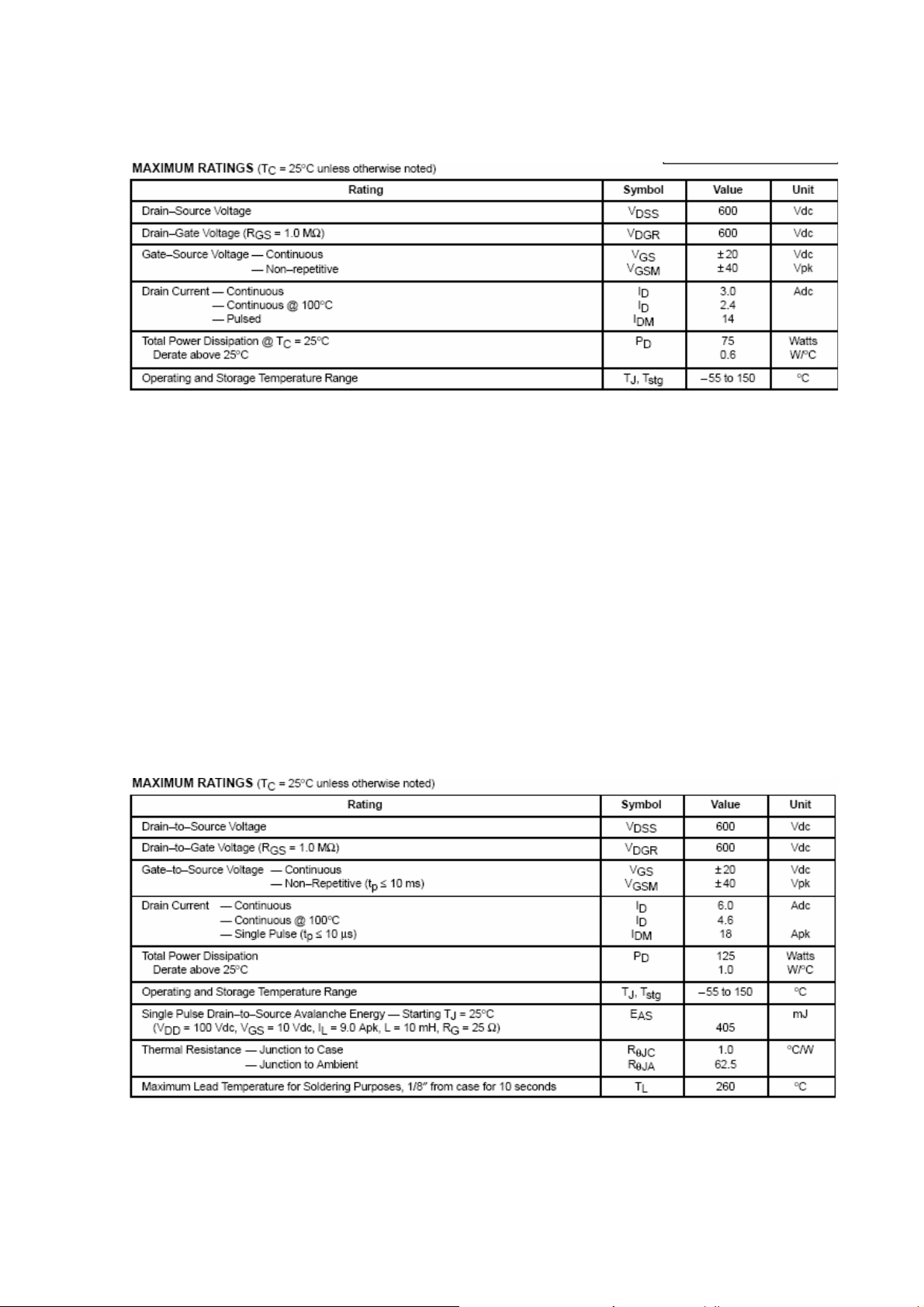
2.2.2.7.1.2.2. MTP6N60E
N–Channel Enhancement–Mode Silicon Gate
This high voltage MOSFET uses an advanced termination scheme to provide enhanced
voltage–blocking capability without degrading performance over time. In addition, this advanced
TMOS E–FET is designed to withstand high energy in the avalanche and commutation modes.
The new energy efficient design also offers a drain–to–source diode with a fas t recovery time.
Designed for high voltage, high speed switching applications in power supplies, converters and
PWM motor controls, these devices are particularly well suited for bridge circuits where diode
speed and commutating safe operating areas are critical and offer additional safety margin
against unexpected voltage transients
.
• Robust High Voltage Termination
• Avalanche Energy Specified
• Source–to–Drain Diode Recovery Time Comparable to a Discrete Fast Recovery Diode
• Diode is Characterized for Use in Bridge Circuits
• IDSS and VDS(on) Specified at Elevated Temperature
2.2.2.7.2. SECONDARY BLOCK
Switching primary winding of SMT induces voltages to secondary windings of SMT. Induced
voltages are then rectified by secondary recitification diodes and capacitors.
Output Voltages
+3.3.V_STB : The signal is +3.3VDC and continuous stand-by on/off. Used for digital part of
UOCII.
+5V_STB : The signal is +5VDC and continuos stand-by on/off. Used for port control.
B+ : The voltage needed for FBT. Voltage range 114V – 117V according to CRT.
12V : The voltage needed for horizantal driver circuit.
12V_A : The voltage supply of audio amplifier.
12V_DVD : The voltage needed for DVD.
12V_IDTV : The voltage needed for IDTV.
+5V_DVD : The voltage needed for DVD.
+3.3.V_DVD : The voltage needed for DVD.
2.2.2.7.3. SMPS Block Diagram
220V
50Hz
1
2
3
4
DMAG
CONT_INT
I_SENSE
GND
NCP1207
DRIVER
8
VI
6
VCC
5
5
2
8
7
15
16
13
14
12
11
10
9
STB
B+
A12V
9
V
6
V
TR.REG
TR.REG
LDO
LDO
3V3STB
5VSTB
DVD3V3
DVD5V
SMPS BLOCK DIAGRAM
IDTV12V
DVD12V
12V
11AK57

2.2.2.8. DEFLECTION
2.2.2.8.1. HORIZANTAL DEFLECTION
Deflection block consist of following main parts,
Horizontal driver transistor (Q600),
Horizontal driver (L600),
HOT (Horizontal Output Transistor) (Q603),
FBT (TR600),
Linearity Coil (L601),
Flyback Capacitors (C611),
S-correction capacitor (C622),
Modulated S-correction capacitor (C623),
Hdrive signal is buffered and applied to line driver transistor by a capacitor.
Line driver produces necessary base currents, parallel diode to base series resistor speeds up
the reverse base current.
UOCII has soft-start and soft-stop features to have more safe operation. There are two base
current adjustment resistors on the circuit. Collector current differs according to CRT sizes .
Tube dependent components are choosen to fit best picture performance by keeping;
11-12usec. Flyback time,
Max. 1300V. collector voltage (peak-detect mode measurement)
2.2.2.8.2. MD1803DFX
HIGH VOLTAGE NPN POWER TRANSISTOR FOR STANDARD DEFINITION CRT DISPLAY
Features
• State-Of-The-Art Technology: – Diffused collector “ENHANCED GENERATION”
• More stable performance versus operating temperature variation
• Low base drive requirement
• Tighter hFE range at operating collector current
• Fully insulated power package U.L. compliant
• Integrated free wheeling diode
• In compliance eith the 2002/93/EC EUROPEAN DIRECTIVE

2.2.2.8.3. FBT
Operating Ampient Temperatue : -10°C..........+60°C
Stroge Ampient Temperature : -20°C..........+80°C
Operating Horizantal Frequency : 15.625KHz ±0.5KHz
INDUCTANCE (Between pin1 to pin3) : 3.02mH ± %8
INTERNAL RESISTANCE : Max. 2.2Ohm Regulation:Max.%10
FLYBACK TIME : 11.5µsec
COLLECTOR VOLTAGE : 1000Vp_p
FOCUS VOLTAGE RANGE % OF EHT: min.≤18.2 max.≥34.6
DEFLECTION CURRENT : 3.1Ap_p max.
AUXLIARY OUTPUTS:
Heater Voltage : 6.3Vrms / max 750mA
RGB Supply : +200V / max 30mA
Vertical Supply : +14V / max 1A ±%5
Vertical Supply : -14V / max 1A ±%5
Auxliary Voltage : +9V / max 1A ±%5
Tuning Voltage : +33V max 100mA
±%5
±%5

2.2.2.8.4. AN15524A (VERTICAL DEFLECTION OUTPUT)
The AN5524A (TV vertical deflection output circuit) is a monolithic integrated circuit designed for
vertical deflection output, such as TV and display.
Features
• Built-in Pump-up circuit
• Built-in Thermal protection circuit
• Maximum deflection current = 1. 6Ap-p
• Dimple forming type :
Advantages : a) Withstand repeated movements between the body and the solder joint of the IC
(when a heat-sink is used).
b) Better vibration absorber (eg. CTV installed in the bus/coach).
• VCC operating range : 12V ~ 30V

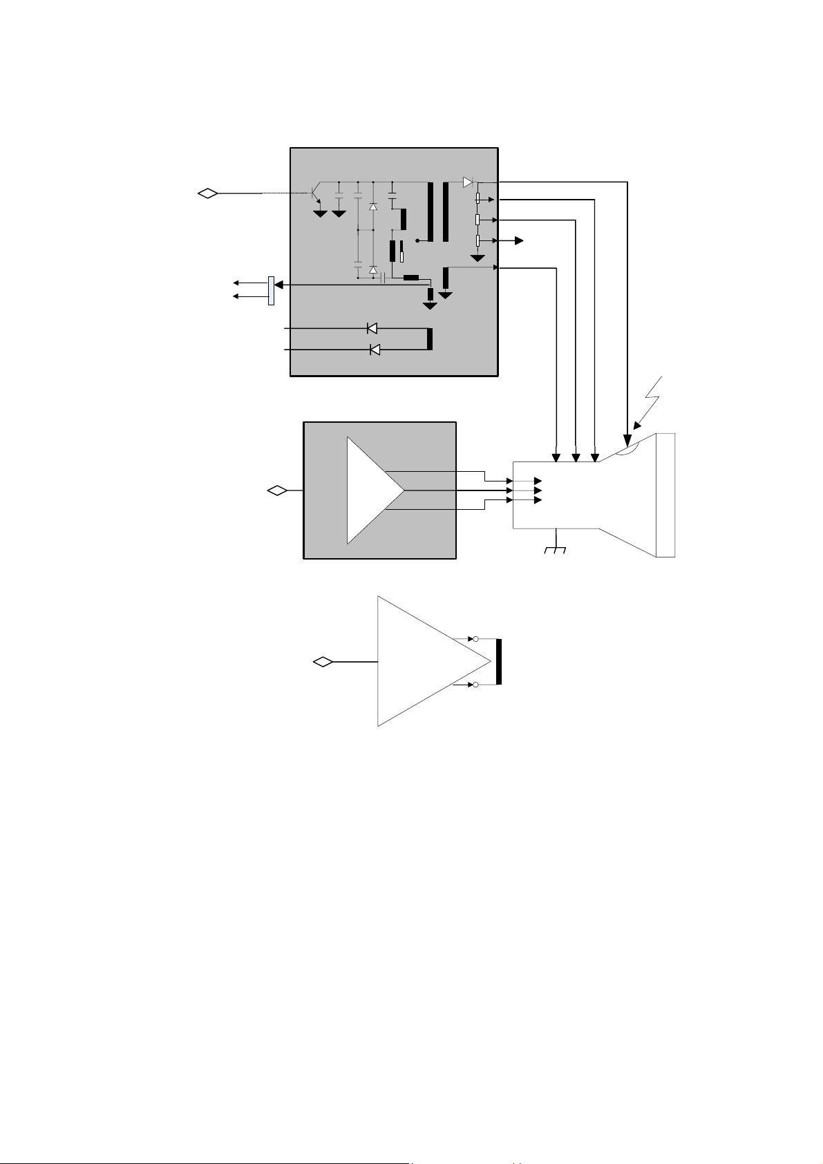
2.2.2.9. CRT BOARD
Transistors are used for amplifying RGB signals.
2SC2482 For High Voltage Switching And Amplifier Applications:
• High Voltage : V
• Small Collector Output Capacitance : C
(BR)=300V.
ob=3.0pF (typ.)


2.2.3. AK57 Chassis Scematics
2.2.3.1. Part1
AUDIO_OUT
MUTE
6
5
4
3
2
1
PL100
D100
1N4148
D121
C106
IF1 11
IF2/GND 10
VST 9
NC/ADC 8
VS 7
NC 6
TU100
SDA 5
38.9MHz_TVTUN
SCL 4
AS 3
VT 2
AGC 1
L125
BLM21A601S
D122
C108
D123
ESD_20V
10n
C107
22u
50V
ESD_20V
6n8
50V
R104
5k6
C102
100u
50V
R103
16V
C101
100n
50V
C100
C104
ESD_20V
C109
4u7
50V
5k6
C128
5
1N4148
15k
D107
100R
R176
53B2_UIN
12 PF1LF
15k
C154
100n
16V
100n
C145
C147
52G2_YIN
13 GND3
VPROT
16V100n
C148
51R2_VIN
14 DECBG
50V4u7
SC_B_IN
R177
16V100n
50INSSW2
15 AVL
C155
C156
2u2
50V
SC_G_IN
R178
470R
49IFVO2
16 VDRB
100R
R180
VERT+
SC_R_IN
SC_FBLK
CVBS_OUT
AUDIO_OUT
470R
R184
100R
47CVBS10
48AUDOUT1
17 VDRA
18 IFIN1
C161
C162
100R
R189
VERT-
R185
50V100n C157
100R
46WHSTR
19 IFIN2
50V1n5
50V1n5
R187
16V100n C158
20 IREF 45C
39k
COMMON
SEL_CVBS
100R
R186
16V
220n C159
43GNDA1
44CVBS3_Y
21 VSC
22 AGCOUT
C163
100n
63V
OUT1 4
IN11
2.2.3. AK57 Chassis Scematics
2.2.3.1. Part1
+8V
C168
C164
S101
C165
50V 10n
220n
16V
10n
50V
OPTIONAL
R188
75R
40CVBS1
39VP1
38SVO_IFOUT
37IC2
36SIFAGC
35PLLIF
34EHTO
33AUDEEM
32DECSDEM
31FBISO
30HOUT
29AUDIO3
28AUDIO2
27REFOUT_SNDIF
26SNDPLL
25GND2
R206
470R
C170
OUT1 4
IN11
1N4148
BA591
390R
R196
50V
R200
C180
D104
D105
L115
50V1uC169
4u7
2k2
C172
100n
R254
16V220nC177
16V220nC178
R201
R195
4R7
1u
C173
100u
R197
3
R208
1k
S102
R202
100R
R203
R204
R205
C171
27k
10k
820p
1k
Q116
100n
50V
16V
16V
C174
2n7
50V
BC848B
C175
10n
C181
10u
50V
50V
HFLYBACK
SEL_MONO
R209
R210
16V
1k
30k
C179
4n7
50V
OUT2 5
GND
IN22
1k
C160
Z100
42CVBS2
23 IC
K3958M
16V
220n
24 IC1 41GND
3
OUT2 5
GND
IN22
100R
R198
Q115
BC858B
C176
50V1u
SAW_SW
1k2
1k2
C186
270p
50V
R216
220R
27k
R199
L120
4.5MHz_TRAP
Z102
2k7
R224
HOUT
R217
100k
R218
120k
123
L118
6u8
123
AGC
C187
100n
4.5MHz_TRAP
Z103
680k
R219
470k
R225
L119
BLM21A601S
+5V
TV R&D GROUPVESTEL ELECTRONICS
001.sht
03
R223
100R
C193
47u
50V
Rev.
RCA_A_IN
RCA_V_IN
Ver.
820R
R220
R226
R215
220R
R221
+5V_STB
BC848B
Q118
180R
EHT_INFO
+8V
RF_MONO
R222
16V
6k2
Q119
BC848B
3k3
11AK57 VIDEO&AUDIO
DATE
08/10/2007 01 of 04
L122
DVD_CVBS
DVD_ON
IDTV_CVBS
IDTV_MONO 1k
DVD_MONO
DVD_SPDIF
IDTV_SPDIF
2u2
Author
YALCIN ELIK
D116
D117
ESD_20V
75R
R233
R241
ESD_20V
BLM21A601S
R242
100R
10k
R245
R247
R248
R243
10k
75R
10k
10k
L124
R246
R249
1k
R250
100R
R251
100R
R244
75R
PL111
PL112
Sheet
1
2
3
1
2
1
2
3
2
1
2
1
A
31245
BC
JK102
RACK_RCA_DVB
2
1
PL121
PL113
PL114
PL115
1
2
PL116
3
1
2
PL117
1
2
PL118
16V
BLM21A601S
D108
L104
R114
100R
R115
100R
PL108
BC858B
Q104
L103
+5V_STB
BLM21A601S
R147
100R
2
1
220p
50V
R123
R129
PL109
10k
Q105
BC848B
C130
SDA
10k
3
2
1
SCL
100n
1
2
3
100R
56RO
BC848B
Q111
55BLKIN
4
D103
R173
C146
390p
50V
54BCLIN
IC103
220R
330k
C136
C138
100u
16V
C139
100u
R159
BC858B
Q107
C135
47u
16V
C140
100n
X100
12MHz
16V
C141
100n
16V
63XTALIN
64XTALOUT
C142
47p
50V
16V
47p
50V
REMOTE
R124
100R
R126
330R
R125
330R
10k
R127
R128
100R
KEYBOARD
16V
D102
TX
RX
STBY
STBY_PR
S106
MUTE
IRQ
SW2
SW1
SW0
LED
REMOTE
R130
R157
100R
R156
100R
R155
100R
4k7
+5V_STB
4k7
R131
R138
+5V_STB
4k7
R139
+3V3_STB
BLM21A601S
10k
4k7
4k7
R141
R140
L109
+3V3_STB
C131
100u
16V
EHT_INFO
R154
100R
R148
100R
R142
100R
R143
100R
R144
100R
R145
100R
R146
100R
16V
C132
100n
R137
4k7
220k
R136
R158
L108
BLM21A601S
L110
BLM21A601S
65 RESET
66 VDDP
67 P1.0_INT1
68 P1.1_T0
69 P1.2_INTO
70 P1.3_T1
71 P1.6_SCL
72 P1.7_SDA
73 P2.0_PMW
74 P2.1_PWM0
75 P2.2_PWM1
76 P2.3_PWM2
77 P2.4_PWM3
78 P2.5_PWM4
61VDDC
62OSCGND
R161
+8V
R160
100u C137
3k9
60VPE
100R
R162
59VDDA
PL120
100R
58BO
Q109
R174
100R
57GO
BC848B
Q110
R175
79 NC
DVD_ON
R149
1k
4k7
R150
R151
4k7
R152
+3V3_STB
4k7
4k7
R153
KEYBOARD
SC_STATUS
LED
SAW_SW
80 P3.0_ADC0
R163
4k7
1 P3.1_ADC1
100R
R164
4k3
R165
+5V_STB
2 P3.2_ADC2
100R
R166
10k
R167
3 P3.3_ADC3
4 VSSC_P
10u
50V
R168
5 P0.5
100R
R169
C143
6 P0.6
100R
C144
7 VSSA
C149
100n
220n
8 DEC
16V
9 VP2
10 DECDIG
11 PH2LF
+8V
C150
C151
4n7
50V
L113
220n
2n2
63V
50V
C152
R179
C153
1u
50V
63V
5
4
PL106
3
2
1
C204
10n
50V
1u
L100
C205
10n
50V
1k
R100
L101
22u
C103
100n
50V
100R
R101
39p
50V
100R
R102
39p
50V
PL104
IF1
IF2
+33V
+5V
SDA
SCL
IRQ
RX
TX
KEYBOARD
SDA
SCL
+5V_STB
PL102
1
2
3
4
1
2
3
PL103
4
5
BLM21A601S
C118
2
PL107
1
L102
Q103
BC848B
220n
1
PL105
1
S105
10n
C105
C110
16V 47u
12k
R111
D101
1N4148
PL101
1
2
3
4
5
6
6k2
R112
AGC
5V1
IC100
1A0
2A1
8VCC
7WP
24LC02
3A2
4 VSS 5SDA
6SCL
IC102
C121
C123
BLM21A601S
BLM21A601S
4R7
R117
100n
L105
L106
C120
25V
100n
+12V_A
25V
Q100
BC848B
R105
8 IN12
C111
10u
C113
50V
7 IN11
10n
TDA2822M
50V
C112
1k
R113
10n
25V
6 IN22
10k
1OUT1
2SUPPLY_VOLT
3OUT2
4R7
R116
4GND5 IN21
25V
100n
SEL_CVBS
BC848B
Q102
R106
R107
+5V
10R
150R
R108
R109
IDTV_CVBS
RCA_V_IN
10k
2k2
DVD_CVBS
SC_V_IN
R110
47R
C114
1Y0
100n
25V
C115
2Y2
100n
25V
3 COM_Y_OUT_IN
C116
4Y3
100n
C117
25V
M74HC4052
5Y1
100n
25V
6 INH
7 VEE
8 GND 9B
IC101
C183
47u
16V
12
A
BLM21A601S
R207
1k
16V
220n
C182
Q117
BC848B
1k
R211
ESD_20V
D109
JK100
RCA_JACK_1P_90_LONG
31245
A
RACK_RCA_DVB
L116
SC_A_OUT
330R
R214
BC
JK101
L117
R212
+5V
SC_R_IN
SC_FBLK
R213
75R
C188
47p
50V
SC_V_IN
D111
75R
D124
ESD_20V
100R
R229
75R
D110
D125
ESD_20V
B5V1_SOD123
21
R228
19
20
ESD_20V
R230
17
16
18
R231
75R
100R
15
C191
150p
50V
100R
R227
D112
75R
R232
13
14
C195
150p
50V
D113
ESD_20V
12
R239
SC_G_IN
100R
ESD_20V
75R
11
C196
100p
50V
R234
10
D106
R235
3k3
C197
D114
33V
9
SC_STATUS
150p
50V
10k
R236
ESD_20V
75R
R240
8
SC_B_IN
SC_A_IN
1k
R238
C198
4n7
50V
100R
R237
L121
3
5
7
4
6
D115
2
R252
ESD_20V
1
SC_A_OUT
330R
L123
PL119
IF2
BC848B
IF1
CVBS_OUT
S104
R193
R194
+8V
220R
100R
C166
10n
25V
C167
R190
22R
R191
100R
1n
50V
L114
D120
ESD_20V
D119
C122
10u
50V
ESD_20V
L107
BLM21A601S
R118
10k
R119
10k
R122
47R
R120
10k
R121
10k
SW0
SW1
16VCC
50V4u7
15X2
C124
50V
4u7
14X1
C125
13COM_X_OUT_IN
50V
4u7
12X0
C126
50V
4u7
11X3
C127
10A
D118
ESD_20V
+5V
IDTV_MONO
SC_A_IN
RCA_A_IN
DVD_MONO
+8V150R
SW0
10R
R134
10k
R132
Q106
BC848B
2k2
R133
R135
SEL_MONO
+5V
+5V_SPDIF
SW2
+5V
L111
BLM21A601S
C203
L112
BLM21A601S
16V100n
16V
16V
10u
1SW
2 VSS
3 GND 4IN1
10u
C133
1SW
2 VSS
C134
3 GND 4IN1
IC104
NLAST4599
IC105
NLAST4599
+5V
470R
R181
Q112
BC848B
3k3
R182
DVD_SPDIF
SPDIF_OUT
IDTV_SPDIF
SC_A_OUT
SPDIF_OUT
R183
47R
S103
+5V_SPDIF
10k
R192
BC858B
Q113
Q114
6IN2
S100
5OUT
300R
R170
6IN2
SEL_MONO
5OUT
RF_MONO
300R
R172

1
PL800
F800
3.15A
VAR-510V
R803
C800
150n
250V
2x27m
34
C801
150n
250V
R871
680k
D818
1N4007
C803
12
1N4007
2
L800
R810
4M7
C804
4n7
4kV
C805
2n2
4kV
D819
L801
R872
680k
1n
C802
1n
1kV
1kV
R806
2R2
R807
1k
C806
R873
680k
1n
1kV
PL803
C807
TV R&D GROUPVESTEL ELECTRONICS
002.sht
Ver.
L805
R863
+12V_A
86k
1M
3R3
1kV
R852
1n
R844
1000u
100n
2W
C850
22k
25V
50V
10u
50V
2u2
L806
65uH
TL431SAMF2
1k
R854
16V
D827
C841
68n
50V
C834
470u
R851
R839
STBY
1u
16V
C835
+12V
C824
IC813
1
L4931
KA78R12
1
VDIS
1k
R836
MCR_GATE
680R
99k
50V
1n
C852
1k
R841
STB_SUPPLY
C836
IN
R853
2
4
100n
IC814
150k
C855
50V
OUT
GND
1kV
C827
Q808
Q804
R830
R832
1k
1k2
BYD33D
D810
1n
Q803
BC848B
R833
R857
100p
C818
D807
UF5402
D808
BYD33D
C821
1kV
C823
50V
400V
1k
R865
33R
470R
1kV100p
C820
100p
D809
BYD33D
UF5402
D811
C825
1nC822
16V1000u
D800
MCR22_6
50V
C851
C831
2200u
16V
HOR_PR
50V
100n
R835
D814
D815
16V2200u
1k8
1u
1N4148
STB_SUPPLY
DVD_PR
C837
R837
C849
D816
R838
2
K
D813
A
1
5k1
R855
C832
C838
AUDIO_PR
C839
75R
C5V6_SOD123
R843
22k
C830
1kV
1kV
1n
50V100n
C826
UF5407
BA159
D812
BA159
250V
22n
C828
R856
5k1
25V
100n
R834
22k
Q805
BC848B
1
2
D820
TH800
100p
1N4007
50V
D821
9R
1N4007
1N4007
1 DEMAG
2 I_SENSE
3
D822
S800
1N4007
D823
10n
1kV
IC806
PL802
6
C856
345
C809
400V
R864
10k
150u
RL800
R821
33k
1
2
1N4148
D832
TR800
NC
1
8
6
4
7NC3
3
SMPS_46
+112V
15
GND3
16
+14V
11
GND1
12
+8V5_1
10
+8V5
9
+22V
13
GND2
14
C810
630V
S817
1N4148
47n
D825
R820
DRAIN
+300V
VVC
C811
BA159
D824
220p
1kV
1N4148
2u2
L804
D803
33k
NC2 5
NC1 2
GND
8VI
C812
C813
100n
7NC
33u
25V
50V
MC44608
3 CONT_IN
4 GND 5DRIVER
BC858B
R816
Q801
10k
R815
2k
1
6VCC
TL431SAMF2
D802
R822
330R
R825
C815
47n
50V
470R
R823
C817
Q802
D801
C814
L803
10k
R826
10k
R827
R828
C816
D804
C8V2
1n
50V
R824
10R
10k
1N4148
4n7
100V
470p
1kV
MTP6N60E/SSP7N60A
D805
1N4148_SOD123
0R22
C847
470p
1kV
D806
1N4148_SOD123
STBY
4
3
TCET110G
MCR_GATE
R831
22k
IC811
1
2
BC848B
BC848B
50V100n
3
3
R842
4k7
1u
2
160V
16V
47u
AUDIO_PR
+12V_IDTV
+12V_DVD
+12V_IDTV
C840
HOR_PR
DVD_PR
2k2
R845
6V3
03
3
R846
R858
10k
2200u
LM1117
IN
GND
2k2
BC327
IC815
1
Q809
10k
R859
VOUT
150uH
OUT
L807
4R7
R850
C842
4
Rev.
BC848B
C843
2
1N4148
1N4148
1N4148
1N4148
D833
D834
D835
D836
IC812
3
78L05_TO92
560R
R862
Q811
+5V_DVD
50V
100n
C845
R849
100n
16V
33u
160V
PROTECTION
11AK57 SMPS
DATE
08/10/2007
1
2
470R
R866
1k5
Q810
BC848B
10k
R860
C848
16V
C2V7
+3V3_DVD
C846
2200u
6V3
B+
3k3
R867
+3V3_STB
220u
D828
150R
C844
R861
BC858B
C833
Q812
R868
22k
+3V3_DVD
+12V_DVD
Author
SMPS GROUP
+5V_STB
S818
+3V3_STB
16V
220u
STBY_PR
1N4148
+5V_DVD
C853
1u
16V
D839
C2V4_SOD123
C854
1u
16V
D829
+12V_IDTV
+33V_IDTV
D838
D830
ESD_20V
Sheet
02 of 04
220k
D831
ESD_20V
R869
STBY
PL804
ESD_20V
PL805
6
5
4
3
2
1
1
2
3
4
5
Q813
BC848B

STV9379FA
IC600
VESTEL ELECTRONICS
TV R&D GROUP
VERT-
VERT+
R600
100k
R601
2k2
+12V
HOUT
C600
C601
50V
1 INVERT_IN
003.sht
2 VCC
3 FBKSUPPLY
4 GND
5 OUT
6 OUTSUPPLY
22n
100V
C608
R612
BC639
Q601
C609
100u
16V
10R
+5V
D604
7 N_INVERT_IN
PL600
1
2
100n
100V
Q602
BC639
Q603
BU2508AF
47R
R618
C614
1N4148
R619
10k
Ver.
470u
C616
C5V6
C617
100n
16V
C622
330n
+9V
C615
470u
25V
BA159
D607
D606
BA159
C618
220u
16V
C619
250V
10u
C623
BY299
D608
R627
R620
0R22
1/2W
R621
0R22
1/2W
BA159_SMD
R624
0R47
1/2W
10u
250V
5k1
D610
BA159
1/4W
R628
R622
0R22
1/2W
B+
COLLECTOR
D609
GND1
200V
150V
GND2
45V
5
15V
6
7
9
E_W
4
3
1
12
10V
11
+14V
25V
-14V
R613
33R
75R
R616
D602
R614
4R7
75R
R617
D601
C610
100u
16V
C611
C612
47n
250V
C8V2
C613
47n
250V
VIDEO_B+
7n5
1.6kV
2
1
PL601
500V1n
03
Rev.
TR600
2
10
13
8
FBT_AK19
100u
63V
R602
1R5
1/2W
100p
2k2
R604
C603
50V
D600
C606
100V
C602
HER107D603
C8V2
C605
100u
16V
47n
D612
-14V
27k
R605
5k1
R606
100R
R611
C607
2n2
2kV
1N4148
C604
390R
R607
1R
10R
R609
R608
+5V
+8V
L600
3
1
5
R610
42
100R
Q600
BC639
HFLYBACK 250V
2n2
50V
+14V
2n2
VPROT
R603
22R
11AK57 DEFLECTION
DATE
08/10/2007 03 of 04
EHT
FOCUS
G2
NC
C624
BA159
D611
C625
R631
100n
EHTINFO
GND3
HEATER
1R
1W
50V
VIDEO_B+
Author
YALCIN ELIK
R630
0R22
1/2W
R632
1k
22n
100V
HEATER
C626
100u
R633
33R
50V
R634
PL603
Sheet
+33V_IDTV
+33V
+8V10k
EHT_INFO
1
2
3
4
D605
1N4148

C901
180p
50V
R900
+200V
75R
+200V
10k
R907
R925
Q908
BF422
PL901
820p
Q900
2SC2482
50V
330R
R909
1k8
3k3
R901
C905
+200V
BF421
Q903
R917
100R
R
5
G
3
PL900
1
2
3
4
5
C900
220p
50V
C902
180p
50V
R902
C903
180p
50V
R904
75R
+200V
10k
R911
820p
820p
Q901
2SC2482
50V
330R
R910
+200V
10k
R912
Q902
2SC2482
50V
330R
R914
1k8
3k3
R903
C907
1k8
3k3
R905
C909
R924
+200V
R926
75R
Q907
BF422
BF421
Q904
Q906
BF422
BF421
Q905
R918
100R
R922
100R
R919
R920
R923
1k5
1k5
1k5
GND7F2
6
B
8
19
GND7F2
6
R
5
G
3
B
8
2G14
19
G2
G3
EHT
PL902
G2
G3
2G14
C913
2n7
1kV
EHT
PL904
1
1
PL905
+200V
1
PL907
TV R&D GROUPVESTEL ELECTRONICS
004.sht
Ver.
03
Rev.
11AK57 CRT BOARD
DATE
08/10/2007
Author
YALCIN ELIK
Sheet
04 of 04
PL903
PL906
1
1
2
3
4

2.2.4. DVD PLAYER
2.2.4.1. General Description
2.2.4.1.1. MT1389D
The MT1389D Progressive Scan DVD-Player Combo Chip is a single-chip MPEG video decoding chip
that integrates audio/video stream data processing, TV encoder, four video DACs with Macrovision. Copy
protection, DVD system navigation, system control and housekeeping functions.
The features of this chip can be listed as follows:
Features
• Progressive scan DVD-player combo chip
• Integrated NTSC/PAL encoder.
• Built-in progressive video output
• DVD-Video, VCD 1.1, 2.0, and SVCD
• Unified track buffer and A/V decoding buffer.
• Direct interface of 32-bit SDRAM.
• Servo controller and data channel processing.
Video Related Features:
• Macrovision 7.1 for NTSC/PAL interlaced video.
• Simultaneous composite video and S-video outputs, or composite and YUV outputs, or composite
and RGB outputs.
• 8-bit CCIR 601 YUV 4:2:2 output.
• Decodes MPEG video and MPEG2 main profile at main level.
• Maximum input bit rate of 15Mbits/sec
Audio Related Features:
• Dolby Digital (AC-3) and Dolby Pro Logic.
• Dolby Digital S/PDIF digital audio output.
• High-Definition Compatible Digital. (HDCD) decoding.
• Dolby Digital Class A and HDCD certified.
• CD-DA.
• MP3.
2.2.4.1.2. SDRAM Memory Interface
The MT1389D provides a glueless 16-bit interface to DRAM memory devices used as OSD, MPEG
stream and video buffer memory for a DVD player. The maximum amount of memory supported is 16MB
of Synchronous DRAM (SDRAM). The memory interface is configurable in depth to support 110-Mb
addressing. The memory interface controls access to both external SDRAM memories, which can be the
sole unified external read/write memory acting as program and data memory as well as various decoding
and display buffers.

2.2.4.1.3. Drive Interfaces
The MT1389D supports the DV34 interface, and other RF and servo interfaces used by many types of DVD
loaders. These interfaces meet the specifications of many DVD loader manufacturers.
2.2.4.2. System Block Diagram and MT1389D Pin Description
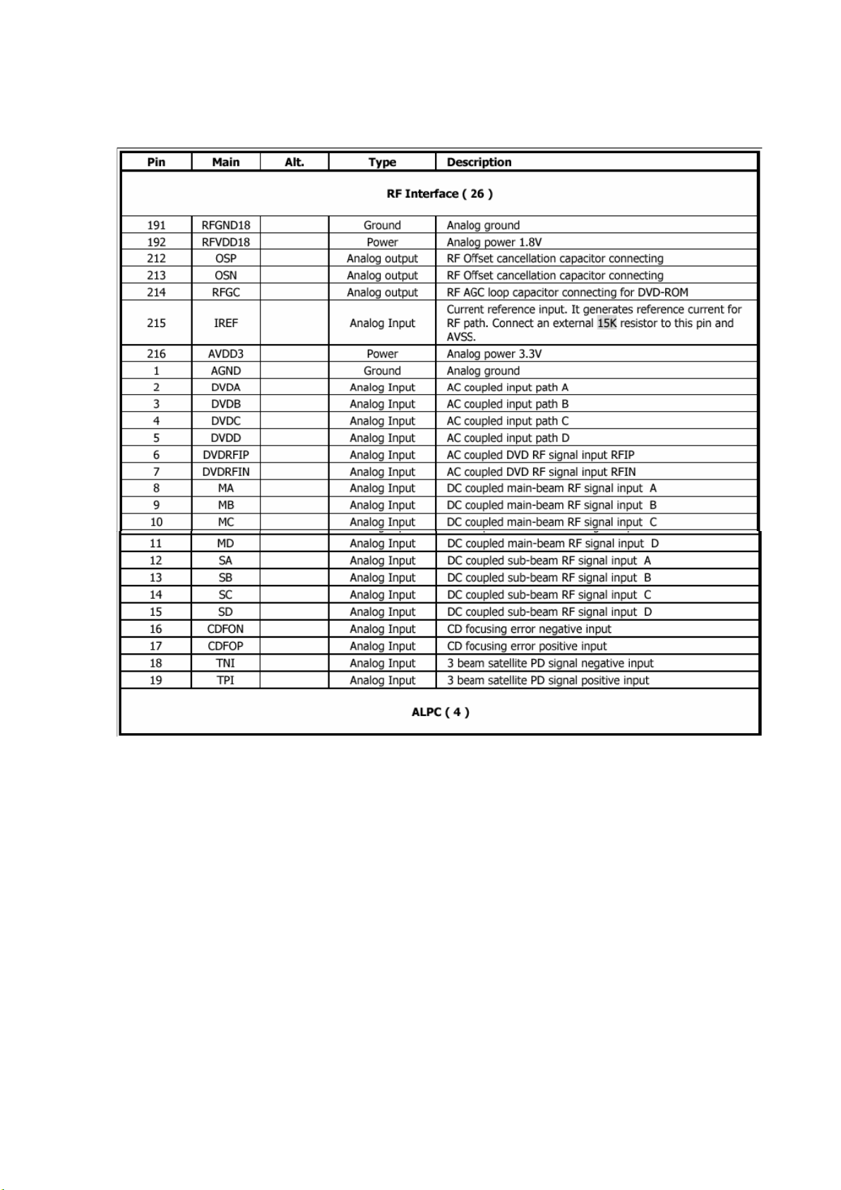
2.2.4.2.1. MT1389D Pin Des cription

2.2.4.2.2. 2 .1 Sytem Block Diagram

A sample system block diagram for the MT1389D DVD player board design is shown in the following figurre:
2.2.4.3. Audio Output
The MT1389D supports two-channel and six-channel analog audio output. In a system configuration with six
analog outputs, the front left and right channels can be configured to provide the stereo (2 channel) outputs and
Dolby Surround, or the left and right front channels for a 5.1 channel surround system. The MT1389D also
provides digital output in S/PDIF format. The board supports both optical and coaxial SPDIF outputs.
2.2.4.4. Audio DACS
The MT1389D supports several variations of an I2S type bus, varying the order of the data bits (leading or no
leading zero bit, left or right alignment within frame, and MSB or LSB first) is possible using the MT1389D
internal configuration registers. The I2S format uses four stereo data lines and three clock lines. The I2S data
and clock lines can be connected directly to one or more audio DAC to generate analog audio output. The twochannel DAC is internal. The six channel DAC is PCM1606. The outputs of the DACs are not differential. The
buffer circuits use National LM833 op-amps to perform the low-pass filtering and the buffering.
2.2.4.5. Video Interface
Video Display Output
The video output section controls the transfer of video frames stored in memory to the internal TV encoder of
the MT1389D. The output section consists of a programmable CRT controller capable of operating either in
Master or Slave mode.
The video output section features internal line buffers which allow the outgoing luminance and chrominance
data to match the internal clock rates with external pixel clock rates, easily facilitating YUV4: 2:2 to YUV4: 2:0
component and sample conversion. A polyphase filter achieves arbitrary horizontal decimation and
interpolation.
Video Bus

The video bus has 8 YUV data pins that transfer luminance and chrominance (YUV) pixels in CCIR601 pixel
format (4:2:2). In this format, there are half as many chrominance (U or V) pixels per line as luminance (Y)
pixels; there are as many chrominance lines as luminance.
Video Post-Processing
The MT1389D video post-processing circuitry provides support for the color conversion, scaling, and filtering
functions through a combination of special hardware and software. Horizontal upsampling and filtering is done
with a programmable, 7-tap polyphase filter bank for accurate non-integer interpolations. Vertical scaling is
achieved by repeating and dropping lines in accordance with the applicable scaling ratio.
Video Timing
The video bus can be clocked either by double pixel clock and clock qualifier or by a single pixel clock. The
double clock typically is used for TV displays, the single for computer displays.
2.2.4.6. Flash Memory
The decoder board supports 70ns Flash memories.
FLASH_512K_8b
The MT1389D permits 8- bit common memory I/O accesses.
2.2.4.7. Serial Eeprom Memory
An I2C serial EEPROM is used to store user configuration (i.e. language preferences, speaker setup, etc.) and
software configuration.. Industry standard EEPROM range in size from 1kbit to 256kbit and share the same IC
footprint and pinout. The default device is 2kbit, 256kx 8, SOIC8 SGS Thomson ST24C02M1 or equivalent.
2.2.4.8. Audio Interface Audio Sampling Rate and PLL Com p o n ent
Configuration
The MT1389D audio mode configuration is selectable, allowing it to interface directly with low-cost audio DACs
and ADCs. The audio port provides a standard I2S interface input and output and S/PDIF (IEC958) audio
output. Stereo mode is in I2S format while six channels Dolby Digital (5.1 channel) audio output can be
channeled through the S/PDIF. The S/PDIF interface consists of a bi-phase mark encoder, which has low skew.
The transmit I2S interface supports the 112, 128, 192, 256, 384, and 512 sampling frequency formats, where
sampling frequency Fs is usually 32 kHz, 44.1 kHz, 48 kHz, 96 kHz, or 192 kHz. The audio samples for the I2S
transmit interface can be 16, 18, 20, 24, and 32-bit samples.
For Linear PCM audio stream format, the MT1389D supports 48 kHz and 96 kHz. Dolby Digital audio only
upports 48 kHz. The MT1389D incorporates a built-in programmable analog PLL in the device architecture in
order to generate a master audio clock. The MCLK pin is for the audio DAC clock and can either be an output
from or an input to the MT1389D. Audio data out (TSD) and audio frame sync (TWS) are clocked out of the
MT1389D based on the audio transmit bit clock (TBCK). Audio receive bit clock (RBCK) is used to clock in
audio data in (RSD) and audio receive frame sync (RWS).
2.2.4.9. Scematics
2.2.4.9.1. Part1

5
4
3
2
1
AL[2]
AR[2]
+12V[1]
R124 470
MUTE_DAC
LCH [4]
RCH [4]
R120
10K
Q28 3906/NC
1 3
2
R171
10K/NC
VCC
DV33
GND
AL
AR
+12V
D17
4.7V
1 2
MUTE
R123
22k
D19 1N4148/NC
1 2
MUTE_DAC
R121
10K
R116
24k
C74 100pF
AL
+
CE31
100uF/16V
13
13
2
Q25
Q15
2
3906
3906
R147 1K
A_MUTE
AR
C75
+
10uF/16v
C79
+
10uF/16v
R117
10k
R125
10k
C77
1000pF
C83
1000pF
R118
5.1k
R122
24k
R126
5.1k
1/2VCC
1/2VCC
-
2
+
3
8 4
+12V
C78 100pF
-
6
+
5
8 4
+12V
1
U13A
NJM4558 OPA
7
U13B
NJM4558 OPA
C76 10uF/16v
+
C80 10uF/16v
+
A_MUTE
A_MUTE
R119
100
R127
100
LCH
Q14
2
2N3904
SOT23
1 3
RCH
Q16
2
2N3904
SOT23
1 3
[1,2,4]
VCC
DV33[1,2,3]
GND[1,2,3,4]
VCC
+12V
MUTE_DAC[2]
LCH
RCH
DV33
R134
10K/NC
D D
C C
B B
+12V
R17210k
CB57
0.1uF
A A
5
R174
R173100k
CE38
+
10k
47uF/16V
1/2VCC
MediaTek Confidential
MediaTek (ShenZhen) Inc.
Title
COMMON1389E_HD60
Document Number
Size
C
AUDIO OUT
Date: Sheet
4
3
2
Rev
changqiao
Drawn:
Checked:
1
Tom Wang
15Saturday, December 09, 2006
3
of

5
+12V
+12V[1]
VCC[1,2,5]
VCC
GND[1,2,3,5]
GND
CVBS
CVBS[2]
R
R[2]
G
G[2]
VB
D D
C C
VB[2]
ASPDIF
ASPDIF[2]
LCH
LCH[5]
RCH
RCH[5]
CVBS
R90
75
G
R78
75
C100
47P
4
+5VV
D25
1 2
1 2
+5VV
D20
1 2
1 2
C104
47P
L28 1.8uH
L27 1.8uH
C105
47P
C101
47P
+5VV
R86
75/NC
0
R88
13
Q10
2
3906/NC
+5VV
R74
75/NC
0
R76
13
Q6
2
3906/NC
1N4148/NC
D27
1N4148/NC
1N4148/NC
D21
1N4148/NC
3
CVBSO
G/Y
2
R178 100
R179 75
C109
C51
0.1uF
ASPDIF
CVBSO
R/V
G/Y
B/U
RGB/CVBS#
ASPECT
LCH
RCH
0.1UF
+
10uF/16v
VCC
R73 33
C52
C112
27PF
C110
100PF
1
2
3
J9
1
2
3
4
5
6
7
8
9
10
TJC3-10AW
C111
100PF
J10
TJC3-3AW
OPTICAL
P=2.54mm
R180
100/NC
1
TP3
L20
10uH/NC
B B
3906
C
+5VV
C48
0.1uF
+5VVVCC
C50
+
47uF/16v/NC
VB
R84
75
L23 1.8uH
C57
47P
EB
R
A A
5
R91
75
L26 1.8uH
C63
47P
4
+5VV
R80
75/NC
0
R82
13
Q8
2
C58
47P
C64
47P
3906/NC
+5VV
R87
75/NC
0
R89
13
Q11
2
3906/NC
+5VV
+5VV
1 2
1 2
1 2
1 2
D24
1N4148/NC
D26
1N4148/NC
D28
1N4148/NC
D29
1N4148/NC
VCC
R181 10K
13
B/U
R/V
3
RGB_SWITCH[ 2 ]
+12V
R183 2K
R184 680
R187 2k
FS0[ 2 ]
FS1[ 2 ]
2
R182 4.7K
Q30
2
9014
1 3
R185
1k
3904 / 3906
Q31
2
2N3904
1 3
Q29
2
3906
RGB/CVBS#
ASPECT
C
BE
R188 2k
MediaTek (ShenZhen) Inc.
Title
Size
Date: Sheet
R186
75
Q32
2
2N3904
1 3
COMMON1389E_HD60
Document Number
Custom
VIDEO OUT
MediaTek Confidential
Drawn:
Checked:
1
changqiao
Tom Wang
25Saturday, December 09, 2006
Rev
3
of
5
DV33[1,2,5]
GND[1,2,4,5]
MA[0..11][2]
BA[0..1][2]
DQM[0..1][2]
DCLK[2]
DCKE[2]
D D
C C
CAS#[2]
RAS#[2]
WE#[2]
CS#[2]
PCE#[2]
PRD#[2]
PWR#[2]
VCC[1]
A[0..20][2]
DCS#
DRAS#
DCAS#
DWE# WE#
R60 33
DBA0 BA0
R61 33
DBA1 BA1
R62 33
SDCKE
R63 33
SDCLK
DRAM
PCE#
PRD#
PWR#
VCC
A[0..20]
FLASH
RN1
7 8
5 6
3 4
1 2
33x4
DV33
GND
MA[0..11]
BA[0..1]
DQM[0..1]
DCLK
DCKE
CAS#
RAS#
WE#
CS#
CS#
RAS#
CAS#
DCKE
DCLK
C107
10PF
MA0
MA1
MA2
MA3
MA4
MA5
MA6
MA7
MA8
MA9
MA10
MA11
DBA0
DBA1
SDCLK
SDCKE
DCS#
DRAS#
DCAS#
DWE#
DQM0
DQM1
U8
23
A0
24
A1
25
A2
26
A3
29
A4
30
A5
31
A6
32
A7
33
A8
34
A9
22
A10/AP
35
A11
20
BA0/A13
21
BA1/A12
38
CLK
37
CKE
19
CS
18
RAS
17
CAS
16
WE
15
DQML
39
DQMH
36
NC
40
NC
54
VSS
41
VSS
28
VSS
ESMT M12L64164A/N.C
TSOP54
DQ0
DQ1
DQ2
DQ3
DQ4
DQ5
DQ6
DQ7
DQ8
DQ9
DQ10
DQ11
DQ12
DQ13
DQ14
DQ15
VCC
VCC
VCC
VCCQ
VCCQ
VCCQ
VCCQ
VSSQ
VSSQ
VSSQ
VSSQ
4
DQ7
2
DQ6
4
DQ5
5
DQ4
7
DQ3
8
DQ2
10
DQ1
11
DQ0
13
DQ8
42
DQ9
44
DQ10
45
DQ11
47
DQ12
48
DQ13
50
DQ14
51
DQ15
53
SD33
1
14
27
SD33
3
9
43
49
6
12
46
52
MA0
MA1
MA2
MA3
MA4
MA5
MA6
MA7
MA8
MA9
MA10
DBA0
SDCLK
SDCKE
DBA1
DRAS#
DCAS#
DWE#
DQM0
DQM1
U7
21
A0
22
A1
23
A2
24
A3
27
A4
28
A5
29
A6
30
A7
31
A8
32
A9
20
A10
19
BA/A11
35
CLK
34
CKE
18
CS
17
RAS
16
CAS
15
WE
36
DQMHNCVCCQ
33
NC
37
26
VSS
50
VSS
ESMT M12L16161A-7
3
DQ0
DQ1
DQ2
DQ3
DQ4
DQ5
DQ6
DQ7
DQ8
DQ9
DQ10
DQ11
DQ12
DQ13
DQ14
DQ15
VCC
VCC
VCCQ
VCCQDQML
VCCQ
VSSQ
VSSQ
VSSQ
VSSQ
2
DQ0
2
DQ1
3
DQ2
5
DQ3
6
DQ4
8
DQ5
9
DQ6
11
DQ7
12
DQ8
39
DQ9
40
DQ10
42
DQ11
43
DQ12
45
DQ13
46
DQ14
48
DQ15
49
SD33
1
25
SD33
7
1314
38
44
4
10
41
47
DV33 SD33
L29 FB
CB43
0.1uF
CE25
+
47uF/16v
SD33
CB44
0.1uF
CB38
0.1uF
CB45
0.1uF
CB39
0.1uF
CB46
0.1uF
CB40
0.1uF
CB47
0.1uF
CB41
0.1uF
DQ[0..15][2]
CB42
0.1uF
1
DQ[0..15]
DRAM
FLASH
IIC
AD[0..7]
SCL
SDA
AD[0..7][2]
SCL[2,3]
SDA[2,3]
A20 AA20
16Mb
R64 0/NC
A1
R70
10k
PCE#
PRD#
PWR#
A2
A3
A4
A5
A6
A7
A8
A9
A10
A11
A12
A13
A14
A15
A16
A17
A18
A19
AA20
B B
CB52
0.1uF
FVCC
R68
10k
FVCC
DV33 FVCC
R85 0
CE26
10uF/16v
A A
5
CB50
+
0.1uF
U9
25
A0
24
A1
23
A2
22
A3
21
A4
20
A5
19
A6
18
A7
8
A8
7
A9
6
A10
5
A11
4
A12
3
A13
2
A14
1
A15
48
A16
17
A17
16
A18
9
A19
10
A20
26
CE
28
OE
11
WE
12
RESET
IC FLASH MX29LV800 8Mb
4
D10
D11
D12
D13
D14
D15/A-1
WP/ACC
BYTE
VCC
GND1
GND2
D0
D1
D2
D3
D4
D5
D6
D7
D8
D9
AD0
29
AD1
31
AD2
33
AD3
35
AD4
38
AD5
40
AD6
42
AD7
44
30
32
34
36
39
41
43
A0
45
14
47
37
27
46
FVCC
CB53
0.1uF
U11
1
NC
2
3
4 5
VCC
NC
WP
NC
SCL
GND SDA
EEPROM 24C02
SOP8
8
7
6
GND
SCL
SDA
DV33
DV33
R67
R65
1k
1k
MediaTek Confidential
MediaTek (ShenZhen) Inc.
Title
COMMON1389E_HD60
Rev
3
of
1
Drawn:
Checked:
changqiao
Tom Wang
35Saturday, December 09, 2006
Document Number
Size
B
SDRAM&FLASH
Date: Sheet
3
2
5
RFV33
C16
2200pF
R32 10k
R33 10k
R35 100k
FB
L13
CE34
+
100uF/16v
Q4
2
1 3
R40 10
R41 10
Q5
13
2
VOTK+
VOTKVOLD+
VOLDPGND
VNFTK
PVCC2
PREGND
VINLD
CTK2
CTK1
VINTK
BIAS
STBY
RFV33
V1P4
AVCC1
CB14
0.1uF
IOA
2
47uF/16v
AVCC1
CE15
DV33
V2P8
+
L10
1.8uH
CE16
47uF/16v
C
B
A
D
RFO
C
B
A
D
1
B
ADACVDD3
+
RFVDD3
C
E
V1P4
CB15
0.1uF
C29 1uF
C31 1uF
C32 1uF
3
C37
NC
V18
CB18
0.1uF
C21
6800pF
C0603/SMD
V20
C30 1uF
R38
V18
ADIN
OP-
OP+
R17
680k
VCC
C
1
3
C
E
B
2SB1132
8550
8550
14
VOFC+
13
VOFC-
12
VOSL+
11
VOSL-
10
PGND
9
PVCC1
8
VCC
2930
G1G2
7
VNFFC
6
VOSL
5
VINSL-
4
VINSL+
3
CF2
2
CF1
1
VINFC
LDO2
CE21
+
47uF/16v
RFV33
+
CE22
LDO1
47uF/16v
FF+
R44
1
SPSP+SL-
V1P4
R55 20k
FOSO
CE24
+
47uF/16v
C4 2200pF
R11 680k
R15
150k
R20 NC
R23 1
SP-
D D
SP+
LIMIT
SLSL+
DV33
R24 10k
0603
DV33
V18
D
2
1
2SK3018
1
2
3
4
5
6
7
8
9
10
11
12
13
14
15
TOP
16
17
18
19
20
21
22
23
24
25 26
R42
1
MO_VCC
C43
150pF
L11 10uH
47uF/16v
L37 FB
CE36
+
47uF/16v
R31 100k
S
3
2
Q2
2SK3018
GND
LD-DVD
AVCC1
MDI1
LD-CD
E
AVCC1
V20
GND
F
B
A
RFO
IOA
D
C
R43
1
SL+
CB34
0.1uF
DV33
C C
G
B B
HA1
HEADER 24 SMD0.5 TOP
A A
R51 20k
CE19
R58
10k
CB17
0.1uF
FMSO
TRSO
V1P4
STBY
C5
0.1uF/NC
OPO
R12 0
R16
150k
J2
6
5
4
3
2
1
PH2.0-6AW
AADVDD3DV33
+
C28
6800pF
C0603/SMD
RFV33
C108
100NF
RFV18
2N3904
2
Q1
1 3
13
2N3904
13
2
Q3
2SK3018
C38
0.1uF
CB19
0.1uF
U4
T-
15
16
17
18
19
T+
20
21
22
23
24
25
26
27
28
CD5954
CB36
0.1uF
5
CE17
+
47uF/16v
R19
6.8
ADACVDD3
C33 1uF
E
F
MDI1
LDO2
LDO1
C36
0.1uF
NC
R45
1
R52
10k
MO_VCC
CB16
0.1uF
4
+
4
C6
0.1uF
CE14
10uF/16v
CC
BB
AA
DD
V2P8
V20
V1P4
TEZISLV
OPO
OPOP+
DMO
FMO
TROPEN
TRO
FOO
ADIN
STBY
A2
A3
A4
A5
A6
A7
A8
A18
A19
DV33
FOSO
TRSO
FMSO
DMSO
C44
150pF
RFVDD3
V1P4
+
R53
20k
CE18
47uF/16v
C39
330pF
PLLVDD3
CB13
0.1uF
C40
330pF
DMSO
1
2
3
4
5
6
7
8
9
10
11
12
13
14
15
16
17
18
19
20
21
22
23
25
26
27
28
29
30
31
32
33
34
35
36
37
38
39
40
41
42
43
44
45
46
47
48
49
50
51
52
53
54
V1P4
R13 100k
R18 15k
C20 0.1uF
RFVDD3
C22 0.1uF
C26
0.1uF
AGND
DVDA
DVDB
DVDC
DVDD
DVDRFIP
DVDRFIN
MA
MB
MC
MD
SA
SB
SC
SD
CDFON
CDFOP
TNI
TPI
MDI1
MDI2
LDO2
LDO1
SVDD3
CSO/RFOP
RFLVL/RFON
SGND
V2REFO
V20
VREFO
FEO
TEO
TEZISLV
OP_OUT
OP_INN
OP_INP
DMO
FMO
TROPENPWM
PWMOUT1/ADIN0
TRO
FOO
FG/ADIN1
GPIO0/VSYNC#
GPIO1/HSYNC#
GPIO2
IOA2
DVDD18
IOA3
IOA4
IOA5
IOA6
IOA7
HIGHA0
C41
0.1uF
VCC MO_VCC
213
216
21524214
IREF
RFGC
AVDD3
IOA18
IOWR#
IOA19
57
A16
PWR#
DV33
R46 20k
R47 18k
R48 15k
R49 10k
C42
0.015uF
L31 FB
C23 0.033uF
C27
210
212
211
OSP
OSN
RFGND
CRTPLP
HIGHA6
DVDD3
HIGHA7
A16
A14
A15
A13
R50 10k
R54 10k
V1P4
209
HRFZC
HIGHA5
20pF
1000pF
C17
0.1uF
208
207
RFRPAC
HIGHA4
63
A11
A12
3
C10
RFVDD3
RFRPDC
206
C9 0.1uF
RFVDD3
RFVDD3
204
205
ADCVSS
C24 0.047uF
C25 0.047uF
203
202
LPFIN
LPFOP
ADCVDD3
C11
10uF/16v
+
C15 0.47uF/N.C
XIXTALI
PLLVDD3
JITFO
JITFN
198
197
196
201
200
199
194
195
JITFN
JITFO
LPFIP
XTALI
LPFON
PLLVSS
PLLVDD3
IDACEXLP
MT1389E
Pin Assignment v1.4
HIGHA2
HIGHA3
65646261605958
A10
66
A9
FOO
TRO
FMO
DMO
HIGHA1
IOA20
A20
PCE#
IOCS#
IOA1
6880695667
A1
70
PRD#
AD5
AD4
DVSS
AD2
AD1
AD0
IOOE#
AD3
77
7655747372
71
75
AD2
AD5
AD3
AD4
AD0
AD1
LOADLOAD+
TROUT
TRIN
VCC
3
XO
RFV18
192
193
XTALO
RFVDD18
AD6
IOA21
78
79
AD6
TRCLOSE
191
RFGND18
ALE
PH2.0-5AW
C3 390pF
JITFO
R9 750k
C12
+
10uF/16v
ADACVDD3
ADACVDD3
AL
189
185
186
188
190
187
AVCM
ALF(CTR)
AL/SDATA2
ADACVDD1
ADACVDD2
ALS/SDATA0
AD7
IOA0
A17
DVDD18
UWR#
URD#
81
83
82
8485868788899091929394
A17
AD7
A0
V18
J4
5
4
3
2
1
VCC
R8 2K
R4 100
C13
1500pF
AR
184
182
181
183
ARS
ARF(SW)
AR/SDATA1
DVDD3
UP1_2
UP1_3
IOA
VSCK
R83 1
180
179
178
APLLVSS
ADACVSS2
ADACVSS1
GPIO6
UP1_4
UP1_5
SCL
VSTB
VSDA
Q24
2
JITFN
APLLVDD3
AADVDD3
177
176
AADVDD
APLLCAP
APLLVDD
UP1_6
UP1_7
UP3_0
95
SDA
3
1
+
10uF/16v
ADVCM
175
174
AKIN1
UP3_1
96
97
RXD
TP4
MOVCC
8550
Q9
8050
C14
173
AKIN2
ADVCM
UP3_4
UP3_5
9899100
TXD
VB
R
171
170
172
AADVSS
R/Cr/CVBS/SY
GPIO7
ICE
101
TRCLOSE
URST#
Q21
8550
DACVDD3
CB12
0.1uF
G
169
168
B/Cb/SC
DACVSSA
G/Y/SY/CVBS
PRST#IRINT0#
102
103
IR
3
1
CB11
0.1uF
CVBS
DACVDD3
DACVDD3
164
167
166
165
163
CVBS
DACVSSB
DACVSSC
DACVDDA
DACVDDB
DACVDDC
MC_DATA
ASDATA3
ASDATA2
ASDATA1
ASDATA0
RD6
DQM0#
RD7
RD5
DVDD3
106
104
105
107
108
DQ7
DQM0
DQ6
DQ5
use DIP decal
R5 100
2
Q20
8050
FS
VREF
SPDIF
ALRCK
ACLK
ABCK
GPIO5
DVSS
GPIO4
GPIO3
DVDD18
RA4
RA5
RA6
RA7
RA8
RA9
RA11
CKE
DVDD3
RCLK
RA3
RA2
RA1
DVDD18
RA0
RA10
BA1
BA0
RCS#
RAS#
CAS#
RWE#
DQM1
RD8
RD9
DVSS
RD10
RD11
RD12
RD13
RD14
RD15
RD0
RD1
RD2
RD3
RD4
U3
MT1389E
LQFP216/SMD
R7 2K
CE13
+
47uF/16v
162
161
160
159
158
157
156
155
154
153
152
151
150
149
148
147
146
145
144
143
142
141
140
139
138
137
136
135
134
133
132
131
130
129
128
127
126
125
124
123
122
121
120
119
118
117
116
115
114
113
112
111
110
109
C45
0.1UF
TROPEN
LOAD-
2
L30 10UH
DV33
LOAD+
2
DV33
DV33
R14 100k
R175
33
XI XO
V18
DACVDD3
ASPDIF
MUTE_DAC
RGB_SWITCH
MA4
MA5
MA6
MA7
MA8
MA9
MA11
DCKE
DCLK
MA3
MA2
MA1
MA0
MA10
BA1
BA0
CS#
RAS#
CAS#
WE#
DQM1
DQ8
DQ9
DQ10
DQ11
DQ12
DQ13
DQ14
DQ15
DQ0
DQ1
DQ2
DQ3
DQ4
VREF
FS0
FS1
Y1
C18
27MHz
33pF
FS
C34
0.1uF
TROUT
TRIN
LIMITV18
TxD
RxD
DV33
RS-232
CB20
CB21
0.1uF
0.1uF
CB26
CB25
0.1uF
0.1uF
CB31
0.1uF
1
R10
URST#
VCC
DV33
GND
VSCK
VSDA
VSTB
PCE#
PWR#
MUTE_DAC
RGB_SWITCH
A[0..20]
AD[0..7]
PRD#
PWR#
PCE#
MA[0..11]
DQ[0..15]
BA[0..1]
DQM[0..1]
DCLK
DCKE
CAS#
RAS#
WE#
CS#
SCL
SDA
ASPDIF
1
10
+
CE12
10uF/16v
DC4
IR
AL
AR
FS0
FS1
CVBS
R
G
VB
VIDEO INTERFACE
FLASH
BA[0..1] [3]
DQM[0..1] [3]
DCLK [3]
DCKE [3]
CAS# [3]
RAS# [3]
WE# [3]
CS# [3]
MEMORY
AUDIO INTERFACE
Drawn:
Checked:
A[0..20] [3]
AD[0..7] [3]
PRD# [3]
PWR# [3]
PCE# [3]
MA[0..11] [3]
DQ[0..15] [3]
IIC
ASPDIF [4]
APLLVDD3
CB10
0.1uF
R176
33
C19
33pF
R26
560
J3
4
3
2
1
PH2.0-4AW
V18
CB32
0.1uF
CB28
0.1uF
CB23
0.1uF
DV33
DV33
CB24
0.1uF
CB30
0.1uF
CB33
0.1uF
CB27
0.1uF
CB22
0.1uF
MediaTek Confidential
MediaTek (ShenZhen) Inc.
Title
COMMON1389E_HD60
Document Number
Size
C
MT1389E LQFP 216
Date: Sheet
DV33
URST# [1]
[1,4,5]
VCC
DV33 [1,3,5]
GND [1,3,4,5]
IR [1]
VSCK [1]
VSDA [1]
VSTB [1]
PCE# [3]
PWR# [3]
AL [5]
AR [5]
MUTE_DAC [5]
RGB_SWITCH [4]
FS0 [4]
FS1 [4]
CVBS [4]
R [4]
G [4]
VB [4]
SCL [3]
SDA [3]
changqiao
Tom Wang
45Saturday, December 09, 2006
of
Rev
3
5
4
3
2
1
COMMON1389E_HD60_V3
MT1389E (LQFP216) D V D MP Board for SANYO HD60 PUH
1 INDEX & POWER, RESET
2 MT1389E
3 SDRAM & FLASH
D D
4 VIDEO OUT & AV-CON
5 AUDIO OUT - WM8766
+5VCC
+3.3VCC
+12VCC
DV33
R2
10K
DEVICE
SUPPLY
MT1389E
MT1389E
MT1389E
OP AMP.
Audio DAC
Audio DAC
R3
R177
R1
10k
10k
Rev
V1
Initial released. Modified from 3-SY1389DP1-V11
History
P#
Date
2005.01.19
V2 Add SCART and VGA output 2005.03.01
Modify Video backend circuit.
V3
+12VCC
L35 FB
CE5
100uF/25v
+5VCC
VCC
10
+
CE1
10uF/16v
L36 FB
100uF/16v
+3.3VCC
L32
FB
CE10
+12V
CB5
+
0.1uF
VCC
+
CB8
0.1uF
AZ-1117 3.3V/NC
3
IN
+
U10
CE2
100uF/16v
+3.3VCC
2
OUT
GND
1
DV33
CB3
0.1uF
+
CE39
100uF/16v/NC
2005.03.09
DV33
D3
1N4148
RESET Circuit
R6
10k
URST#
CE9
+
10uF/16v
DC4
+12V
URST#
IR
DV33
VCC
GND
+12V [4 5 ]
URST# [ 2 ]
IR [ 2 ]
DV33 [ 2,3,5]
VCC
GND [ 2,3,4,5]
VSCK[2]
VSDA[2]
VSTB[2]
[ 2,4,5 ]
VSCK
VSDA
VSTB
NAME
VCC
DV33
RFV33
AV33 Laser Diode 3.3V
V18
SD33
+12V
-12V Audio -12V OP AMP.
AVDD5
DVDD3
C C
B B
TYPE
Digital 5V
Digital 3.3V
Servo 3.3V
Digital 1.8V
Digital 3.3V SDRAM
Audio +12V
Audio 5V
Audio 3.3V
CON1
6
5
4
3
2
1
TJC3-6AW
HEAD6-2.54/H
P=2.54mm
CON2
TJC3-6AW
P=2.54mm
6
5
4
3
2
1
IRVCC
VSDA
VSCK
VSTB
C1
10pF
IR
+
CE7
100uF/16v
V18
CB7
0.1uF
MediaTek Confidential
MediaTek (ShenZhen) Inc.
Title
COMMON1389E_HD60
Document Number
Size
C
INDEX
Date: Sheet
2
Rev
changqiao
Drawn:
Checked:
1
Tom Wang
55Saturday, December 09, 2006
3
of
L33
FB
+
CE37
100uF/16v
A A
FM1
FM2
5
4
3
D11
1N4007
D9
1N4007
2.3. AK57 Service Menu
S-No OSD Tanım
( Definition )
001 FAPS First APS ON = Aktif
002 ISPM I2C Modu
( I2C Mode )
003 INIT Yazılım ve donanım resetleme
( Resetting software and hardware )
Mümkün Ayarlar
( Possible Settings )
OFF = İn-Aktif
ON = Active
OFF = In-active
OFF OFF
ON = Resetleme aktif
OFF = Resetleme in-aktif
ON = Enable resetting
OFF = Disable resetting
Table 1 Init
S-No OSD Tanım
( Definition )
004 AGCSPD IF AGC hızı
( IF AGC speed )
005 AGCTO AGC Take over 0..63 31
Mümkün Ayarlar
( Possible Settings )
0 = Yavaş
1 = Standart
2 = Hızlı
3 = Hız seviyesi 2’ den daha
yüksek
0 = Slow
1 = Standard
2 = Fast
3 = Fastest
Varsayılan Değer
( Default )
OFF
OFF
Varsayılan Değer
( Default )
1
Table 2 AGC Servis ayarları ( AGC Service settings )
S-No OSD Tanım
( Definition )
006 COFF Cut – Off Ayarı
( Cut-Off setting )
Table 3 VG2 Alignment Servis ayarları ( VG2 Alignment Service settings )
Mümkün Ayarlar
( Possible Settings )
0..63 32
Varsayılan Değer
( Default )

S-No OSD Tanım
( Definition )
007 VERT SLOP Dikey eğim (VSL), SBL biti yarı blank’e
anahtarlanmalıdır.
( Vertical slope (VSL), SBL bit should be
keyed to half-blank.)
008 SCORRECTION S-doğrulaması (SC)
( S-correction (SC) )
009 VERT SHIFT 4:3 Wide Screen için dikey kaydırma
( 4:3 vertical shifting for Wide Screen )
010 VERT AMP Dikey genlik (VA)
( Vertical Amplitude (VA) )
011 HOR SHIFT Yatay kaydırma
( Horizontal shifting )
012 VERT SHIFT16 16:9 Wide Screen için dikey kaydırma
( 16:9 vertical shifting for Wide Screen )
013 VERT AMP16 16:9 Dikey genlik
( 16:9 Horizontal amplitude )
014 RGB HSH 50 Hz’lik RGB modunda yatay kaydırma
( In RGB mode with 50 Hz, horizontal
shifting )
015 RGB HSH60 60 Hz’lik RGB modunda yatay kaydırma
( In RGB mode with 60 Hz, horizontal
shifting )
016 60HZ HSH 43 4:3 MODE 60 Hz yatay kaydırma
( In 4:3 MODE with 60 Hz, horizontal
shifting )
017 60HZ VSH 43 4:3 MODE 60 Hz dikey kaydırma
( In 4:3 MODE with 60 Hz, vertical
shifting )
018 60HZ VA 43 4:3 MODE 60 Hz dikey genlik
( In 4:3 MODE with 60 Hz, vertical
amplitude )
019 60HZ VSH 169 16:9 MODE 60 Hz dikey kaydırma
( In 16:9 MODE with 60 Hz, vertical
shifting )
020 60HZ VA 169 16:9 MODE 60 Hz Dikey genlik
( In 16:9 MODE with 60 Hz, vertical
amplitude )
Mümkün Ayarlar
( Possible Settings )
0..63 32
0..63 32
0..63 32
0..63 32
0..63 32
0..63 32
0..63 32
0..63 37
0..63 37
0..63 31
0..63 31
0..63 31
0..63 31
0..63 31
Varsayılan Değer
( Default )
Table 4 Geometri Servis ayarları ( Geometry Service settings )

S-No OSD Tanım
( Definition )
021 QSS Qss amfi mode değiştirici
( Switching the mode of the QSS amplifier )
022 OIF IF-PLL’de DC ofset doğrultması
( DC offset correction at IF-PLL )
023 IF PLL demodulatör frekansı
( PLL demodulator frequency )
024 OFR Frekans Girişi Aktivasyonu: Installation
menüsündeki Tuning Mode olan Frekans modunu
aktif veya pasif hale getirir.
( Frequency Entry Activation: Frequency mode
which is value Tuning Mode item on the
Installation menu can be enabled or disabled by
OFR. )
025 FFI IF-PLL Hız filtresi
( Fast filter IF-PLL )
026 BS1 (Gerekli ayarlamayı yapmak için ilgili Tuner
dökümanına bakılmalıdır.)
( Please look at the related Tuner specification for
necessary adjustments. )
027 BS2 (Gerekli ayarlamayı yapmak için ilgili Tuner
dökümanına bakılmalıdır.)
( Please look at the related Tuner specification for
necessary adjustments. )
028 BS3 (Gerekli ayarlamayı yapmak için ilgili Tuner
dökümanına bakılmalıdır.)
( Please look at the related Tuner specification for
necessary adjustments. )
029 CB (Gerekli ayarlamayı yapmak için ilgili Tuner
dökümanına bakılmalıdır.)
( Please look at the related Tuner specification for
necessary adjustments. )
Mümkün Ayarlar
( Possible Settings )
ON = QSS Aktif
OFF = QSS İn-aktif
ON = QSS Active
OFF = QSS In-Active
0..63 29
0 = 58.75 MHz
1 = 45.75 MHz
2 = 38.90 MHz
3 = 38.00 MHz
4 = 33.40 MHz
5 = 42.00 MHz
6 = 33.90 MHz
7 = 48.00 MHz
8 = EXTERNAL
ON = Aktif
OFF = İn-aktif
ON = Active
OFF = In-Active
ON =Hızlı zaman
sabiti
OFF = Normal zaman
sabiti
ON = Fast time
constant
OFF = Normal time
constant
0..15 1
0..15 2
0..15 4
0..255 142
Varsayılan Değer
( Default )
ON
2
ON
OFF

S-No OSD Tanım
( Definition )
030 B1-H (Gerekli ayarlamayı yapmak için ilgili Tuner
dökümanına bakılmalıdır.)
( Please look at the related Tuner specification for
necessary adjustments. )
031 B1-L (Gerekli ayarlamayı yapmak için ilgili Tuner
dökümanına bakılmalıdır.)
( Please look at the related Tuner specification for
necessary adjustments. )
032 B2-H (Gerekli ayarlamayı yapmak için ilgili Tuner
dökümanına bakılmalıdır.)
( Please look at the related Tuner specification for
necessary adjustments. )
033 B2-L (Gerekli ayarlamayı yapmak için ilgili Tuner
dökümanına bakılmalıdır.)
( Please look at the related Tuner specification for
necessary adjustments. )
Table 5 Tuning Servis ayarları ( Tuning Service settings )
S-No OSD Tanım
( Definition )
034 FRAV AV için Peaking merkezi frekansı
( For AV, Peaking center frequency )
035 YSCM SECAM için Y-delay ayarı
( For SECAM, Y-delay setting )
036 YNTS NTSC için Y-delay ayarı
( For NTSC, Y-delay setting )
037 YPAL PAL için Y-delay ayarı
( For PAL, Y-delay setting )
038 YAV1 AV-1 için Y-delay ayarı
( For AV-1, Y-delay setting )
039 YSVHS SVHS için Y-delay ayarı
( For S-VHS-2, Y-delay setting )
Mümkün Ayarlar
( Possible Settings )
0..255 12
0..255 32
0..255 30
0..255 2
Mümkün Ayarlar
( Possible Settings )
0 = 2.7 Mhz
1 = 3.1 Mhz
2 = 3.5 Mhz
0..15 12
0..15 2
0..15 2
0..15 4
0..15 4
Varsayılan Değer
( Default )
Varsayılan Değer
( Default )
1
Table 6 Video Servis ayarları ( Video Service settings )
S-No OSD Tanım
( Definition )
040 WPRC Cold için White point Red
Mümkün Ayarlar
( Possible Settings )
0..63 32
Varsayılan Değer
( Default )

S-No OSD Tanım
( Definition )
( For Cold, White point Red )
041 WPGC Cold için White point Green
( For Cold, White point Green )
042 WPBC Cold için White point Blue
( For Cold, White point Blue )
043 BLORB Black seviyesi ofset Red – Blue
( Black level offset Red – Blue)
044 BLOG Black seviyesi ofset Green
( Black level offset Green )
045 WPRN Normal için White point Red
( For Normal, White point Red )
046 WPGN Normal için White point Green
( For Normal, White point Green )
047 WPBN Normal için White point Blue
( For Normal, White point Blue )
048 BLRB-RGB RGB için Black seviyesi ofset Red – Blue
( For RGB, Black level offset Red – Blue )
049 BLG-RGB RGB için Black seviyesi ofset Green
( For RGB, Black level offset Green )
050 WPRW Warm için White point Red
( For Warm, White point Red )
051 WPGW Warm için White point Green
( For Warm, White point Green )
052 WPBW Warm için White point Blue
( For Warm, White point Blue )
053 BLRB-YUV YUV için Black seviyesi ofset Red – Blue
( For YUV, Black level offset Red – Blue )
054 BLG-YUV YUV için Black seviyesi ofset Green
( For YUV, Black level offset Green )
055 WPRW-RGB RGB için White point Red
( For RGB, White point Red )
056 WPGW-RGB RGB için White point Green
( For RGB, White point Green )
057 WPBW-RGB RGB için White point Blue
( For RGB, White point Blue )
Mümkün Ayarlar
( Possible Settings )
0..63 32
0..63 31
0..63 32
0..63 32
0..63 37
0..63 32
0..63 19
0..63 32
0..63 32
0..63 49
0..63 40
0..63 25
0..63 32
0..63 32
0..63 32
0..63 40
0..63 32
Varsayılan Değer
( Default )
Table 7 White ton ayarları ( White tone adjustments )

S-No OSD Tanım
( Definition )
058 OSO Dikey overscan’de Switch-off
( Switch-off at vertical overscan )
059 FSL Dikey sync için Forced Slicing seviyesi
( For vertical sync, Forced Slicing level )
060 PN8-STB If option is ON TV can open from stanby
when PIN8 is activated
061 PWL Peak white sınırlayıcı
( Peak white limiting )
062 BPS Bypass chroma temel-band
( Bypass chroma base-band )
063 CLPL Soft kırpma seviyesi
( Soft clipping level )
064 CL Katot drive seviyesi
( Cathode drive level )
065 ST-LMI Option for sleep timer last minute
indicator
Mümkün Ayarlar
( Possible Settings )
ON = Aktif Switch-off
OFF = İn-aktif Switch-off
ON = Enable Switch-off
OFF = Disable Switch-off
ON = Sync genliği %60’ı
sabit seviyede bulunan
dikey slicing
OFF = Otomatik dikey
slicing seviyesi
Vertical slicing level
ON =
Varsayılan Değer
( Default )
ON
OFF
fixed to 60% of sync
amplitude
OFF =
Automatic vertical
slicing level
OFF = feature is not
avaliable
ON = feature is avaliable
0..15 8
ON = Bypass temel-band
kroma gecikme çizgisi
OFF = Temel-band
kroma gecikme çizgisi
aktif
Bypass baseband
ON =
OFF
OFF
chroma delay line
OFF = Baseband chroma
delay line active
0 = PWL‘in 0% üstünde
1 = PWL’in 5% üstünde
2 = PWL’in 10% üstünde
3 = İn-aktif
0 = 0% above PWL
1 = 5% above PWL
2 = 10% above PWL
3 = Off
0..15 10
last minute
ON =
0
OFF
indicator appears on TV
OFF = last minute
indicator does not appear
on TV

S-No OSD Tanım
( Definition )
066 DNMENU Dynamic Menu Mode ON = Dynamic Menu
Mümkün Ayarlar
( Possible Settings )
Enable
OFF = Dynamic Menu
Disable
Varsayılan Değer
( Default )
OFF
067 UK-EU IDTV UK veya PAN-EU OFF = 0 UK
(IDTV UK)
ON = 1 PAN-EU
(IDTV PAN-EU)
Table 8 Bit Kontrol Servis ayarları ( 8 Bit Control Service settings )
S-No OSD Tanım
( Definition )
068 FAVI FAV
( FAV )
069 BAVI BAV
( BAV )
070 BSVI SVHS
( SVHS )
071 SSTDBG BG ses standardı
( BG sound standard )
072 SSTDI I ses standardı
( I sound standard )
073 SSTDDK DK ses standardı
( DK sound standard )
074 SSTDL L- L prime ses standardı
( L- L prime sound standard )
Mümkün Ayarlar
( Possible Settings )
ON = Aktif
OFF = İn-aktif
ON = Active
OFF = In-active
ON = Aktif
OFF = İn-aktif
ON = Active
OFF = In-active
ON = Aktif
OFF = İn-aktif
ON = Active
OFF = In-active
ON = Aktif
OFF = İn-aktif
ON = Active
OFF = In-active
ON = Aktif
OFF = İn-aktif
ON = Active
OFF = In-active
ON = Aktif
OFF = İn-aktif
ON = Active
OFF = In-active
ON = Aktif
OFF = İn-aktif
ON = Active
OFF
Varsayılan Değer
( Default )
ON
OFF
OFF
ON
ON
ON
ON
S-No OSD Tanım
( Definition )
Mümkün Ayarlar
( Possible Settings )
OFF = In-active
Varsayılan Değer
( Default )
Table 9 Kaynak seçimi Servis seçenekleri ( Source Switching Service settings)
S-No OSD Tanım
( Definition )
075 TXHPOS Teletext tek sayfa başlangıç noktası ayarları
( One page Teletext starting point setting )
076 TXTBRI Teletext parlaklık ayarı
( Teletext brightness setting )
077 TXTCON Teletext contrast ayarı
( Teletext contrast setting )
078 LSEL1 Menü dili seçimi
( Menu language setting )
079 LSEL2 Menü dili seçimi
( Menu language setting )
080 -------
Mümkün Ayarlar
( Possible Settings )
0..20 10
0..63 32
0..15 0
0..255 255
0..255 255
Varsayılan Değer
( Default )
Table 10 Teletext Servis seçenekleri ( Teletext Service settings )
S-No OSD Tanım
( Definition )
081 PWPRF Açılışta görüntü ve sesin gelmesine göre, fast
startup ve perfect startup.
( According to video and sound, when TV
opening, fast startup and perfect startup )
082 PWRES STANDBY’dan açılır.
( Opens from STANDBY. )
Table 11 Güç Servis seçenekleri ( Power Service settings )
S-No OSD Tanım
( Definition )
Mümkün Ayarlar
( Possible Settings )
0..15
0 = Fast
15 = Perfect
ON = Son duruma
gore açılır
OFF = STANDBY’dan
açılır
ON = Opens
depending on the
last state
OFF = Opens from
STANDBY
Mümkün Ayarlar
( Possible Settings )
Varsayılan Değer
( Default )
10
ON
Varsayılan Değer
( Default )

083 MAXCOL Picture menüsündeki maksimum renk ayar
sınırlayıcısı
(Maximum color setting limiter at Picture menu )
084 MAXBRI Picture menüsündeki maksimum parlaklık ayar
sınırlayıcısı
(Maximum brightness setting limiter at Picture
menu )
085 MINBRI Picture menüsndeki minimum parlaklık ayar
sınırlaması
(Minimum brightness setting limiter at Picture
menu)
086 MAXCON Picture menüsündeki maksimum contrast ayar
sınırlayıcısı
(Maximum contrast setting limiter at Picture
menu )
0..63 50
0..63 57
0..63 20
0..63 50
Table 12 Picture Servis seçenekleri ( Picture Service settings )
S-No OSD Tanım
( Definition )
087 SAVEFS Fabrika Servis ayarlarını saklama
( Saving Factory settings )
088 LOADFS Fabrika Servis ayarlarını yükleme
( Loading Factory setting )
089 OAVL Ses menusunde AVL’i optional yapar
(AVL is optional in sound menu)
OAVL = 0 (AVL is off and AVL line is not
avaliable in sound menu)
OAVL = 1 (AVL line is avaliable in sound menu)
OAVL = 2 (AVL is on and AVL line is not
avaliable in sound menu)
Other values of OAVL work like OAVL =1
090 HTLSRC Selection for hotel mode search
HTLSRC = 0 (TV)
HTLSRC = 1 (AV)
HTLSRC = 2 (FAV)
HTLSRC = 3 (SVHS)
HTLSRC > 3 (HOTEL MODE NOT AVAILABLE)
091 HMAXVOL Maximum volume for hotel mode 0-63 32
092 HDEFVOL Volume level definition for hotel mode when tv
is openning
093 RPO Preover Shoot Ratio
PSYS_RATIO_PRE_OVERSHOOT_MIN =0
PSYS_RATIO_PRE_OVERSHOOT_MAX =3
Mümkün Ayarlar
( Possible Settings )
OFF OFF
OFF OFF
0-63 32
0-63 32
0-63 32
0-3 32
Varsayılan Değer
( Default )

094 PF Peaking Frequency
PF1-PF0 = 0 (2.7 Mhz)
1 (3.1 Mhz)
2 (3.5 Mhz)
3 (spare)
095 APSSND Default value of sound standard in APS menu
0-> BG
1-> I
2-> DK
3-> L\L’
096 SRCO Control DVD,IDTV, AV2 (Only AK58) sources
0-> DVD, AV2 are OFF
1-> DVD is ON. AV2 is OFF
2-> AV2 is ON. DVD is OFF
3-> DVD, AV2 are ON
0-3 2
0-3 0
0-7 0
Table 13 Fabrika Servis ayarları ( Factory Service settings )
Geometri ayarları : Service menüsündeki 007-011 satırlar arasındaki 50Hz geometri ayarları yapıldıktan sonra, NTSC
offsetlerin belirlenmesi için 016-018 satırlar arasındaki NTSC 60Hz ayarları yapılır. NTSC ayarlarını her tüp çalıması için
bir kez yapılması yeterlidir. Çünkü NTSC ayarları yapılırken, NTSC offset değerleri hesaplanarak EEPROM da saklanır.
16:9 Zoom modu ayarlarıda NTSC ayarları gibi yapılır ve 16:9 offset değerleri hesaplanarak EEPROM’da saklanır. Daha
sonra 50 Hz geometri ayarları değiştirildiğinde, 007-011 veya 016-018 satırlar arasında iken menü tusuna basılarak
geometri ayarları kaydedildiğinde, otomatik olarak 16:9 modu, RGB horizontal shift ve NTSC geometri değerleri
hesaplanır. RGB horizontal shift offset değerleri koda gömülü haldedir. NTSC ve 16:9 modu offset değeri EEPROM’da
saklanmaktadır.
Geometry Adjustment: After adjusting 50Hz geometry items (between 007-011). NTSC 60 Hz geometry items
(between 016-018) should be adjusted to determine NTSC 60Hz offset. NTSC offset is automatically calculated and
stored in NVM. Later on, if we need to change 50Hz geometry settings, NTSC 60Hz geometry settings is automatically
calculated by using NTSC offset. 16:9 mode geometry adjustment works like NTSC 60Hz geometry adjustment.
If press to menu button between 007-011 or 016-018 items. New geometry setting is stored and, 16:9 mode, RGB
shift and NTSC geometry automatically calculated. RGB shift offset value is stored in software. Only NTSC offset and
16:9 mode offset values are stored in EEPROM.
AGC ayarı : Tunere 60db yayın verildikten sonra AGCTO iteminin uzerine gelinip mavi tuşa basıldıgında AGC otomatik
olarak ayarlanır.
AGC adjustment: Connect to tuner 60db broadcast and, press to blue button on AGCTO item. AGC is automatically
adjusted.
Screen Ayarı: Servis menüsünde sarı tuşa basılarak, dikey tarama iptal edilir ve screen ayarının yapılabilmesi için ilgili
registerlar güncellenir. Ekranda ince bir çizgi belirir. Daha sonar bu ince çizgi en ince hale gelene kadar screen
potansiyometrisi ayarlanır. Tekrar sarı tuşa basıldığında eski ayarlar geri yüklenir.
Screen Adjustment: When yellow button is pressed in service menu. Vertical scan is disabled and related registers
are updated. Thin line will be appeared on the screen. Then the screen potentiometer is gently adjusted until the
thin line will be lightly disappeared When press to yellow button again, old register values are reloaded and vertical
scan is enabled.
FOCUS Ayarı : TV de yayın verilir. . FOCUS potansiyometresi en uygun değerede ayarlanır.
FOCUS Adjustment: TV is tuned to the signal. Then focus potantiometer (the upper pot on the rear side of the FBT
transformer) is adjusted for optimum focusing drive.
2.4. TUNER SETTINGS
VHF1-VHF3 VHF3-UHF AK56 SERVICE MENU ITEMS
Frq. (Mhz) Frq. (Mhz) B1-H B1-L B2-H B2-L BS1 BS2 BS3 CB
Philips UV1316S MK3 156,25 MHz 441,25 MHz 012 050 030 02 001 002 004 142
LG TAEW-G002D 140,25 Mhz 431.25 Mhz 011 050 029 098 001 002 008 142
Thomson CTT5020 114,25 MHz 401,25 MHz 009 146 027 130 003 006 133 142
Samsung TECC2949PG28B
Samsung TECC2949PG35B 170,25 MHz 449,25 MHz 013 018 030 130 001 002 008 142
Alps TEDE9X226A 142,25 MHz 425,25 MHz 011 082 029 002 001 002 008 142
Alps TEDE9-004A 149,25 MHz 424,25 MHz 011 194 028 242 001 002 008 142
Samsung TECC2949PG40B 142,25 MHz 425,25 MHz 011 082 029 002 001 002 008 142
Samsung TECC2949PS40B 142,25 MHz 425,25 MHz 011 082 029 002 001 002 008 142
According to Reference Divider 62.5 Khz apply the following formula
Value = ( Frequency (Mhz) * 1000 ) / ( 62.5 ) + 622 ;
Binary_value ( 2 bytes ) = ToBinary( value );
x can be 1 or 2
Bx-H = MSByte( Binary_value ); ( most significant byte )
Bx-L = LSByte( Binary_value ); ( least significant byte )
170,25 MHz 465,25 MHz 013 018 031 130 001 002 004 142
Explanations
B1H High byte of VHF1-VHF3 cross-over frequency
B1L Low byte of VHF1-VHF3 cross-over frequency
B2H High byte of VHF3-UHF cross-over frequency
B2L Low byte of VHF3-UHF cross-over frequency
BS1 Band switching byte for VHF1
BS2 Band switching byte for VHF3
BS3 Band switching byte for UHF
CB Control byte
 Loading...