

VESTEL 11AK49 Service Manual
Date
: 20/
06/2005
SERVICE MANUAL
UOC III AK49
Version : V1.0
Unit : Electronic Hardware Design

VESTEL R&D Service Manual
1
?
AK49-001
TABLE OF CONTENTS
1. INTRODUCTION 4
1.1. Purpose 4
1.2. Scope 4
1.3. General Features 4
2. GENERAL DESCRIPTION 5
2.1. Introduction 5
2.2. System Building Blocks 5
2.2.1. UOC-III (Ultimate-One-Chip) 5
2.2.1.1. Fav & B_Svhs & F_Svhs 8
2.2.1.2. Scart1 8
2.2.1.3. Scart2 8
2.2.1.4. Scart3 9
2.2.1.5. VestelBus 9
2.2.1.6. Audio 9
2.2.1.7. Port Allocations 10
2.2.1.8. Power Management 11
2.2.1.9. Input & Output Performance 12
2.2.1.10. Feature Board 14
Copyright 2003 VESTEL Group of Company
All rights reserved. Passing on and copying of this document, use and communication of its contents not permitted without written permission from VESTEL
2.2.2. Audio Block 15
2.2.2.1. Audio Power Amplifier 15
2.2.2.2. Headphone Amplifier 17
2.2.2.3 Pop Noise Protection Circuit 18
2.2.3. Deflection & Display Block 19
2.2.3.1. Horizontal Deflection 19
2.2.3.2. Vertical Deflection 20
2.2.3.3. CRT Board 22
2.2.3.4. Rotation 23
2.2.3.5. X-RAY Protection 24
2.2.3.6. Dynamic Focus 24
2.2.3.7 Screen & Focus Short Circuit Protection 25
2.2.4. SMPS BLOCK 28
2.2.4.1. Primary Block 28

VESTEL R&D Service Manual
2
?
AK49-001
2.2.4.2. Secondary Block 29
2.2.5 CABELING 31
2.2.6 CABLE SPECs 33
2.2.6.1 RGB CABLE 33
2.2.6.2 200V CABLE (with BSVM) 35
2.2.6.3 200V CABLE (with BSVM) 37
2.2.7 SAW FILTER 39
2.2.8 TUNER 40
3. AK49 CHASSIS MANUAL ADJUSTMENTS PROCEDURE 41
3.1 SMPS B+ADJUSTMENT 41
3.2 AFC ADJUSTMENT 41
3.3 FOCUS ADJUSTMENT 41
3.4 SCREEN ADJUSTMENT 42
4. AK49 CHASSIS PRODUCTION SERVICE MODE ADJUSTMENTS 43
5. MENU LANGUAGE TABLE 74
6.PICTURE MODES 75
7. CIRCUIT DIAGRAMS 79
8. APPENDIX 84
Copyright 2003 VESTEL Group of Company
All rights reserved. Passing on and copying of this document, use and communication of its contents not permitted without written permission from VESTEL

VESTEL R&D Service Manual
3
?
AK49-001
Document History
Document
Versi
Date
on
Revision and
Status Prepared by Approved by
Review
History
v1.0 20.06.2005 MUHAMMED M.
KAYA
SERDAR GÜLTEN
File Name: AK49_SM_V1.0
KAGAN M. PANCAR
Copyright 2003 VESTEL Group of Company
All rights reserved. Passing on and copying of this document, use and communication of its contents not permitted without written permission from VESTEL

VESTEL R&D Service Manual
4
?
AK49-001
1. Introduction
1.1. Purpose
This document is prepared for the UOC3 TV project and describes the whole system features and
operating principles to be used in hardware design phase.
The document is based on “Device Specification UOCIII-Version 2.5” and “Introducing UOC-III” from
Philips Semiconductors.
1.2. Scope
The document covers detailed descriptions of AK49 chassis system building blocks.
1.3. General Features
AK49 is a 110? / 50 Hz. chassis which is capable of driving CRT sizes in the range of 24” – 33”,
including realflat and 16:9 CRT’s . The chassis has the following main features;
? Remote Control
? Colour Standards ; PAL, SECAM, NTSC,
? Transmission standards ; B/G, L/L’ I/I’, DK,
? Teletex ; 10 pages,
? Intercarier/QSS sound proccessing,
? Multi-standard alignment free PLL tuning,
? PIP, PAP, POP, PAT, TAT ,
Copyright 2003 VESTEL Group of Company
All rights reserved. Passing on and copying of this document, use and communication of its contents not permitted without written permission from VESTEL
? CTI option ,
? 2D Comb Filter ,2D/4H
? Headphone with volume control,
? SubWoofer option,
? 2 Full Scart with SVHS availability via Scart-2 , Scart-3 / BAV, FAV and F_SVHS /B_SVHS,
? BSVM option,
? Dynamic Focus option,
? Rotation (Tilt) option,
? NICAM/GERMAN Stereo,
? Virtual Dolby option,
? 2 x 10W (%10 THD),
? YPbPr input feature,
? TV-DVD Combi ,
? IDTV ,
? TV-R/HDD,
? EPG,

VESTEL R&D Service Manual
5
?
AK49-001
2. General Description
2.1. Introduction
This chapter describes system building blocks and their detailed discriptions.
2.2. System Building Blocks
AK49 chassis main block are;
? UOC3 : Microcontroller + Video Proccessor + Sound Proccessor + IF+Teletext
? SMPS : SMPS Controller, SMT, Bridge Rect., Line Filters
? HV Block : FBT, HOT, Vertical Amplifier, Line Driver, EW Amp.
? AUDIO : Audio Amp., DAC, Comperator.
? CRT BOARD : RGB Amp.
? Feature Board : PIP, CTI IC’s.
2.2.2 UOC-III (ULTIMATE-ONE-CHIP)
UOC3 is composed of microcontroller, video proccessor, sound proccessor and IF blocks. So, there
are digital and anolog parts in it named as Picasso and Cosmic respectively as shown below ;
Copyright 2003 VESTEL Group of Company
All rights reserved. Passing on and copying of this document, use and communication of its contents not permitted without written permission from VESTEL
UOC3 has standard and face down versions, pin squence differs between two version. After
investigation of the pining it is decided to use face down version for layout compability.

VESTEL R&D Service Manual
6
?
AK49-001
Copyright 2003 VESTEL Group of Company
All rights reserved. Passing on and copying of this document, use and communication of its contents not permitted without written permission from VESTEL
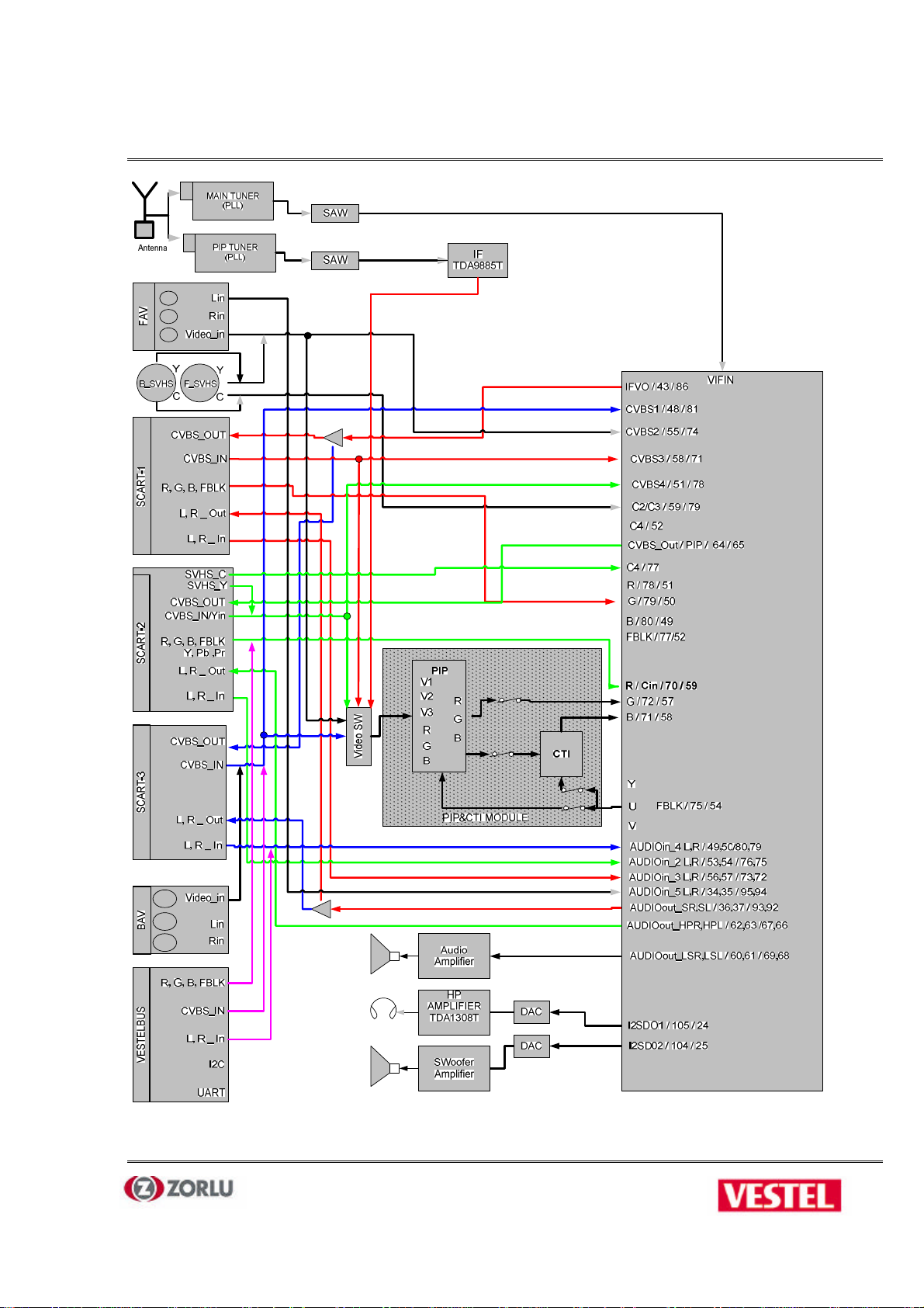
Block diagram of the TV System with face-down version is;
VESTEL R&D Service Manual
7
?
AK49-001
Copyright 2003 VESTEL Group of Company
All rights reserved. Passing on and copying of this document, use and communication of its contents not permitted without written permission from VESTEL

VESTEL R&D Service Manual
8
?
AK49-001
2.2.2.1 FAV & BAV & B_SVHS & F_SVHS
B_SVHS and F_SVHS inputs can not be supported at the same time.
FAV & B_SVHS_Y & F_SVHS_Y inputs use same CVBS input. (cvbs2/74)
B_SVHS_ C & F_SVHS_C input is C2/C3(70).
FAV audio input is AUDIOin_5 L,R (94,95) and shared with F_SVHS.
BAV video input is CVBS1 (81) and can not be supported with SCART3 at the same time.
BAV audio input is AUDIOin_4 L,R (80,79) and shared with SCART3.
2.2.2.2 SCART1
SCART1 video input is (CVBS3/71) . SCART1 video input is also applied to Video Switch
IC(TEA6415C) for PIP application.
SCART1 video out will use (IFVO/86) front_end video output, that output is also used as SCART3
video output via a buffer circuit.
SCART1 RGB/fblk inputs are R(51), G(50), B(49), FBLK(52) .
SCART1 AUDIO input is AUDIOin_3 L,R ( 73,72) .
SCART1 AUDIO output is AUDIOout_SR,SL (93,92). Same output also used as SCART3 Audio output.
2.2.2.3 SCART2
Copyright 2003 VESTEL Group of Company
All rights reserved. Passing on and copying of this document, use and communication of its contents not permitted without written permission from VESTEL
SCART2 video input is CVBS4 (78) . SCART2 video input is also applied to Video Switch IC(TEA6415C)
for PIP application.
SCART2 supports SVHS input. SVHS / C input is C4 (77) , Y input is use same video input.
SCART2 video output is CVBSO/PIP (65). That video output is selectable, all inputs can be selected to
be output from SCART2.
SCART2 RGB inputs are R(59), G(57), B(58), FBLK/INSSW2 (54), except CTI/PIP option.
At PIP application ;
- There are PIP_CVBS, SCART1, SACRT2, SCART3, FAV video inputs and RGB, FBLK inputs to PIP IC.
- If there is no CTI application, PIP output is applied to SCART2 RGB input directly.
- In case of PIP&CTI combined application, PIP output will be input to CTI IC as YUV. The YUV
output of CTI IC will be applied to R/Vin(59), G/Yin(57), B/Uin(58) as YUV.

VESTEL R&D Service Manual
9
?
AK49-001
YPbPr input is possible via SCART2 RGB lines with an adaptor.
In this case R/Vin(59), G/Yin(57), B/Uin(58) inputs can be used as;
- RGB,
- YUV,
- YPbPr inputs.
SCART2 audio inputs are AUDIOin_2 L,R ( 75) .
SCART2 audio outputs are AUDIOout_HPR,HPL (67,66). That output is also selectable .
2.2.2.4 SCART3
SCART3 video input is CVBS1 (81) . That input will also be used as optional BAV video input. and
applied to Video Switch IC(TEA6415C) for PIP application.
SCART3 video output will be SCART1 video output via a buffer circuit.
SCART3 audio inputs are AUDIOin_4 L,R (80,79). These audio inputs will also used for optional BAV
L,R and VESTELBUS L,R audio inputs.
SCART3 audio out will be through SCART1 audio outputs via a buffer circuit.
2.2.2.5 VESTELBUS(IDTV,DVD-Combi)
VESTELBUS video input is CVBS1 (81), so VESTELBUS will not be supported with SCART3 at the same
time.
Copyright 2003 VESTEL Group of Company
VESTELBUS RGB inputs are SCART2 RGB inputs, so in case of VESTELBUS option SCART2 RGB
is not supported.
VESTELBUS UART input ;
- TXD TX (1),
- RXD RX (2),
- IRQ_DVB INT2 (3).
VESTELBUS I2C input is standard I2C bus.
2.2.2.6 AUDIO
Main audio out is AUDIOout_LSR,LSL (69,68).
All rights reserved. Passing on and copying of this document, use and communication of its contents not permitted without written permission from VESTEL
Selectable HP out is I2SD01 24) out to DAC.
Subwoofer out is I2SD02 (25) out to DAC.

VESTEL R&D Service Manual
10
?
AK49-001
2.2.2.7 PORT ALLOCATIONS
(32) (INT-0) REMOTE
(31) (INT-1) TV_LINK
(30) (Counter-Timer) PROTECTION
(27) (I2S Word Select) I2S_WS
(26) (I2S Clock) I2S_CLK
(25) (I2S OUT2) I2S_Swoofer
(24) (I2S OUT1) I2S_HP
(23) (I2S-IN/OUT) WRITE-PROT.
(22) (ON/OFF) ON/OFF+LED
(21) (SCL) SCL
(20) (SDA) SDA
(18) (PWM) ROT/TILT
(17) (PWM0) PAP_LOW
(16) (PWM1) SW
(15) (PWM2) S_RESET
Copyright 2003 VESTEL Group of Company
All rights reserved. Passing on and copying of this document, use and communication of its contents not permitted without written permission from VESTEL
(14) (ADC0) AV1_STAT
(13) (ADC1) AV2_STAT
(10) (ADC2) AV3_STAT/DVD SENSE
(9) (ADC3) KEYB.+SERV.
(7) (PWM3) MUTE
(6) (PWM4) SAW_SW
(3) (INT2) IRQ/DVB
(2) (UARTBUS) RXD
(1) (UART BUS) TXD
VESTEL R&D Service Manual
11
?
AK49-001
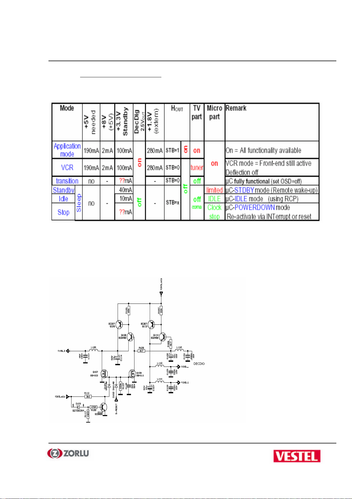
2.2.2.8 POWER MANAGEMENT
The power consumption of UOC3 is ;
Only 3,3V_Stb is necessary for the start-up. IC internally produces 2,5V and 1,8V at the Standby
mode. After start-up necessary 1,8V are produced by external regulators. So, we have 3,3V_Stb, 5V,
5V_Stb and 1,8V. for UOC3. We don’t have 8V. even for audio outputs (1,2V RMS achieved with 5V).
All the voltages are produced by SMPS except 1,8V.
RESET :
Copyright 2003 VESTEL Group of Company
All rights reserved. Passing on and copying of this document, use and communication of its contents not permitted without written permission from VESTEL
1V8 digital and 1V8 analogue are produced by using 2V5 DECDIG-signal. DECDIG-signal is given

VESTEL R&D Service Manual
12
?
AK49-001
to base of Q108 Transistor and base of Q114 Transistor. The collector voltage becomes 1v8.
When the +3V3_stb voltage decreases below the 2V6 Q110 Transistor goes OFF condition so FETs
become ON. Q107 FET shorts 1V8 digital to ground and system is reset condition.
Another reset condition becomes when the S_Reset port is active. While S_Reset port is active, FETs
become ON. 1V8 digital is shorted to ground.
All the supply architecture of the UOC3 is as follows;
Copyright 2003 VESTEL Group of Company
All rights reserved. Passing on and copying of this document, use and communication of its contents not permitted without written permission from VESTEL
VESTEL R&D Service Manual
13
?
AK49-001
2.2.2.9 INPUT & OUTPUT PERFORMANCE
EXTERNAL INPUT - OUTPUT PERFORMANCE
CVBS INPUT VOLTAGE
CVBS OUTPUT VOLTAGE
VIDEO OUTPUT IMPEDANCE
RGB INPUT VOLTAGE
AUDIO INPUT VOLTAGE
AUDIO OUTPUT VOLTAGE
AUDIO INPUT IMPEDANCE
AUDIO OUTPUT IMPEDANCE
PIN 8 SWITCHING Standard
PRIORITY BETWEEN SCARTS Vestel Standard
RECEPTION PERFORMANCE
USABLE MINIMUM SIGNAL LEVEL
USABLE MAXIMUM SIGNAL LEVEL
COLOUR KILLER LEVEL
SOUND KILLER LEVEL
SYNCHRONISING SENSITIVITY LEVEL
FM GERMAN STEREO SENSITIVITY LEVEL
NICAM STEREO SENSITIVITY LEVEL
Copyright 2003 VESTEL Group of Company
BTSC STEREO SENSITIVITY LEVEL NO BTSC
NOISE LIMITED SENSITIVITY LEVEL
TELETEXT EYEHEIGHT LEVEL
CLOSED CAPTION SENSITIVITY LEVEL NO CLOSED CAPTION
AFC PULL IN RANGE
TUNER RECEIVING RANGE
All rights reserved. Passing on and copying of this document, use and communication of its contents not permitted without written permission from VESTEL
1 ? 0.15 V
Luminance 700 ± 15 % mV
Sync 300 ± 15 % mV
p_p
pp
pp
Burst 300 ± 15 % mVpp
DC level 2 V dc
75 ± 10 % O
1 ? 15 % V
500 ? 15 % Mv
500 ? 15 % mV
p_p
rms
rms
minimum 10 K?
maximum 1 KO
50 dBµV
90 dBµV
32 dBµV
30 dBµV
35 dBµV
40 dBµV
40 dBµV
30 dB?V
% 45
-500 KHz / +800 KHz
± 5 MHz

VESTEL R&D Service Manual
14
?
AK49-001
2.2.2.10 FEATURE BOARD ( PIP & CTI )
PIP&PAP and CTI applications performed with that feature board. For PIP&PAP application Micronas
SDA9488/SDA9489 and for CTI application Toshiba TA1366FG is used.
There is a socket on the board for external YUV input which will be used for DVD or IDTV application
with PIP&PAP and CTI feature. There are switches on the board for adaptation of application
configurations.
Only CTI Application
YUV output from UOC3 comes to CTI IC TA1366FG and goes back to UOC3 .
CTI & IDTV or DVD
CTI & PIP Application
YUV output from UOC3 comes to CTI IC TA1366FG , then inputs to PIP IC SDA9488. Any desired
external CVBS signal is directed to PIP IC via video switch and used for PIP picture on CTI applied
video signal. That video signal goes back to UOC3 as YUV.
Copyright 2003 VESTEL Group of Company
All rights reserved. Passing on and copying of this document, use and communication of its contents not permitted without written permission from VESTEL

VESTEL R&D Service Manual
15
?
AK49-001
2.2.3 AUDIO BLOCK
2.2.3.1 AUDIO AMPLIFIER
TDA8928J 2X10W class D amplifier is used for audio amplification. It is supplied by +14V and –14V to
give 2X10W output to 8ohm. loads by %10 THD.
Copyright 2003 VESTEL Group of Company
All rights reserved. Passing on and copying of this document, use and communication of its contents not permitted without written permission from VESTEL

VESTEL R&D Service Manual
16
?
AK49-001
Audio inputs Main_L and Main_R is applied via voltage comparator LM393 to amplifier. PWM
swicthing outputs are then filtered by 33UH and 470NF.
SOUND PERFORMANCE
SOUND CALL UP TIME Max. 4 sec.
MAXIMUM AUDIO OTPUT POWER (RF INPUT) 10W
MAXIMUM AUDIO OTPUT POWER (EXTERNAL INPUT) 10W
THD AT MAXIMUM AUDIO OUTPUT POWER (RF INPUT) %10
THD AT MAXIMUM AUDIO OUTPUT POWER (EXTERNAL INPUT) %10
THD AT 50 mW AUDIO OUTPUT POWER (RF INPUT) %3 (IC spec.)
THD AT 50 mW AUDIO OUTPUT POWER (EXTERNAL INPUT) %3 (IC spec.)
SIGNAL TO NOISE RATIO (RF INPUT) 50 db.
SIGNAL TO NOISE RATIO (EXTERNAL INPUT) 40 dB
SIGNAL TO BUZZ RATIO 40 dB
CROSSTALK: TV TO AV - AV TO TV 60 dB
RESIDUAL SOUND (RF INPUT) 20 mW/rms
RESIDUAL SOUND (EXTERNAL INPUT) 20 mW/rms
FREQUENCY RESPONSE (RF INPUT) 100 Hz – 10 kHz
FREQUENCY RESPONSE (EXTERNAL INPUT) 100 Hz – 10 kHz
BASS FREQUENCY RESPONSE (RF INPUT) 10 ± 2 dB
BASS FREQUENCY RESPONSE (EXTERNAL INPUT) 10 ± 2 dB
TREBLE FREQUENCY RESPONSE (RF INPUT) 10 ± 2 dB
TREBLE FREQUENCY RESPONSE (EXTERNAL INPUT) 10 ± 2 dB
POP NOISE 5 Vpp
HORIZONTAL HUM NOISE 15 mVrms
VERTICAL HUM NOISE 15 mVrms
VIDEO NOISE ON THE AUDIO OUTPUT 50 mVpp
Copyright 2003 VESTEL Group of Company
All rights reserved. Passing on and copying of this document, use and communication of its contents not permitted without written permission from VESTEL

VESTEL R&D Service Manual
17
?
AK49-001
2.2.3.2 HEADPHONE AMPLIFIER
Headphone output is achieved by I2S out. I2S output is converted to anolog signal by DAC
CS4334 and then applied to TDA1308T amplifier.
Copyright 2003 VESTEL Group of Company
SubWoofer output is achieved by the same way, I2S ouptut is converted to analog signal by DAC
CS4334 and applied to external SubWoofer amplifier board.DAC CS4334 will work at a rate of 32Fs
MCLK/LRCK = 512, 256 or 128 and De-emphasis feature of CS4334 is disabled.
HEADPHONE PERFORMANCE
MAXIMUM AUDIO OUTPUT POWER (RF INPUT) 22,5 ± 2,5 mWrms
MAXIMUM AUDIO OUTPUT POWER (EXTERNAL INPUT) 22,5 ± 2,5 mWrms
THD AT MAXIMUM AUDIO OUTPUT POWER (RF INPUT) %10
THD AT MAXIMUM AUDIO OUTPUT POWER (EXTERNAL INPUT) %10
THD AT 0.5 mW AUDIO OUTPUT POWER (RF INPUT) %1
THD AT 0.5 mW AUDIO OUTPUT POWER (EXTERNAL INPUT) %1
All rights reserved. Passing on and copying of this document, use and communication of its contents not permitted without written permission from VESTEL
SIGNAL TO NOISE RATIO (RF INPUT) 40 dB
SIGNAL TO NOISE RATIO (EXTERNAL INPUT) 40 dB

VESTEL R&D Service Manual
18
?
AK49-001
2.2.2.3 POP NOISE PROTECTION CIRCUIT
This circuit is used to prevent pop noise in AC turn-off. While TV is working due to +14V. T1
is OFF . In turn-0ff situation BE voltage of T1 becomes negative and transistor goes to ON
condition ,so it drives T2 and T2 pull-down mute pin to perform muting.
Copyright 2003 VESTEL Group of Company
All rights reserved. Passing on and copying of this document, use and communication of its contents not permitted without written permission from VESTEL

VESTEL R&D Service Manual
19
?
AK49-001
2.2.3 DEFLECTION & DISPLAY BLOCK
2.2.3.1 Horizontal Deflection
Deflection block consist of following main parts,
Horizontal driver transistor (Q601),
Horizontal driver (TR600),
HOT (Horizontal Output Transistor) (Q600),
FBT (TR601),
E/W transistor (Q602),
E/W coil (L601),
E/W injection Coil (Bridge Coil) (L602),
Linearity Coil (L603),
Flyback Capacitors (C608, C607),
S-correction capacitor (C615 ve C613),
Modulated S-correction capacitor (C611),
Hdrive signal is buffered and applied to line driver transistor by a capacitor.
Line driver produces necessary base currents, parallel diode to base series resistor speeds up the
reverse base current.
UOC3 has soft-start and soft-stop features to have more safe operation. There are two base current
adjustment resistors on the circuit. Collector current differs according to CRT sizes .
Tube dependent components are choosen to fit best picture performance by keeping;
11,5 usec. Flyback time,
Copyright 2003 VESTEL Group of Company
All rights reserved. Passing on and copying of this document, use and communication of its contents not permitted without written permission from VESTEL
Max. 1300V. collector voltage (peak-detect mode measurement)
Max. 500V. at the diode modulator cathode (D605).
Max. 20V. (peak-detect mode measurement) at the E/W transistor drain.
Max. 200V video B+ voltage.

VESTEL R&D Service Manual
20
?
AK49-001
2.2.3.2 Vertical Deflection
TDA8359J (IC502) vertical amplifier is used for vertical deflection. It’s 3,2A. current capability makes
it enable to drive all 50Hz. CRT screen sizes.
Differential vertical drive signals; resistor network at inputs are chosen CF type to
minimize temperature sensitivity of TV set. Those resistors can be changed to MF type in
case of heat run failure.
Power resistor R633, R634 values will change according to CRT sizes.
Copyright 2003 VESTEL Group of Company
All rights reserved. Passing on and copying of this document, use and communication of its contents not permitted without written permission from VESTEL

VESTEL R&D Service Manual
21
?
AK49-001
Copyright 2003 VESTEL Group of Company
All rights reserved. Passing on and copying of this document, use and communication of its contents not permitted without written permission from VESTEL
VESTEL R&D Service Manual
22
?
AK49-001
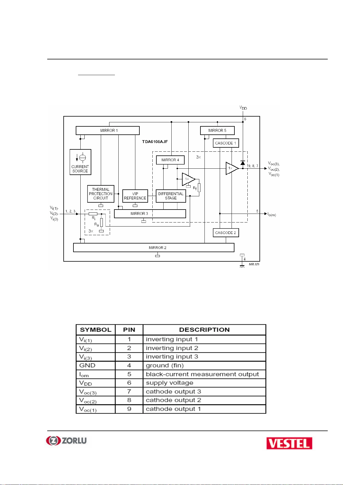
2.2.3.3 CRT Board
TDA6108AJF is used as RGB amplifier. Main feature of that triple amplifier is the increased fixed gain
of 81. It’s 8 MHz. Bandwidth at 100Vpp video signal makes it enable to use in all 50Hz. TV
applications.
Copyright 2003 VESTEL Group of Company
All rights reserved. Passing on and copying of this document, use and communication of its contents not permitted without written permission from VESTEL
VESTEL R&D Service Manual
23
?
AK49-001
CRT board have single and double focus CRT socket options.
There are CC type 1,5K series flash current limiting resistors (R903, R904, R905) on the RGB lines. In
addition to resistors BAV21 clamp diodes (IC901,IC902,IC903) are introduced.
Spot Killer circuit pulls G1 to –200V by Q700 at turn off instant.
BSVM amplifier circuit modulates the beam to have sharper images at the adges of CRT. Basicly, it
amplifies the software delayed controlled BSVM signal and apply it to BSVM winding of neck.
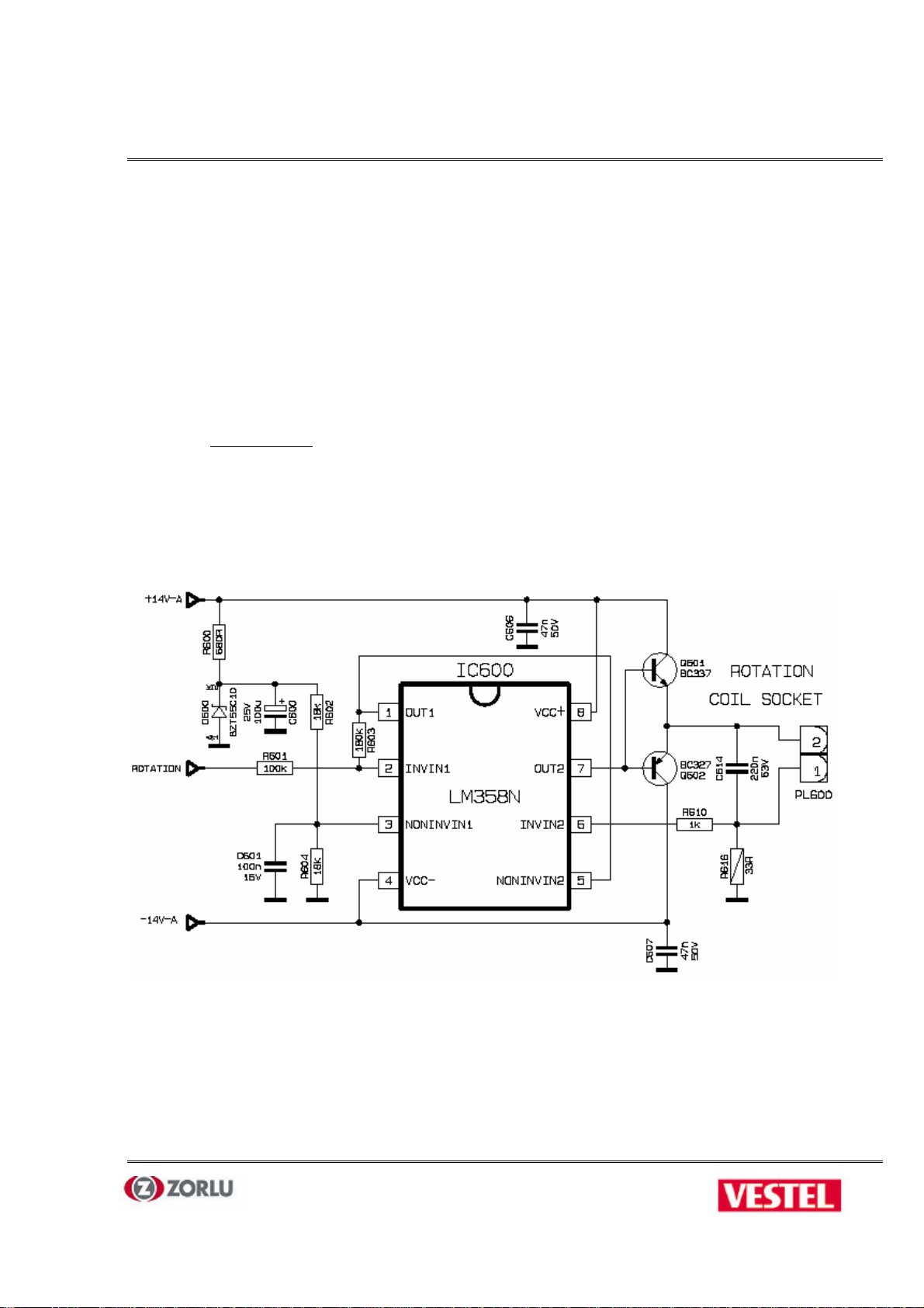
2.2.3.4 ROTATION
PWM rotation output of UOC3 is first converted to DC then applied to rotation circuit. OPAMP LM358N
(IC600) and medium power transistors (Q601, Q602) performs DC amplification necessary for rotation
coil.
Copyright 2003 VESTEL Group of Company
All rights reserved. Passing on and copying of this document, use and communication of its contents not permitted without written permission from VESTEL

VESTEL R&D Service Manual
24
?
AK49-001
2.2.3.5 X-RAY PROTECTION
This circuit is used to protect the system X-ray caused by HV. While Anode voltage is bellow 33kv, T1
is off due to 80 volt because BE voltage of T1 becomes negative. While Anode voltage is above 33 kv.
80 voltage increases, it becomes approximately 90 volt. At that condition T1 is ON due to 90 volt
because BE voltage of T1 becomes positive, so it drives protection.
2.2.3.6 DYNAMIC FOCUS
Copyright 2003 VESTEL Group of Company
All rights reserved. Passing on and copying of this document, use and communication of its contents not permitted without written permission from VESTEL
E/W injection signal is converted to sinus shape after it passes LC circuit. Then the signal is amplified
via coil and applied to Dynamic focus.
VESTEL R&D Service Manual
25
?
AK49-001
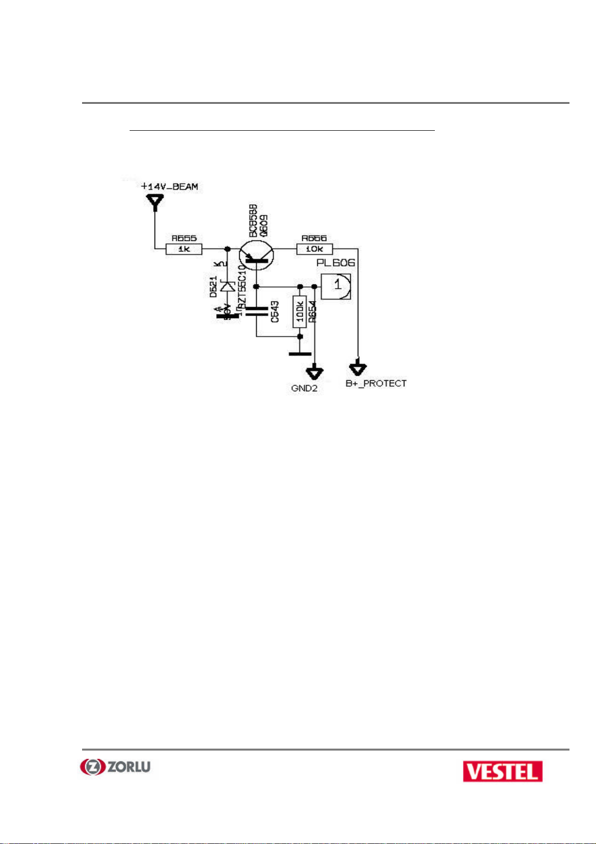
2.2.3.7 SCREEN & FOCUS SHORT CIRCUIT PROTECTION
Above circuit is used for protection against screen & focus grounding. Basicly the base
of PNP transistor Q609 is connected to screen&focus potentiometer of FBT, in another words
FBT focus pack is connected to ground via R654. The voltage at the base of that transistor is
Copyright 2003 VESTEL Group of Company
normally higher then the zener voltage at the emitter. When any short circuit occurs at focus
or screen the base voltage is decreased to a value lower then zener voltage, that forces
transistor to conduction and trigers another circuit which will force UC to protection mode. In
protection mode LED becomes RED and remote control does not work.
All rights reserved. Passing on and copying of this document, use and communication of its contents not permitted without written permission from VESTEL

VESTEL R&D Service Manual
26
?
AK49-001
GEOMETRY PERFORMANCE
ASPECT RATIO
NON-LINEARITY (Horizontal & Vertical) % 10
DE-CENTERING (Horizontal & Vertical) % 1
OVER-SCANNING (Top, Bottom, Left, Right) % 2,5
UNDER-SCANNING (Top, Bottom, Left, Right) % 97,5
RASTER ROTATION / TILT 3 mm.
PARALELLOGRAM (Left counter, Right Counter) % 1,5
TARPEZIUM (Horizontal, Vertical) % 1,5
OUTLINE DISTORTION (Top, Bottom, Right, Left outline distortion) % 1,5
INNER DISTORTION (Top, Bottom, Right, Left inner distortion) % 1,5
BENDING (Top right, top left, bottom left, bottom right corner bending) % 10
EHT AND DEFLECTION PERFORMANCE
ANODE VOLTAGE CRT spec.
BEAM CURRENT CRT spec.
HEATER VOLTAGE CRT spec.
EHT REGULATION % 1,5
HORIZONTAL FLYBACK VOLTAGE HOT spec.
HORIZONTAL FLYBACK TIME 12 usec. Max
VERTICAL FLYBACK VOLTAGE Vertical IC spec.
VERTICAL FLYBACK TIME 1 msec. Max
SCREEN VOLTAGE CRT spec.
FOCUS VOLTAGE CRT spec.
FOCUSING
Copyright 2003 VESTEL Group of Company
All rights reserved. Passing on and copying of this document, use and communication of its contents not permitted without written permission from VESTEL
PICTURE PERFORMANCE
IMAGE CALL UP TIME 9 sec. Max
WHITE BALANCE x=285 ± 3 , y=293 ± 3
MAXIMUM LUMINANCE 120 ± 10 Cd/m²
VIDEO BANDWIDTH 3,5 Mhz. Min
SIGNAL TO NOISE RATIO 40 dB min
2T PULSE WIDTH 200 ± 40 nsec
OVER-SHOOT % 10 max
UNDER-SHOOT % 10 min
CONTRAST RATIO 60 min
CONTRAST LEVEL 90 – 100V min
CROSSTALK: TV TO AV - AV TO TV Should be not visible
TOLERANCE TO VISION OVER MODULATION No effect up to %30 modulation
COLOUR PURITY Not visible from 1,8m distance
COLOR SCYNCHRONISATION 0,5 sec delay max.
PICTURE SWAY No picture shake allowed
MOIRE No moire effect allowed

VESTEL R&D Service Manual
27
?
AK49-001
RINGING No visible effect allowed
SMEARING % 10
FLICKER
INTERLACE AND JITTER No jitter is allowed
HANOVER BLIND No hanover blind is allowed
HUM ON VISION No hum bars allowed in picture
FLYBACK LINES No visible flyback line allowed
FOLDOVER No foldover in the picture allowed
CURTAIN EFFECT No oscillation in picture allowed
MANHEIM EFFECT % 1,5 max
MISCONVERGENCE 1,8 max.
No flicker effect caused by brightnes
control allowed
Copyright 2003 VESTEL Group of Company
All rights reserved. Passing on and copying of this document, use and communication of its contents not permitted without written permission from VESTEL
 Loading...