How it Works
Log In / Sign Up
Buy Points
How it Works
FAQ
Contact Us
Questions and Suggestions
Users
VESTEL
Loading...
#
100SF
11AK
11AK03
11AK08
11AK10
11AK12
5
11AK16
11AK17
11AK18
8
11AK19
11
11AK19P3
2
11AK19P4
11AK19P5
2
11AK19Y11
11AK19Y4
11AK19Y9
11AK20
11AK25
11AK26-5
11AK28
6
11AK30
57
11AK30-A2
11AK30A8
11AK33
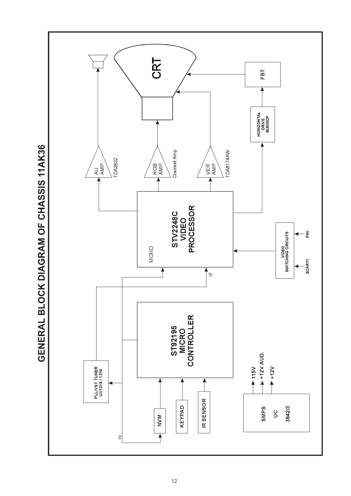
11AK36
12
11AK36-A15
11AK36A8
11AK36-S3
11AK37
22
11AK37-10
11AK37 chassis
11AK41
21
11AK44
11ak44e
11AK45
11AK45 chassis / 11AK45-B5 chassis / 11AK45B5-3 chassis
11AK46
12
11AK46 DVD
2
11AK49
2
11AK52
2
11ak52-b2
11ak52-b4
11AK53
11AK56-4
11AK57
11AK58
11BL37-2
11DF41J-5
11DMP01
11DMP01-3
11DMP02
11DMP2
11DMP3
11FAV116-1
11FAV19A4
11FAV46-13
11FAV46-15
11HP19S
11IR11-3
11LD50-3
11 MB 33
11PIP30N-2
11PIP45-P3
11PIP49-1
11PIP49A-1
11RT45-1
11SB102-2
11SB103-5
11SB106
11SB107-8
11SB117-2
11SB16-3
11SB18-3
11SB19-2
11SBW01-1
10110892
Loading...
Loading...
Nothing found
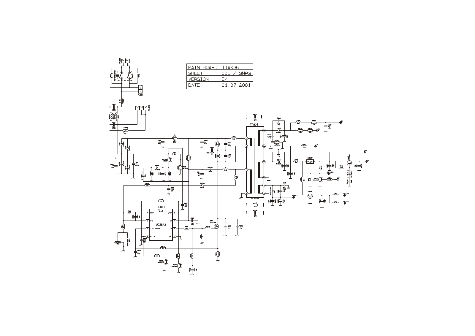
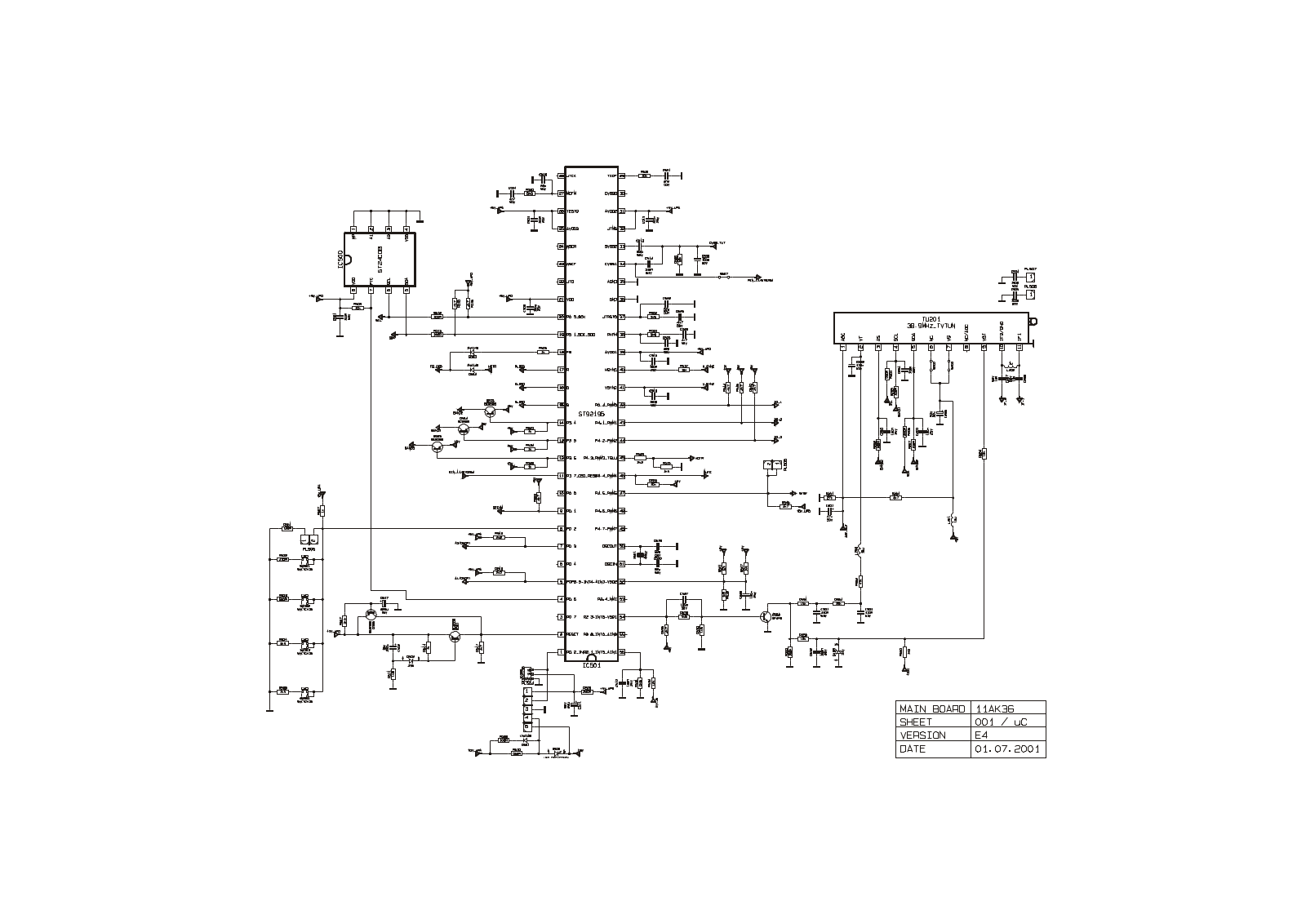
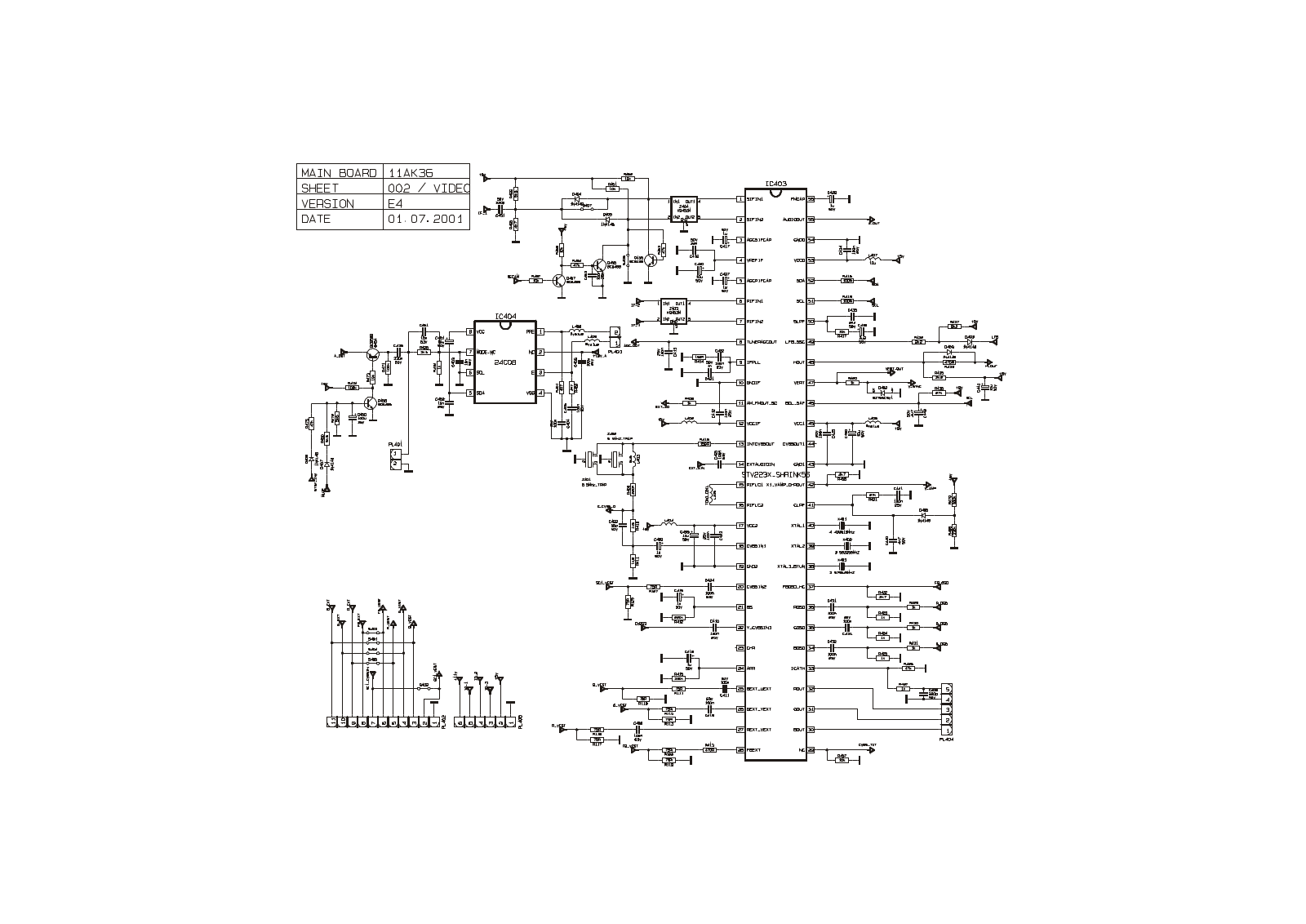
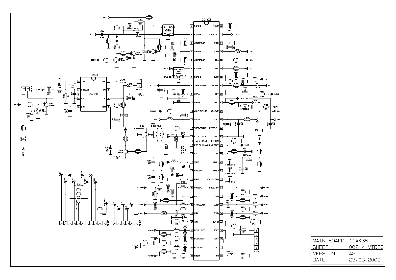
11AK36
Circuit
6 pgs
487.43 Kb
0
Circuit
6 pgs
805.07 Kb
0
Schematics
1 pgs
139.66 Kb
0
Schematics
1 pgs
37.7 Kb
0
Schematics crt
1 pgs
32.26 Kb
0
Schematics deflection
1 pgs
60.87 Kb
0
Schematics smps
1 pgs
62.35 Kb
0
Schematics ucontroller
1 pgs
102.58 Kb
0
Schematics video audio
1 pgs
107.63 Kb
0
Schematics video processor
1 pgs
113.3 Kb
0
Service Manual
27 pgs
1.52 Mb
0
Service Manual
6 pgs
410.19 Kb
0
Table of contents
Loading...
VESTEL 11AK36 Service Manual
...
VESTEL Service Manual
Download
Specifications and Main Features
Frequently Asked Questions
User Manual
Download
Loading...
+
hidden pages
Unhide
You need points to download manuals.
1 point = 1 manual.
You can buy points or you can get point for every manual you upload.
Buy points
Upload your manuals
 Loading...