

Page 1
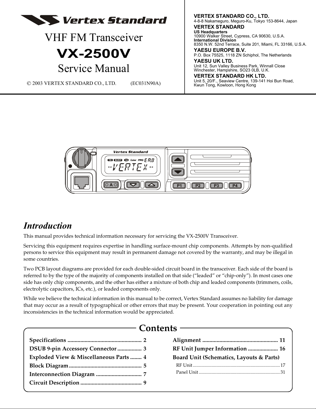
VHF FM Transceiver
VX-2500V
Service Manual
2003 VERTEX STANDARD CO., LTD. (EC031N90A)
©
VERTEX STANDARD CO., LTD.
4-8-8 Nakameguro, Meguro-Ku, Tokyo 153-8644, Japan
VERTEX STANDARD
US Headquarters
10900 Walker Street, Cypress, CA 90630, U.S.A.
International Division
8350 N.W. 52nd Terrace, Suite 201, Miami, FL 33166, U.S.A.
YAESU EUROPE B.V.
P.O. Box 75525, 1118 ZN Schiphol, The Netherlands
YAESU UK LTD.
Unit 12, Sun Valley Business Park, Winnall Close
Winchester, Hampshire, SO23 0LB, U.K.
VERTEX STANDARD HK LTD.
Unit 5, 20/F., Seaview Centre, 139-141 Hoi Bun Road,
Kwun Tong, Kowloon, Hong Kong
Introduction
This manual provides technical information necessary for servicing the VX-2500V Transceiver.
Servicing this equipment requires expertise in handling surface-mount chip components. Attempts by non-qualified
persons to service this equipment may result in permanent damage not covered by the warranty, and may be illegal in
some countries.
Two PCB layout diagrams are provided for each double-sided circuit board in the transceiver. Each side of thr board is
referred to by the type of the majority of components installed on that side (“leaded” or “chip-only”). In most cases one
side has only chip components, and the other has either a mixture of both chip and leaded components (trimmers, coils,
electrolytic capacitors, ICs, etc.), or leaded components only.
While we believe the technical information in this manual to be correct, Vertex Standard assumes no liability for damage
that may occur as a result of typographical or other errors that may be present. Your cooperation in pointing out any
inconsistencies in the technical information would be appreciated.
Contents
Specifications .................................................... 2
DSUB 9-pin Accessory Connector ................. 3
Exploded View & Miscellaneous Parts ........ 4
Block Diagram................................................... 5
Interconnection Diagram ................................ 7
Circuit Description ........................................... 9
Alignment ..................................................... 11
RF Unit Jumper Information ..................... 16
Board Unit (Schematics, Layouts & Parts)
RF Unit ..........................................................................17
Panel Unit ..................................................................... 31
1
Page 2
Specifications
General
Frequency range: 134-160 MHz (Type A)
148-174 MHz (Type C)
Number of Systems: 32
Number of Groups: 250
Number of Channels : 250 channels (Conventional)
640 channels (Trunking)
PLL Steps: 5.0 kHz/6.25kHz
Power Supply Voltage: 13.8V DC ±15 %
Channel Spacing: 12.5 / 25.0 kHz
Current Consumption (Approx.): TX: 6 A
RX: 700 mA
STBY: 250 mA
Operating Temperature range: –22 °F to 140 °F (–30 °C to +60 °C)
Frequency Stability: Better than ±2.5 ppm
RF Input-Output Impedance: 50 ohms
Audio Output Impedance: 4 ohms
Dimensions: 6.3 x 1.6 x 4.3 inch (160 x 40 x 110 mm)
Weight (Approx.): 1.87 lb (0.85 kg)
Receiver (Typical Values)
Circuit type: Double conversion Super-heterodyne
Sensitivity: 0.25 uV (12 dB SINAD)
Adjacent Channel Selectivity: 80/70 dB
Intermodulation: 75 dB
Spurious and Image Rejection: 90 dB
Audio Output: 4 W @ 4 ohms 5% THD
Audio Distortion: <3 % @1 kHz
Transmitter (Typical Values)
Power Output: 25 W (low: 5W)
Modulation: 16K0F3E, 11K0F3E
Max Deviation: 5.0/2.5 kHz
Conducted Spurious Emission: 70 dB below carrier
Audio Distortion: <3 % @ 1 kHz
Microphone type: Dynamic
Microphone impedance: 600 ohms
2
Page 3
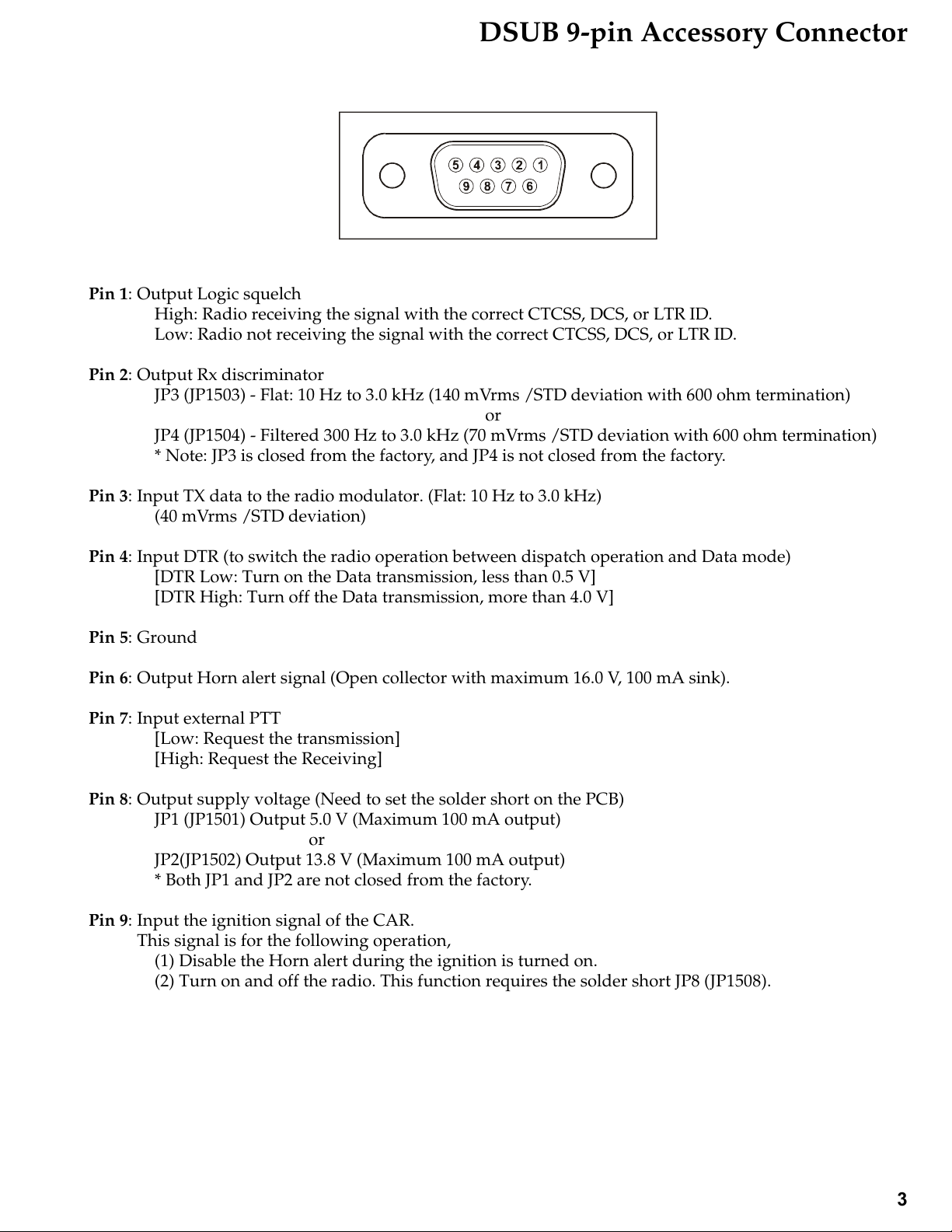
Pin 1: Output Logic squelch
High: Radio receiving the signal with the correct CTCSS, DCS, or LTR ID.
Low: Radio not receiving the signal with the correct CTCSS, DCS, or LTR ID.
Pin 2: Output Rx discriminator
JP3 (JP1503) - Flat: 10 Hz to 3.0 kHz (140 mVrms / STD deviation with 600 ohm termination)
JP4 (JP1504) - Filtered 300 Hz to 3.0 kHz (70 mVrms / STD deviation with 600 ohm termination)
* Note: JP3 is closed from the factory, and JP4 is not closed from the factory.
DSUB 9-pin Accessory Connector
or
Pin 3: Input TX data to the radio modulator. (Flat: 10 Hz to 3.0 kHz)
(40 mVrms / STD deviation)
Pin 4: Input DTR (to switch the radio operation between dispatch operation and Data mode)
[DTR Low: Turn on the Data transmission, less than 0.5 V]
[DTR High: Turn off the Data transmission, more than 4.0 V]
Pin 5: Ground
Pin 6: Output Horn alert signal (Open collector with maximum 16.0 V, 100 mA sink).
Pin 7: Input external PTT
[Low: Request the transmission]
[High: Request the Receiving]
Pin 8: Output supply voltage (Need to set the solder short on the PCB)
JP1 (JP1501) Output 5.0 V (Maximum 100 mA output)
or
JP2(JP1502) Output 13.8 V (Maximum 100 mA output)
* Both JP1 and JP2 are not closed from the factory.
Pin 9: Input the ignition signal of the CAR.
This signal is for the following operation,
(1) Disable the Horn alert during the ignition is turned on.
(2) Turn on and off the radio. This function requires the solder short JP8 (JP1508).
3
Page 4
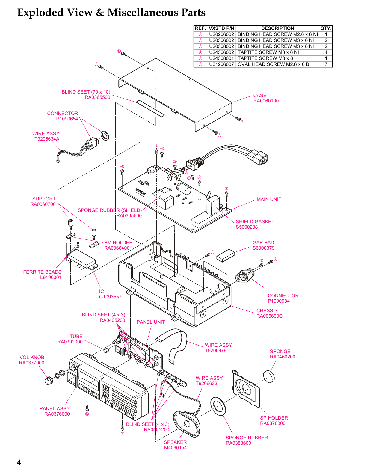
Exploded View & Miscellaneous Parts
CONNECTOR
WIRE ASSY
T9206634A
SUPPORT
RA0060700
†
BLIND SEET (70 x 10)
RA0365500
P1090654
SPONGE RUBBER (SHIELD)
†
„
RA0365500
REF.
VXSTD P/N
•
U20206002
‚
U20306002
ƒ
U20308002
„
U24306002
…
U24308001
†
U31206007
†
…
„
‚
•
‚
„
BINDING HEAD SCREW M2.6 x 6 NI
BINDING HEAD SCREW M3 x 6 NI
BINDING HEAD SCREW M3 x 8 NI
TAPTITE SCREW M3 x 6 NI
TAPTITE SCREW M3 x 8
OVAL HEAD SCREW M2.6 x 6 B
†
„
SHIELD GASKET
S5000238
DESCRIPTION
CASE
RA0060100
MAIN UNIT
QTY.
1
2
2
4
1
7
FERRITE BEADS
L9190001
VOL KNOB
RA0377000
PANEL ASSY
RA0376000
TUBE
RA0392000
PM HOLDER
RA0066400
IC
G1093557
BLIND SEET (4 x 3)
RA0405200
†
PANEL UNIT
BLIND SEET (4 x 3)
†
RA0405200
SPEAKER
M4090154
†
WIRE ASSY
T9206979
WIRE ASSY
T9206633
GAP PAD
S6000379
ƒ
CHASSIS
RA005600C
SP HOLDER
RA0378300
SPONGE RUBBER
RA0383600
ƒ
CONNECTOR
P1090984
SPONGE
RA0460200
4
Page 5
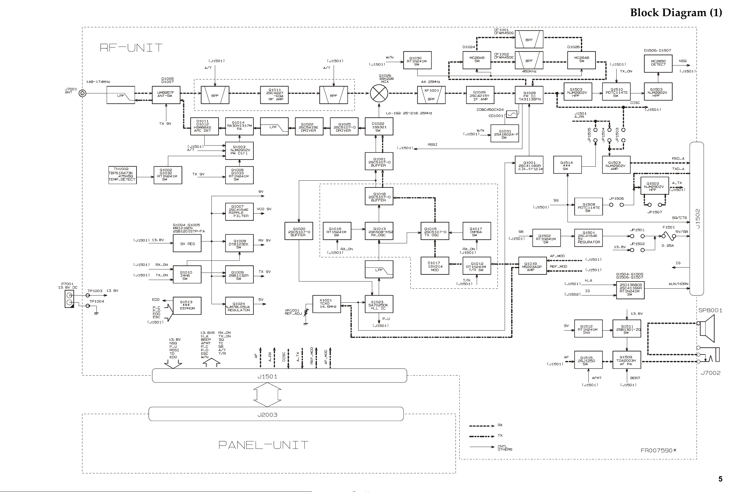
Block Diagram (1)
5
Page 6

Block Diagram (2)
6
Page 7
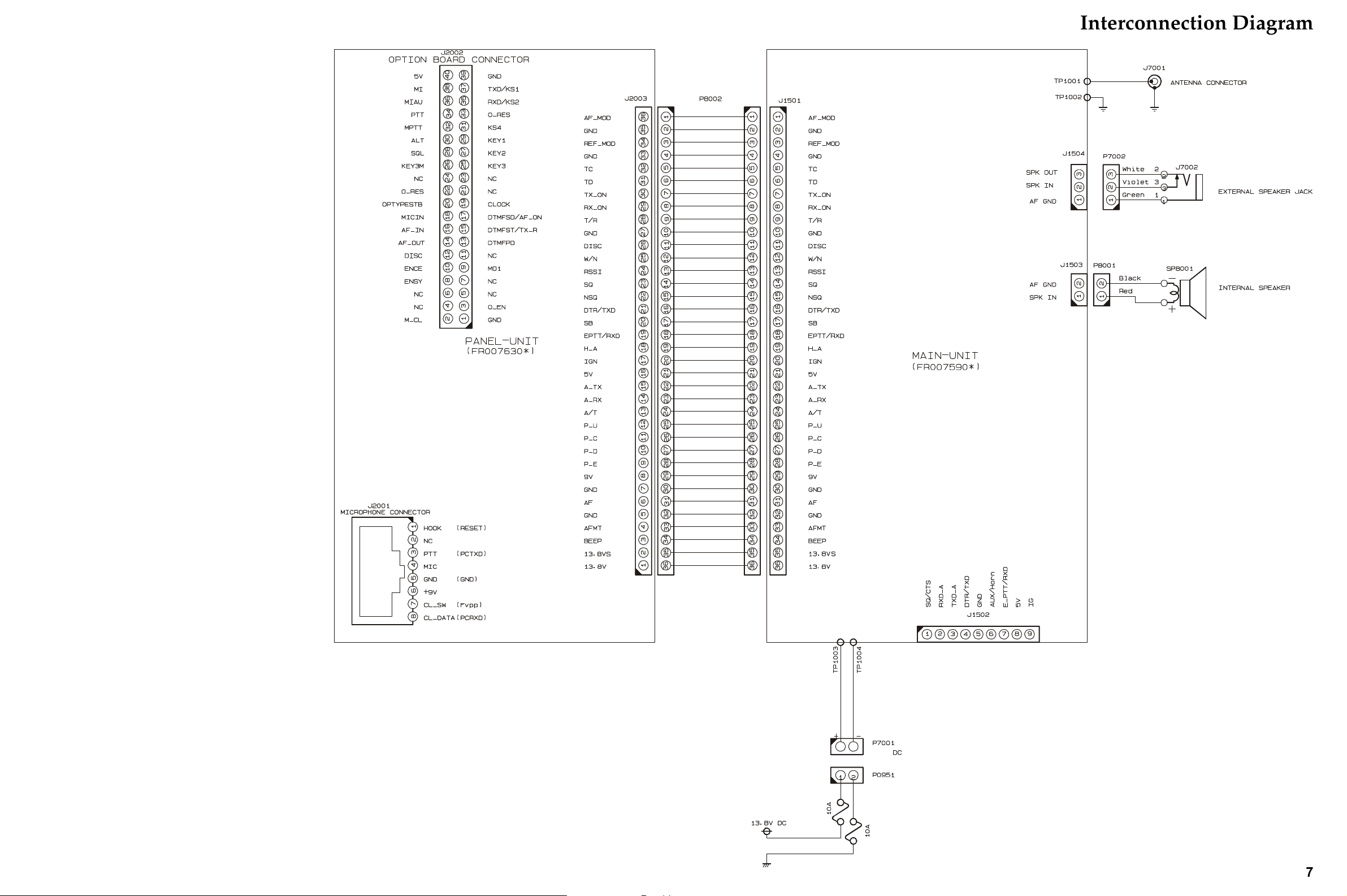
Interconnection Diagram
7
Page 8

Note
8
Page 9
Circuit Description
1. Overview
The VX-2500V is a VHF FM mobile transceiver designed
to operate in the frequency range of 134 to 174MHz.
2. Circuit Configuration by Frequency
The receiver is a double-conversion superheterodyne with
a first intermediate frequency (IF) of 44.25MHz and a sec-
ond IF of 450kHz. Incoming signals from the antenna are
mixed with the local signal from PLL to produce the first
IF of 44.25MHz.
This is then mixed with the 43.8MHz second local oscilla-
tor (using the 14.6MHz reference crystal) output to pro-
duce the 450kHz second IF. This is detected to give the
demodulated signal.
The transmit signal frequency is generated by PLL VCO,
and modulated by the signal from the microphone. It is
then amplified and sent to the antenna.
3. Receive Signal Path
Incoming RF signals from the antenna connector are de-
livered to the RF Unit, and pass through a low-pass filter
(LPF) antenna switching network consisting of coils L1001,
L1002, L1003, L1005, and L1007, capacitors C1004,
C1009,C1016, C1019, and C1025, and antenna switching
diodes D1005 and D1007 (both UM9957F) for delivery to
the receiver front end.
Signals within the frequency range of the transceiver are
then passed through a varactor-tuned bandpass filter con-
sisting of L1008, L1009 before RF amplification by Q1011
(2SC4226).
The amplified RF is then band-pass filtered again by var-
actor-tuned resonators L1019, L1023 to ensure pure in-
band input to 1st mixer Q1026 (3SK228).
Buffered output from the VCO Unit is amplified by Q1021
(2SC5107) and low-pass filtered by L1030/L1032 and
C1184/C1188/C1192, to provide a pure 1st local signal
between 178.25 and 218.25MHz to the 1st mixer.
The 44.25MHz 1st mixer product then passes through dual
monolithic crystal filters XF1001 and XF1002, and is am-
plified by Q1029 (2SC4215Y) and delivered to the input
of the FM IF subsystem IC Q1028 (TA31136FN).
This IC contains the 2nd mixer, 2nd local oscillator, limit-
er amplifier, FM detector, noise amplifier, and squelch
gates.
The 2nd LO in the IF-IC is produced from crystal X1001
(14.600MHz), and the 1st IF is converted to 450kHz by the
2nd mixer and stripped of unwanted components by ce-
ramic filter CF1001 or CF1002. After passing through a
limiter amplifier, the signal is demodulated by the FM
detector CD1001 (CDBC450CX24).
Detected audio from Q1029 is applied to Q2016 (AK2345)
and audio low-pass filter. After volume adjustment by
Q2014 (M62364FP), the audio signal is amplified by the
AF power amplifier Q1509 (TDA2003H) and passed to
speaker jack.
4. Transmit Signal Path
Voice audio from the microphone is delivered via the MIC
(Jack) Unit to the PANEL Unit, after passing through
amplifier Q2022(NJM2902V), Mic gain-volume Q2014
(M62364FP) pre-emphasis Q2015 (NJM2902V), and lim-
iter Q2016 (IDC instantaneous deviation control), is ad-
justed for optimum deviation level and delivered to the
next stage.
Voice input from the microphone and CTCSS are FM-
modulated to the VCO of the synthesizer, while DCS au-
dio is modulated by the reference frequency oscillator of
the synthesizer.
Synthesizer output, after passing through diode switch
D1022 (1SS321), is amplified by driver Q1022
(2SC5415E), Q1025 (2SC5107) and power module Q1014
(RA30H1317M) to obtain full RF output. The RF energy
then passes through antenna switch D1005/D1007 and a
low-pass filter circuit and finally to the antenna connec-
tor.
RF output power from the final amplifier is sampled by
CM coupler and is rectified by D1011, D1012 (both
HSM88AS). The resulting DC is fed through Automatic
Power Controller Q1003 (M5223AGP), Q1002
(2SC4154E), Q1032 (2SC4254E), and TH1003 to trans-
mitter RF amplifier and thus the power output.
Generation of spurious products by the transmitter is min-
imized by the fundamental carrier frequency being equal
to the final transmitting frequency, modulated directly in
the transmit VCO. Additional harmonic suppression is
provided by a low-pass filter consisting of L1002, L1003,
L1005, C1004, C1009, C1016, C1019, and C1025, resulting
in more than 60dB of harmonic suppression prior to de-
livery to the RF energy to the antenna.
5. PLL Frequency Synthesizer
PLL frequency synthesizer consists of the VCO Q1013
(2SK508-K52: RX) and Q1015 (2SC4226-R24: TX), VCO
buffers Q1018, Q1020, Q1021 (all 2SC5107-0), PLL sub-
system IC Q1023 (SA7025DK) and 14.6MHz reference
crystal X1001.
The frequency stability is ±2.5ppm within temperature
range of –30 to +60 degree. The output of the 14.6MHz
reference is applied to pin 8 of the PLL IC.
While receiving, VCO Q1013 oscillates between 178.25 and
218.25MHz according to the transceiver version and the
programmed receiving frequency. The VCO generates
355.75 to 467.75MHz for providing to the first local sig-
nal. In TX, the VCO generates 134 to 174MHz.
9
Page 10

Circuit Description
The output of the VCO is amplified by the Q1020 and rout-
ed to the pin 5 of the PLL IC. Also the output of the VCO
is amplified by the Q1021 and routed first local/Power
Module according to D1022.
The PLL IC consists of a prescaler, fractional divider, ref-
erence divider and phase comparator and charge pump.
This PLL IC is fractional-N type synthesizer and performs
in the 40 or 50 kHz reference signal, which is eighth of the
channel step (5 or 6.25 kHz). The input signal from pin 5
and 8 of the PLL IC is divided down to the 20 kHz and
compared at phase comparator. The pulsed output signal
of the phase comparator is applied to the charge pump
and transformed into DC signal in the loop filter. The DC
signal is applied to the VCO and locked to keep the VCO
frequency constant.
PLL data is output from "DCS_E" (pin100), "CLOCK"
(pin2) and "PLL_E" (pin98) of the microprocessor Q2013.
The data are input to PLL IC when the channel is changed
or when transmission is changed to reception and vice
versa. A PLL lock condition is always monitored by the
pin20 of the Q2013. When the PLL is unlocked, the UL
goes low.
6. Miscellaneous Circuits
6-1 DCS/LTR Demodulator
DCS signals are demodulated on the PANEL-UNIT, It is
demodulated by Q2116 (AK2345), amplifier Q2015, and
comparator Q2021.
6-2 CTCSS encoder/decoder
The CTCSS code is generation and encoding by CTCSS
encoder/decoder IC Q2016 (AK2345).
7. Power Supply Circuits
7-1 All 13.8V
13.8V is always supplied to Power AMP Q1014
(RA30H4452M). Switched 13.8V is supplied to AF Power
AMP Q1509 (TDA2003H) and 9V Regulator Q1004
(MM1216EN) and Q1005 (2SB1201STP).
7-2 All 9V
9V regulated from 13.8V by Q1004 (MM1216EN) and
Q1005 (2SB1201STP).
7-3 VCO 9V
9V is filtered by Ripple Filter and is supplied to VCO Os-
cillator Q1013 (2SK508-K52), Q1015 (2SC5107-O), and
VCO BUFFER AMP Q1015 (2SC5107-O).
7-4 5V (RF-UNIT)
5V in RF-UNIT is regulated by REGULATOR IC Q1024
(NJM78L05UA). 5V is supplied to PLL IC Q1023
(SA7025DK), FM IC Q1028 (TA31136FN), and Reference
Oscillator Q1027 (23C4116GR).
7-5 TX 9V
TX 9V is active on transmit. TX 9V is supplied to ANT SW
D1005, D1007 (UM9957F) and TX DRIVER Q1022
(2SC5415E), Q1025 (2SC5107-O).
7-6 RX 9V
RX 9V is active on receive. RX 9V is supplied to RX RF
AMP Q1026 (3SK228) and MIXER Q1011 (2SC4227-R34).
7-7 5V (RF-UNIT)
9V from RF-UNIT is regulated to 5V by REGULATOR IC
Q2006 (NJM78L05UA) in PANEL-UNIT.
6-3 MPU
Operation is controlled by 8-bit MPU IC Q2013
(LC87F72C8A). The system clock uses a 3.6864MHz crys-
tal for a time base. IC Q2003 (S-80735SN) resets the MPU
when the power is on, and monitors the voltage of the
regulated 5V power supply line.
6-4 DCS/LTR Encorder
The DCS code is generation and encoding by MPU IC
Q2013 (LC87F72C8A). It is filtered by Q2021 (NJM2902V)
and adjusted the level by Q2014 (M62364FP).
6-5 Compandor
The Compandor is active when Pin90 of Q2013
(LC87F72C8A) is “High”. When the Compandor is ac-
tive, MIC Audio is compressed, and detected audio is ex-
panded by Q2017 (LA8630M).
10
Page 11
Alignment
Introduction
The VX-2500V is carefully aligned at the factory for the
specified performance across the frequency range speci-
fied for each version. Realignment should therefore not
be necessary except in the event of a component failure,
or altering version type. All component replacement and
service should be performed only by an authorized Ver-
tex Standard representative,or the warranty policy may
be void.
The following procedures cover the sometimes critical and
tedious adjustments that are not normally required once
the transceiver has left the factory. However, if damage
occurs and some parts subsequently are placed, realign-
ment may be required. If a sudden problem occurs dur-
ing normal operation, it is likely due to component fail-
ure; realignment should not be done until after the faulty
component has been replaced.
We recommend that servicing be performed only by au-
thorized Vertex Standard service technicians who are ex-
perienced with the circuitry and fully equipped for repair
and alignment. Therefore, if a fault is suspected, contact
the dealer from whom the transceiver was purchased for
instructions regarding repair. Authorized Vertex Standard
service technicians realign all circuits and make complete
performance checks to ensure compliance with factory
specifications after replacing any faulty components.
Those who do undertake any of the following alignments
are cautioned to proceed at their own risk. Problems
caused by unauthorized attempts at realignment are not
covered by the warranty policy. Also, Vertex Standard
reserves the right to change circuits and alignment proce-
dures in the interest of improved performance, without
notifying owners.
Under no circumstances should any alignment be attempt-
ed unless the normal function and operation of the trans-
ceiver are clearly understood, the cause of the malfunc-
tion has been clearly pinpointed and any faulty compo-
nents replaced, and realignment determined to be abso-
lutely necessary.
The following test equipment (and thorough familiarity
with its correct use) is necessary for complete realignment.
Correction of problems caused by misalignment result-
ing from use of improper test equipment is not covered
under the warranty policy. While most steps do not re-
quire all of the equipment listed, the interactions of some
adjustments may require that more complex adjustments
be performed afterwards.
Required Test Equipment
r RF Signal Generator with calibrated output level
at 500MHz
r Deviation Meter (linear detector)
r In-line Wattmeter with 5% accuracy at 1000MHz
r 50W RF Dummy Load with power rating 100W
at 500MHz
r 4W AF Dummy Load
r Regulated DC Power Supply (standard 13.8V
DC, 15A)
r Frequency Counter with 0.1ppm accuracy at
500MHz
r AC Voltmeter
r DC Voltmeter
r VHF Sampling Coupler
r IBM PC/compatible Computer
r Oscilloscope
r Vertex Standard VPL-1 Connection Cable &
Alignment program
Alignment Preparation & Precautions
A 50W RF Dummy Load and in-line wattmeter must be
connected to the main antenna jack in all procedures that
call for transmission, except where specified otherwise.
Correct alignment is not possible with an antenna.
After completing one step, read the following step to de-
termine whether the same test equipment will be required.
If not, remove the test equipment (except dummy load
and wattmeter, in connected) before proceeding.
Correct alignment requires that the ambient temperature
be the same as that of the transceiver and test equipment,
and that this temperature be held constant between 68°F
and 86°F (20°C ~ 30°C). When the transceiver is brought
into the shop from hot or cold air, it should be allowed
time to come to room temperature before alignment.
Whenever possible, alignments should be made with os-
cillator shields and circuit boards firmly affixed in place.
Also, the test equipment must be thoroughly warmed up
before beginning.
Note: Signal levels in dB referred to in the alignment pro-
cedure are based on 0dBm EMF = 0.5mV.
Do not attempt to perform only a single step unless it is
clearly isolated electrically from all other steps. Have all
test equipment ready before beginning, and follow all of
the steps in a section in the order presented.
11
Page 12
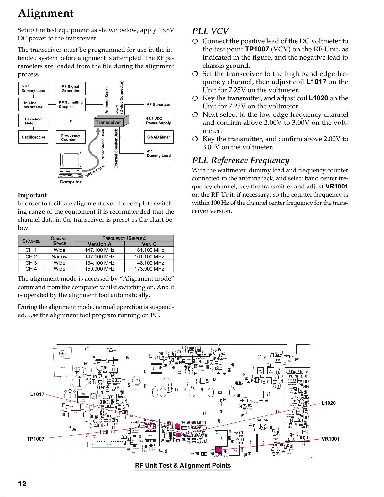
Alignment
Transceiver
Setup the test equipment as shown below, apply 13.8V
DC power to the transceiver.
The transceiver must be programmed for use in the in-
tended system before alignment is attempted. The RF pa-
rameters are loaded from the file during the alignment
process.
Important
In order to facilitate alignment over the complete switch-
ing range of the equipment it is recommended that the
channel data in the transceiver is preset as the chart be-
low.
CHANNEL
CH 1
CH 2
CH 3
CH 4
CHANNEL
SPACE
Wide
Narrow
Wide
Wide
FREQUENCY (SIMPLEX
Version A
147.100 MHz
147.100 MHz
134.100 MHz
159.900 MHz
)
Ver. C
161.100 MHz
161.100 MHz
148.100 MHz
173.900 MHz
The alignment mode is accessed by “Alignment mode”
command from the computer whilst switching on. And it
is operated by the alignment tool automatically.
PLL VCV
Connect the positive lead of the DC voltmeter to
¦
the test point TP1007 (VCV) on the RF-Unit, as
indicated in the figure, and the negative lead to
chassis ground.
Set the transceiver to the high band edge fre-
¦
quency channel, then adjust coil L1017 on the
Unit for 7.25V on the voltmeter.
Key the transmitter, and adjust coil L1020 on the
¦
Unit for 7.25V on the voltmeter.
Next select to the low edge frequency channel
¦
and confirm above 2.00V to 3.00V on the volt-
meter.
Key the transmitter, and confirm above 2.00V to
¦
3.00V on the voltmeter.
PLL Reference Frequency
With the wattmeter, dummy load and frequency counter
connected to the antenna jack, and select band center fre-
quency channel, key the transmitter and adjust VR1001
on the RF-Unit, if necessary, so the counter frequency is
within 100 Hz of the channel center frequency for the trans-
ceiver version.
During the alignment mode, normal operation is suspend-
ed. Use the alignment tool program running on PC.
L1017
TP1007
12
L1020
VR1001
RF Unit Test & Alignment Points
Page 13
Alignment
The alignment tool outline
Installation the tool
This alignment tool consists, MS-DOS based, only one ex-
ecute file “svc47.exe.“ You make a directly as you think
fit, and copy this file. That is all of the installation pro-
cess.
Boot the tool
Change directly and input in command line, “svc47 [en-
ter],“ and boot the alignment tool.
Preparation
Setup the test equipment as “Alignment Preparation &
Precautions.”
Set the RF Ch. List to Table 1 on the CE47 Clone editor
software.
Enter to the alignment mode
To enter the alignment mode, press “[0] Alignment Mode”
on the personal computer Key board. You turn off the
power of the transceiver, and turn on the transceiver. If
entry succeed,the alignment tool display as follows.
[0]Common TX
[1]Common RX
Action of the switches
When the transceiver is in alignment mode, the action of
[PTT], [MON], [UP], and [DOWN] is ignored. All of the
action is remote controlled by PC.
Menu of the tool
[0] Common TX
- [0] Tx Power High
This parameter is used to align TX High power (25W).
Press [Enter] on “[0] Tx Power High” to align
¦
TX High power.
Select the Channel “1“ in alignment range.
¦
Press the [Space] key on the keyboard to acti-
¦
vate the transmitter.
Press the [UP] or [DWN] key, as needed, to set
¦
the power output to the following specification,
as indicated on the external wattmeter.
Tx Power High: 25 W (±0.5W)
When the 25 Watt level is attained, press [Enter]
¦
to lock in the new data.
- [1] Tx Power Low
This parameter is used to align TX Low power (5W).
Press [Enter] on “[1] Tx Power Low” to align TX
¦
Low power.
Select the Channel “1“ in alignment range.
¦
Press the [Space] key on the keyboard to acti-
¦
vate the transmitter.
Press the [UP] or [DWN] key, as needed, to set
¦
the power output to the following specification,
as indicated on the external wattmeter.
Tx Power Low: 5 W (±0.1W)
When the 5 Watt level is attained, press [Enter]
¦
to lock in the new data.
- [2] VCO Deviation
This parameter is used to align the VCO Deviation.
Press [Enter] on “[2] VCO Deviation” to align
¦
VCO Deviation.
Select the Channel “1“ in alignment range.
¦
Adjust the AF generator output level to
¦
38mVrms (–26dBm) at 2 kHz to the pin 3 of the
J1502 (D-sub 9pin ).
Press the [Space] key on the keyboard to acti-
¦
vate the transmitter.
Press the [UP] or [DWN] key, as needed, to set
¦
the VCO Deviation (Wide) to the following speci-
fication, as indicated on the deviation meter.
When the desired deviation level is attained,
¦
press [Enter] to lock in the new data.
Select the Channel 2, and set the VCO Deviation
¦
(Narrow), same as Channel “1.“
VCO Deviation (Wide): 3.0 kHz (±0.1 kHz)
VCO Deviation (Narrow): 1.5 kHz (±0.1 kHz)
13
Page 14

Alignment
- [3] REF Deviation
This parameter is used to align the REF Deviation.
Press [Enter] on “[3] REF Deviation” to align REF
¦
Deviation.
Select the Channel “1“ in alignment range.
¦
Adjust the AF generator output level to
¦
776mVrms(0dBm) at 300Hz to the pin 3 of the
J1502.
Press the [Space] key on the keyboard to acti-
¦
vate the transmitter.
Press the [UP] or [DWN] key, as needed, to set
¦
the modulation wave as follows.
Press [Enter] to lock in the new data.
¦
Select the Channel “2,“ and set the modulation
¦
wave, same as Channel “1.“
OK NG NG
- [4] CTCSS Deviation
This parameter is used to align the CTCSS deviation.
Press [Enter] on “[4] CTCSS Deviation” to align
¦
CTCSS Deviation.
Select the Channel “1“ in alignment range.
¦
Press the [Space] on the keyboard to activate the
¦
transmitter, and injects a CTCSS test tone.
Press the [UP]/[DWN] key, as need, to set the
¦
CTCSS Deviation (Wide) to the following speci-
fication.
Press [Enter] to lock in the new data.
¦
Select the Channel “2,“ and set the CTCSS De-
¦
viation (Narrow), same as Channel “1.“
CTCSS Deviation (Wide): 0.70 kHz (±0.1 kHz)
CTCSS Deviation (Narrow): 0.35 kHz (±0.1 kHz)
- [5] DCS Deviation
This parameter is used to align the DCS deviation.
Press [Enter] on “[5] DCS Deviation” to align
¦
DCS Deviation.
Select the Channel “1“ in alignment range.
¦
Press the [Space] key on the keyboard to acti-
¦
vate the transmitter, and injects a DCS test tone.
Press the [UP] or [DWN] key, as needed, to set
¦
the DCS deviation (Wide) to the following speci-
fication.
Press [Enter] to lock in the new data.
¦
Select the Channel “2,“ and set the DCS devia-
¦
tion (Narrow), same as Channel “1.“
DCS Deviation (Wide): 0.60 kHz (±0.1 kHz)
DCS Deviation (Narrow): 0.30 kHz (±0.1kHz)
The actual DCS deviation will increase around
¦
20% based on the above alignment as follows,
Actual DCS Deviation (Wide): 0.70 kHz
Actual DCS Deviation (Narrow): 0.35 kHz
- [6] LTR Deviation
This parameter is used to align the LTR deviation.
Press [Enter] on “[6] LTR Deviation “ to align
¦
LTR Deviation.
Select the Channel “1“ in alignment range.
¦
Press the [Space] key on the keyboard to acti-
¦
vate the transmitter, and injects a LTR test tone.
Press the [UP] or [DWN] key, as needed, to set
¦
the LTR Deviation (Wide) to the following speci-
fication.
Press [Enter] to lock in the new data.
¦
Select the Channel “2,“ and set the LTR devia-
¦
tion (Narrow), same as Channel “1.“
LTR Deviation (Wide): 0.80 kHz (±0.1 kHz)
LTR Deviation (Narrow): 0.60 kHz (±0.1 kHz)
The actual LTR deviation will increase around
¦
20% based on the above alignment as follows,
Actual LTR Deviation (Wide): 1.00 kHz
Actual LTR Deviation (Narrow): 0.70 kHz
14
Page 15

[1] Common RX
- [0] Tight NSQL
This parameter is used to align the noise level in squelch
Tight. It adjusts this alignment RX Tuning after ending.
Select the MID frequency channel in alignment
¦
range.
Set the SG output level to 0dBm EMF, and obey
¦
the message.
- [1] Threshold NSQL
This parameter is used to align the noise level in squelch
Threshold. It adjusts this alignment RX Tuning after end-
ing.
Select the MID frequency channel in alignment
¦
range.
Set the SG output level to –7dBm EMF, and obey
¦
the message.
- [2] RX Tune
This parameter is used to align RX Tune.
Select the MID frequency channel in alignment
¦
range.
Set the SG output level to –6dBm EMF.
¦
Pressing the [DWN] key, reduce the RX Tune
¦
Level and set the SINAD above 12dB.
Alignment
15
Page 16

RF Unit Jumper Information
JP1501 (JP1): Determine the output supply voltage at pin 8 of DSUB 9-pin Accessory Connector.
Close: +5.0 V (Maximum 100 mA)
Open: No Action
JP1502 (JP2): Determine the output supply voltage at pin 8 of DSUB 9-pin Accessory Connector.
Close: +13.8 V (Maximum 100 mA)
Open: No Action
JP1503 (JP3): Determine the Rx discriminator output characteristic at pin 2 of DSUB 9-pin Accessory Connec-
tor.
Close: Flat 10 Hz to 3.0 kHz (140 mVrms / STD deviation with 600 ohm termination)
Open: No Action
JP1504 (JP4): Determine the Rx discriminator output characteristic at pin 2 of DSUB 9-pin Accessory Connec-
tor.
Close: Filtered 300 Hz to 3.0 kHz (70 mVrms / STD deviation with 600 ohm termination)
Open: No Action
JP1505 (JP5): No Action (Spare Jumper).
JP1506 (JP6): Define whether the TX Data Input at pin 3 of DSUB 9-pin Accessory Connector shall be "on" or
"off" according to the external PTT Input signal signal (pin 7 of DSUB 9-pin Accessory Connec-
tor).
Close: on (Enabled)
Open: off (Disabled)
JP1507 (JP7): Determine the TX Data Input level at pin 3 of DSUB 9-pin Accessory Connector.
Close: 400 mVrms / STD deviation with 600 ohm termination
Open: 40 mVrms / STD deviation with 600 ohm termination
JP1508 (JP8): Define whether the Transceiver's power shall be "on" or "off" according to the Ignition Signal
Input (pin 9 of DSUB 9-pin Accessory Connector).
Close: Turn the transceiver on when the Ignition Signal Input (pin 9 of DSUB 9-pin Accessory
Connector) is turned to "High" while the VOL/PWR knob is set to the "ON" position (out
of the click-stop position).
Open: No Action
16
Page 17

RX: 0 V
TX: 1.6 V
HIGH POWER: 0 V
LOW POWER: 0 V
RX: 0 V
TX: 1.9 V
RF Unit
Circuit Diagram (1)
WIDE: 0 V
NARROW: 5.0 V
HIGH POWER: 2.6 V
LOW POWER: 1.0 V
HIGH POWER: 3.3 V
LOW POWER: 2.5 V
4.1 V
TX: 5.5 V
9.0 V
RX: 0 V
HIGH POWER: 2.6 V
LOW POWER: 1.0 V
RX: 0 V
TX: 8.9 V
8.1 V
7.5 V
RX: 0 V
TX: 1.7 V
RX: 1.0 V
TX: 1.7 V
RX: 0 V
TX: 1.7 V
RX: 0 V
TX: 7.6 V
6.9 V
RX: 4.6 V
TX: 4.6 V
2.4 V
RX: 0 V
TX: 1.5 V
0.7 V
RX: 0 V
TX: 8.1 V
0.4 V
8.0 V
4.9 V
4.7 V
3.8 V
RX: 0 V
TX: 4.2 V
RX: 0 V
TX: 3.0 V
RX: 0 V
TX: 2.6 V
1.7 V
3.0 V
3.9 V
0.6 V
RX: 4.3 V
TX: 0 V
WIDE: 1.8 V
NARROW: 1.6 V
WIDE: 2.3 V
NARROW: 0 V
WIDE: 0.4 V
NARROW: 2.2 V
4.7 V
0.8 ~ 2.3 V
1.0 V
5.0 V
0 V
4.6 V
WIDE: 0.4 V
NARROW: 2.2 V
2.5 V
5.0 V
1.1 V
4.1 V
WIDE: 1.8 V
NARROW: 1.6 V
1.2 ~ 4.2 V
0.7 V
3.8 V
3.8 V
3.8 V
3.8 V
3.8 V
RX: 8.9 V
TX: 8.2 V
2.0 ~ 7.0 V
RX: 0 V
TX: 5.0 V
RX: 0 V
TX: 8.9 V
RX: 8.8 V
TX: 0 V
RX: 5.0 V
TX: 0 V
RX: 0 V
TX: 0.4 V
RX: 7.8 V
TX: 0 V
RX: 2.3 V
TX: 0 V
RX: 4.6 V
TX: 0 V
RX: 3.8 V
TX: 0 V
4.7 V
0 V
RX: 8.7 V
TX: 0 V
RX: 0.4 V
TX: 0 V
8.4 V
0.7 V
17
Page 18

RF Unit
Circuit Diagram (2)
4.8 V
0.7 V
2.2 V
1.3 V
1.2 V
RX WIDE: 0.2 ~ 3.8 V
RX NARROW: 0.2 ~ 3.5 V
RX WIDE: 0.3 ~ 5.6 V
RX NARROW: 0.3 ~ 5.1 V
3.7 V
TX: 0.2 V
TX: 0.3 V
3.7 V
RX WIDE: 0.8 ~ 3.8 V
RX NARROW: 0.8 ~ 3.1 V
TX: 0.8 V
1.2 V
0.7 V
3.7 V
8.5 V
3.7 V
RX: 0.3 V
TX: 0 V
3.7 V
3.7 V
18
5.3 V
5.8 V
3.7 V
HORN OFF: 0 V
HORN ACTIVE: 8.9 V
HORN OFF: 0 V
HORN ACTIVE: 0.6 V
3.7 V
HORN OFF: 0 V
HORN ACTIVE: 5.0 V
HORN OFF: 8.9 V
HORN ACTIVE: 8.3 V
HORN OFF: 8.9 V
HORN ACTIVE: 0 V
HORN OFF: 0 V
HORN ACTIVE: 4.2 V
BUSY: 5.0 V
MUTE: 0 V
HORN OFF: 10.0 V
HORN ACTIVE: 0 V
0.8 V
BUSY: 4.2 V
MUTE: 0 V
BUSY: 0 V
MUTE: 13.7 V
0.9 V
0.8 V
13.8 V
1.3 V
1.6 V
0 V
13.1 V
7.3 V
Page 19

RF Unit
Parts Layout (Side A)
A CB ED GF H
1
2
3
4
TDA2003H
(Q1509)
SA7025DK
(Q1023)
NJM2902V
(Q1003, 1503)
M5223
(Q1019)
2SA1602A (MF)
(Q1505)
2SB1301 (ZQ)
(Q1511)
2SD1368CB (CB)
(Q1504)
2SC4154 (LE)
(Q1501)
2SC4226 (R22)
(Q1011, 1015)
2SC5107 (MF0)
(Q1518)
2SK508 (K52)
(Q1013)
3SK228 (XR)
(Q1026)
IMH6A (H6)
(Q1017)
RT1N241M (N2)
(Q1002, 1006,
1016, 1032, 1033,
1034, 1035, 1502,
1506, 1507, 1512,
1518)
HSM88AS (C1)
(D1011, 1012)
MC2850 (A7)
(D1506, 1507)
19
Page 20

RF Unit
Parts Layout (Side B)
a
b
c
d
e
f h
g
1
1SS321 (F9)
(D1022)
MC2848 (A6)
(D1024, 1026)
2
MC2850 (A7)
(D1501, 1502, 1503)
RT1N241M (N2)
(Q1012, 1030,
3
4
1516, 1517)
PDTC114TE (24)
(Q1508, 1510)
20
RA30H1317M
(Q1014)
TA31136FN
(Q1028)
2SB1201S
(Q1005)
2SA1602A (MF)
(Q1031)
2SB1132 (BA)
(Q1009)
2SC4116 (LG)
(Q1001)
2SC4154 (LE)
(Q1007, 1519)
2SC4215Y (QY)
(Q1029)
2SC5107 (MFO)
(Q1020, 1021, 1025)
2SC5415E (EA)
(Q1022)
2SJ125D (JD)
(Q1515)
DTB123EK (F12)
(Q1008)
IMH6A (H6)
(Q1010)
MM1216ENRE
(Q1004)
NJM78L05
(Q1024)
Page 21

RF Unit
Parts List
REF DESCRIPTION VALUE V/W TOL. MFR'S DESIG VXSTD P/N VERS.
PCB with Component CB1724001
Printed Circuit Board AC031N000 FR0075900 1-
C 1001 CHIP CAP. 470pF 50V CH GRM39CH471J50PT K22174249 1- A G3
C 1002 CHIP CAP. 0.001uF 630V R GHM1030R102K630PT K22281801 1- A G1
C 1003 CHIP CAP. 220pF 50V CH GRM39CH221J50PT K22174243 1- A D1
C 1004 CHIP CAP. 15pF 200V CH GRM40CH150J200PT K22230218 1- A G1
C 1005 CHIP CAP. 0.1uF 25V B GRM40B104M25PT K22140811 1- A E1
C 1006 CHIP CAP. 15pF 50V CH GRM39CH150J50PT K22174215 1- A G2
C 1007 CHIP CAP. 15pF 50V CH GRM39CH150J50PT K22174215 1- A G1
C 1008 CHIP CAP. 0.001uF 50V B GRM39B102K50PT K22174821 1- B g3
C 1009 CHIP CAP. 27pF 200V CH GRM40CH270J200PT K22230221 1- A G1
C 1011 CHIP CAP. 0.01uF 50V B GRM39B103M50PT K22174823 1- A E1
C 1012 CHIP TA.CAP. 6.8uF 6.3V TEMSVA0J685M-8R K78080025 1- A C3
C 1013 CHIP TA.CAP. 6.8uF 6.3V TEMSVA0J685M-8R K78080025 1- A B3
C 1014 AL.ELECTRO.CAP. 10uF 16V RV2-16V100MB55-R K48120014 1- A B2
C 1015 CHIP CAP. 12pF 50V CH GRM39CH120J50PT K22174213 1- A G1
C 1016 CHIP CAP. 9pF 50V CH GRM39CH090D50PT K22174210 1- A F1
C 1017 CHIP CAP. 0.001uF 50V B GRM39B102K50PT K22174821 1- A C1
C 1019 CHIP CAP. 33pF 200V CH GRM40CH330J200PT K22230222 1- A G1
C 1020 CHIP CAP. 10pF 50V CH GRM39CH100D50PT K22174211 1- A G1
C 1021 CHIP CAP. 100pF 50V CH GRM39CH101J50PT K22174235 1- B f1
C 1022 CHIP CAP. 12pF 50V CH GRM39CH120J50PT K22174213 1- A G1
C 1023 CHIP CAP. 0.047uF 16V B GRM39B473K16PT K22124804 1- A D1
C 1025 CHIP CAP. 5pF 200V CH GRM40CH050C200PT K22230207 1- A F1
C 1026 CHIP CAP. 0.001uF 50V B GRM39B102K50PT K22174821 1- A B1
C 1027 AL.ELECTRO.CAP. 3300uF 16V RE3-16V332M 3300UF K40129065 1- A C1
C 1028 CHIP CAP. 15pF 50V CH GRM39CH150J50PT K22174215 1- A G1
C 1029 CHIP CAP. 0.0022uF 50V B GRM39B222K50PT K22174822 1- A D1
C 1030 CHIP CAP. 22pF 50V CH GRM39CH220J50PT K22174219 1- A C4
C 1031 CHIP CAP. 33pF 50V CH GRM39CH330J50PT K22174223 1- A G1
C 1032 CHIP CAP. 0.0047uF 50V B GRM39B472K50PT K22174833 1- A D1
C 1033 CHIP TA.CAP. 47uF 16V TEMSVC1C476M12R K78120057 1- B f1
C 1034 CHIP CAP. 22pF 200V CH GRM40CH220J200PT K22230220 1- A F1
C 1035 CHIP CAP. 0.001uF 50V B GRM39B102K50PT K22174821 1- A D2
C 1036 CHIP CAP. 33pF 50V CH GRM39CH330J50PT K22174223 1- A G1
C 1037 CHIP CAP. 47pF 50V CH GRM39CH470J50PT K22174227 1- A C3
C 1038 CHIP CAP. 470pF 50V CH GRM39CH471J50PT K22174249 1- B c3
C 1039 CHIP CAP. 0.001uF 50V B GRM39B102K50PT K22174821 1- A D1
C 1040 CHIP CAP. 7pF 50V CH GRM39CH070D50PT K22174208 1- A G1
C 1041 CHIP CAP. 2pF 50V CK GRM39CK020C50PT K22174203 1- B b3
C 1042 CHIP CAP. 18pF 50V CH GRM39CH180J50PT K22174217 1- A G1
C 1043 CHIP CAP. 0.001uF 50V B GRM39B102K50PT K22174821 1- A D1
C 1044 CHIP CAP. 12pF 50V CH GRM39CH120J50PT K22174213 1- A G2
C 1046 CHIP CAP. 0.001uF 50V B GRM39B102K50PT K22174821 1- B c3
C 1047 CHIP CAP. 0.001uF 50V B GRM39B102K50PT K22174821 1- A D1
C 1048 CHIP CAP. 47pF 50V CH GRM39CH470J50PT K22174227 1- A G2
C 1049 CHIP CAP. 0.1uF 16V B GRM39B104K16PT K22124805 1- A D1
C 1050 CHIP TA.CAP. 10uF 10V TEMSVA1A106M-8R K78100028 1- B d2
C 1051 CHIP CAP. 470pF 50V CH GRM39CH471J50PT K22174249 1- B b2
C 1052 CHIP CAP. 0.001uF 50V B GRM39B102K50PT K22174821 1- B b2
C 1053 CHIP TA.CAP. 10uF 10V TEMSVA1A106M-8R K78100028 1- B d3
C 1054 CHIP CAP. 0.001uF 50V B GRM39B102K50PT K22174821 1- B d3
C 1055 CHIP CAP. 12pF 50V CH GRM39CH120J50PT K22174213 1- A G2
C 1057 CHIP CAP. 0.01uF 50V B GRM39B103M50PT K22174823 1- A E1
C 1058 CHIP CAP. 470pF 50V CH GRM39CH471J50PT K22174249 1- A D1
C 1059 CHIP CAP. 0.01uF 50V B GRM39B103M50PT K22174823 1- A C2
C 1060 CHIP CAP. 0.001uF 50V B GRM39B102K50PT K22174821 1- B b2
C 1061 CHIP CAP. 0.5pF 50V CK GRM39CK0R5C50PT K22174201 1- B b3
C 1062 CHIP CAP. 470pF 50V CH GRM39CH471J50PT K22174249 1- B d3
C 1063 CHIP CAP. 470pF 50V CH GRM39CH471J50PT K22174249 1- A E1
C 1064 CHIP CAP. 6pF 50V CH GRM39CH060D50PT K22174207 1- A G2
C 1065 CHIP CAP. 0.01uF 50V B GRM39B103M50PT K22174823 1- B c2
C 1066 CHIP CAP. 470pF 50V CH GRM39CH471J50PT K22174249 1- A F2
C 1067 CHIP CAP. 15pF 50V CH GRM39CH150J50PT K22174215 1- A G2
C 1068 CHIP CAP. 470pF 50V CH GRM39CH471J50PT K22174249 1- A F2
C 1069 CHIP CAP. 470pF 50V CH GRM39CH471J50PT K22174249 1- B e2
C 1070 CHIP CAP. 47pF 50V CH GRM39CH470J50PT K22174227 1- A G2
C 1071 CHIP CAP. 470pF 50V CH GRM39CH471J50PT K22174249 1- B b3
C 1072 CHIP CAP. 0.01uF 50V B GRM39B103M50PT K22174823 1- A F2
C 1073 CHIP CAP. 0.001uF 50V B GRM39B102K50PT K22174821 1- B f2
C 1074 CHIP CAP. 470pF 50V CH GRM39CH471J50PT K22174249 1- B f1
C 1075 CHIP CAP. 470pF 50V CH GRM39CH471J50PT K22174249 1- B b2
C 1076 CHIP CAP. 470pF 50V CH GRM39CH471J50PT K22174249 1- B g3
C 1078 CHIP CAP. 470pF 50V CH GRM39CH471J50PT K22174249 1- A F2
C 1079 CHIP CAP. 0.001uF 50V B GRM39B102K50PT K22174821 1- B b2
C 1080 CHIP CAP. 0.001uF 50V B GRM39B102K50PT K22174821 1- B c4
LOT
SIDE
LAY ADR
21
Page 22

RF Unit
Parts List
REF DESCRIPTION VALUE V/W TOL. MFR'S DESIG VXSTD P/N VERS.
C 1081 CHIP CAP. 470pF 50V CH GRM39CH471J50PT K22174249 1- B g3
C 1082 CHIP CAP. 220pF 50V CH GRM39CH221J50PT K22174243 1- A D3
C 1083 CHIP CAP. 470pF 50V CH GRM39CH471J50PT K22174249 1- B g2
C 1084 CHIP CAP. 0.1uF 16V B GRM39B104K16PT K22124805 1- B b2
C 1085 CHIP CAP. 0.001uF 50V B GRM39B102K50PT K22174821 1- A G2
C 1087 CHIP CAP. 0.001uF 50V B GRM39B102K50PT K22174821 1- A F2
C 1088 CHIP CAP. 0.01uF 50V B GRM39B103M50PT K22174823 1- A G2
C 1090 CHIP CAP. 0.1uF 16V B GRM39B104K16PT K22124805 1- A G2
C 1092 CHIP CAP. 0.001uF 50V B GRM39B102K50PT K22174821 1- B e3
C 1093 CHIP CAP. 220pF 50V CH GRM39CH221J50PT K22174243 1- A D4
C 1096 CHIP CAP. 220pF 200V CH GRM40CH221J200PT K22230232 1- A F2
C 1097 CHIP CAP. 0.0022uF 50V B GRM39B222K50PT K22174822 1- A D3
C 1098 CHIP CAP. 0.1uF 16V B GRM39B104K16PT K22124805 1- B e3
C 1100 CHIP CAP. 7pF 50V CH GRM39CH070D50PT K22174208 1- A D3
C 1101 CHIP CAP. 0.001uF 50V B GRM39B102K50PT K22174821 1- A C2
C 1102 CHIP CAP. 1uF 50V B GRM42-2B105K50PT K22175801 1- A E2
C 1103 CHIP CAP. 3pF 50V CJ GRM39CJ030C50PT K22174204 1- B e3
C 1104 CHIP CAP. 0.001uF 50V B GRM39B102K50PT K22174821 1- B e3
C 1105 CHIP CAP. 47pF 50V CH GRM39CH470J50PT K22174227 1- A G2
C 1107 CHIP CAP. 0.001uF 50V B GRM39B102K50PT K22174821 1- A E2
C 1108 CHIP CAP. 470pF 50V CH GRM39CH471J50PT K22174249 1- A F2
C 1109 CHIP CAP. 1pF 50V CK GRM39CK010C50PT K22174202 1- A D3
C 1111 CHIP CAP. 47pF 50V CH GRM39CH470J50PT K22174227 1- A G2
C 1112 CHIP CAP. 0.001uF 50V B GRM39B102K50PT K22174821 1- A E2
C 1113 CHIP CAP. 18pF 50V CH GRM39CH180J50PT K22174217 1- A D3
C 1114 CHIP CAP. 470pF 50V CH GRM39CH471J50PT K22174249 1- A D2
C 1115 FILM CAP. 0.022uF 16V ECHU1C223JB5 K57120011 1- B e3
C 1116 CHIP CAP. 0.001uF 50V B GRM39B102K50PT K22174821 1- B e2
C 1117 CHIP CAP. 7pF 50V CH GRM39CH070D50PT K22174208 1- A G2
C 1118 CHIP CAP. 18pF 50V CH GRM39CH180J50PT K22174217 1- A G2
C 1119 CHIP CAP. 1pF 50V CK GRM39CK010C50PT K22174202 1- A D3
C 1120 CHIP CAP. 2pF 50V CK GRM39CK020C50PT K22174203 1- A D3
C 1121 CHIP TA.CAP. 0.1uF 35V TESVA1V104M1-8R K78160025 1- A D2
C 1122 CHIP CAP. 22pF 50V CH GRM39CH220J50PT K22174219 1- A D3
C 1123 CHIP CAP. 12pF 50V CH GRM39CH120J50PT K22174213 1- A G3
C 1125 CHIP CAP. 0.001uF 50V B GRM39B102K50PT K22174821 1- B e2
C 1126 FILM CAP. 0.022uF 16V ECHU1C223JB5 K57120011 1- B e3
C 1127 CHIP TA.CAP. 4.7uF 10V TEMSVA1A475M-8R K78100022 1- B d3
C 1128 CHIP CAP. 22pF 50V CH GRM39CH220J50PT K22174219 1- A D3
C 1129 CHIP CAP. 15pF 50V CH GRM39CH150J50PT K22174215 1- A D3
C 1130 CHIP CAP. 47pF 50V CH GRM39CH470J50PT K22174227 1- A G3
C 1131 CHIP CAP. 220pF 50V CH GRM39CH221J50PT K22174243 1- B d3
C 1132 CHIP CAP. 0.01uF 50V B GRM39B103M50PT K22174823 1- A E3
C 1133 CHIP CAP. 0.001uF 50V B GRM39B102K50PT K22174821 1- A D3
C 1134 CHIP CAP. 22pF 50V CH GRM39CH220J50PT K22174219 1- B c3
C 1135 CHIP CAP. 0.001uF 50V B GRM39B102K50PT K22174821 1- B b3
C 1136 CHIP CAP. 15pF 50V CH GRM39CH150J50PT K22174215 1- B e2
C 1137 CHIP CAP. 0.001uF 50V B GRM39B102K50PT K22174821 1- A D3
C 1138 CHIP CAP. 39pF 50V CH GRM39CH390J50PT K22174225 1- A D3
C 1139 CHIP CAP. 39pF 50V CH GRM39CH390J50PT K22174225 1- A D3
C 1140 CHIP CAP. 8pF 50V CH GRM39CH080D50PT K22174209 1- B c2
C 1141 CHIP TA.CAP. 1uF 16V TESVA1C105M1-8R K78120009 1- A C3
C 1142 CHIP CAP. 0.001uF 50V B GRM39B102K50PT K22174821 1- A D3
C 1143 CHIP CAP. 10pF 50V CH GRM39CH100D50PT K22174211 1- B e2
C 1145 CHIP CAP. 1pF 50V CK GRM39CK010C50PT K22174202 1- A D3
C 1146 CHIP CAP. 7pF 50V CH GRM39CH070D50PT K22174208 1- A G3
C 1147 CHIP CAP. 12pF 50V CH GRM39CH120J50PT K22174213 1- A G3
C 1148 CHIP CAP. 10pF 50V CH GRM39CH100D50PT K22174211 1- B e2
C 1149 CHIP TA.CAP. 2.2uF 6.3V TESVA0J225M1-8R K78080009 1- A E4
C 1150 CHIP CAP. 0.01uF 50V B GRM39B103M50PT K22174823 1- B e3
C 1151 CHIP CAP. 18pF 50V CH GRM39CH180J50PT K22174217 1- A G3
C 1152 CHIP CAP. 2pF 50V CK GRM39CK020C50PT K22174203 1- A D3
C 1153 CHIP CAP. 15pF 50V CH GRM39CH150J50PT K22174215 1- A G3
C 1154 CHIP CAP. 15pF 50V CH GRM39CH150J50PT K22174215 1- B e2
C 1155 CHIP CAP. 0.1uF 16V B GRM39B104K16PT K22124805 1- A E3
C 1157 CHIP CAP. 10pF 50V CH GRM39CH100D50PT K22174211 1- A F3
C 1158 CHIP CAP. 0.01uF 50V B GRM39B103M50PT K22174823 1- A E3
C 1159 CHIP CAP. 22pF 50V CH GRM39CH220J50PT K22174219 1- A G3
C 1160 CHIP CAP. 15pF 50V CH GRM39CH150J50PT K22174215 1- A G3
C 1161 CHIP CAP. 0.001uF 50V B GRM39B102K50PT K22174821 1- B d3
C 1162 CHIP TA.CAP. 33uF 10V TEMSVB21A336M-8R K78100047 1- B b3
C 1163 CHIP CAP. 220pF 50V CH GRM39CH221J50PT K22174243 1- A E3
C 1164 CHIP CAP. 22pF 50V CH GRM39CH220J50PT K22174219 1- B d3
C 1165 CHIP CAP. 1pF 50V CK GRM39CK010C50PT K22174202 1- A G3
C 1166 CHIP CAP. 12pF 50V CH GRM39CH120J50PT K22174213 1- A G3
C 1167 CHIP CAP. 18pF 50V CH GRM39CH180J50PT K22174217 1- B d3
LOT
SIDE
LAY ADR
22
Page 23

RF Unit
Parts List
REF DESCRIPTION VALUE V/W TOL. MFR'S DESIG VXSTD P/N VERS.
C 1168 CHIP CAP. 470pF 50V CH GRM39CH471J50PT K22174249 1- A G3
C 1169 CHIP CAP. 0.01uF 50V B GRM39B103M50PT K22174823 1- A C1
C 1170 CHIP CAP. 22pF 50V CH GRM39CH220J50PT K22174219 1- B f3
C 1171 CHIP CAP. 10pF 50V CH GRM39CH100D50PT K22174211 1- A G3
C 1172 CHIP CAP. 0.1uF 16V B GRM39B104K16PT K22124805 1- B e2
C 1173 CHIP CAP. 15pF 50V CH GRM39CH150J50PT K22174215 1- B e3
C 1174 CHIP CAP. 1pF 50V CK GRM39CK010C50PT K22174202 1- A G3
C 1175 CHIP CAP. 12pF 50V CH GRM39CH120J50PT K22174213 1- A G3
C 1176 CHIP CAP. 12pF 50V CH GRM39CH120J50PT K22174213 1- B f3
C 1177 CHIP CAP. 0.01uF 50V B GRM39B103M50PT K22174823 1- B e2
C 1178 CHIP CAP. 0.001uF 50V B GRM39B102K50PT K22174821 1- A C3
C 1179 CHIP CAP. 0.01uF 50V B GRM39B103M50PT K22174823 1- A F3
C 1180 CHIP CAP. 15pF 50V CH GRM39CH150J50PT K22174215 1- A G3
C 1181 CHIP CAP. 47pF 50V CH GRM39CH470J50PT K22174227 1- B c3
C 1182 CHIP CAP. 12pF 50V CH GRM39CH120J50PT K22174213 1- B e3
C 1183 CHIP CAP. 0.1uF 16V B GRM39B104K16PT K22124805 1- B e3
C 1184 CHIP CAP. 4pF 50V CH GRM39CH040C50PT K22174205 1- B b3
C 1185 CHIP CAP. 15pF 50V CH GRM39CH150J50PT K22174215 1- A G3
C 1186 CHIP CAP. 220pF 50V CH GRM39CH221J50PT K22174243 1- B e3
C 1187 CHIP CAP. 0.001uF 50V B GRM39B102K50PT K22174821 1- B e2
C 1188 CHIP CAP. 12pF 50V CH GRM39CH120J50PT K22174213 1- B b3
C 1189 CHIP CAP. 220pF 50V CH GRM39CH221J50PT K22174243 1- B e3
C 1190 CHIP CAP. 100pF 50V CH GRM39CH101J50PT K22174235 1- B e3
C 1191 CHIP CAP. 0.01uF 50V B GRM39B103M50PT K22174823 1- B c3
C 1192 CHIP CAP. 6pF 50V CH GRM39CH060D50PT K22174207 1- B b3
C 1193 CHIP CAP. 0.01uF 50V B GRM39B103M50PT K22174823 1- B c2
C 1194 CHIP CAP. 220pF 50V CH GRM39CH221J50PT K22174243 1- B g3
C 1195 CHIP CAP. 12pF 50V CH GRM39CH120J50PT K22174213 1- B d2
C 1196 CHIP CAP. 0.01uF 50V B GRM39B103M50PT K22174823 1- B d2
C 1197 CHIP CAP. 0.01uF 50V B GRM39B103M50PT K22174823 1- B c3
C 1198 CHIP CAP. 220pF 50V CH GRM39CH221J50PT K22174243 1- B f2
C 1199 CHIP CAP. 100pF 50V CH GRM39CH101J50PT K22174235 1- B e3
C 1200 CHIP CAP. 47pF 50V CH GRM39CH470J50PT K22174227 1- B c3
C 1201 CHIP CAP. 0.001uF 50V B GRM39B102K50PT K22174821 1- B c2
C 1202 CHIP CAP. 27pF 50V CH GRM39CH270J50PT K22174221 1- B e3
C 1203 CHIP CAP. 33pF 50V CH GRM39CH330J50PT K22174223 1- B e3
C 1204 CHIP CAP. 0.001uF 50V B GRM39B102K50PT K22174821 1- A G3
C 1205 CHIP CAP. 0.001uF 50V B GRM39B102K50PT K22174821 1- A C3
C 1206 CHIP CAP. 0.01uF 50V B GRM39B103M50PT K22174823 1- B d2
C 1207 CHIP CAP. 2pF 50V CK GRM39CK020C50PT K22174203 1- B b3
C 1208 CHIP CAP. 0.001uF 50V B GRM39B102K50PT K22174821 1- B d2
C 1209 CHIP CAP. 0.001uF 50V B GRM39B102K50PT K22174821 1- A C3
C 1210 CHIP CAP. 0.1uF 16V B GRM39B104K16PT K22124805 1- A C3
C 1211 CHIP CAP. 220pF 50V CH GRM39CH221J50PT K22174243 1- A C3
C 1212 CHIP CAP. 0.001uF 50V B GRM39B102K50PT K22174821 1- B e3
C 1213 CHIP CAP. 0.01uF 50V B GRM39B103M50PT K22174823 1- B d2
C 1214 CHIP CAP. 0.1uF 16V B GRM39B104K16PT K22124805 1- A C3
C 1215 CHIP CAP. 18pF 50V CH GRM39CH180J50PT K22174217 1- B c2
C 1216 CHIP CAP. 0.001uF 50V B GRM39B102K50PT K22174821 1- B c2
C 1217 CHIP TA.CAP. 10uF 6.3V TEMSVA0J106M-8R K78080027 1- B e3
C 1218 CHIP CAP. 0.001uF 50V B GRM39B102K50PT K22174821 1- B d2
C 1219 CHIP CAP. 0.01uF 50V B GRM39B103M50PT K22174823 1- A G4
C 1220 CHIP CAP. 470pF 50V CH GRM39CH471J50PT K22174249 1- B c2
C 1221 CHIP CAP. 0.001uF 50V B GRM39B102K50PT K22174821 1- A F3
C 1222 CHIP CAP. 15pF 50V CH GRM39CH150J50PT K22174215 1- A G3
C 1223 CHIP CAP. 0.001uF 50V B GRM39B102K50PT K22174821 1- A G3
C 1224 CHIP CAP. 3pF 50V CJ GRM39CJ030C50PT K22174204 1- A G3
C 1225 CHIP CAP. 0.01uF 50V B GRM39B103M50PT K22174823 1- A G3
C 1226 CHIP TA.CAP. 4.7uF 10V TEMSVA1A475M-8R K78100022 1- B f2
C 1227 CHIP CAP. 0.01uF 50V B GRM39B103M50PT K22174823 1- B b3
C 1228 CHIP CAP. 470pF 50V CH GRM39CH471J50PT K22174249 1- A E4
C 1229 CHIP CAP. 0.01uF 50V B GRM39B103M50PT K22174823 1- B b3
C 1230 CHIP CAP. 0.1uF 16V B GRM39B104K16PT K22124805 1- A E1
C 1231 CHIP CAP. 0.1uF 16V B GRM39B104K16PT K22124805 1- A E1
C 1232 CHIP CAP. 470pF 50V CH GRM39CH471J50PT K22174249 1- A C2
C 1233 CHIP CAP. 0.01uF 50V B GRM39B103M50PT K22174823 1- B b4
C 1234 CHIP CAP. 0.01uF 50V B GRM39B103M50PT K22174823 1- B b3
C 1235 CHIP CAP. 0.01uF 50V B GRM39B103M50PT K22174823 1- A F1
C 1238 CHIP CAP. 0.001uF 50V B GRM39B102K50PT K22174821 1- B c3
C 1239 CHIP CAP. 22pF 50V CH GRM39CH220J50PT K22174219 1- B c3
C 1240 CHIP CAP. 0.1uF 16V B GRM39B104K16PT K22124805 1- B c3
C 1241 CHIP CAP. 15pF 50V CH GRM39CH150J50PT K22174215 1- B c4
C 1242 CHIP CAP. 39pF 50V CH GRM39CH390J50PT K22174225 1- B c3
C 1243 CHIP CAP. 0.01uF 50V B GRM39B103M50PT K22174823 1- B c3
C 1244 CHIP CAP. 100pF 50V CH GRM39CH101J50PT K22174235 1- B d3
C 1245 CHIP CAP. 0.001uF 50V B GRM39B102K50PT K22174821 1- B f4
LOT
SIDE
LAY ADR
23
Page 24

RF Unit
Parts List
REF DESCRIPTION VALUE V/W TOL. MFR'S DESIG VXSTD P/N VERS.
C 1246 CHIP CAP. 0.01uF 50V B GRM39B103M50PT K22174823 1- B f1
C 1247 CHIP CAP. 0.001uF 50V B GRM39B102K50PT K22174821 1- A E1
C 1248 CHIP CAP. 0.1uF 16V B GRM39B104K16PT K22124805 1- A F4
C 1249 CHIP CAP. 12pF 50V CH GRM39CH120J50PT K22174213 1- B c3
C 1250 CHIP CAP. 0.01uF 50V B GRM39B103M50PT K22174823 1- B b3
C 1251 CHIP CAP. 68pF 50V CH GRM39CH680J50PT K22174231 1- A F3
C 1252 CHIP CAP. 0.1uF 16V B GRM39B104K16PT K22124805 1- A F3
C 1253 CHIP CAP. 0.001uF 50V B GRM39B102K50PT K22174821 1- A E1
C 1254 CHIP CAP. 0.01uF 50V B GRM39B103M50PT K22174823 1- B b1
C 1255 CHIP CAP. 100pF 50V CH GRM39CH101J50PT K22174235 1- B e3
C 1256 CHIP CAP. 0.1uF 16V B GRM39B104K16PT K22124805 1- A D1
C 1257 CHIP CAP. 470pF 50V CH GRM39CH471J50PT K22174249 1- A E1
C 1258 CHIP CAP. 470pF 50V CH GRM39CH471J50PT K22174249 1- A E1
C 1260 CHIP CAP. 470pF 50V CH GRM39CH471J50PT K22174249 1- A F1
C 1261 CHIP TA.CAP. 4.7uF 16V TEMSVA1C475M-8R K78120031 1- B f2
C 1268 CHIP TA.CAP. 10uF 10V TEMSVA1A106M-8R K78100028 1- B f3
C 1269 CHIP CAP. 470pF 50V CH GRM39CH471J50PT K22174249 1- A D1
C 1270 CHIP CAP. 470pF 50V CH GRM39CH471J50PT K22174249 1- B f2
C 1271 CHIP CAP. 470pF 50V CH GRM39CH471J50PT K22174249 1- A D1
C 1272 CHIP CAP. 470pF 50V CH GRM39CH471J50PT K22174249 1- A E2
C 1273 CHIP CAP. 470pF 50V CH GRM39CH471J50PT K22174249 1- A E1
C 1274 CHIP CAP. 220pF 50V CH GRM39CH221J50PT K22174243 1- A E3
C 1277 CHIP CAP. 220pF 50V CH GRM39CH221J50PT K22174243 1- B f3
C 1279 CHIP CAP. 0.1uF 16V B GRM39B104K16PT K22124805 1- B d4
C 1280 CHIP CAP. 3pF 50V CJ GRM39CJ030C50PT K22174204 1- A G2
C 1283 CHIP CAP. 10pF 200V CH GRM40CH100D200PT K22230216 1- A F2
C 1286 CHIP CAP. 0.01uF 50V B GRM39B103M50PT K22174823 1- A G2
C 1287 CHIP CAP. 0.001uF 50V B GRM39B102K50PT K22174821 1- A F3
C 1288 CHIP CAP. 0.001uF 50V B GRM39B102K50PT K22174821 1- A E1
C 1289 CHIP CAP. 0.01uF 50V B GRM39B103M50PT K22174823 1- B b2
C 1291 CHIP CAP. 0.1uF 16V B GRM39B104K16PT K22124805 1- A E1
C 1292 CHIP CAP. 10pF 50V CH GRM39CH100D50PT K22174211 1- B c3
C 1293 CHIP CAP. 0.01uF 50V B GRM39B103M50PT K22174823 1- A E4
C 1294 CHIP CAP. 0.01uF 50V B GRM39B103M50PT K22174823 1- B b2
C 1295 CHIP CAP. 1pF 50V CK GRM39CK010C50PT K22174202 1- A F3
C 1296 CHIP CAP. 15pF 50V CH GRM39CH150J50PT K22174215 1- A G1
C 1298 CHIP CAP. 220pF 50V CH GRM39CH221J50PT K22174243 1- A G2
C 1299 CHIP CAP. 15pF 50V CH GRM39CH150J50PT K22174215 1-
C 1501 CHIP CAP. 100pF 50V CH GRM39CH101J50PT K22174235 1- A B1
C 1502 CHIP CAP. 100pF 50V CH GRM39CH101J50PT K22174235 1- B g1
C 1503 CHIP CAP. 100pF 50V CH GRM39CH101J50PT K22174235 1- A A1
C 1504 CHIP CAP. 100pF 50V CH GRM39CH101J50PT K22174235 1- B g1
C 1505 CHIP CAP. 0.1uF 16V B GRM39B104K16PT K22124805 1- A B1
C 1506 CHIP CAP. 100pF 50V CH GRM39CH101J50PT K22174235 1- A B1
C 1507 CHIP TA.CAP. 10uF 10V TEMSVA1A106M-8R K78100028 1- A B2
C 1508 CHIP CAP. 100pF 50V CH GRM39CH101J50PT K22174235 1- A B2
C 1509 CHIP CAP. 1uF 10V F GRM39F105Z10PT K22105001 1- A B2
C 1510 CHIP CAP. 1uF 10V F GRM39F105Z10PT K22105001 1- B g2
C 1511 CHIP CAP. 0.01uF 50V B GRM39B103M50PT K22174823 1- A B3
C 1512 CHIP CAP. 0.001uF 50V B GRM39B102K50PT K22174821 1- B g2
C 1513 CHIP CAP. 0.01uF 50V B GRM39B103M50PT K22174823 1- A B3
C 1515 AL.ELECTRO.CAP. 10uF 16V RV2-16V100MB55-R K48120014 1- A A1
C 1516 CHIP CAP. 0.1uF 16V B GRM39B104K16PT K22124805 1- A B3
C 1517 CHIP CAP. 0.1uF 16V B GRM39B104K16PT K22124805 1- A B3
C 1518 CHIP CAP. 0.001uF 50V B GRM39B102K50PT K22174821 1- B g2
C 1519 CHIP TA.CAP. 4.7uF 10V TEMSVA1A475M-8R K78100022 1- B f3
C 1520 AL.ELECTRO.CAP. 100uF 16V ECEV1CA101WP K48120012 1- A A2
C 1521 AL.ELECTRO.CAP. 470uF 16V RE3-16V471M 470UF K40129066 1- A A1
C 1523 CHIP TA.CAP. 10uF 10V TEMSVA1A106M-8R K78100028 1- B f2
C 1524 CHIP CAP. 0.1uF 16V B GRM39B104K16PT K22124805 1- B g2
C 1525 CHIP CAP. 120pF 50V CH GRM39CH121J50PT K22174237 1- A B3
C 1526 CHIP CAP. 470pF 50V CH GRM39CH471J50PT K22174249 1- A B3
C 1527 CHIP CAP. 0.1uF 16V B GRM39B104K16PT K22124805 1- A B2
C 1528 CHIP CAP. 0.1uF 16V B GRM39B104K16PT K22124805 1- A B2
C 1529 CHIP CAP. 470pF 50V CH GRM39CH471J50PT K22174249 1- A B3
C 1530 CHIP CAP. 470pF 50V CH GRM39CH471J50PT K22174249 1- A B3
C 1531 CHIP CAP. 0.0047uF 50V B GRM39B472K50PT K22174833 1- A B3
C 1532 CHIP CAP. 6pF 50V CH GRM39CH060D50PT K22174207 1- A B2
C 1533 CHIP CAP. 1uF 10V F GRM39F105Z10PT K22105001 1- A B2
C 1534 CHIP TA.CAP. 68uF 10V TEMSVC1A686M12R K78100048 1- B f1
C 1535 CHIP CAP. 1uF 10V F GRM39F105Z10PT K22105001 1- A B3
C 1536 CHIP CAP. 470pF 50V CH GRM39CH471J50PT K22174249 1- B f3
C 1537 CHIP TA.CAP. 2.2uF 10V TESVA1A225M1-8R K78100021 1- A B3
C 1538 CHIP CAP. 0.0047uF 50V B GRM39B472K50PT K22174833 1- A A3
C 1539 CHIP CAP. 0.001uF 50V B GRM39B102K50PT K22174821 1- B g2
C 1540 CHIP CAP. 1uF 10V F GRM39F105Z10PT K22105001 1- B h2
LOT
SIDE
LAY ADR
24
Page 25

RF Unit
Parts List
REF DESCRIPTION VALUE V/W TOL. MFR'S DESIG VXSTD P/N VERS.
C 1541 CHIP CAP. 0.1uF 16V B GRM39B104K16PT K22124805 1- B f2
C 1543 CHIP CAP. 0.1uF 16V B GRM39B104K16PT K22124805 1- B f1
C 1544 CHIP CAP. 0.1uF 16V B GRM39B104K16PT K22124805 1- A A2
C 1545 CHIP CAP. 0.1uF 16V B GRM39B104K16PT K22124805 1- A B1
C 1546 CHIP CAP. 0.1uF 16V B GRM39B104K16PT K22124805 1- A B2
C 1549 CHIP CAP. 0.1uF 16V B GRM39B104K16PT K22124805 1- B f3
C 1550 CHIP CAP. 470pF 50V CH GRM39CH471J50PT K22174249 1- B f3
CD1001 CERAMIC DISC CDBC450CX24-TC H7901340 1- A F3
CF1001 CERAMIC FILTER CFWM450E H3900466 1- A F3
CF1002 CERAMIC FILTER CFWM450G H3900435 1- A F3
D 1001 DIODE RLS135 TE-11 G2070128 1- A G2
D 1002 DIODE BAS316 G2070716 1- A G2
D 1003 DIODE DSA3A1 G2090445 1- A C2
D 1004 SURGE ABSORBER P6KA18 Q9000721 1- A B1
D 1005 DIODE UM9957F/TR G2070562 1- B b1
D 1006 DIODE BAS316 G2070716 1- A D1
D 1007 DIODE UM9957F/TR G2070562 1- B b1
D 1008 DIODE HVC306B TRF G2070918 1- A G2
D 1009 DIODE BAS316 G2070716 1- A D1
D 1010 DIODE HVC306B TRF G2070918 1- A G2
D 1011 DIODE HSM88AS TR G2070170 1- A F1
D 1012 DIODE HSM88AS TR G2070170 1- A F2
D 1013 DIODE HVC306B TRF G2070918 1- A D3
D 1014 DIODE HVC306B TRF G2070918 1- A D3
D 1015 DIODE HVC306B TRF G2070918 1- A D3
D 1016 DIODE HVC306B TRF G2070918 1- A D3
D 1017 DIODE 1SV214 TPH G2070356 1- A D3
D 1018 DIODE HVC306B TRF G2070918 1- A G2
D 1019 DIODE HVC306B TRF G2070918 1- A G3
D 1021 DIODE BAS316 G2070716 1- B d2
D 1022 DIODE 1SS321 TE85R G2070076 1- B c2
D 1024 DIODE MC2848-T11-1 G2070694 1- B b3
D 1026 DIODE MC2848-T11-1 G2070694 1- B b4
D 1028 DIODE HVC306B TRF G2070918 1- A D3
D 1029 DIODE HVC306B TRF G2070918 1- A D3
D 1501 DIODE MC2850-T11-1 G2070704 1- B g3
D 1502 DIODE MC2850-T11-1 G2070704 1- B g3
D 1503 DIODE MC2850-T11-1 G2070704 1- B g1
D 1504 DIODE BAS316 G2070716 1- B g2
D 1505 DIODE D1F20-4063 G2070474 1- B f1
D 1506 DIODE MC2850-T11-1 G2070704 1- A B3
D 1507 DIODE MC2850-T11-1 G2070704 1- A B3
F 1501 CHIP FUSE 0.25A KAB-2402-251NA31 Q0000085 1- A B1
J 1501 CONNECTOR IL-FPR-36S-VF-E1500 P1091126 1- A B3
J 1502 CONNECTOR AE0031-00 P1090998 1- B g1
J 1503 CONNECTOR 53398-0290 P0091191 1- A A2
J 1504 CONNECTOR 53398-0390 P0091192 1- A A2
L 1001 COIL E2 0.35-1.6-5.5T-L L0022616 1- A G1
L 1002 COIL 0.044uH AS050535-44N L0022812 1- A G1
L 1003 COIL 0.033uH AS0804-33NK L0022538 1- A F1
L 1004 COIL E2 0.25-1.9-5.5T-R L0022610 1- A G1
L 1005 COIL 0.044uH AS050535-44N L0022812 1- A F1
L 1006 COIL E2 0.25-1.9-5.5T-R L0022610 1- A G1
L 1007 COIL 0.044uH AS050535-44N L0022812 1- A G1
L 1008 COIL E2 0.25-1.9-8T-L L0022550 1- A G2
L 1009 COIL E2 0.25-1.9-8T-L L0022550 1- A G2
L 1010 COIL 0.11uH AS050647-110N L0022817 1- A G2
L 1012 M.RFC 0.39uH 2% C1608CA-R39G L1691107 1- A D3
L 1013 M.RFC 33uH LK1608 330M-T L1690690 1- A D3
L 1014 M.RFC 0.39uH 2% C1608CA-R39G L1691107 1- A D3
L 1015 M.RFC 0.15uH HK1608 R15J-T L1690938 1- A G2
L 1016 COIL 0.038uH AS050630-38N L0022818 1- A G2
L 1017 COIL E2 0.35-1.6-5.5T-L L0022616 1- A D3
L 1018 M.RFC 0.39uH 2% C1608CA-R39G L1691107 1- A D3
L 1019 COIL E2 0.25-1.9-8T-L L0022550 1- A G2
L 1020 COIL E2 0.35-2.0-4.5T-L L0022686 1- A D3
L 1021 M.RFC 0.39uH 2% C1608CA-R39G L1691107 1- A D3
L 1022 COIL E2 0.25-1.9-8.5T-L L0022611 1- B e2
L 1023 COIL E2 0.25-1.9-8T-L L0022550 1- A G3
L 1025 M.RFC 0.056uH HK1608 56NJ-T L1690525 1- A E3
L 1026 COIL E2 0.25-1.9-5.5T-R L0022610 1- A G3
L 1027 M.RFC 0.056uH HK1608 56NJ-T L1690525 1- B e3
L 1028 COIL E2 0.25-1.9-5.5T-R L0022610 1- A G3
L 1029 COIL E2 0.25-1.9-8.5T-L L0022611 1- B e2
L 1030 M.RFC 0.082uH HK1608 82NJ-T L1690527 1- B b3
L 1031 M.RFC 0.082uH HK1608 82NJ-T L1690527 1- B e3
LOT
SIDE
LAY ADR
25
Page 26

RF Unit
Parts List
REF DESCRIPTION VALUE V/W TOL. MFR'S DESIG VXSTD P/N VERS.
L 1032 M.RFC 0.082uH HK1608 82NJ-T L1690527 1- B b3
L 1033 M.RFC 0.22uH HK1608 R22J-T L1690940 1- B c3
L 1034 M.RFC 0.082uH HK1608 82NJ-T L1690527 1- B d2
L 1035 M.RFC 0.22uH HK1608 R22J-T L1690940 1- A G3
L 1036 M.RFC 0.068uH HK1608 68NJ-T L1690526 1- B c2
L 1037 M.RFC 0.068uH HK1608 68NJ-T L1690526 1- A G3
L 1038 M.RFC 0.039uH HK1608 39NJ-T L1690523 1- A G3
L 1039 M.RFC 0.22uH HK1608 R22J-T L1690940 1- B c2
L 1040 CHIP COIL 0.82uH C2520C-R82J L1690555 1- A G3
L 1041 M.RFC 0.82uH LK1608 R82K-T L1690417 1- B c3
L 1042 M.RFC 0.33uH LK1608 R33K-T L1690412 1- B c4
Q 1001 TRANSISTOR 2SC4116GR TE85R G3341167G 1- B c3
Q 1002 TRANSISTOR RT1N241M-T11-1 G3070249 1- A E1
Q 1003 IC NJM2902V-TE1 G1091679 1- A D1
Q 1004 IC MM1216ENRE G1092432 1- B f2
Q 1005 TRANSISTOR 2SB1201S-TL G3070195 1- B f2
Q 1006 TRANSISTOR RT1N241M-T11-1 G3070249 1- A D1
Q 1007 TRANSISTOR 2SC4154-T11-1E G3341548E 1- B d3
Q 1008 TRANSISTOR DTB123EK T146 G3070022 1- B f2
Q 1009 TRANSISTOR 2SB1132 T100 R G3211327R 1- B f2
Q 1010 TRANSISTOR IMH6A T108 G3070066 1- B f2
Q 1011 TRANSISTOR 2SC4226-T2B R24 G3342267D 1- A G2
Q 1012 TRANSISTOR RT1N241M-T11-1 G3070249 1- B e3
Q 1013 FET 2SK508-T2B K52 G3805087B 1- A D3
Q 1014 IC RA30H1317M G1093639 1- B e1
Q 1015 TRANSISTOR 2SC4226-T2B R24 G3342267D 1- A D3
Q 1016 TRANSISTOR RT1N241M-T11-1 G3070249 1- A E3
Q 1017 TRANSISTOR IMH6A T108 G3070066 1- A E3
Q 1018 TRANSISTOR 2SC5107-O(TE85R) G3351077O 1- A E3
Q 1019 IC M5223AGP 600C G1093020 1- A C3
Q 1020 TRANSISTOR 2SC5107-O(TE85R) G3351077O 1- B f3
Q 1021 TRANSISTOR 2SC5107-O(TE85R) G3351077O 1- B c3
Q 1022 TRANSISTOR 2SC5415E-TD G3354158E 1- B d2
Q 1023 IC SA7025DK G1093014 1- A C3
Q 1024 IC NJM78L05UA TE1 G1091325 1- B e3
Q 1025 TRANSISTOR 2SC5107-O(TE85R) G3351077O 1- B d2
Q 1026 FET 3SK228XR-TR G4802287 1- A G3
Q 1028 IC TA31136FN(EL) G1091605 1- B c3
Q 1029 TRANSISTOR 2SC4215Y TE85R G3342157Y 1- B c3
Q 1030 TRANSISTOR RT1N241M-T11-1 G3070249 1- B b4
Q 1031 TRANSISTOR 2SA1602A-T11-1F G3116028F 1- B c3
Q 1032 TRANSISTOR RT1N241M-T11-1 G3070249 1- A E1
Q 1033 TRANSISTOR RT1N241M-T11-1 G3070249 1- A D1
Q 1034 TRANSISTOR RT1N241M-T11-1 G3070249 1- A E1
Q 1035 TRANSISTOR RT1N241M-T11-1 G3070249 1- A E1
Q 1501 TRANSISTOR 2SC4154-T11-1E G3341548E 1- A B1
Q 1502 TRANSISTOR RT1N241M-T11-1 G3070249 1- A B2
Q 1503 IC NJM2902V-TE1 G1091679 1- A B2
Q 1504 TRANSISTOR 2SD1368CB TL G3413688B 1- A B1
Q 1505 TRANSISTOR 2SA1602A-T11-1F G3116028F 1- A B1
Q 1506 TRANSISTOR RT1N241M-T11-1 G3070249 1- A B2
Q 1507 TRANSISTOR RT1N241M-T11-1 G3070249 1- A B2
Q 1508 TRANSISTOR PDTC114TE G3070238 1- B f2
Q 1509 IC TDA2003H G1090815 1- A A1
Q 1510 TRANSISTOR PDTC114TE G3070238 1- B f2
Q 1511 TRANSISTOR 2SB1301-T2 ZQ G3213017Q 1- A A1
Q 1512 TRANSISTOR RT1N241M-T11-1 G3070249 1- A A1
Q 1515 FET 2SJ125D-T12-1D G3701257D 1- B g2
Q 1516 TRANSISTOR RT1N241M-T11-1 G3070249 1- B f2
Q 1517 TRANSISTOR RT1N241M-T11-1 G3070249 1- B f2
Q 1518 TRANSISTOR RT1N241M-T11-1 G3070249 1- A A2
Q 1519 TRANSISTOR 2SC4154-T11-1E G3341548E 1- B f3
R 1001 CHIP RES. 47k 1/16W 5% RMC1/16 473JATP J24185473 1- A G1
R 1002 CHIP RES. 22k 1/16W 5% RMC1/16 223JATP J24185223 1- A E1
R 1003 CHIP RES. 820k 1/16W 5% RMC1/16 824JATP J24185824 1- B c4
R 1004 CHIP RES. 1k 1/16W 5% RMC1/16 102JATP J24185102 1- B c4
R 1005 CHIP RES. 15 1/16W 5% RMC1/16 150JATP J24185150 1- A E3
R 1006 CHIP RES. 680 1/16W 5% RMC1/16 681JATP J24185681 1- B c3
R 1007 CHIP RES. 33k 1/16W 5% RMC1/16 333JATP J24185333 1- A C3
R 1008 CHIP RES. 470 1/16W 5% RMC1/16 471JATP J24185471 1- A E1
R 1009 CHIP RES. 1k 1/16W 5% RMC1/16 102JATP J24185102 1- A D1
R 1010 CHIP RES. 150k 1/16W 5% RMC1/16 154JATP J24185154 1- A C3
R 1011 CHIP RES. 10k 1/16W 5% RMC1/16 103JATP J24185103 1- B f2
R 1012 CHIP RES. 0 1/16W 5% RMC1/16 000JATP J24185000 1- B c3
R 1013 CHIP RES. 0 1/16W 5% RMC1/16 000JATP J24185000 1- B f3
R 1014 CHIP RES. 470k 1/16W 5% RMC1/16 474JATP J24185474 1- A C3
LOT
SIDE
LAY ADR
26
Page 27

RF Unit
Parts List
REF DESCRIPTION VALUE V/W TOL. MFR'S DESIG VXSTD P/N VERS.
R 1015 CHIP RES. 100k 1/16W 5% RMC1/16 104JATP J24185104 1- A D1
R 1016 CHIP RES. 100k 1/16W 5% RMC1/16 104JATP J24185104 1- A D1
R 1017 CHIP RES. 150k 1/16W 5% RMC1/16 154JATP J24185154 1- A C3
R 1018 CHIP RES. 4.7k 1/16W 5% RMC1/16 472JATP J24185472 1- A D1
R 1019 CHIP RES. 4.7k 1/16W 5% RMC1/16 472JATP J24185472 1- A D1
R 1020 CHIP RES. 1.2k 1/16W 5% RMC1/16 122JATP J24185122 1- B e3
R 1021 CHIP RES. 0 1/16W 5% RMC1/16 000JATP J24185000 1- A D1
R 1022 CHIP RES. 1.2k 1/16W 5% RMC1/16 122JATP J24185122 1- B d3
R 1023 CHIP RES. 150k 1/16W 5% RMC1/16 154JATP J24185154 1- A D1
R 1024 CHIP RES. 100k 1/16W 5% RMC1/16 104JATP J24185104 1- A G2
R 1025 CHIP RES. 100k 1/16W 5% RMC1/16 104JATP J24185104 1- B f2
R 1026 CHIP RES. 100k 1/16W 5% RMC1/16 104JATP J24185104 1- B b2
R 1027 CHIP RES. 100k 1/16W 5% RMC1/16 104JATP J24185104 1- A G2
R 1028 CHIP RES. 1.2k 1/16W 5% RMC1/16 122JATP J24185122 1- B f2
R 1029 CHIP RES. 120k 1/16W 5% RMC1/16 124JATP J24185124 1- A D1
R 1030 CHIP RES. 220k 1/16W 5% RMC1/16 224JATP J24185224 1- A E1
R 1031 CHIP RES. 4.7k 1/16W 5% RMC1/16 472JATP J24185472 1- A F1
R 1032 CHIP RES. 4.7k 1/16W 5% RMC1/16 472JATP J24185472 1- A F2
R 1033 METAL FILM RES. 100 1W 5% ERG-1SJ101P 100 J22309010 1- A F2
R 1034 CHIP RES. 4.7k 1/16W 5% RMC1/16 472JATP J24185472 1- A F2
R 1035 CHIP RES. 4.7k 1/16W 5% RMC1/16 472JATP J24185472 1- A F2
R 1036 CHIP RES. 100 1/10W 5% RMC1/10T 101J J24205101 1- B b2
R 1037 CHIP RES. 47 1/16W 5% RMC1/16 470JATP J24185470 1- B b2
R 1038 CHIP RES. 10k 1/16W 5% RMC1/16 103JATP J24185103 1- A G2
R 1039 CHIP RES. 10k 1/16W 5% RMC1/16 103JATP J24185103 1- A G2
R 1040 CHIP RES. 22k 1/16W 5% RMC1/16 223JATP J24185223 1- A D3
R 1041 CHIP RES. 330k 1/16W 5% RMC1/16 334JATP J24185334 1- A E1
R 1042 CHIP RES. 100 1/16W 5% RMC1/16 101JATP J24185101 1- B d3
R 1043 CHIP RES. 100 1/16W 5% RMC1/16 101JATP J24185101 1- B d3
R 1044 CHIP RES. 3.9k 1/16W 5% RMC1/16 392JATP J24185392 1- B e3
R 1045 CHIP RES. 100 1/10W 5% RMC1/10T 101J J24205101 1- B c2
R 1046 CHIP RES. 100k 1/16W 5% RMC1/16 104JATP J24185104 1- A D3
R 1047 CHIP RES. 100 1/16W 5% RMC1/16 101JATP J24185101 1- A G2
R 1048 CHIP RES. 1k 1/16W 5% RMC1/16 102JATP J24185102 1- A G2
R 1049 CHIP RES. 100k 1/16W 5% RMC1/16 104JATP J24185104 1- B e3
R 1050 CHIP RES. 470k 1/16W 5% RMC1/16 474JATP J24185474 1- B e3
R 1051 CHIP RES. 470k 1/16W 5% RMC1/16 474JATP J24185474 1- B d3
R 1052 CHIP RES. 10k 1/16W 5% RMC1/16 103JATP J24185103 1- B e4
R 1053 CHIP RES. 4.7k 1/16W 5% RMC1/16 472JATP J24185472 1- B e3
R 1054 CHIP RES. 100k 1/16W 5% RMC1/16 104JATP J24185104 1- A G3
R 1055 CHIP RES. 120 1/10W 5% RMC1/10T 121J J24205121 1- B e2
R 1056 CHIP RES. 2.7 1/10W 5% RMC1/10T 2R7J J24205279 1- B e2
R 1057 CHIP RES. 4.7k 1/16W 5% RMC1/16 472JATP J24185472 1- B e3
R 1058 CHIP RES. 10k 1/16W 5% RMC1/16 103JATP J24185103 1- A D3
R 1059 CHIP RES. 120 1/10W 5% RMC1/10T 121J J24205121 1- B e2
R 1060 CHIP RES. 100k 1/16W 5% RMC1/16 104JATP J24185104 1- B b2
R 1061 CHIP RES. 4.7k 1/16W 5% RMC1/16 472JATP J24185472 1- A D3
R 1062 CHIP RES. 150 1/16W 5% RMC1/16 151JATP J24185151 1- A D3
R 1063 CHIP RES. 100k 1/16W 5% RMC1/16 104JATP J24185104 1- A G3
R 1064 CHIP RES. 2.7k 1/16W 5% RMC1/16 272JATP J24185272 1- A C3
R 1065 CHIP RES. 270 1/16W 5% RMC1/16 271JATP J24185271 1- A C3
R 1066 CHIP RES. 680 1/16W 5% RMC1/16 681JATP J24185681 1- A D3
R 1067 CHIP RES. 4.7k 1/16W 5% RMC1/16 472JATP J24185472 1- A D3
R 1068 CHIP RES. 100 1/16W 5% RMC1/16 101JATP J24185101 1- B d3
R 1069 CHIP RES. 8.2k 1/16W 5% RMC1/16 822JATP J24185822 1- A E1
R 1070 CHIP RES. 4.7k 1/16W 5% RMC1/16 472JATP J24185472 1- A E3
R 1071 CHIP RES. 4.7k 1/16W 5% RMC1/16 472JATP J24185472 1- A E3
R 1072 CHIP RES. 0 1/16W 5% RMC1/16 000JATP J24185000 1- A E3
R 1073 CHIP RES. 220 1/16W 5% RMC1/16 221JATP J24185221 1- A E3
R 1074 CHIP RES. 120 1/16W 5% RMC1/16 121JATP J24185121 1- B e3
R 1075 CHIP RES. 470 1/16W 5% RMC1/16 471JATP J24185471 1- B c3
R 1076 CHIP RES. 120 1/16W 5% RMC1/16 121JATP J24185121 1- B d3
R 1077 CHIP RES. 120 1/16W 5% RMC1/16 121JATP J24185121 1- B d3
R 1078 CHIP RES. 10 1/16W 5% RMC1/16 100JATP J24185100 1- B c3
R 1079 CHIP RES. 820 1/16W 5% RMC1/16 821JATP J24185821 1- B e2
R 1080 CHIP RES. 180k 1/16W 5% RMC1/16 184JATP J24185184 1- B f3
R 1081 CHIP RES. 47 1/10W 5% RMC1/10T 470J J24205470 1- B e2
R 1082 CHIP RES. 10k 1/16W 5% RMC1/16 103JATP J24185103 1- A C3
R 1083 CHIP RES. 39 1/10W 5% RMC1/10T 390J J24205390 1- B d2
R 1084 CHIP RES. 22 1/16W 5% RMC1/16 220JATP J24185220 1- B e3
R 1085 CHIP RES. 1k 1/16W 5% RMC1/16 102JATP J24185102 1- B e3
R 1086 CHIP RES. 82k 1/16W 5% RMC1/16 823JATP J24185823 1- B c3
R 1087 CHIP RES. 0 1/16W 5% RMC1/16 000JATP J24185000 1- A G3
R 1088 CHIP RES. 2.2k 1/16W 5% RMC1/16 222JATP J24185222 1- B d2
R 1089 CHIP RES. 100 1/16W 5% RMC1/16 101JATP J24185101 1- B e3
R 1090 CHIP RES. 1k 1/16W 5% RMC1/16 102JATP J24185102 1- A C3
LOT
SIDE
LAY ADR
27
Page 28

RF Unit
Parts List
REF DESCRIPTION VALUE V/W TOL. MFR'S DESIG VXSTD P/N VERS.
R 1091 CHIP RES. 39k 1/16W 5% RMC1/16 393JATP J24185393 1- A C3
R 1092 CHIP RES. 2.2k 1/16W 5% RMC1/16 222JATP J24185222 1- A C3
R 1093 CHIP RES. 56 1/16W 5% RMC1/16 560JATP J24185560 1- B d2
R 1094 CHIP RES. 680 1/16W 5% RMC1/16 681JATP J24185681 1- B d2
R 1095 CHIP RES. 1k 1/16W 5% RMC1/16 102JATP J24185102 1- A C3
R 1096 CHIP RES. 100 1/16W 5% RMC1/16 101JATP J24185101 1- B c3
R 1097 CHIP RES. 1k 1/16W 5% RMC1/16 102JATP J24185102 1- B d2
R 1098 CHIP RES. 1k 1/16W 5% RMC1/16 102JATP J24185102 1- A C3
R 1099 CHIP RES. 47 1/16W 5% RMC1/16 470JATP J24185470 1- B d2
R 1100 CHIP RES. 680 1/16W 5% RMC1/16 681JATP J24185681 1- B c4
R 1101 CHIP RES. 0 1/16W 5% RMC1/16 000JATP J24185000 1- B b3
R 1102 CHIP RES. 68 1/16W 5% RMC1/16 680JATP J24185680 1- B b3
R 1103 CHIP RES. 1k 1/16W 5% RMC1/16 102JATP J24185102 1- B c3
R 1104 CHIP RES. 22 1/16W 5% RMC1/16 220JATP J24185220 1- B e3
R 1105 CHIP RES. 220 1/16W 5% RMC1/16 221JATP J24185221 1- B d2
R 1107 CHIP RES. 180 1/16W 5% RMC1/16 181JATP J24185181 1- B d2
R 1108 CHIP RES. 10k 1/16W 5% RMC1/16 103JATP J24185103 1- B d2
R 1109 CHIP RES. 10k 1/16W 5% RMC1/16 103JATP J24185103 1- B d2
R 1110 CHIP RES. 220 1/16W 5% RMC1/16 221JATP J24185221 1- B d2
R 1111 CHIP RES. 560 1/16W 5% RMC1/16 561JATP J24185561 1- A G3
R 1112 CHIP RES. 56 1/16W 5% RMC1/16 560JATP J24185560 1- A G4
R 1113 CHIP RES. 15 1/16W 5% RMC1/16 150JATP J24185150 1- B d2
R 1114 CHIP RES. 220 1/16W 5% RMC1/16 221JATP J24185221 1- B d2
R 1115 CHIP RES. 1k 1/16W 5% RMC1/16 102JATP J24185102 1- A E2
R 1116 CHIP RES. 15 1/16W 5% RMC1/16 150JATP J24185150 1- B b3
R 1117 CHIP RES. 1k 1/16W 5% RMC1/16 102JATP J24185102 1- B c3
R 1118 CHIP RES. 12k 1/16W 5% RMC1/16 123JATP J24185123 1- B b3
R 1121 CHIP RES. 2.2k 1/16W 5% RMC1/16 222JATP J24185222 1- B b3
R 1122 CHIP RES. 12k 1/16W 5% RMC1/16 123JATP J24185123 1- B b3
R 1123 CHIP RES. 12k 1/16W 5% RMC1/16 123JATP J24185123 1- B b3
R 1124 CHIP RES. 1k 1/16W 5% RMC1/16 102JATP J24185102 1- B c3
R 1125 CHIP RES. 6.8k 1/16W 5% RMC1/16 682JATP J24185682 1- A E4
R 1126 CHIP RES. 1.8k 1/16W 5% RMC1/16 182JATP J24185182 1- A D1
R 1127 CHIP RES. 220k 1/16W 5% RMC1/16 224JATP J24185224 1- B c3
R 1129 CHIP RES. 470 1/16W 5% RMC1/16 471JATP J24185471 1- B b3
R 1130 CHIP RES. 22k 1/16W 5% RMC1/16 223JATP J24185223 1- B c3
R 1131 CHIP RES. 12k 1/16W 5% RMC1/16 123JATP J24185123 1- B b3
R 1132 CHIP RES. 12k 1/16W 5% RMC1/16 123JATP J24185123 1- B b3
R 1134 CHIP RES. 220k 1/16W 5% RMC1/16 224JATP J24185224 1- B c3
R 1135 CHIP RES. 0 1/16W 5% RMC1/16 000JATP J24185000 1- A E1
R 1136 CHIP RES. 22k 1/16W 5% RMC1/16 223JATP J24185223 1- B c3
R 1137 CHIP RES. 2.2k 1/16W 5% RMC1/16 222JATP J24185222 1- B b3
R 1138 CHIP RES. 0 1/16W 5% RMC1/16 000JATP J24185000 1- A E1
R 1139 CHIP RES. 100 1/16W 5% RMC1/16 101JATP J24185101 1- B c3
R 1140 CHIP RES. 12k 1/16W 5% RMC1/16 123JATP J24185123 1- B b4
R 1141 CHIP RES. 2.2k 1/16W 5% RMC1/16 222JATP J24185222 1- A F3
R 1142 CHIP RES. 100 1/16W 5% RMC1/16 101JATP J24185101 1- A E4
R 1144 CHIP RES. 2.2k 1/16W 5% RMC1/16 222JATP J24185222 1- A F3
R 1145 CHIP RES. 10k 1/16W 5% RMC1/16 103JATP J24185103 1- A F4
R 1146 CHIP RES. 2.2k 1/16W 5% RMC1/16 222JATP J24185222 1- B c4
R 1147 CHIP RES. 100 1/16W 5% RMC1/16 101JATP J24185101 1- A D1
R 1148 CHIP RES. 22k 1/16W 5% RMC1/16 223JATP J24185223 1- A D4
R 1149 CHIP RES. 10k 1/16W 5% RMC1/16 103JATP J24185103 1- A C1
R 1150 CHIP RES. 10k 1/16W 5% RMC1/16 103JATP J24185103 1- A E1
R 1151 CHIP RES. 10k 1/16W 5% RMC1/16 103JATP J24185103 1- A D1
R 1152 CHIP RES. 1.2k 1/16W 5% RMC1/16 122JATP J24185122 1- A C3
R 1153 CHIP RES. 22 1/16W 5% RMC1/16 220JATP J24185220 1- B e3
R 1154 CHIP RES. 4.7k 1/16W 5% RMC1/16 472JATP J24185472 1- A E1
R 1156 CHIP RES. 4.7k 1/16W 5% RMC1/16 472JATP J24185472 1- B d3
R 1157 CHIP RES. 4.7 1/16W 5% RMC1/16 4R7JATP J24185479 1- A F3
R 1158 CHIP RES. 1k 1/16W 5% RMC1/16 102JATP J24185102 1- A E3
R 1159 CHIP RES. 1k 1/16W 5% RMC1/16 102JATP J24185102 1- A G2
R 1161 CHIP RES. 2.7k 1/16W 5% RMC1/16 272JATP J24185272 1- A F3
R 1162 CHIP RES. 10k 1/16W 5% RMC1/16 103JATP J24185103 1- A E1
R 1163 CHIP RES. 6.8k 1/16W 5% RMC1/16 682JATP J24185682 1- A E1
R 1164 CHIP RES. 10k 1/16W 5% RMC1/16 103JATP J24185103 1- B c3
R 1165 CHIP RES. 0 1/16W 5% RMC1/16 000JATP J24185000 1- A E1
R 1167 CHIP RES. 10k 1/16W 5% RMC1/16 103JATP J24185103 1- A E1
R 1168 CHIP RES. 0 1/16W 5% RMC1/16 000JATP J24185000 1- A E1
R 1178 CHIP RES. 4.7k 1/16W 5% RMC1/16 472JATP J24185472 1- A D3
R 1299 CHIP RES. 39 1/10W 5% RMC1/10T 390J J24205390 1- B d2
R 1300 CHIP RES. 47 1/10W 5% RMC1/10T 470J J24205470 1- B e2
R 1501 CHIP RES. 330 1/16W 5% RMC1/16 331JATP J24185331 1- B f1
R 1502 CHIP RES. 330 1/16W 5% RMC1/16 331JATP J24185331 1- B f1
R 1503 CHIP RES. 4.7k 1/16W 5% RMC1/16 472JATP J24185472 1- B f1
R 1504 CHIP RES. 4.7k 1/16W 5% RMC1/16 472JATP J24185472 1- A B1
LOT
SIDE
LAY ADR
28
Page 29

RF Unit
Parts List
REF DESCRIPTION VALUE V/W TOL. MFR'S DESIG VXSTD P/N VERS.
R 1505 CHIP RES. 330 1/16W 5% RMC1/16 331JATP J24185331 1- B g1
R 1506 CHIP RES. 2.2k 1/16W 5% RMC1/16 222JATP J24185222 1- A B1
R 1507 CHIP RES. 1.2k 1/16W 5% RMC1/16 122JATP J24185122 1- A B1
R 1508 CHIP RES. 4.7k 1/16W 5% RMC1/16 472JATP J24185472 1- A B1
R 1509 CHIP RES. 100k 1/16W 5% RMC1/16 104JATP J24185104 1- A B1
R 1510 CHIP RES. 47k 1/16W 5% RMC1/16 473JATP J24185473 1- A B2
R 1511 CHIP RES. 560 1/16W 5% RMC1/16 561JATP J24185561 1- A B2
R 1512 CHIP RES. 4.7k 1/16W 5% RMC1/16 472JATP J24185472 1- A B2
R 1513 CHIP RES. 2.2k 1/16W 5% RMC1/16 222JATP J24185222 1- A B2
R 1514 CHIP RES. 150k 1/16W 5% RMC1/16 154JATP J24185154 1- A B2
R 1515 CHIP RES. 82k 1/16W 5% RMC1/16 823JATP J24185823 1- A B2
R 1516 CHIP RES. 100k 1/16W 5% RMC1/16 104JATP J24185104 1- B g2
R 1517 CHIP RES. 1.5k 1/16W 5% RMC1/16 152JATP J24185152 1- B h2
R 1518 CHIP RES. 220k 1/16W 5% RMC1/16 224JATP J24185224 1- A B3
R 1519 CHIP RES. 1M 1/16W 5% RMC1/16 105JATP J24185105 1- A B3
R 1520 CHIP RES. 100k 1/16W 5% RMC1/16 104JATP J24185104 1- A B3
R 1521 CHIP RES. 12 1/16W 5% RMC1/16 120JATP J24185120 1- B g1
R 1522 CHIP RES. 47k 1/16W 5% RMC1/16 473JATP J24185473 1- A B3
R 1523 CHIP RES. 47k 1/16W 5% RMC1/16 473JATP J24185473 1- B g3
R 1524 CHIP RES. 2.2k 1/16W 5% RMC1/16 222JATP J24185222 1- A B3
R 1525 CHIP RES. 470 1/10W 5% RMC1/10T 471J J24205471 1- B g1
R 1526 CHIP RES. 12 1/16W 5% RMC1/16 120JATP J24185120 1- B g1
R 1527 CHIP RES. 47 1/16W 5% RMC1/16 470JATP J24185470 1- B f2
R 1528 CHIP RES. 15k 1/16W 5% RMC1/16 153JATP J24185153 1- B f2
R 1529 CHIP RES. 12k 1/16W 5% RMC1/16 123JATP J24185123 1- B f2
R 1530 CHIP RES. 270k 1/16W 5% RMC1/16 274JATP J24185274 1- A B3
R 1531 CHIP RES. 1 1/10W 5% RMC1/10T 1R0J J24205010 1- B g2
R 1532 CHIP RES. 4.7 1W 5% RMC1 4R7JTE J24305479 1- A A2
R 1533 CHIP RES. 4.7 1W 5% RMC1 4R7JTE J24305479 1- A A2
R 1534 CHIP RES. 180 1/16W 5% RMC1/16 181JATP J24185181 1- B f2
R 1535 CHIP RES. 1k 1/4W 5% RMC1/4 102JATP J24245102 1- A B1
R 1536 CHIP RES. 0 1/16W 5% RMC1/16 000JATP J24185000 1- B f3
R 1537 CHIP RES. 2.2k 1/16W 5% RMC1/16 222JATP J24185222 1- A B2
R 1538 CHIP RES. 4.7k 1/16W 5% RMC1/16 472JATP J24185472 1- A A1
R 1539 CHIP RES. 150k 1/16W 5% RMC1/16 154JATP J24185154 1- A B3
R 1540 CHIP RES. 4.7k 1/16W 5% RMC1/16 472JATP J24185472 1- A B1
R 1541 CHIP RES. 180 1/16W 5% RMC1/16 181JATP J24185181 1- A B3
R 1542 CHIP RES. 2.2k 1/16W 5% RMC1/16 222JATP J24185222 1- A B3
R 1543 CHIP RES. 680 1/16W 5% RMC1/16 681JATP J24185681 1- B g1
R 1544 CHIP RES. 220k 1/16W 5% RMC1/16 224JATP J24185224 1- A B2
R 1545 CHIP RES. 18k 1/16W 5% RMC1/16 183JATP J24185183 1- A B2
R 1546 CHIP RES. 1.8M 1/16W 5% RMC1/16 185JATP J24185185 1- A B2
R 1548 CHIP RES. 47k 1/16W 5% RMC1/16 473JATP J24185473 1- A B2
R 1549 CHIP RES. 100k 1/16W 5% RMC1/16 104JATP J24185104 1- A C2
R 1550 CHIP RES. 33k 1/16W 5% RMC1/16 333JATP J24185333 1- A B2
R 1551 CHIP RES. 4.7k 1/16W 5% RMC1/16 472JATP J24185472 1- A A2
R 1553 CHIP RES. 47k 1/16W 5% RMC1/16 473JATP J24185473 1- B g2
R 1554 CHIP RES. 22k 1/16W 5% RMC1/16 223JATP J24185223 1- B f1
R 1556 CHIP RES. 4.7k 1/16W 5% RMC1/16 472JATP J24185472 1- A B2
R 1557 CHIP RES. 10k 1/16W 5% RMC1/16 103JATP J24185103 1- B g2
R 1558 CHIP RES. 100k 1/16W 5% RMC1/16 104JATP J24185104 1- A A2
R 1559 CHIP RES. 22k 1/16W 5% RMC1/16 223JATP J24185223 1- A A3
R 1560 CHIP RES. 0 1/16W 5% RMC1/16 000JATP J24185000 1- A A3
R 1561 CHIP RES. 10k 1/16W 5% RMC1/16 103JATP J24185103 1- A B2
R 1563 CHIP RES. 10k 1/16W 5% RMC1/16 103JATP J24185103 1- B f2
R 1564 CHIP RES. 47k 1/16W 5% RMC1/16 473JATP J24185473 1- B g2
R 1565 CHIP RES. 4.7k 1/16W 5% RMC1/16 472JATP J24185472 1- A B2
R 1566 CHIP RES. 100 1/16W 5% RMC1/16 101JATP J24185101 1- B f3
R 1567 CHIP RES. 1k 1/16W 5% RMC1/16 102JATP J24185102 1- B f3
R 1568 CHIP RES. 270 1/16W 5% RMC1/16 271JATP J24185271 1- B f3
R 1569 CHIP RES. 22k 1/16W 5% RMC1/16 223JATP J24185223 1- B f3
R 1570 CHIP RES. 47k 1/16W 5% RMC1/16 473JATP J24185473 1- B f3
R 1571 CHIP RES. 15k 1/16W 5% RMC1/16 153JATP J24185153 1- B f4
R 1573 CHIP RES. 0 1/16W 5% RMC1/16 000JATP J24185000 1-
TH1001 THERMISTOR TBPS1R104K475H5Q G9090069 1- B b1
TH1003 THERMISTOR TBPS1R473K475H5Q G9090068 1- B b1
TH1004 THERMISTOR TBPS1R473K475H5Q G9090068 1- A E1
VR1001 POT. 4.7k RH03A3AS3X 4.7K J51807472 1- A E3
X 1001 XTAL OSC 14.6MHz TTS05VS-P2 14.6MHZ H9500740 1- A E3
XF1001 XTAL FILTER MFT44P2 44.25MHZ H1102359 1- A F3
SHIELD CASE (A) RA0073900 1-
LEAF SPRING R0140031 1-
SHIELD CASE (F/E) RA0392400 1-
GASKET STG17-10 W=10 S5000238 1-
SPONGE RUBBER (¼°ÙÄÞ) RA0365500 1-
LOT
SIDE
LAY ADR
29
Page 30

RF Unit
Parts ListNote
REF DESCRIPTION VALUE V/W TOL. MFR'S DESIG VXSTD P/N VERS.
LOT
SIDE
LAY ADR
30
Page 31

1.8 V
1.8 V
PANEL Unit
Circuit Diagram
5.0 V
1.3 V
2.3 V
1.0 V
1.3 V
TX: 1.8 V
5.0 V
BUSY: 2.2 V
5.0 V
LIGHT ON: 3.9 V
LIGHT OFF: 0 V
LIGHT ON: 5.0 V
LIGHT OFF: 0 V
2.7 V
3.2 V
1.6 V
4.9 V
0.8 V
0.8 V
0.8 V
5.0 V
4.9 V
0.8 V
3.0 V
2.7 V
5.0 V
2.5 V
0.8 V
2.5 V
1.8 V
2.5 V
2.5 V
1.8 V
1.8 V
1.8 V
0.6 V
2.5 V
0.5 V
2.9 V
2.5 V
4.9 V
2.6 V
2.6 V
COMPANDER OFF: 0 V
COMPANDER ON: 5.0 V
5.0 V
FLASH ROM WRITE: 5.2 V FLASH ROM WRITE: 5.2 V
FLASH ROM WRITE: 5.0 V
HOOK ON: 4.7 V
HOOK OFF: 0.5 V
8.2 V
5.0 V
FLASH ROM WRITE: 5.2 V
PTT ON: 5.0 V
PTT OFF: 0 V
FLASH ROM WRITE: 12.0 V
1.8 V
2.5 V
2.4 V
1.8 V
2.5 V
2.5 V
1.8 V
1.8 V
2.5 V
2.5 V
2.5 V
1.8 V
1.7 V
1.8 V
1.8 V
1.8 V
1.8 V
1.8 V
2.5 V
2.5 V
0.8 V
3.8 V
31
Page 32

PANEL Unit
Note
32
Page 33

PANEL Unit
Parts Layout (Side A)
A CB ED GF H
1
2
LC87F72C8A
(Q2013)
BU4066BF
(Q2024)
S-93C56AMFN
(Q2011)
S-80835CNMC
(Q2003)
2SC4617 (BR)
(Q2004, 2020)
BRPG1211C
(D2004)
DA221 (K)
(D2003, 2033, 2034)
MC2846 (A4)
(D2011)
33
Page 34

PANEL Unit
Parts Layout (Side B)
a
b
c
d
e
f h
g
1
2
34
AK2345
(Q2016)
M62364FP
(Q2014)
LA8630M
(Q2017)
NJM2902V
(Q2015, 2021, 2022)
NJM78L05
(Q2006)
2SC4617 (BR)
(Q2001, 2002,
2005, 2007)
PDTC144EE (08)
(Q2019)
RT1N241M (N2)
(Q2008, 2010, 2025)
RT1P441U (P3)
(Q2009)
DA221 (K)
(D2001, 2002, 2005,
2009, 2012, 2013,
2036)
Page 35

PANEL Unit
Parts List
REF DESCRIPTION VALUE V/W TOL. MFR'S DESIG VXSTD P/N VERS.
PCB with Component CB1725001
Printed Circuit Board AC031U000 FR0076300 1-
C 2001 CHIP CAP. 0.1uF 10V BJ LMK105BJ104KV-F K22108806 1- A B1
C 2002 CHIP TA.CAP. 10uF 6.3V TEMSVA0J106M-8R K78080027 1- A A1
C 2003 CHIP CAP. 0.001uF 50V B GRM39B102K50PT K22174821 1- B h2
C 2004 CHIP CAP. 0.01uF 16V B GRM36B103K16PT K22128804 1- A B1
C 2005 CHIP CAP. 15pF 50V CH UMK105CH150JW-F K22178262 1- A C2
C 2006 CHIP CAP. 15pF 50V CH UMK105CH150JW-F K22178262 1- A C2
C 2007 CHIP CAP. 0.01uF 16V B GRM36B103K16PT K22128804 1- A B2
C 2008 CHIP CAP. 0.001uF 50V B GRM39B102K50PT K22174821 1- B h1
C 2009 CHIP CAP. 0.01uF 16V B GRM36B103K16PT K22128804 1- A B1
C 2010 AL.ELECTRO.CAP. 100uF 16V ECEV1CA101WP K48120012 1- B g2
C 2011 CHIP CAP. 0.001uF 50V B UMK105B102KW-F K22178829 1- B f1
C 2012 CHIP CAP. 0.001uF 50V B UMK105B102KW-F K22178829 1- A B1
C 2013 CHIP CAP. 0.1uF 10V BJ LMK105BJ104KV-F K22108806 1- B h1
C 2014 CHIP CAP. 0.001uF 50V B UMK105B102KW-F K22178829 1- B e1
C 2016 CHIP CAP. 0.01uF 16V B GRM36B103K16PT K22128804 1- B e1
C 2017 CHIP CAP. 0.001uF 50V B UMK105B102KW-F K22178829 1- B f2
C 2018 CHIP CAP. 1uF 10V F GRM39F105Z10PT K22105001 1- B g1
C 2019 CHIP CAP. 0.01uF 16V B GRM36B103K16PT K22128804 1- B h2
C 2020 CHIP CAP. 0.1uF 10V BJ LMK105BJ104KV-F K22108806 1- B e1
C 2021 CHIP CAP. 390pF 50V B UMK105B391KW-F K22178824 1- B f2
C 2022 CHIP CAP. 0.1uF 10V BJ LMK105BJ104KV-F K22108806 1- B c1
C 2023 CHIP CAP. 1uF 10V B GRM40B105K10PT K22100802 1- B g2
C 2024 CHIP CAP. 0.1uF 10V BJ LMK105BJ104KV-F K22108806 1- B f2
C 2025 CHIP CAP. 0.001uF 50V B UMK105B102KW-F K22178829 1- B g2
C 2026 CHIP CAP. 0.1uF 10V BJ LMK105BJ104KV-F K22108806 1- B f2
C 2027 CHIP CAP. 0.0022uF 50V B UMK105B222KW-F K22178833 1- B f2
C 2028 CHIP CAP. 0.001uF 50V B UMK105B102KW-F K22178829 1- B e1
C 2029 CHIP CAP. 100pF 50V CH UMK105CH101JW-F K22178282 1- B g2
C 2030 CHIP TA.CAP. 10uF 6.3V TEMSVA0J106M-8R K78080027 1- B d2
C 2031 CHIP CAP. 0.0018uF 50V B UMK105B182KW-F K22178832 1- B g2
C 2032 CHIP CAP. 0.1uF 10V BJ LMK105BJ104KV-F K22108806 1- A B2
C 2033 CHIP CAP. 0.1uF 10V BJ LMK105BJ104KV-F K22108806 1- B g2
C 2034 CHIP CAP. 0.01uF 16V B GRM36B103K16PT K22128804 1- B d2
C 2035 CHIP CAP. 0.1uF 10V BJ LMK105BJ104KV-F K22108806 1- B g2
C 2036 CHIP CAP. 0.0047uF 25V B TMK105B472KW-F K22148831 1- B f2
C 2037 CHIP CAP. 22pF 50V CH UMK105CH220JW-F K22178266 1- B g2
C 2038 CHIP CAP. 0.1uF 10V BJ LMK105BJ104KV-F K22108806 1- B g2
C 2040 CHIP CAP. 1uF 10V F GRM39F105Z10PT K22105001 1- B c1
C 2041 CHIP CAP. 10pF 50V CH UMK105CH100DW-F K22178258 1- B d1
C 2042 CHIP CAP. 0.0018uF 50V B UMK105B182KW-F K22178832 1- A D1
C 2043 CHIP CAP. 560pF 50V B UMK105B561KW-F K22178826 1- B f2
C 2044 CHIP TA.CAP. 0.33uF 16V TESVSP1C334M-8R K78120029 1- B d2
C 2045 CHIP CAP. 0.22uF 10V B GRM39B224K10PT K22104801 1- B d2
C 2046 CHIP CAP. 470pF 50V B UMK105B471KW-F K22178825 1- B c2
C 2047 CHIP CAP. 15pF 50V CH UMK105CH150JW-F K22178262 1- B c1
C 2048 CHIP CAP. 0.001uF 50V B UMK105B102KW-F K22178829 1- B c2
C 2049 CHIP CAP. 47pF 50V CH UMK105CH470JW-F K22178274 1- B c1
C 2050 CHIP CAP. 0.01uF 16V B GRM36B103K16PT K22128804 1- B c2
C 2051 CHIP CAP. 1uF 10V B GRM40B105K10PT K22100802 1- B c2
C 2052 CHIP CAP. 0.1uF 10V BJ LMK105BJ104KV-F K22108806 1- A F1
C 2053 CHIP CAP. 470pF 50V B UMK105B471KW-F K22178825 1 B f2
C 2053 CHIP CAP. 220pF 50V B UMK105B221KW-F K22178821 2- B f2
C 2054 CHIP CAP. 680pF 50V B UMK105B681KW-F K22178827 1- B c1
C 2055 CHIP CAP. 0.01uF 16V B GRM36B103K16PT K22128804 1- B c2
C 2056 CHIP CAP. 0.1uF 10V BJ LMK105BJ104KV-F K22108806 1- A E2
C 2057 CHIP CAP. 0.22uF 10V B GRM39B224K10PT K22104801 1- B e2
C 2058 CHIP TA.CAP. 1uF 6.3V TMCP0J105MTR K78080071 1- B c1
C 2059 CHIP TA.CAP. 1uF 6.3V TMCP0J105MTR K78080071 1- B c1
C 2060 CHIP CAP. 33pF 50V CH GRM36CH330J50PT K22178224 1- B d2
C 2061 CHIP CAP. 0.1uF 10V BJ LMK105BJ104KV-F K22108806 1- B e2
C 2062 CHIP CAP. 470pF 50V B UMK105B471KW-F K22178825 1- B c2
C 2063 CHIP CAP. 0.22uF 10V B GRM39B224K10PT K22104801 1- B d2
C 2064 CHIP TA.CAP. 2.2uF 6.3V TESVSP0J225M-8R K78080051 1- B d2
C 2065 CHIP TA.CAP. 2.2uF 6.3V TESVSP0J225M-8R K78080051 1- B d2
C 2066 CHIP CAP. 0.001uF 50V B UMK105B102KW-F K22178829 1- B d1
C 2067 CHIP TA.CAP. 4.7uF 6.3V TESVSP0J475M-8R K78080053 1- B d2
C 2068 CHIP CAP. 0.01uF 16V B GRM36B103K16PT K22128804 1- B c2
C 2070 CHIP CAP. 0.001uF 50V B UMK105B102KW-F K22178829 1- B d1
C 2072 CHIP TA.CAP. 10uF 6.3V TEMSVA0J106M-8R K78080027 1- B d2
C 2073 CHIP TA.CAP. 10uF 6.3V TEMSVA0J106M-8R K78080027 1- B e2
C 2074 CHIP TA.CAP. 3.3uF 10V SKF-1A335M-RP K78100051 1- B c1
C 2075 CHIP TA.CAP. 10uF 6.3V TEMSVA0J106M-8R K78080027 1- B d2
C 2076 CHIP CAP. 1uF 10V F GRM39F105Z10PT K22105001 1- B e2
C 2077 CHIP TA.CAP. 10uF 6.3V TEMSVA0J106M-8R K78080027 1- B e2
LOT
SIDE
LAY ADR
35
Page 36

PANEL Unit
Parts List
REF DESCRIPTION VALUE V/W TOL. MFR'S DESIG VXSTD P/N VERS.
C 2081 CHIP CAP. 10pF 50V CH UMK105CH100DW-F K22178258 1- B d1
C 2083 CHIP CAP. 820pF 50V B UMK105B821KW-F K22178828 1- B c1
C 2085 CHIP TA.CAP. 10uF 6.3V TEMSVA0J106M-8R K78080027 1- B d2
C 2086 CHIP CAP. 0.01uF 16V B GRM36B103K16PT K22128804 1- B c2
C 2087 CHIP CAP. 120pF 50V CH UMK105CH121JW-F K22178284 1- B d1
C 2088 CHIP TA.CAP. 22uF 6.3V TEMSVA0J226M-8R K78080047 1- A D1
C 2089 CHIP CAP. 120pF 50V CH UMK105CH121JW-F K22178284 1- B d1
C 2090 CHIP TA.CAP. 1uF 6.3V TMCP0J105MTR K78080071 1- B c2
C 2091 CHIP CAP. 1uF 10V F GRM39F105Z10PT K22105001 1- B f2
C 2092 CHIP CAP. 18pF 50V CH UMK105CH180JW-F K22178264 1- B c1
C 2094 CHIP CAP. 0.1uF 10V BJ LMK105BJ104KV-F K22108806 1- A A1
C 2096 CHIP CAP. 1uF 10V F GRM39F105Z10PT K22105001 1- B g1
C 2097 CHIP CAP. 0.001uF 50V B GRM36B102K50PT K22178809 1- B d2
C 2098 CHIP CAP. 0.001uF 50V B UMK105B102KW-F K22178829 1- A E2
C 2100 CHIP CAP. 0.1uF 10V BJ LMK105BJ104KV-F K22108806 1- B f1
C 2101 CHIP CAP. 0.1uF 10V BJ LMK105BJ104KV-F K22108806 1- B e1
C 2102 CHIP CAP. 0.01uF 16V B GRM36B103K16PT K22128804 1- B e1
C 2103 CHIP TA.CAP. 3.3uF 10V SKF-1A335M-RP K78100051 1- B f1
C 2105 CHIP CAP. 0.01uF 16V B GRM36B103K16PT K22128804 1- A F2
C 2106 CHIP CAP. 0.01uF 16V B GRM36B103K16PT K22128804 1- A F2
C 2107 CHIP CAP. 0.1uF 10V BJ LMK105BJ104KV-F K22108806 1- B e1
C 2108 CHIP CAP. 1uF 10V F GRM39F105Z10PT K22105001 1- B c1
C 2109 CHIP TA.CAP. 1uF 6.3V TMCP0J105MTR K78080071 1- A B2
C 2110 CHIP CAP. 1uF 10V F GRM39F105Z10PT K22105001 1- B g2
D 2001 DIODE DA221 TL G2070178 1- B g2
D 2002 DIODE DA221 TL G2070178 1- B h2
D 2003 DIODE DA221 TL G2070178 1- A B1
D 2004 LED BRPG1211C-TR G2070654 1- A B1
D 2005 DIODE DA221 TL G2070178 1- B h2
D 2006 LED TLOU262 G2090763 1- A B1
D 2007 DIODE MA2S111-(TX) G2070614 1- A B1
D 2008 LED TLOU262 G2090763 1- A B1
D 2009 DIODE DA221 TL G2070178 1- B c2
D 2010 DIODE MA2S111-(TX) G2070614 1- A B1
D 2011 DIODE MC2846-T11-1 G2070702 1- A A1
D 2012 DIODE DA221 TL G2070178 1- B h2
D 2013 DIODE DA221 TL G2070178 1- B d2
D 2014 DIODE MA2S111-(TX) G2070614 1- B e1
D 2015 DIODE MA2S111-(TX) G2070614 1- A D2
D 2016 DIODE MA2S111-(TX) G2070614 1- A C2
D 2017 DIODE MA2S111-(TX) G2070614 1- A B2
D 2027 DIODE MA2S111-(TX) G2070614 1- A E1
D 2028 DIODE MA2S111-(TX) G2070614 1- A E1
D 2029 DIODE MA2S111-(TX) G2070614 1- A E2
D 2030 DIODE MA2S111-(TX) G2070614 1- A F2
D 2031 DIODE MA2S111-(TX) G2070614 1- A G2
D 2032 DIODE MA2S111-(TX) G2070614 1- A G2
D 2033 DIODE DA221 TL G2070178 1- A F1
D 2034 DIODE DA221 TL G2070178 1- A A1
D 2035 SURGE ABSORBER RCCA-201Q43UA Q9000755 1- A B2
D 2036 DIODE DA221 TL G2070178 1- B f2
DS2001 LCD TTR3165UPFDCW G6090134 1- A C1
J 2001 CONNECTOR R41-2509H P1090714 1- A A2
J 2002 CONNECTOR AXK6S40535P P0091209 1- B d1
J 2003 CONNECTOR IL-FPR-36S-VF-E1500 P1091126 1- B f1
L 2001 M.RFC 100uH FLC32T-101J L1690227 1- B e2
L 2002 M.RFC 1uH LK1608 1R0K-T L1690687 1- B c1
L 2003 M.RFC 1uH LK1608 1R0K-T L1690687 1- B c1
L 2004 M.RFC 1uH LK1608 1R0K-T L1690687 1- B c1
L 2005 M.RFC 1uH LK1608 1R0K-T L1690687 1- B d1
Q 2001 TRANSISTOR 2SC4617 TL R G3346178R 1- B g2
Q 2002 TRANSISTOR 2SC4617 TL R G3346178R 1- B h2
Q 2003 IC S-80835CNMC-B8U-T2 G1093606 1- A B1
Q 2004 TRANSISTOR 2SC4617 TL R G3346178R 1- A B1
Q 2005 TRANSISTOR 2SC4617 TL R G3346178R 1- B h2
Q 2006 IC NJM78L05UA TE1 G1091325 1- B h1
Q 2007 TRANSISTOR 2SC4617 TL R G3346178R 1- B e2
Q 2008 TRANSISTOR RT1N241M-T11-1 G3070249 1- B g1
Q 2009 TRANSISTOR RT1P441U-T11-1 G3070248 1- B h2
Q 2010 TRANSISTOR RT1N241M-T11-1 G3070249 1- B g1
Q 2011 IC S-93C56AMFN-TB G1093348 1- A B2
Q 2013 IC LC87F72C8A-F5N19
Q 2014 IC M62364FP 600D G1093033 1- B e1
Q 2015 IC NJM2902V-TE1 G1091679 1- B c2
Q 2016 IC AK2345(TAPE) G1093184 1- B d1
Q 2017 IC LA8630M-TE-R G1093452 1- B e2
*
36
G1093185 1- A C1
: Requires Firmware, CE47, and VPL-1
*
LOT
SIDE
LAY ADR
Page 37

PANEL Unit
Parts List
REF DESCRIPTION VALUE V/W TOL. MFR'S DESIG VXSTD P/N VERS.
Q 2019 TRANSISTOR PDTC144EE G3070244 1- B d2
Q 2020 TRANSISTOR 2SC4617 TL R G3346178R 1- A E1
Q 2021 IC NJM2902V-TE1 G1091679 1- B c2
Q 2022 IC NJM2902V-TE1 G1091679 1- B f2
Q 2024 IC BU4066BF-E2 G1092593 1- A E1
Q 2025 TRANSISTOR RT1N241M-T11-1 G3070249 1- B g1
R 2001 CHIP RES. 10k 1/16W 5% RMC1/16S 103JTH J24189037 1- B f2
R 2002 CHIP RES. 47k 1/16W 5% RMC1/16S 473JTH J24189045 1- B g2
R 2003 CHIP RES. 33k 1/16W 5% RMC1/16S 333JTH J24189043 1- A B1
R 2004 CHIP RES. 33k 1/16W 5% RMC1/16S 333JTH J24189043 1- A B1
R 2005 CHIP RES. 10k 1/16W 5% RMC1/16S 103JTH J24189037 1- B g2
R 2006 CHIP RES. 47k 1/16W 5% RMC1/16S 473JTH J24189045 1- B h2
R 2007 CHIP RES. 470k 1/16W 5% RMC1/16S 474JTH J24189057 1- A B1
R 2008 CHIP RES. 180 1/16W 5% RMC1/16 181JATP J24185181 1- B h1
R 2009 CHIP RES. 470k 1/16W 5% RMC1/16S 474JTH J24189057 1- A B1
R 2010 CHIP RES. 330 1/16W 5% RMC1/16 331JATP J24185331 1- B h1
R 2011 CHIP RES. 220k 1/16W 5% RMC1/16S 224JTH J24189053 1- A B1
R 2012 CHIP RES. 47k 1/16W 5% RMC1/16S 473JTH J24189045 1- B f2
R 2013 CHIP RES. 10k 1/16W 5% RMC1/16S 103JTH J24189037 1- B h2
R 2014 CHIP RES. 1M 1/16W 5% RMC1/16S 105JTH J24189061 1- B f2
R 2015 CHIP RES. 1k 1/16W 5% RMC1/16 102JATP J24185102 1- B g2
R 2016 CHIP RES. 100k 1/16W 5% RMC1/16S 104JTH J24189049 1- B e2
R 2017 CHIP RES. 330k 1/16W 5% RMC1/16S 334JTH J24189055 1- A B1
R 2018 CHIP RES. 82k 1/16W 5% RMC1/16S 823JTH J24189048 1- B f1
R 2019 CHIP RES. 1k 1/16W 5% RMC1/16S 102JTH J24189025 1- B g2
R 2020 CHIP RES. 470 1/4W 5% RMC1/4 471JATP J24245471 1- B h1
R 2021 CHIP RES. 10k 1/16W 5% RMC1/16S 103JTH J24189037 1- A C2
R 2022 CHIP RES. 1k 1/16W 5% RMC1/16S 102JTH J24189025 1- B g1
R 2023 CHIP RES. 1k 1/16W 5% RMC1/16S 102JTH J24189025 1- B h2
R 2024 CHIP RES. 4.7k 1/16W 5% RMC1/16S 472JTH J24189033 1- A B1
R 2025 CHIP RES. 47k 1/16W 5% RMC1/16S 473JTH J24189045 1- B h2
R 2026 CHIP RES. 1k 1/16W 5% RMC1/16S 102JTH J24189025 1- B f2
R 2027 CHIP RES. 1k 1/16W 5% RMC1/16S 102JTH J24189025 1- B f2
R 2028 CHIP RES. 1k 1/16W 5% RMC1/16S 102JTH J24189025 1- B e2
R 2029 CHIP RES. 1k 1/16W 5% RMC1/16S 102JTH J24189025 1- B e2
R 2030 CHIP RES. 1k 1/16W 5% RMC1/16S 102JTH J24189025 1- B e2
R 2031 CHIP RES. 1k 1/16W 5% RMC1/16S 102JTH J24189025 1- B e2
R 2032 CHIP RES. 10k 1/16W 5% RMC1/16S 103JTH J24189037 1- A C2
R 2033 CHIP RES. 10k 1/16W 5% RMC1/16S 103JTH J24189037 1- B f1
R 2034 CHIP RES. 2.2k 1/16W 5% RMC1/16S 222JTH J24189029 1- B h2
R 2035 CHIP RES. 0 1/16W 5% RMC1/16S JPTH J24189070 1- B f2
R 2036 CHIP RES. 220k 1/16W 5% RMC1/16S 224JTH J24189053 1- B f2
R 2037 CHIP RES. 47k 1/16W 5% RMC1/16S 473JTH J24189045 1- A C1
R 2038 CHIP RES. 1.8k 1/16W 5% RMC1/16S 182JTH J24189028 1- B g2
R 2039 CHIP RES. 1k 1/16W 5% RMC1/16S 102JTH J24189025 1- A C1
R 2040 CHIP RES. 1k 1/16W 5% RMC1/16S 102JTH J24189025 1- A D1
R 2041 CHIP RES. 82k 1/16W 5% RMC1/16S 823JTH J24189048 1- A D1
R 2042 CHIP RES. 39k 1/16W 5% RMC1/16S 393JTH J24189044 1- A D1
R 2043 CHIP RES. 20k 1/16W 0.5% RR0510R-203-D J24189150 1- A D1
R 2044 CHIP RES. 10k 1/16W 5% RMC1/16S 103JTH J24189037 1- A D1
R 2046 CHIP RES. 47k 1/16W 5% RMC1/16S 473JTH J24189045 1- A B1
R 2047 CHIP RES. 47k 1/16W 5% RMC1/16S 473JTH J24189045 1- A C1
R 2048 CHIP RES. 47k 1/16W 5% RMC1/16S 473JTH J24189045 1- A C1
R 2049 CHIP RES. 1k 1/16W 5% RMC1/16S 102JTH J24189025 1- A C1
R 2050 CHIP RES. 4.7k 1/16W 5% RMC1/16S 472JTH J24189033 1- A A1
R 2051 CHIP RES. 56k 1/16W 5% RMC1/16S 563JTH J24189046 1- B f2
R 2052 CHIP RES. 100k 1/16W 5% RMC1/16S 104JTH J24189049 1- B f2
R 2053 CHIP RES. 56k 1/16W 5% RMC1/16S 563JTH J24189046 1- B f2
R 2054 CHIP RES. 33k 1/16W 5% RMC1/16S 333JTH J24189043 1- B f2
R 2055 CHIP RES. 100k 1/16W 5% RMC1/16S 104JTH J24189049 1- B f2
R 2056 CHIP RES. 2.2k 1/16W 5% RMC1/16S 222JTH J24189029 1- B g2
R 2057 CHIP RES. 100 1/16W 5% RMC1/16S 101JTH J24189013 1- B f1
R 2058 CHIP RES. 680 1/16W 5% RMC1/16S 681JTH J24189023 1- A B2
R 2059 CHIP RES. 56k 1/16W 5% RMC1/16S 563JTH J24189046 1- B d2
R 2060 CHIP RES. 10k 1/16W 5% RMC1/16S 103JTH J24189037 1- B d2
R 2061 CHIP RES. 330k 1/16W 5% RMC1/16S 334JTH J24189055 1 B g2
R 2061 CHIP RES. 1.5M 1/16W 5% RMC1/16S 155JTH J24189063 2- B g2
R 2062 CHIP RES. 270k 1/16W 5% RMC1/16S 274JTH J24189054 1- B g2
R 2063 CHIP RES. 180k 1/16W 5% RMC1/16S 184JTH J24189052 1- B g2
R 2064 CHIP RES. 10k 1/16W 5% RMC1/16S 103JTH J24189037 1- B f2
R 2065 CHIP RES. 22k 1/16W 5% RMC1/16S 223JTH J24189041 1- B g2
R 2066 CHIP RES. 47k 1/16W 5% RMC1/16S 473JTH J24189045 1- B e1
R 2067 CHIP RES. 680k 1/16W 5% RMC1/16S 684JTH J24189059 1- B g2
R 2068 CHIP RES. 220k 1/16W 5% RMC1/16S 224JTH J24189053 1- B d2
R 2069 CHIP RES. 0 1/16W 5% RMC1/16S JPTH J24189070 1- B f1
R 2070 CHIP RES. 47k 1/16W 5% RMC1/16S 473JTH J24189045 1- B d1
LOT
SIDE
LAY ADR
37
Page 38

PANEL Unit
Parts List
REF DESCRIPTION VALUE V/W TOL. MFR'S DESIG VXSTD P/N VERS.
R 2071 CHIP RES. 1.5M 1/16W 5% RMC1/16S 155JTH J24189063 1- B d2
R 2072 CHIP RES. 1.5k 1/16W 5% RMC1/16S 152JTH J24189027 1- A B2
R 2073 CHIP RES. 1.5k 1/16W 5% RMC1/16S 152JTH J24189027 1- B c1
R 2074 CHIP RES. 180k 1/16W 5% RMC1/16S 184JTH J24189052 1- B c1
R 2075 CHIP RES. 100 1/16W 5% RMC1/16S 101JTH J24189013 1- B e1
R 2076 CHIP RES. 330k 1/16W 5% RMC1/16S 334JTH J24189055 1- B d1
R 2077 CHIP RES. 150k 1/16W 5% RMC1/16S 154JTH J24189051 1- B c1
R 2078 CHIP RES. 18k 1/16W 5% RMC1/16S 183JTH J24189040 1- A D1
R 2079 CHIP RES. 0 1/16W 5% RMC1/16S JPTH J24189070 1- B d2
R 2080 CHIP RES. 390k 1/16W 5% RMC1/16S 394JTH J24189056 1- B d2
R 2081 CHIP RES. 470k 1/16W 5% RMC1/16S 474JTH J24189057 1- B c2
R 2082 CHIP RES. 220k 1/16W 5% RMC1/16S 224JTH J24189053 1- B d2
R 2083 CHIP RES. 220k 1/16W 5% RMC1/16S 224JTH J24189053 1- B d2
R 2084 CHIP RES. 33k 1/16W 5% RMC1/16S 333JTH J24189043 1- B c2
R 2085 CHIP RES. 270k 1/16W 5% RMC1/16S 274JTH J24189054 1- B c1
R 2086 CHIP RES. 0 1/16W 5% RMC1/16S JPTH J24189070 1- B d2
R 2087 CHIP RES. 100k 1/16W 5% RMC1/16S 104JTH J24189049 1- B c1
R 2088 CHIP RES. 150k 1/16W 5% RMC1/16S 154JTH J24189051 1- B c2
R 2089 CHIP RES. 100k 1/16W 5% RMC1/16S 104JTH J24189049 1- B f2
R 2090 CHIP RES. 68k 1/16W 5% RMC1/16S 683JTH J24189047 1- B c2
R 2091 CHIP RES. 47k 1/16W 5% RMC1/16S 473JTH J24189045 1- B f2
R 2092 CHIP RES. 220k 1/16W 5% RMC1/16S 224JTH J24189053 1- B c2
R 2093 CHIP RES. 390k 1/16W 5% RMC1/16S 394JTH J24189056 1- B c1
R 2094 CHIP RES. 68k 1/16W 5% RMC1/16S 683JTH J24189047 1- B d1
R 2096 CHIP RES. 220k 1/16W 5% RMC1/16S 224JTH J24189053 1- B c2
R 2097 CHIP RES. 47k 1/16W 5% RMC1/16S 473JTH J24189045 1- B f2
R 2098 CHIP RES. 3.9k 1/16W 5% RMC1/16S 392JTH J24189032 1- B c1
R 2099 CHIP RES. 1k 1/16W 5% RMC1/16S 102JTH J24189025 1- A B1
R 2100 CHIP RES. 100k 1/16W 5% RMC1/16S 104JTH J24189049 1- B d1
R 2101 CHIP RES. 1k 1/16W 5% RMC1/16S 102JTH J24189025 1- A C1
R 2102 CHIP RES. 150k 1/16W 5% RMC1/16S 154JTH J24189051 1- B c1
R 2103 CHIP RES. 220k 1/16W 5% RMC1/16S 224JTH J24189053 1- B d2
R 2104 CHIP RES. 22k 1/16W 5% RMC1/16S 223JTH J24189041 1- B c1
R 2105 CHIP RES. 47k 1/16W 5% RMC1/16S 473JTH J24189045 1- B d1
R 2106 CHIP RES. 220k 1/16W 5% RMC1/16S 224JTH J24189053 1- B d1
R 2107 CHIP RES. 560k 1/16W 5% RMC1/16S 564JTH J24189058 1- B c2
R 2108 CHIP RES. 47k 1/16W 5% RMC1/16S 473JTH J24189045 1- A D2
R 2109 CHIP RES. 47k 1/16W 5% RMC1/16S 473JTH J24189045 1- B d1
R 2110 CHIP RES. 1.2M 1/16W 5% RMC1/16S 125JTH J24189062 1- B d2
R 2111 CHIP RES. 150k 1/16W 5% RMC1/16S 154JTH J24189051 1- B c2
R 2112 CHIP RES. 47k 1/16W 5% RMC1/16S 473JTH J24189045 1- B e2
R 2113 CHIP RES. 220k 1/16W 5% RMC1/16S 224JTH J24189053 1- B c2
R 2114 CHIP RES. 15k 1/16W 5% RMC1/16S 153JTH J24189039 1- B c1
R 2115 CHIP RES. 18k 1/16W 5% RMC1/16S 183JTH J24189040 1- A E1
R 2117 CHIP RES. 33k 1/16W 5% RMC1/16S 333JTH J24189043 1- A E1
R 2118 CHIP RES. 680k 1/16W 5% RMC1/16S 684JTH J24189059 1- B d2
R 2119 CHIP RES. 4.7k 1/16W 5% RMC1/16S 472JTH J24189033 1- A F1
R 2120 CHIP RES. 10k 1/16W 5% RMC1/16S 103JTH J24189037 1- A E1
R 2121 CHIP RES. 100k 1/16W 5% RMC1/16S 104JTH J24189049 1- B c1
R 2122 CHIP RES. 47k 1/16W 5% RMC1/16S 473JTH J24189045 1- A E2
R 2123 CHIP RES. 0 1/16W 5% RMC1/16S JPTH J24189070 1- B e1
R 2124 CHIP RES. 1k 1/16W 5% RMC1/16S 102JTH J24189025 1- B f1
R 2125 CHIP RES. 10k 1/16W 5% RMC1/16S 103JTH J24189037 1- A D1
R 2127 CHIP RES. 1k 1/16W 5% RMC1/16S 102JTH J24189025 1- B f2
R 2128 CHIP RES. 220k 1/16W 5% RMC1/16S 224JTH J24189053 1- B c2
R 2129 CHIP RES. 82k 1/16W 5% RMC1/16S 823JTH J24189048 1- B d1
R 2130 CHIP RES. 120k 1/16W 5% RMC1/16S 124JTH J24189050 1- B d1
R 2131 CHIP RES. 33k 1/16W 5% RMC1/16S 333JTH J24189043 1- B c2
R 2132 CHIP RES. 0 1/16W 5% RMC1/16S JPTH J24189070 1- B c2
R 2133 CHIP RES. 4.7k 1/16W 5% RMC1/16S 472JTH J24189033 1- A A1
R 2134 CHIP RES. 150k 1/16W 5% RMC1/16S 154JTH J24189051 1- A E2
R 2135 CHIP RES. 56k 1/16W 5% RMC1/16S 563JTH J24189046 1- B d2
R 2137 CHIP RES. 150k 1/16W 5% RMC1/16S 154JTH J24189051 1- B c1
R 2141 CHIP RES. 47k 1/16W 5% RMC1/16S 473JTH J24189045 1- A B1
R 2143 CHIP RES. 330k 1/16W 5% RMC1/16S 334JTH J24189055 1- B e1
R 2144 CHIP RES. 10k 1/16W 5% RMC1/16S 103JTH J24189037 1- B f2
R 2145 CHIP RES. 220k 1/16W 5% RMC1/16S 224JTH J24189053 1- B e1
R 2151 CHIP RES. 1.5k 1/16W 5% RMC1/16S 152JTH J24189027 1- B f2
R 2152 CHIP RES. 0 1/16W 5% RMC1/16 000JATP J24185000 1- B g2
R 2153 CHIP RES. 470k 1/16W 5% RMC1/16S 474JTH J24189057 1- A B2
R 2154 CHIP RES. 10 1/16W 5% RMC1/16S 100JTH J24189001 1- B d2
R 2155 CHIP RES. 0 1/16W 5% RMC1/16 000JATP J24185000 1- B e1
R 2156 CHIP RES. 10k 1/16W 5% RMC1/16S 103JTH J24189037 1- A E2
R 2159 CHIP RES. 10k 1/16W 5% RMC1/16S 103JTH J24189037 1- A E2
R 2160 CHIP RES. 330k 1/16W 5% RMC1/16S 334JTH J24189055 1- A F2
R 2161 CHIP RES. 120k 1/16W 5% RMC1/16S 124JTH J24189050 1- A F2
LOT
SIDE
LAY ADR
38
Page 39

PANEL Unit
Parts List
REF DESCRIPTION VALUE V/W TOL. MFR'S DESIG VXSTD P/N VERS.
R 2162 CHIP RES. 82k 1/16W 5% RMC1/16S 823JTH J24189048 1- A E2
R 2163 CHIP RES. 220 1/16W 5% RMC1/16S 221JTH J24189017 1- B f1
R 2164 CHIP RES. 100k 1/16W 5% RMC1/16S 104JTH J24189049 1- B g2
R 2168 CHIP RES. 0 1/16W 5% RMC1/16S JPTH J24189070 1- B d1
R 2169 CHIP RES. 0 1/16W 5% RMC1/16 000JATP J24185000 1- B e1
R 2170 CHIP RES. 1k 1/16W 5% RMC1/16S 102JTH J24189025 1- A C2
R 2172 CHIP RES. 0 1/16W 5% RMC1/16S JPTH J24189070 1- B e1
R 2173 CHIP RES. 0 1/16W 5% RMC1/16S JPTH J24189070 1- B e1
R 2176 CHIP RES. 0 1/16W 5% RMC1/16S JPTH J24189070 1- B d1
R 2181 CHIP RES. 1M 1/16W 5% RMC1/16S 105JTH J24189061 1- B e2
S 2001 TACT SWITCH SKQMAQE010 N5090121 1- A B2
S 2002 TACT SWITCH SKQMAQE010 N5090121 1- A C2
S 2003 TACT SWITCH SKQMAQE010 N5090121 1- A D2
S 2004 TACT SWITCH SKQMAQE010 N5090121 1- A E1
S 2005 TACT SWITCH SKQMAQE010 N5090121 1- A E1
S 2006 TACT SWITCH SKQMAQE010 N5090121 1- A E2
S 2007 TACT SWITCH SKQMAQE010 N5090121 1- A F2
S 2008 TACT SWITCH SKQMAQE010 N5090121 1- A G2
S 2009 TACT SWITCH SKQMAQE010 N5090121 1- A H2
VR2001 POT. V12M4-20A20K-1 J60800260 1- A A1
X 2001 XTAL SX-2204 3.6864MHz 3.6864MHZ H0103249 1- B e2
LCD HOLDER RA0377100 1-
LIGHT GUIDE (LCD) RA0376600 1-
REFLECTOR SHEET RA0381800 1-
DIFFUSER SHEET RA0013600 1-
RUBBER CONNECTOR RA0383700 1-
SPONGE RUBBER (IC) RA0384100 1-
LED SPACER LH-5-5 S6000238 1-
BLIND SHEET (4X3) RA0405200 1-
LOT
SIDE
LAY ADR
39
Page 40

PANEL Unit
Parts ListNote
REF DESCRIPTION VALUE V/W TOL. MFR'S DESIG VXSTD P/N VERS.
LOT
SIDE
LAY ADR
40
Page 41

Copyright 2003
VERTEX STANDARD CO., LTD.
All rights reserved.
No portion of this manual
may be reproduced
without the permission of
VERTEX STANDARD CO., LTD.
18
 Loading...