

Verterx Standard VX-2100 SERIES, VX-2200 SERIES Service Manual
UHF FM Transceiver
VX-2100
VX-2200
Series
Series
Service Manual
2011 VERTEX STANDARD CO., LTD. EC061U90G
©
VERTEX STANDARD CO., LTD.
4-8-8 Nakameguro, Meguro-Ku, Tokyo 153-8644, Japan
VERTEX STANDARD U.S.A. Inc.
6125 Phyllis Drive, Cypress, California 90630, U.S.A.
YAESU UK LTD.
Unit 12, Sun Valley Business Park, Winnall Close
Winchester, Hampshire, SO23 0LB, U.K.
VERTEX STANDARD HK LTD.
Unit 1306-1308, 13F., Millennium City 2, 378 Kwun Tong Road,
Kwun Tong, Kowloon, Hong Kong
VERTEX STANDARD (AUSTRALIA) PTY., LTD.
Tally Ho Business Park, 10 Wesley Court, East Burwood, VIC, 3151
VX-2100
Series
VX-2200
Series
Introduction
This manual provides the technical information necessary for servicing the VX-2100/-2200 Series Mobile Transceiver.
Servicing this equipment requires expertise in handing surface-mount chip components. Attempts by non-qualified
persons to service this equipment may result in permanent damage not covered by the warranty, and may be illegal
in some countries.
Two PCB layout diagrams are provided for each double-sided board in this transceiver. Each side of the board is
referred to by the type of the majority of components installed on that side (“Side A” or “Side B”). In most cases one
side has only chip components (surface-mount devices), and the other has either a mixture of both chip and leaded
components (trimmers, coils, electrolytic capacitors, ICs, etc.), or leaded components only.
As described in the pages to follow, the advanced microprocessor design of the VX-2100/-2200 allows a complete
alignment of this transceiver to be performed without opening the case of the radio; all adjustments can be performed
from the personal computer, using with the Vertex Standard VPL-1 Programming Cable and CE82 Software.
While we believe the information in this manual to be correct, Vertex Standard assumes no liability for damage that
may occur as a result of typographical or other errors that may be present. Your cooperation in pointing out any
inconsistencies in the technical information would be appreciated.
Important Note
This transceiver was assembled using Pb (lead) free solder, based on the RoHS specification.
Only lead-free solder (Alloy Composition: Sn-3.0Ag-0.5Cu) should be used for repairs performed on this apparatus. The solder stated above utilizes the alloy composition required for compliance with the lead-free
specification, and any solder with the above alloy composition may be used.
Contents
Specifications ........................................................... A-1
DSUB 15-pin Accessory Connector ...................... B-1
Exploded View & Miscellaneous Parts ............... C-1
Block Diagram ......................................................... D-1
Circuit Description .................................................. E-1
Alignment ................................................................. F-1
Installation of Option ............................................ G-1
VX-2100/-2200 (UHF) Service Manaul
Board Units (Schematics, Layouts & Parts)
MAIN Unit .......................................................... H-1
FRONT-A Unit (VX-2100)................................... I-1
FRONT-B Unit (VX-2200)................................... J-1
Optional Units (Schematics, Layouts & Parts)
FVP-25 Encryption/DTMF Pager Unit ............. K-1
FVP-36
Voice Inversion Type Encryption Unit .....
L-1

Specifications (VTX/EXP Version)
General
Frequency Ranges: 400 - 470 MHz (Type A)
450 - 512 MHz (VTX, Type D)
450 - 520 MHz (EXP, Type D)
Number of Groups: 1 groups (VX-2100 Series)
8 groups (VX-2200 Series)
Number of Channels: 8 channels (VX-2100 Series)
128 channels (VX-2200 Series)
Power Supply Voltage: 13.6 V ± 15%
Channel Spacing: 12.5 / 25 kHz
Current Consumption (Approx.): TX: 11 A (45 W) or 6 A (25 W),
RX: 2.5 A,
Standby: 250 mA
Operating Temperature Range: –22 °F to +140 °F (–30 °C to +60 °C)
Frequency Stability: Better than ±2.5 ppm
RF Input-Output Impedance: 50
Dimension (W x H x D): 6.5” x 1.8” x 6.1” inch (165 x 46 x 155 mm) (W/O knob)
Weight (Approx.): 2.87 lbs (1.3 kg)
Receiver (Measured by TIA/EIA-603-A)
Sensitivity (12 dB SINAD): 0.25 μV
Intermediate Frequency: 1st: 67.65 MHz, 2nd: 450 kHz
Adjacent Channel Selectivity: 73 dB (25 kHz)
65 dB (12.5 kHz)
Intermodulation: 73 dB (25 kHz)
70 dB (12.5 kHz)
Spurious & Image Rejection: 80 dB
Audio Output: Internal: 4 W @18 , 5% THD
External: 12 W @4 , 5% THD
Transmitter (Measured by TIA/EIA-603-A)
Output Power : 45 / 25 / 10 W (50 W)
25 / 12.5 / 5 / 1 W (25 W)
Modulation: 16K0F3E,11K0F3E
Maximum Deviation: ±5 kHz (25 kHz)
±2.5 kHz (12.5 kHz)
Audio Distortion: < 3 % (@1 kHz)
Conducted Spurious Emission: 70 dB below carrier
Specifications subject to change without notice or obligation.
A-1
VX-2100/-2200 (UHF) Service Manaul

General
Frequency Ranges: 400 - 470 MHz
Number of Groups: 1 groups (VX-2100 Series)
8 groups (VX-2200 Series)
Number of Channels: 8 channels (VX-2100 Series)
128 channels (VX-2200 Series)
Power Supply Voltage: 10.8 - 15.6 V DC
Channel Spacing: 12.5 / 20 / 25 kHz
Current Consumption (Approx.): TX: 6 A
RX: 2.5 A
Standby: 200 mA
Operating Temperature Range: –30 °C to +60 °C
Frequency Stability: Better than ±2.5 ppm
RF Input-Output Impedance: 50 Ohm
Dimension (W x H x D): 165 x 45 x 155 mm
Weight (Approx.): 1.3 kg
Receiver (Measured by EN300 086)
Sensitivity (20 dB SINAD) (W/N): –4 dB μV / –2 dB μV
Adjacent Channel Selectivity: 70 dB / 65 dB
Intermodulation: 68 dB
Spurious Response Rejection: 80 dB
Audio Output: Internal: 4 W @18 , 5% THD
External: 12 W @4 , 5% THD
Spurious Radiations: –57 dBm
Specifications (EU Version)
Transmitter (Measured by EN300 086)
Output Power : 25 / 12.5 / 5 / 1 W
Maximum Deviation: ±5.0 kHz (25 kHz)
±4.0 kHz (20 kHz)
±2.5 kHz (12.5 kHz)
FM noise (W/N): 48 / 42 dB
Audio Distortion: Less than 3 % @ 1 kHz
Spurious Emission: –36 dBm < 1 GHz / –30 dBm > 1 GHz
Applcable Standards : EN300 086, 113, 219 · EN301 489 · EU directive 2004/104/EC
Specifications subject to change without notice or obligation.
VX-2100/-2200 (UHF) Service Manaul
A-2
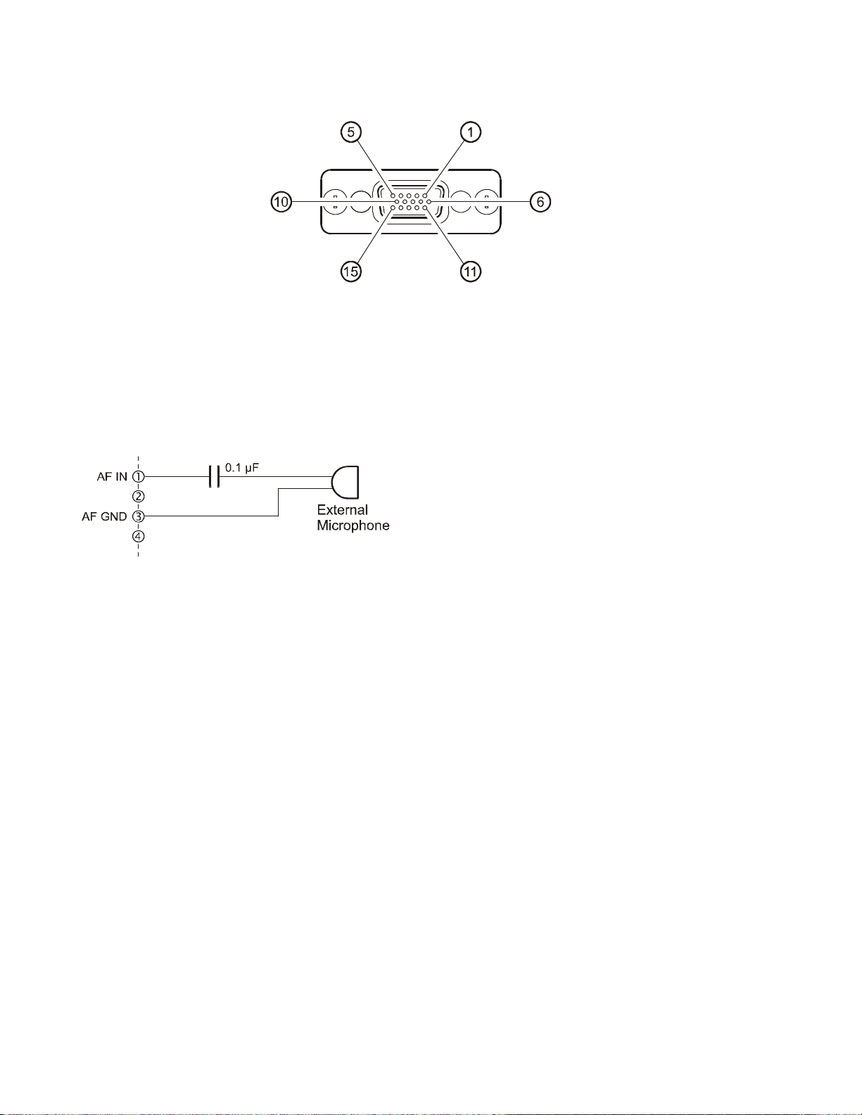
DSUB 15-pin Accessory Connector
Pin 1: AF IN (ANALOG INPUT
External Microphone Input. Nominal input level is 6
mV at 600-ohm.
When connect the External Microphone to this port,
insert a 0.1 μF coupling capacitor between the microphone and this port; as shown illustlation.
Pin 2: AF OUT (ANALOG OUTPUT
Low-level receiver output. Peak signal level is 150 mV
at 600-ohm.
)
)
Pin 3: AF GND
Ground for all logic levels and power supply return.
Pin 4: DC OUT (13.6 V DC OUTPUT
Switched 13.6V output for supplying power to an accessory.
Pin 5: RSSI (ANALOG OUTPUT
A DC voltage proportional to the strength of the signal currently being received (Receiver Signal Strength
Indicator) is provided on this pin. This low impedance
output is gererated by the receiver IF sub-system and
bufferd by an internal op-amp. Typical output voltages are 1 V (@No Signal Input) through 2.0 V (@50 dB
Signal Input).
)
)
Pin 6: EXT PTT
Shorting this port to ground causes the transceiver to
be placed in the Transmit mode, while opening the
connection to this port returns the transceiver to the
Receive mode. Opening voltage is 5 V, closed current
approx. 5 mA.
Pin 7: TRX
This port is intended for controlling an external TX/
RX switching circuit. This port is open collector output which can sink approx. 100 mA when active. Max.
voltage is 16V.
Pin 8: IGN (IGNITION SENSE FEATURE
The VX-2100/-2200 may be automatically be switched
to the STND-BY mode when the vehicle's ignition key
is turned on. Maximum current is 20 mA.
)
Pin 9 - 12: ACC1 - ACC4 (ACCESSORY PORT)
These port features can be programmed via the CE82
programmer. Each port is open collector output which
can sink approx. 100 mA when active. Max. output 16V.
When the input is selected, it becomes active between
2V and 16V.
Pin 13: ACC5 (ACCESSORY PORT)
The port 5 is available to set only for Output function,
and active logic is the opposite side against the Port 1
~ 4.
Max.output 5V, closed current approx. 1 mA.
(CMOS output)
Pin 14: ACC6 (ACCESSORY PORT)
The port 6 is available to set only for Input function,
and active logic is the opposite side against the Port 1
~ 4.
Max.input 5V. (CMOS input)
Pin 15: GND
Chassis ground
VX-2100/-2200 (UHF
)
Service ManaulB-1
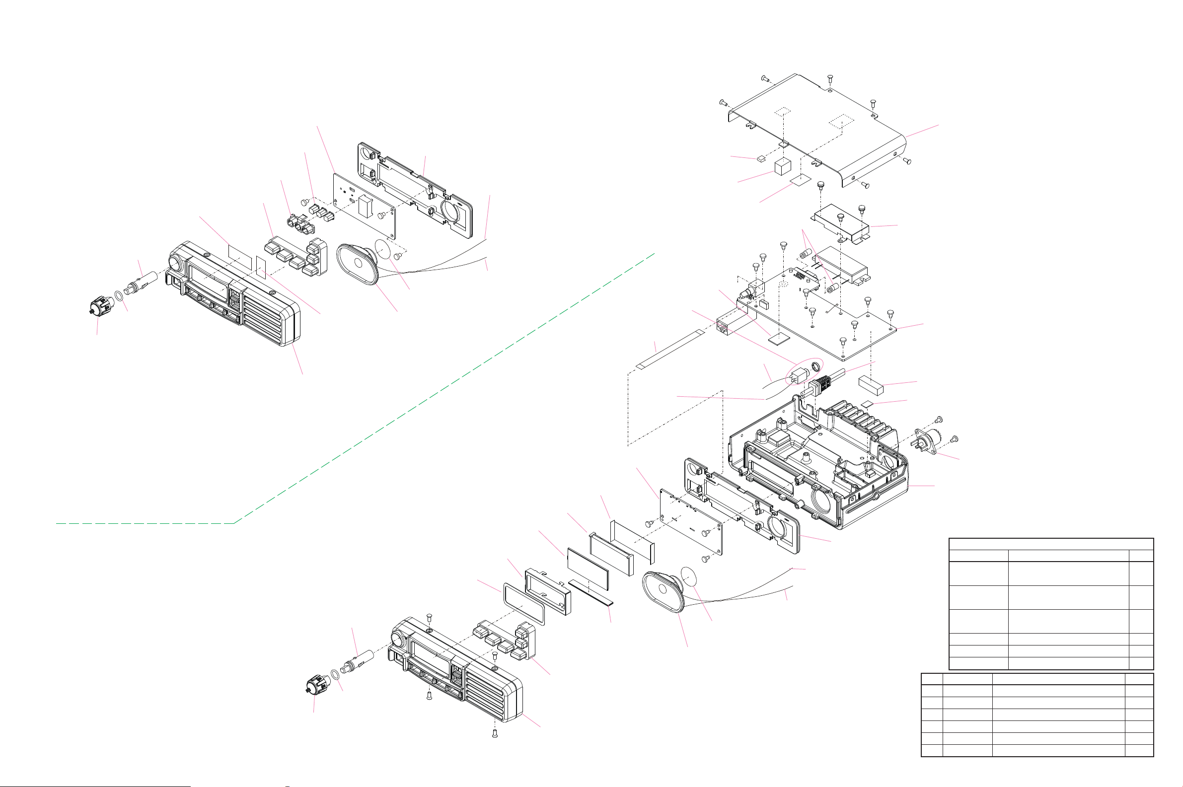
Exploded View & Miscellaneous Parts
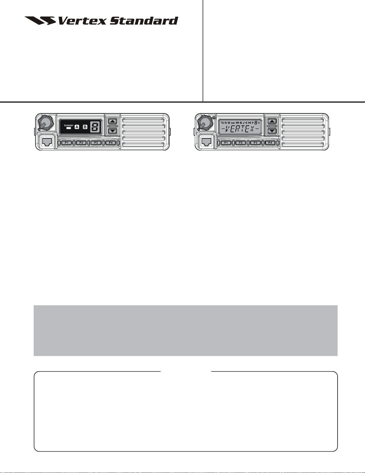
VX-2100 FRONT PANEL
RA1062100
MYLAR SHEET
RA0788600
JOINT
RA0746700
O RING
RA0788500
VOLUME KNOB
RA0787600
LIGHT GUIDE (x3 pcs)
RA078750A
HOLDER
RA0845300
RUBBER KNOB
FRONT-A-UNIT
RA0997300
LED FILTER
RA079170A
FRONT PANEL ASSY
(w/ WINDOW (8ch))
RA080360A
RUBBER PACKING
RA0821900
SPONGE RUBBER
M4090179A
SPEAKER
T9318283
WIRE ASSY (RED)
T9318284
WIRE ASSY (BLK)
P1090654
CONNECTOR
T9207042
WIRE ASSY
T9318286
WIRE ASSY
(WHT)
RA0841400
BLIND SHEET
RA0800600
SPONGE RUBBER
RA0871100
ELEC. COND T APE 2520
This nut are attached to
DSUB CONNECTOR.
RA0790700
PAD (AMP)
T9318285
WIRE ASSY (GRN)
RA0790200
TOP CASE
RA0790300
SHIELD CASE
MAIN-UNIT
T9207044A
WIRE ASSY
RA0848100
PAD (LPF)
RA0790800
PAD (DIODE)
VX-2200 FRONT PANEL
VX-2100/-2200 (UHF) Service Manaul
RA0788600
JOINT
RA0746700
O RING
RA0788500
VOLUME KNOB
RA0786300
LCD HOLDER
RA0786900
SPONGE RUBBER
G6090173
LCD
FRONT-B-UNIT
RA0790900
REFLECTOR SHEET
RA078640A
LIGHT GUIDE
RA0786200
INTER CONNECTOR
RA0845300
RUBBER KNOB
RA079160A
FRONT PANEL ASSY
(w/ LIGHT GUIDE, WINDOW)
RA0821900
SPONGE RUBBER
M4090179A
SPEAKER
RA080360A
RUBBER PACKING
T9318284
WIRE ASSY (BLK)
T9318283
WIRE ASSY (RED)
P1091172
CONNECTOR
RA079000D
CHASSIS
Non-designated parts are available only as
part of a designated assembly.
SUPPLIED ACCESSORIES
VXSTD P/N DESCRIPTION QTY.
Q0000075 BLADE FUSE 15A (45 W)
Q0000112 BLADE FUSE ATC 10A (25 W)
AAE60X001
T9021010 DC CABLE (25 W)
T90210151 DC CABLE (45 W)
RA079050A MOBILE BRACKET 1
RA0790600 KNOB SCREW (for BRACKET) 2
U9900209 HEX HEAD BOLT HSM5X12B 2
No. VXSTD P/N DESCRIPTION QTY .
U10206007 TRUSS HEAD SCREW M2.6X6B 10
U24308002 TAPTITE SCREW M3X8NI 13
U03308002 SEMS SCREW ASM3X8NI 2
U24306002 TAPTITE SCREW M3X6NI 2
U71002001 SPRING LOCK WASHER SW2.6 2
U76003001 PLAIN WASHER AW3 2
MICROPHONE MH-67A8J
W/ CLIP
2
1
1
C-1

Exploded View & Miscellaneous Parts
Note:
C-2
VX-2100/-2200 (UHF) Service Manaul
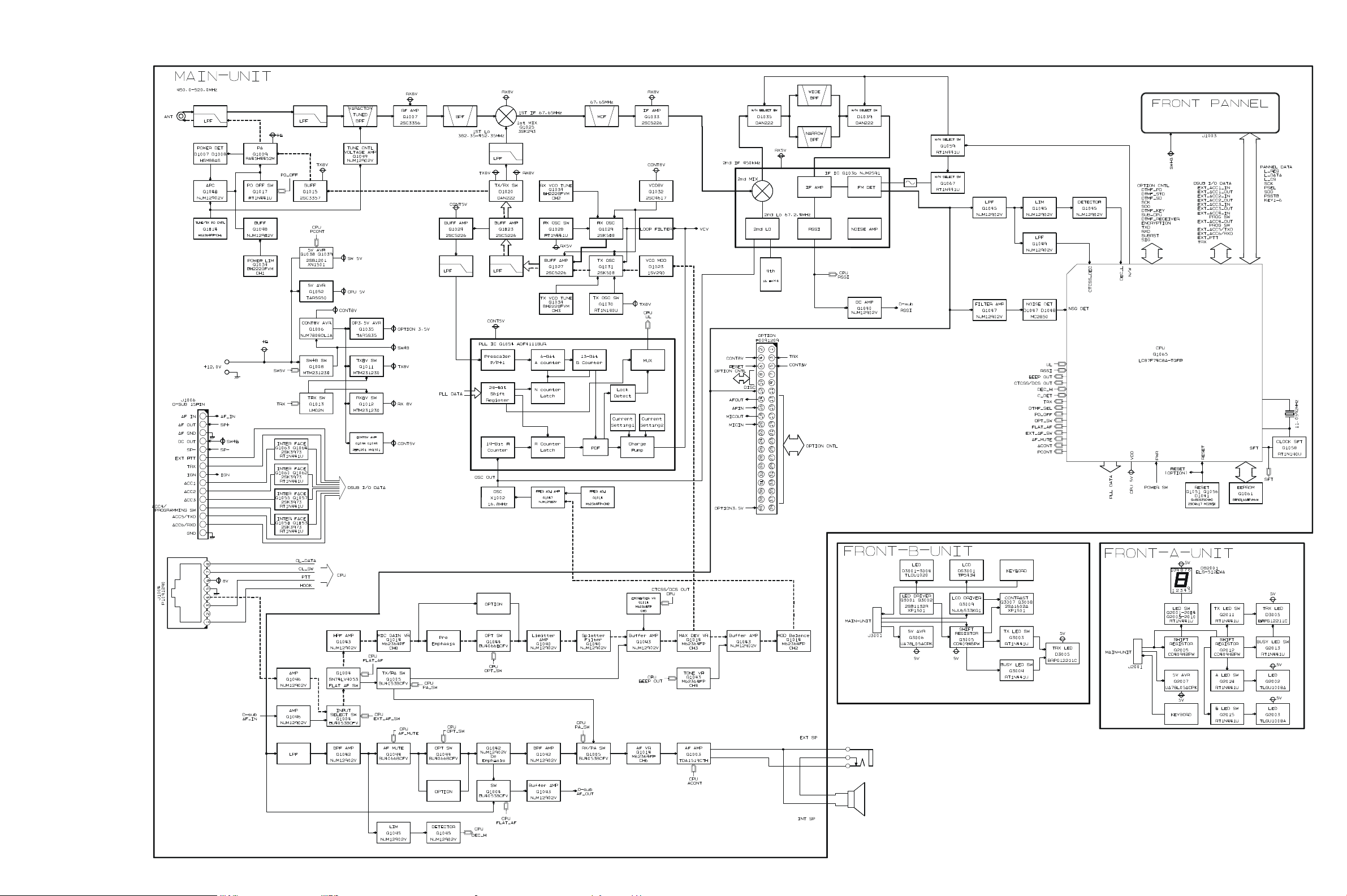
Block Diagram
VX-2100/-2200 (UHF) Service Manaul
D-1

Block Diagram
Note:
D-2
VX-2100/-2200 (UHF) Service Manaul

Circuit Description
1. Circuit Configuration by Frequency
The receiver is a double-conversion superheterodyne with
a first intermediate frequency (IF) of 67.65 MHz and a
second IF of 450kHz. The incoming signal from the antenna is mixed with the local signal from the VCO/PLL to
produce the first IF of 67.65MHz. This is then mixed with
the 67.2 MHz second local oscillator output to produce
the 450 kHz second IF. This is detected to give the demodulated signal.The transmit signal frequencyis generated by the PLL VCO and modulated by the signal from
the microphone. It is then amplified and sent to the antenna.
2. Receiver System
2-1. Front-end RF amplifier
The incoming RF signal from the antenna is delivered to
the RF Unit and passes through the Low-pass filter which
removes undesired frequencies by use of varactor diodes,
tuned band-pass filter consisting of diodes D1004 and
D1005 (both 1SV323), and Coils L1006 and L1009, capaci-
tors C1013, C1016, C1033, C1041 and C1044.
The passed signal is amplified in Q1007 (2SC3356) and
moreover cuts an image frequency with the band pass
filter consisting of Coils L1011, L1013, L1014, and L1015,
capacitors C1103 C1111, C1112, C1116, C1122, C1123,
C1127, C1128, C1130, C1039, C1134, and C1141, and comes
into the 1st mixer.
2-2. First Mixer
The 1st mixer consists of the Q1025 (3SK293). Buffered
output from the VCO is amplified by Q1024 (2SC5226)
to provide a purefirst local signal (receiving fequency plus
67.65 MHz) for injection to the first mixer. The output IF
signal is entersfrom the mixer to the crystal filter. The IF
signal then passesthrough monolithic crystal filters
XF1001 (±5.5 kHz BW) to strip away all but the desired
signal.
2-3. IF Amplifier
The first IF signal is amplified by Q1033 (2SC5226). The
amplifiedfirst IF signal is applied to FM IF subsystem IC
Q1036 (NJM2591V) which contains the second mixer sec-
ond local oscillator limiter amplifier noise amplifier and
S-meter amplifier. The signal from the refernce oscillator
is tripled by Q1033 (2SC5226), it is mixed with the IF
signal and becomes 450 kHz. The second IF then passes
through the ceramic filter CF1001 (for wide channels)
CF1002 (for narrow channels) to strip away unwanted
mixer products which removes amplitude variations in
the 450 kHz IF before detection of the speech by the
ceramicdiscriminator CD1001.
2-4. Audio amplifier
Detected signal from Q1036 (NJM2591V) is inputted to
Q1042 (NJM12902V) and is output through the band pass
filter inside Q1042 (NJM12902V). When the optional unit
is installed Q1044 (BU4066BCFV) is turned “OFF” and
the AF signal from Q1042 (NJM12902V) goes the optional
unit. When the optional unit is not installed, Q1042
(NJM12902V) is turned "ON" and the signal goes through
Q1004 (BU4053BCFV). The signal then goes through AF
mute switch Q1044 (BU4066BCFV) de-emphasis part
Q1042 (NJM12902V). amplified with AF power ampli-
fier Q1003 (TDA1519CTH) after passing AF volume
Q1014 (M62364FP). The output of Q1003 (TDA1519CTH)
drives a speaker (either the internal or external speaker).
2-5. Squelch Circuit
There are 13 levels of squelch setting from 0 to 12. The
level 0 means open the squelch. The level 1 means the
threshold setting level and level 11 means tight squelch.
From 2 to 10 is established in the middle of threshold and
tight. The bigger figure is nearer the tight setting. The level
12 becomes setting of carrier squelch.
2-5-1. Noise Squelch
The noise squelch circuit is composed of the band pass
filter of Q1036 (NJM2591V) noise amplifier Q1047
(NJM12902V) and noise detector D1047, D1048 (both
MC2850). When a carrier isn't received, the noise ingre-
dient which goes out of the demodulator Q1036
(NJM2591V) is amplified in Q1047 (NJM12902V) through
the band pass filter Q1036 (NJM2951V) is detected to DC
voltage with D1047 and D1048 (both MC2850), and is in-
putted to 15 pin (the A/D port) of the Q1065 (CPU:
LC87F5CC8A). When a carrier is received the DC volt-
age becomes “LOW” because the noise is compressed.
When the detected voltage to CPU is “HIGH,” the CPU
stops AF output with Q1044 (BU4066BCFV) “OFF” by
making pin 80 low. When the detection voltage is low the
CPU makes Q1044 “ON” making pin 80 “H” enabling
AF output.
2-5-2. Carrier Squelch
The Pin 14 (A/D port) of Q1065 (CPU: LC87F5CC8A) de-
tects RSSI voltage output from pin 12 of Q1036
(NJM2591V), and controls AF output. The RSSI output
voltage changes according to the signal strength of carrier. The stronger signal makes the RSSI voltage higher.
The process of the AF signal control is the same as Noise
Squelch. The shipping data is adjusted 3dB higher than
squelch tight sensitivity.
VX-2100/-2200 (UHF) Service Manaul
E-1

Circuit Description
3. Transmitter System
3-1. Mic Amplifier
There are two micrphone inputs, J1004 (front) and J1006
(D-Sub). Each microphone inputs has it's own amplifier.
Which micrphone is selected is controlled by the CPU and
in addition, the amplified AF signal is selected with Flat-
AF selection switch Q1043 (NJM12902V). Mic Gain is
adjusted with Mic gain VR Q1014 (M62364PF) through
HPF-AMP Q1043 (NJM12902V), and Pre Enphasis and
Mic Mute Q1044 (BU4066BCFV) are passed at FLAT-AF
OFF. And, the option use is selected with OPT selection
switch Q1044 (BU4066BCFV) by the control from CPU.
The selected signal enters maximum deviation adjustment
volume Q1014 (M62364FP) after it goes out of Buffer Amp
Q1043 (NJM12902V) through limiter and splatter filter
of Q1040 (NJM12902V). The adjusted low frequency signal ingredient is amplified by Q1045 (NJM12902V) added
modulation terminal of TCXO (X1002) the FM modulation is made by reference oscillator. The high frequency
signal ingredient is amplified Q1043 (NJM12902V), and
the level is adjusted by volume control Q1014 (M62364FP)
to make frequency balance between low frequency. After
that, the signal is delievered to the tranmsit carrier by
modulator D1023 (HVC300A).
3-4-1. VCO
While the radio is receiving, the RX oscillator Q1029
(2SK508) in the VCO generates a programmed frequency
(receive frequncy plus 67.65 MHz) as 1st local signal.
While the radio is transmitting the TX oscillator Q1031
(2SK508) in the VCO generates a frequency (transmit
frequncy). The output from oscillator is amplified by
buffer amplifier Q1027 (2SC5226) and becomes the out-
put of the VCO. The output from VCO is divided one is
amplified by Q1024 (2SC5226) and feed back to pin 6 of
the PLL IC Q1054 (ADF4111BRU). The other is amplified
in Q1023 (2SC5226) and in case of the reception it is put
into the mixer as the 1st local signal through D1020
(DAN222) in transmission it is amplified in Q1027
(2SC5226) and more amplified in Q1023 (2SC5226)
through D1022 (DAN222) and it is put the input terminal
of the Power Module Q1009.
3-4-2. VCV CNTL
Tuning voltage (VCV) of the VCO expands the lock range
of VCO by controlling the of varactor diode voltage and
the control voltage from PLL IC Q1054 (ADF4111BRU).
Control voltage is added to the varactor diode after con-
verted to D/A converter Q1014 (M62364FP).
3-2. Drive and Final amplifier
The modulated signal from the VCO Q1031 (2SK508) is
buffered by Q1027 (2SC5226) and amplified by Q1015
(2SC3357). The low-level transmit signal is then applied
to the Power Module Q1009 (RA55H4047M for version A
or RA45H4452M for version D) for final amplification up
to 45 watts output power or (S-AU83AL for version A, S-
AU83AH for version D, or RA30H3340M for version I)
for final amplification up to 25 watts output power. The
transmit signal then passes through a low-pass filter to
suppress harmonic spurious radiation before delivery to
the antenna.
3-3. Automatic Transmit Power Control
The output power of Power Module is detected by CM
coupler, and is detected by D1007 and D1008 (both
HSM88AS) and is inputted to comparator Q1048
(NJM12902V). The comparetor compares two different
voltages and makes output power stable by controlling
the bias voltage of the power module. There are 3 levels
of output power (Hi, Mid and Lo) which is switched by
the voltage of Q1014-CH1 (M62364FP).
3-4. PLL Frequency Synthesizer
The frequency synthesizer consists of PLL IC Q1054
(ADF4111BRU) VCO, TCXO (X1002) and buffer ampli-
fier. The output frequency from TCXO is 16.8 MHz and
the tolerance is ±2.5 ppm (in the temperature range -30 to
+60 degrees).
E-2
3-4-3. PLL
The PLL IC Q1054 (ADF4111BRU) consists of reference
divider, main divider, phase detector, charge pumps and
Pulse Swallow Frequency Synthesis. The reference frequency from TCXO is inputted to pin 8 of PLL IC Q1054
(ADF4111BRU) and is divided by reference divider. This
IC is decimal point dividing PLL IC Q1054 (ADF4111BRU)
and the dividing ratio becomes 1/8 of usual PLL frequency
step. Therefore, the output of reference divider is 8 times
of frequencies of the channel step. For example when the
channel stepping is 5 kHz, the output of reference divider
becomes 40 kHz. On the other hand, inputted feed back
signal to pin 6 of PLL IC Q1054 (ADF4111BRU) from VCO
is divided with the dividing ratio which becomes same
frequency as the output of reference divider. These two
signals are compared by phase detector, a phase pulse is
generated. The phase difference pulse and the pulse from
fractional accumulator pass through the charge pumps
and LPF. This becomes the DC voltage (VCV) to control
the VCO. The oscillation frequency of VCO is locked by
the control of this DC voltage. The PLL serial data from
CPU Q1065 (CPU: LC87F5CC8A) is sent with three lines
of SDO (pin 12), SCK (pin 11) and PSTB (pin 13). The lock
condition of PLL is output from the UL (pin 14) terminal
and UL becomes “H” at the time of the lock condition
and becomes “L” at the time of the unlocked condition.
The CPU Q1065 (CPU: LC87F5CC8A) always watches
over the UL condition, and when it becomes “L” unlocked
condition, the CPU Q1065 (CPU: LC87F5CC8A) prohib-
its transmitting and receiving.
VX-2100/-2200 (UHF) Service Manaul

Alignment
Introduction
The VX-2100/-2200 series has been aligned at the factory
for the specified performance across the entire frequency
range specified. Realignment should therefore not be necessary except in the event of a component failure. All component replacement and service should be performed only
by an authorized Vertex Standard representative, or the
warranty policy may be voided.
The following procedures cover the sometimes critical and
tedious adjustments that are not normally required once
the transceiver has left the factory. However, if damage
occurs and some parts are replaced, realignment may be
required. If a sudden problem occurs during normal operation, it is likely due to component failure; realignment
should not be done until after the faulty component has
been replaced.
We recommend that servicing be performed only by authorized Vertex Standard service technicians who are experienced with the circuitry and fully equipped for repair and alignment. Therefore, if a fault is suspected, contact the dealer from whom the transceiver was purchased
for instructions regarding repair. Authorized Vertex Standard service technicians realign all circuits and make complete performance checks to ensure compliance with factory specifications after replacing any faulty components.
Those who do undertake any of the following alignments
are cautioned to proceed at their own risk. Problems
caused by unauthorized attempts at realignment are not
covered by the warranty policy. Also, Vertex Standard
must reserve the right to change circuits and alignment
procedures in the interest of improved performance, without notifying owners. Under no circumstances should any
alignment be attempted unless the normal function and
operation of the transceiver are clearly understood, the
cause of the malfunction has been clearly pinpointed and
any faulty components replaced, and the need for realignment determined to be absolutely necessary. The following test equipment (and thorough familiarity with its correct use) is necessary for complete realignment. Correction of problems caused by misalignment resulting from
use of improper test equipment is not covered under the
warranty policy. While most steps do not require all of
the equipment listed, the interactions of some adjustments
may require that more complex adjustments be performed
afterwards. Do not attempt to perform only a single step
unless it is clearly isolated electrically from all other steps.
Have all test equipment ready before beginning, and follow all of the steps in a section in the order presented.
Required Test Equipment
Radio Tester with calibrated output level at 1 GHz
In-line Wattmeter with 5% accuracy at 1 GHz
50-ohm, 100-W RF Dummy Load
Regulated DC Power Supply (standard 13.6V DC, 15A)
Frequency Counter: ±0.2 ppm accuracy at 1 GHz
AF Signal Generator
AC Voltmeter
DC Voltmeter
UHF Sampling Coupler
Microsoft® Windows® 95 or later operating system
Vertex Standard VPL-1 Connection Cable and CE82
Alignment program
Alignment Preparation & Precautions
A 50-ohm RF Dummy load and in-line wattmeter must
be connected to the main antenna jack in all procedures
that call for transmission, except where specified otherwise. Correct alignment is not possible with an antenna.
Beacuse of the BTL (Bridged TransLess) Amplifier circuit
used in the VX-2200/-2100, do not connect eather side of
the speaker leads to chassis “ground.”
After completing one step, read the following step to determine whether the same test equipment will be required.
If not, remove the test equipment (except dummy load
and wattmeter, if connected) before proceeding.
Correct alignment requires that the ambient temperature
be the same as that of the transceiver and test equipment,
and that this temperature be held constant between 68 °F
and 86 °F (20 °C ~ 30 °C). When the transceiver is brought
into the shop from hot or cold air, it should be allowed
time to come to room temperature before alignment.
Whenever possible, alignments should be made with oscillator shields and circuit boards firmly affixed in place.
Also, the test equipment must be thoroughly warmed up
before beginning.
Note: Signal levels in dB referred to in this procedure are
based on 0 dBμ EMF = 1.0 μV.
VX-2100/-2200 (UHF) Service Manaul
F-1
Alignment
Test Setup
Setup the test equipment as shown for transceiver alignment, apply 13.6V DC power to the transceiver. Refer to
the drawings above for Alignment Points.
50-ohm
Dummy Load
Inline
Wattmeter
Deviation Meter
Frequency
Counter
RF Sampling
Coupler
ANT
VPL-1
Connection Cable
COM Port
RF
Signal Generator
Transceiver
MIC
DC INPUT
Power Supply
13.6 VDC
The Alignment T ool Outline
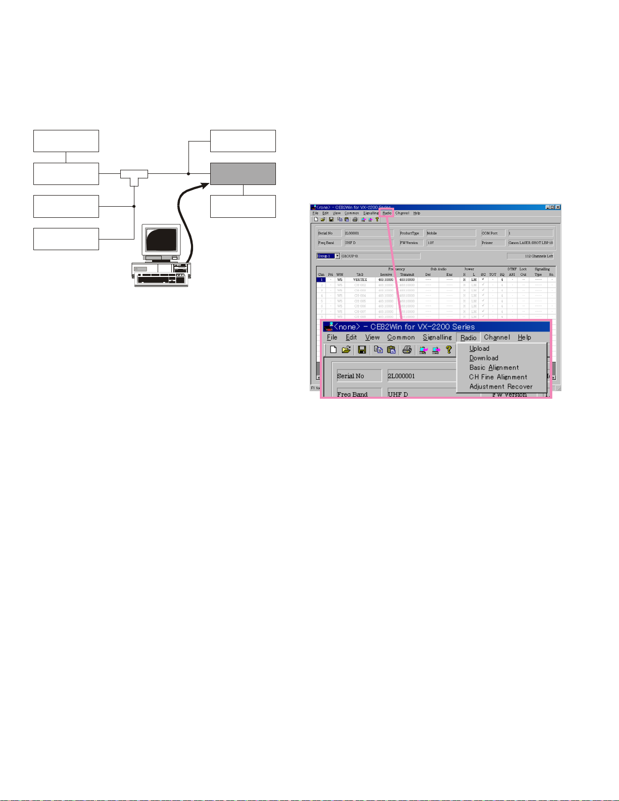
Installation the tool
Install the CE82 (Clone Editor) to your PC.
The re-alignment for VX-2200/-2100 series may use the
“Alignment” menu of CE82.
Basic Alignment Mode
The Basic Alignment mode allows you to align the entire
radio. The value of each parameter can be changed to the
desired position by use of the “” / “” and up/down
arrow keys, along with direct number input and dragging of the PC mouse.
To enter the Basic Alignment Mode, select “Basic Alignment” in the main “Radio” menu. It will start to “Upload”
the written personalized data from the radio. Pressing the
“OK” button will then start the Basic Alignment Mode.
Action of the switches
When the transceiver is in alignment mode, the action of
PTT and KEY is ignored. All of the action is remote controlled by PC.
Note: when all items are to be aligned, it is strongly recommended to align them according to following sequence.
When the item is selected with TAB key, and the F1 key is
pushed, the “Help” file is displayed.
Detailed information for each step may be found in the
“Help” file within CE82 (Clone Editor).
1. RX VCO Tune Voltage (RX VCO)
2. TX VCO Tune Voltage (TX VCO)
3. PLL Reference Frequency (Frequency)
4. RX Sensitivity (RX Tune)
5. Squelch (SQL)
6. TX Power
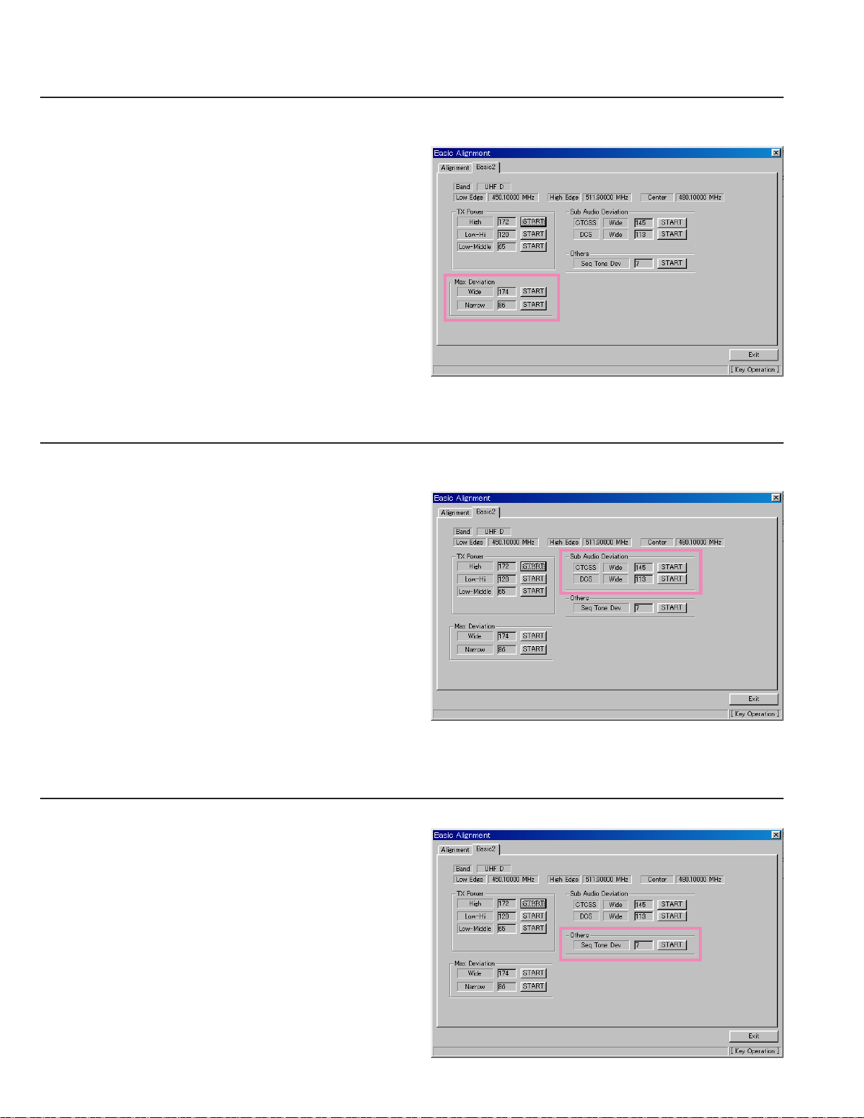
7. Maximum Deviation <Wide> / <Narrow>
8. Sub Audio Deviation <CTCSS> / <DCS>
9. Sequential Tone Deviation
F-2
VX-2100/-2200 (UHF) Service Manaul
Alignment
Unit
During alignment, the values of dBμV or μV (EMF
or PD) can be selected or dBm.
1. RX VCO Tune Voltage (RX VCO)
This parameter is to align the “Tune Voltage” of RX VCO. This alignment will be done automatically between the radio
and PC.
1. Press the “Start” button on the "Basic Alignment" window to open the RX VCO Adjustment window.
2. Press the “Start” button to start the alignment then the
“OK” and “Cancel" buttons are inhibited during the
alignment.
3. The aligned value will appear and the “OK”, “Cancel” buttons come alive when auto-alignment is finished.
4. Press the “OK” button on the window, the value of the
alignment for RX VCO will be saved in the radio.
2. TX VCO Tune Voltage (TX VCO)
This parameter is to align the “Tune Voltage” of TX VCO. This alignment will be done automatically between the radio
and PC.
1. Press the “Start” button on the “Basic Alignment” window to open the TX VCO Adjustment window.
2. Press the “Start” button to start the alignment then the
“OK” and "Cancel" buttons are inhibited during the
alignment.
3. The aligned value will appear and the “OK”, “Cancel” buttons come alive when auto-alignment is finished.
4. Press the “OK” button on the window, the value of the
alignment for TX VCO will be saved in the radio.
VX-2100/-2200 (UHF) Service Manaul
F-3
Alignment
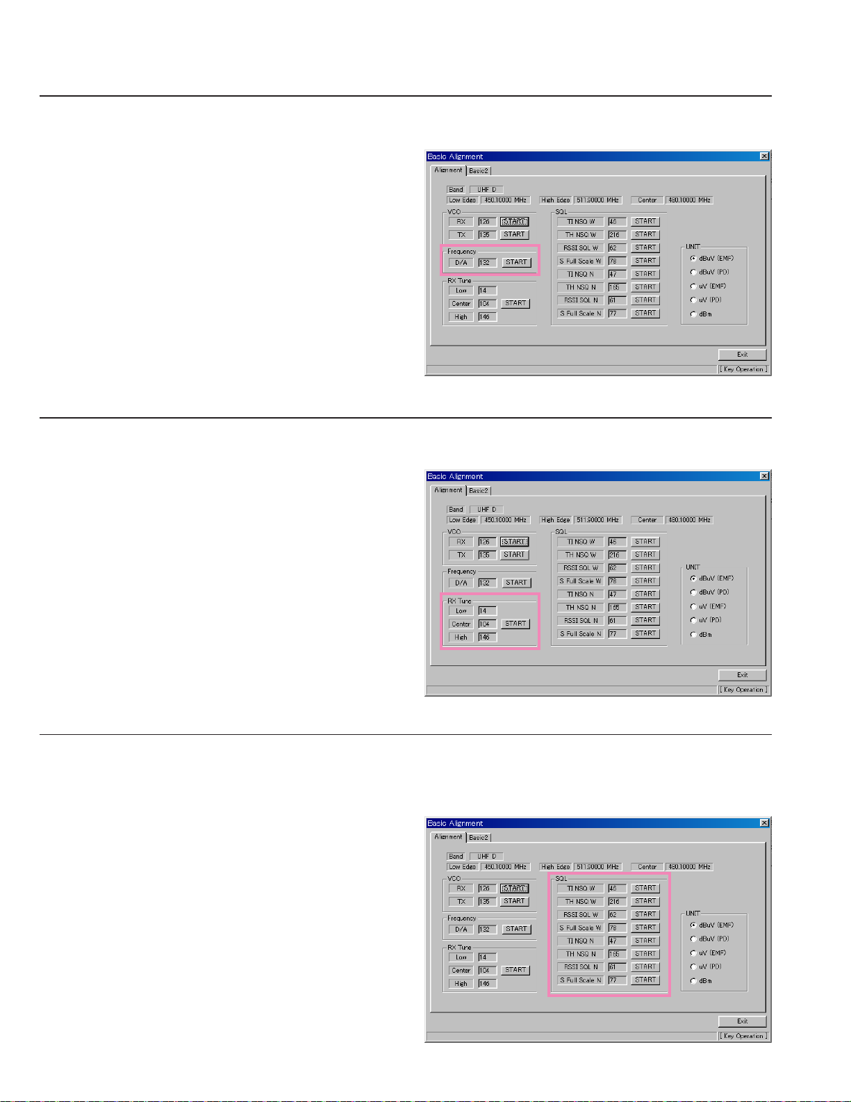
3. PLL Reference Frequency (Frequency)
This parameter is to align the reference frequency for PLL. The “TX VCO Tune Voltage” alignment must be done before
this alignment is going to start.
1. Press the “Start” button to start the alignment then the
radio will transmit on the center frequency. It will appear the Frequency Alignment window.
2. Set the value to get desired frequency by left/right arrow key, drag the slide bar by mouse or direct number
input.
3. Press the “OK” button on the alignment window to
save the re-aligned value, the alignment of the PLL Reference Frequency is accomplished.
4. RX Sensitivity (RX Tune)
This parameter is to align the RX BPF (Band Pass Filter) for Rx sensitivity. It must be done both alignments of the “RX
VCO Tune Voltage” and “PLL Reference Frequency” before this alignment is going to start.
1. Press the “Start” button to start the alignment.
2. Set the Signal Generator according to the indication,
then press “OK”.
3. Repeat the procedure no.2 until the 3point alignment
is finished.
4. It will show the result of 3 points alignment and press
“OK” then the confirmation window will open.
5. Press “OK” to finish the RX Sensitivity alignment and
save the data.
5. Squelch (SQL)
This parameter is to align the SQL (Squelch) Sensitivity. The “RX VCO Tune Voltage”, “PLL Reference Frequency” and
“RX Sensitivity (RX Tune)” must be done before this alignment is started.
There are several alignments as follows in the Squelch Sensitivity.
Noise SQL Tight <Wide> (TI NSQ W)
The Alignment for the Noise SQL Tight level at Wide (5k/
4k).
Noise SQL Threshold <Wide> (TH NSQ W)
The Alignment for the Noise SQL Threshold level at Wide
(5k/4k).
RSSI SQL Level 11 <Wide> (RSSI SQL W)
The Alignment for the “level 11” of the RSSI SQL level at
Wide (5k/4k).
F-4
VX-2100/-2200 (UHF) Service Manaul
RSSI SQL Full Scale <Wide> (S Full Scale W)
The Alignment for the RSSI Full Scale level at Wide (5k/
4k).
Noise SQL Tight <Narrow> (TI NSQ N)
The Alignment for the Noise SQL Tight level at Narrow
(2.5k).
Noise SQL Threshold < Narrow > (TH NSQ N)
The Alignment for the Noise SQL Threshold level at Narrow (2.5k).
RSSI SQL Level 11 < Narrow > (RSSI SQL N)
The Alignment for the “level 11” of the RSSI SQL level at
Narrow (2.5k).
RSSI SQL Full Scale < Narrow > (S Full Scale N)
The Alignment for the RSSI Full Scale levle at Narrow
(2.5k).
The procedure for all the alignment is as follows.
1. Press the “Start” button to start the alignment.
2. Set the signal generator according to the level indicated, then press “OK”.
3. Press the “OK” button after finish the alignment, then
the data will be saved and the alignment is accomplished.
Alignment
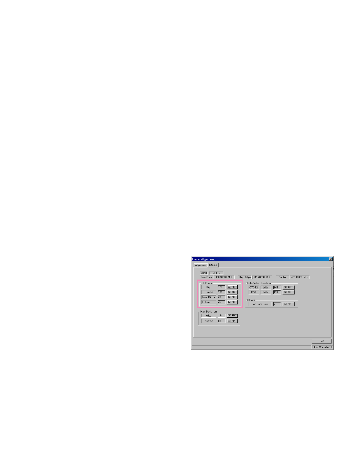
6. TX Power
Open the “Basic2” window, this parameter is to align the Transmit Output (Hi/Low) Power.
The factory default is as followings.
45 W nodel 25 W model
High 45 W 25 W
Low-High 25 W 12.5 W
Low-Middle 10 W 5 W
E-Low –– 1 W
The procedure for the alignments of the TX Power is followings.
1. Press the “Start” button to start the alignment then the
radio will transmit on the center frequency. The TX
Power Alignment window will open on the PC.
2. Set the value to get desired output power by left/right
arrow key, drag the slide bar by mouse or direct number input.
3. Press the “OK” button on the alignment window to
save the re-aligned value, the alignment of the TX
POWER is accomplished.
VX-2100/-2200 (UHF) Service Manaul
F-5
Alignment
7. Maximum Deviation <Wide> / <Narrow>
This parameter is to align the Maximum Deviation (Wide/Narrow). The “TX VCO Tune Voltage” must be done before
this alignment is started.
1. Press the “Start” button to start the alignment.
2. Set the value to get desired deviation (Wide: 4.2kHz,
Narrow: 2.1kHz) on the deviation meter by changing
the slide bar on your PC.
3. Press the “OK” button after getting the desired Deviation to save the re-aligned value, the alignment of the
MAX DEVIATION is accomplished.
8. Sub Audio Deviation <CTCSS> / <DCS>
This parameter is to align the Deviation of Sub-Audio (CTCSS/DCS). The “TX VCO Tune Voltage” and “Max Deviation”
must be done before this alignment is started.
1. Press the “Start” button to start the alignment.
2. Set the value to get desired deviation (Wide: 0.6kHz)
on the deviation meter by changing the slide bar on
your PC.
3. Press the “OK” button after getting the desired value
to save the re-aligned value, the alignment of the MAX
DEVIATION is accomplished.
9. Sequential Tone Deviation
This parameter is to align the “Sequential Tone Deviation” (for 2-Tone, 5-Tone and DTMF sequential tones).
1. Press the “Start” button to start the alignment.
2. Set the value to get desired deviation by changing the
slide bar on your PC.
3. Press the “OK” button after getting the desired value
to save the re-aligned value, the alignment of the SEQUENTIAL TONE DEVIATION is accomplished.
F-6
VX-2100/-2200 (UHF) Service Manaul
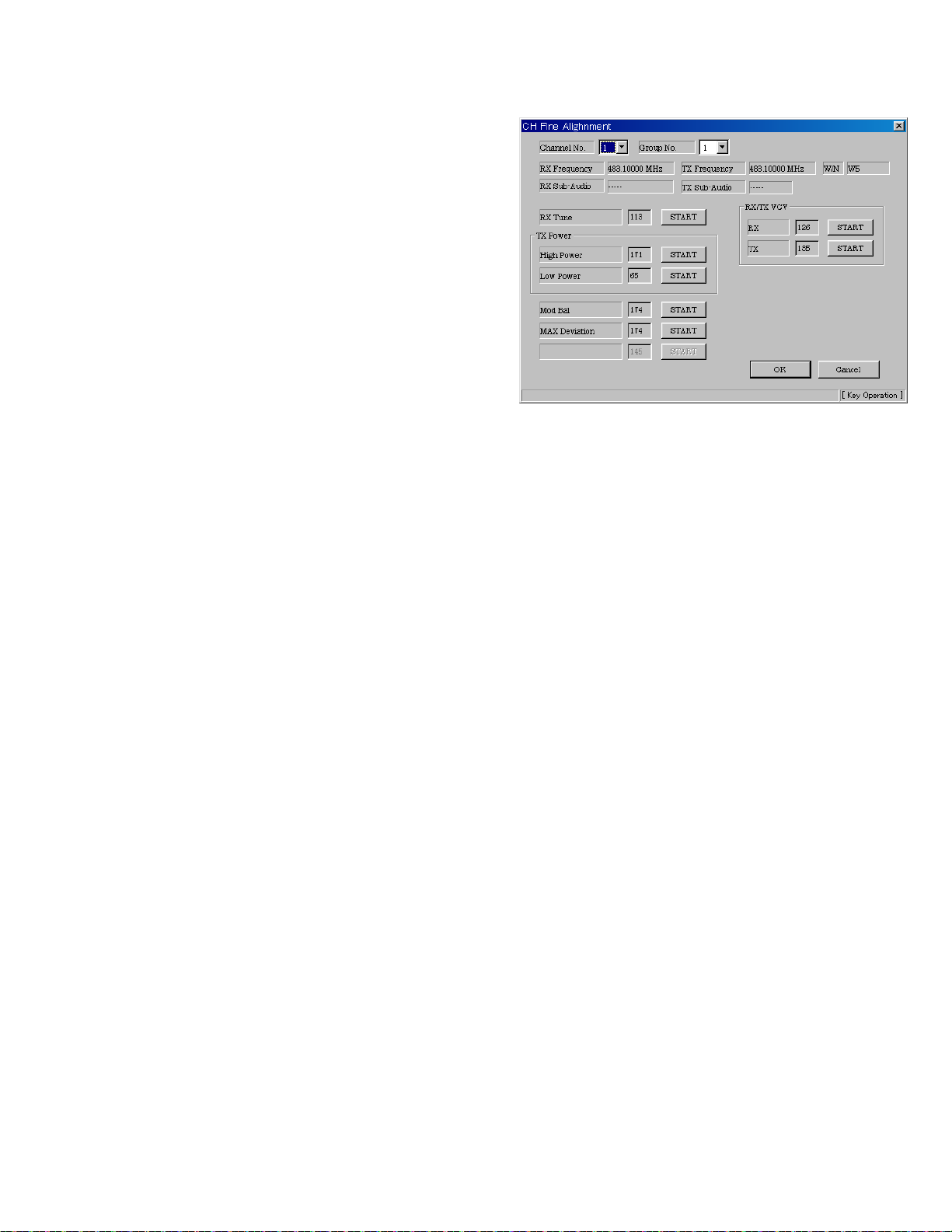
CH (Channel-by-Channel) Fine Alignment Mode
The CH Fine Alignment Mode allows you to align the radio separately for every operating channel. The value of
each parameter can be changed to the desired position using the “” / “” and up/down arrow keys, direct number
input, and by dragging the PC mouse.
To enter the CH Fine Alignment Mode, select “CH Fine
Alignment” in the main “Radio” menu. It will start to “Upload” the written personalized data from the radio. Pressing the “OK” button will then start the CH Fine Alignment
Mode.
Note: Detailed information for each step may be found in
the “Help” file within CE82 (Clone Editor).
Alignment
VX-2100/-2200 (UHF) Service Manaul
F-7
Installation of Option
FVP-25/FVP-35/FVP-36
The FVP-25 is an Encryption/DTMF Pageing Unit which
permits secure voice communications with station within
your network, while preventing others from listening using normal communications equipment. It allows paging,
and enables selective calling using DTMF tone sequences.
The FVP-35 is an Rolling Code Encryption Unit which
permits secure voice communications with station within your network, while preventing others from listening
using normal communications equipment.
The FVP-36 is an Voice Inversion Type Encryption Unit
which permits secure voice communications with station
within your network, while preventing others from listening using normal communications equipment.
Each optional Unit is easily programmed the configulationsp using a Vertex CE82 programmer with an IBM PCcompatible computer.
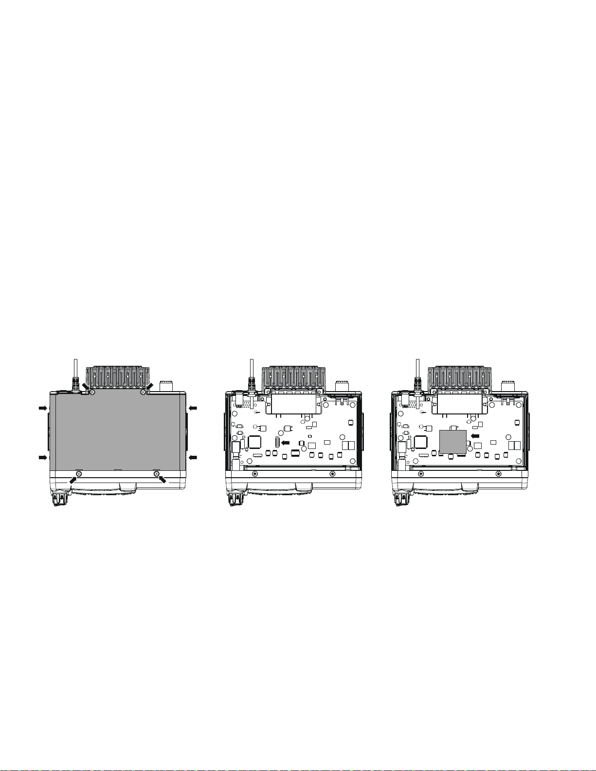
1. Disconnect the DC power cable.
2. Referring to Figure 1, remove the 8 screws affixing the
Top Cover, then remove the top cover.
3. Referring to Figure 2 & Figure 3, locate the empty connector for the Optional Unit, connect the Optional Unit
here.
4. Replace the Top Cover and 8 screws. Installation is now
complete.
Do not install all Optional Unit at onece.
Figure 1
Figure 2
Figure 3
G-1
VX-2100/-2200 (UHF) Service Manaul
-120 dBm
RX:1.9V -86.0 dBm
TX:0V -88.5 dBm (C1046 removed)
RX:7.6V
TX:0V
RX:0V
TX:1.5V
POWER OFF:0.4V
POWER ON:13.6V
RX:2.6V
TX:1.8V
RX:0V
TX:8.1V
RX:1.1V
TX:0V
RX:13.6V
TX:13.6V
8.1V
RX:7.6V
TX:0V
-100.5 dBm
-106.0 dBm (C1093 removed)
+12.3dBm
8.2V
45W:4.5V
10W:4.1V
RX:5.3V
TX:3.6V
RX:0V
TX:5.3V
RX:2.5V
TX:5.8V
RX:0V
TX:0.7V
-72.0 dBm
-76.5 dBm (C1146 removed)
RX:1.4V
TX:0V
RX:4.0V
TX:3.7V
RX:0.7V
TX:0.6V
RX:5.0V
TX:0V
3.9V
RX:0.7V
TX:0.7V
0V
RX:2.4V
TX:2.4V
RX:4.0V
TX:3.9V
2.7V
0.7V
RX:7.9V
TX:0V
RX:7.5V
TX:0V
RX:1.1V
TX:1.7V
67.65MHz
RX:2.0V -108.5dBm
TX:0V -110.0dBm (C1198 removed)
RX:1.2V
TX:0V
7.4V
RX:6.7V
TX:7.3V
RX:1.7V
TX:1.0V
RX:7.4V
TX:6.6V
67.65MHz
-73.5 dBm
-42.5 dBm (C1230 removed)
RX:4.5V
TX:0V
8.1V
5.0V
RX:8.1V
TX:0V
RX:2.2V
TX:0V
WIDE:5.3V
NARROW:0V
WIDE:0V
NARROW:4.9V
5.2V
0.7V
8.1V
1.5V
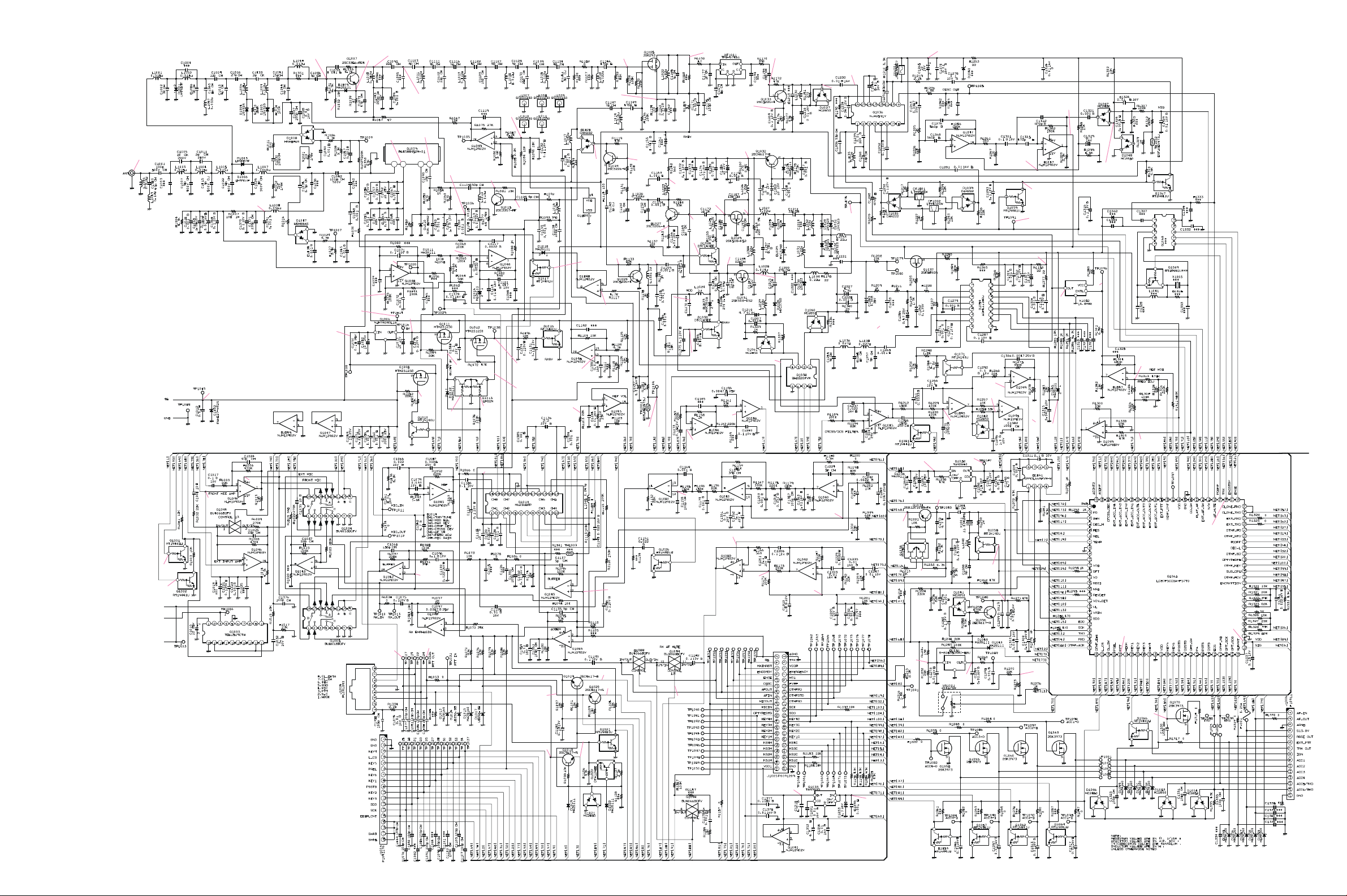
MAIN Unit (Lot 1~4)
Circuit Diagram
RX:1.3V
TX:0V
AF OFF:5.0V
AF ON:0V
5.0V
13.6V
2.2V
5.2V
HOOK ON:5.1V
HOOK OFF:0.3V
4.4V
2.2V
RX:5.1V
TX:0V
RX:0V
TX:5.0V
RX:8.1V
TX:0.4V
RX:2.0V
TX:0.4V
5.2V
RX:8.1V
TX:0V
RX:0V
TX:8.1V
RX:5.1V
TX:0V
RX:3.6V
TX:4.4V
2.2V
5.0V
5.0V
2.2V
4.5V
@25°C
RX:0V
TX:8.1V
2.2V
1.1V
MUTE:0V
UNMUTE:5.0V
2.1V
5.2V
2.1V
5.2V
2.2V
1.1V
13.6V
7.7V
12.9V
5.1V
5.2V
RX:1.3V
TX:0.4V
5.6V
5.0V
RX:1.3V
TX:0.4V
2.2V
SHIFT ON:0.1V
SHIFT OFF:3.4V
5.0V
5.2V
LOCK:5.1V
UNLOCK:0V
POW OFF:0V
POW ON:5.6V
RX:5.1V
TX:0V
1.8V
RX:0.8V
TX:0V
RX:0V
TX:5.0V
RX:0V
TX:5.0V
5.0V
(
UHF) Service Manaul
5.1V
5.0V
3.5V
8.1V
H-1VX-2100/-2200

MAIN Unit (Lot 1~4)
Note
H-2 VX-2100/-2200
(
UHF) Service Manaul
MAIN Unit (Lot 1~4)
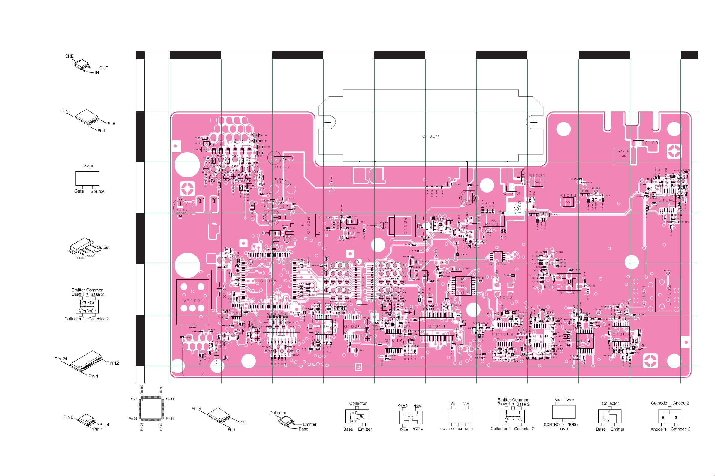
Parts Layout (Side A)
NJM7808DL1A
(Q1006)
BU4053BCFV
(Q1004, 1005)
MTM231230L (BL)
(Q 1008, 1011, 1012)
2SK397300L
(Q1050, 1055, 1060,
1063, 1070)
BA DCEFHGIJ
K
1
2
RA45H4452M
(Q1009)
UMG2N
(Q1013)
M62364FP
(Q1014)
3
4
5
6
BH2220FVM
(Q1034)
BR93L66RFVM
(Q1061)
(
UHF) Service Manaul
LC87F5CC8A
(Q1065)
NJM12902V
(Q1040, 1042, 1043,
1045, 1046, 1048,
1049)
2SB1201S-TL
(Q1039)
RT1N441U (N3)
(Q 1016, 1017, 1026,
1041, 1053, 1057,
1062, 1064, 1067)
3SK293 (UF)
(Q1025)
TAR5S35 (3V5)
(Q1035)
XN1501 (R5)
(Q1038)
TAR5S50
(Q1052)
RT1N140U
(Q1058)
HSM88AS (C1)
(D1007, 1008)
MC2850 (A7)
(D1042, 1060, 1061)
H-3VX-2100/-2200
 Loading...