

Verterx Standard VX-1400 Series Service Manual

VERTEX STANDARD CO., LTD.
4-8-8 Nakameguro, Meguro-Ku, Tokyo 153-8644, Japan
VERTEX STANDARD
US Headquarters
VX-1400 Series
HF Multi Mode Mobile Radio
Service Manual
©2009 VERTEX STANDARD CO., LTD. EC091H90A
10900 Walker Street, Cypress, CA 90630, U.S.A.
YAESU UK LTD.
Unit 12, Sun Valley Business Park, Winnall Close
Winchester, Hampshire, SO23 0LB, U.K.
VERTEX STANDARD HK LTD.
Unit 5, 20/F., Seaview Centre, 139-141 Hoi Bun Road,
Kwun Tong, Kowloon, Hong Kong
VERTEX STANDARD (AUSTRALIA) PTY., LTD.
Normanby Business Park, Unit 14/45 Normanby Road
Notting Hill 3168, Victoria, Australia
Introduction
This manual provides the technical information necessary for
servicing the VX-1400 HF Transceiver.
Servicing this equipment requires expertise in handing surface-mount chip components. Attempts by non-qualified persons to service this equipment may result in permanent damage not covered by the warranty, and may be illegal in some
countries.
Two PCB layout diagrams are provided for each double-sided
board in this transceiver. Each side of the board is referred to
by the type of the majority of components installed on that side (“Side A” or “Side B”). In most cases one side
has only chip components (surface-mount devices), and the other has either a mixture of both chip and leaded
components (trimmers, coils, electrolytic capacitors, ICs, etc.), or leaded components only.
As described in the pages to follow, the advanced microprocessor design of the VX-1400 Transceiver allows a
complete alignment of this transceiver to be performed without opening the case of the radio; all adjustments
can be performed from the front panel, using the “Alignment Mode” menu.
While we believe the information in this manual to be correct, VERTEX STANDARD assumes no liability for
damage that may occur as a result of typographical or other errors that may be present. Your cooperation in
pointing out any inconsistencies in the technical information would be appreciated.
Important Note
1) This transceiver was assembled using Pb (lead) free solder, based on the RoHS specification.
Only lead-free solder (Alloy Composition: Sn-3.0Ag-0.5Cu) should be used for repairs performed on this apparatus. The
solder stated above utilizes the alloy composition required for compliance with the lead-free specification, and any solder
with the above alloy composition may be used.
2) Risk of explosion if battery is replaced by an incorrect type. Dispose of used batteries according to the instructions.
Contents
Specifications ...................................................................................................................................................... 2
Exploded View & Miscellaneous Parts .......................................................................................................... 3
Block Diagram.....................................................................................................................................................5
Connection Diagram ..........................................................................................................................................6
Alignment ............................................................................................................................................................ 7
Board Units (Schematics, Layouts & Parts)
PANEL Unit ................................................................................................................................................ 15
MAIN Unit .................................................................................................................................................. 23
PA Unit ........................................................................................................................................................ 47
ALE-2 Unit (Option) .................................................................................................................................. 59
1VX-1400 Series Service Manual

Specifications
General
Frequency Range: RX: 30 kHz - 30 MHz, TX: 1.6 - 30 MHz
Number of Channel: 512
Emission Modes: A1A (CW), J3E (LSB/USB),A3E (AM), H3E (2182 kHz only),
J2B (FSK/AFSK)
Synthesizer Steps: 10 Hz
Antenna Impedance: 50 Ohm, Unbalanced
Operating Temperature Range: -20° C to +60° C
Frequency Stability: ±0.5 ppm
Power Requirements: DC 13.8V±15 %
Current Consumption: Receive (No Signal) 1 A, Transmit (Max) 23 A
IP Rating: IP54 Front Panel (Only with MH-77 connected)
Case Size (W x H x D): 178 x 60 x 268 mm (7" x 2.4" x 10.6") w/o knobs and fans
Weight (approx.): 3.4 kg (7.5 lbs)
Receiver
Circuit Type: Double Conversion Superheterodyne
Sensitivity (10 dB S/N): J2B/J3E/A1A
0.5 - 1.6 MHz 0.71 µV
1.6 - 30 MHz 0.16 µV
A3E
0.5 - 1.6 MHz 7.93 µV
1.6 - 30 MHz 1.00 µV
Adjacent Channel Selectivity: 2.2 kHz/4.5 kHz (J2B/J3E/A3E Narrow)
(-6 dB / -60 dB) 500 Hz / 1.2 kHz (A1A Narrow)
6 kHz / 20 kHz (A3E)
IF Rejection: 80 dB (1.8 - 30 MHz)
Image Rejection: 80 dB (1.8 - 30 MHz)
Audio Output: 10 W into 4 Ohm @ 5% THD (J3E/A1A)
Transmitter
Power Output (@13.8 V, 25° C): 100 W (J2B/J3E/A1A),
Low/Mid/High, 3 steps selectable the setting power is adjustable by
1 W step (100 W - 10W)
25 W AM Carrier (A3E/H3E) (25 W - 2.5W)
Modulation Type: PSN Type Modulator (SSB),
Low-Level (Early Stage) (AM)
Spurious Radiation (Harmonics): -42 dB (1.8 - 30 MHz)
-36 dB (1.6 - 1.8 MHz,)
J3E Carrier Suppression: -45 dB @ 100 W (PEP)
Undesired Sideband Suppression: 50 dB @ 1.5 kHz tone, 100 W (PEP)
SSB Audio Response: < -6 dB (300 to 2400 Hz)
Occupied Bandwidth: < 0.5 kHz (A1A)
< 3.0 kHz (J2B/J3E/H3E)
< 6.0 kHz (A3E)
Microphone Impedance: 200 Ohm - 10 k-Ohm, (600 Ohm: Nominal)
Specifications are subject to change without notice or obligation.
2 VX-1400 Series Service Manual
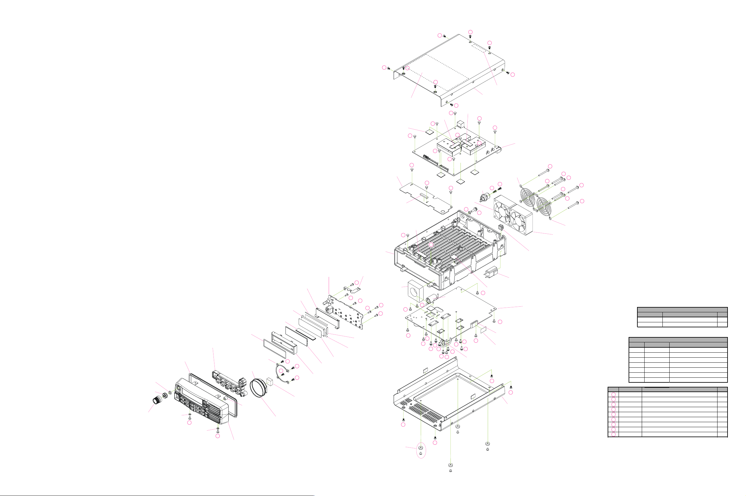
Exploded View & Miscellaneous Parts
4
RA1147800
SHIELD PLATE
SPONGE RUBBER
RA1143400
CHASSIS
RA1205100
SHEEET
RA118680A
PAD
(x4pcs)
RA1193400
RA1198800
PORON SHEET
4
3
PORON SHEET
7
7
4
4
RA1198800
7
7
7
3
4
7
7
7
4
PORON SHEET
7
P1091172
CONNECTOR
M2090029
FAN
9
RA1143500
TOP CASE
RA1198800
7
7
8
4
4
S5000320
FAN GUARD
7
RA0471500
ELEC. COND TAPE(C)
7
7
MAIN UNIT
2
2
M2090029
RA1162400
RUBBER COVER
2
2
2
2
S5000320
FAN GUARD
FAN
2
2
R6054387B
SPECIAL NUT
RA1130600
RUBBER PACKING
RA1130300
VOLUME KNOB
RA0913400
RUBBER PACKING
RA0940400
O RING
RA1130500
RUBBER KNOB
3
RA0940400
O RING
RUBBER CONNECTOR (LCD)
SPONGE RUBBER (LCD)
RA1142700
M4090200
SPEAKER
RA1146900
3
(W/ SP NET, LED GUIDE, WINDOW)
REFLECTOR SHEET(B)
LIGHT GUIDE (LCD)
RA1130800
RA1167100
SP HOLDER
RUBBER
RUBBER PACKING
RA1139800
HOLDER (LCDGUIDE)
RA1207400
RA113790A
5
5
5
5
RA1198900
RA1130700
RA1129900
PANEL ASSY
PANEL UNIT
G6090199
RA1130900
LCD HOLDER
TERMINAL PLATE
6
6
REFLECTOR SHEET(A)
REFLECTOR SHEET(C)
RA116700A
DIFFUSER SHEET
LCD
RA1159000
SPONGE RUBBER
6
6
RA1207300
RA1207500
RA1205000
6
6
S4000055
CASE LEG
(x4 pcs)
T9207485
RUBBER COVER
RA0544700
PAD
7
L9190115
FERRITE BEADS
RA1179800
DOUBLE FACE
4
4
BOTTOM CASE
PA UNIT
RA1143600
REF.
1
2
3
4
5
6
7
8
9
REF.
P 0001
P 0002
P 0003
P 0004
P 0005
P 0006
P 0007
VXSTD P/N
U03308002
U04335007
U20306027
U31306007
U23206001
U23208001
U24306001
U9900076
U72004002
VXSTD P/N
T9025225
Q0000074
T9317982
T9318227A
T9207114A
T9207484A
T9207485
T9207511
T9207512
SEMS SCREW
SEMS SCREW
BINDING HEAD SCREW
OVAL HEAD SCREW
BIND HEAD TAPTITE-P
BIND HEAD TAPTITE-P
BIND HEAD TAPTITE-B
HEX SOCKET BOLT
TOOTHED LOCK WASHER
SUPPLIED ACCESSORIES
DC Power Cord
Spare Fuse (25 A Blade Type)
CONNECTION CABLES
VXSTD P/N
WIRE ASSY (J4001 J5008
WIRE ASSY (J4002 J5002
WIRE ASSY (J4003 J5003
WIRE ASSY (J4004 J3001
WIRE ASSY (13.5V/GND
WIRE ASSY (J4011 J5006
WIRE ASSY (J3002 Speaker
DESCRIPTION
DESCRIPTION
DESCRIPTION
ASM3X8NI
HSM3X35B
M3X6SUS B
M3X6B
M2.6X6
M2.6X8
M3X6
HSM4X16NI
OW4NI
QTY.
1
2
)
)
)
)
)
)
)
QTY.
7
8
4
12
4
6
24
1
1
1
1
RA1179900
7
7
TUBE
RA1179900
7
7
7
7
7
1
1
4
4
TUBE
7
1
1
1
7
VX-1400 Series Service Manual
Non-designated parts are available only as part of a designated assembly.
3

Exploded View & Miscellaneous Parts
Note
4
VX-1400 Series Service Manual

Block Diagram
VX-1400 Series Service Manual
5
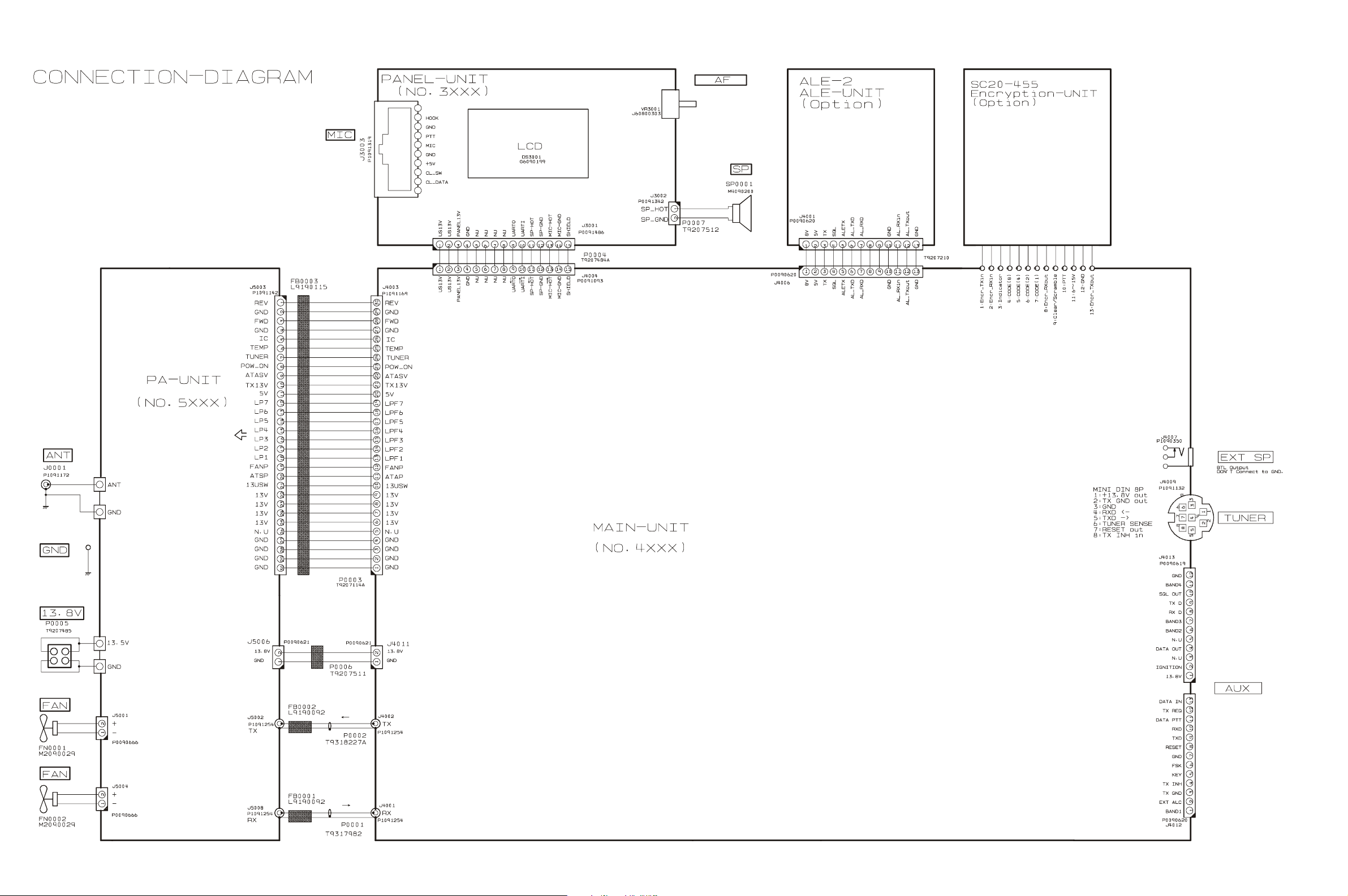
Connection Diagram
6
VX-1400 Series Service Manual

Alignment
Introduction and Precautions
The following procedures cover adjustments that are not
normally required once the transceiver has left the factory. However, if a problem occurs during normal operation due to component failure; realignment may be required after the faulty components have been replaced.
We recommend that authorized Vertex Standard Technicians, who are experienced with the circuitry and fully
equipped to repair and align our products, perform repairs. If a fault is suspected, contact the selling dealer for
instructions regarding repair. Authorized Vertex Standard
Technicians have the latest information to align all circuits and make complete performance checks to ensure
compliance with factory specifications after repairs.
Those who undertake the following alignments are cautioned to proceed at their own risk. Problems caused by
unauthorized attempts at realignment are not covered by
the warranty policy.
Vertex Standard must reserve the right to change circuits
and alignment procedures in the interest of improved
performance, without notifying owners.
Under no circumstances should any alignment be attempted unless the normal functions and operation of the
transceiver are clearly understood, the cause of the malfunction has been clearly identified and all faulty components replaced. The need for realignment should be determined to be necessary.
The following test equipment (and a thorough familiarity with its correct use) is necessary for correct alignment.
Most steps do not require all of the equipment listed. The
interactions of some adjustments may require that several adjustments be performed in a sequence. Do not attempt to perform only a single step unless it is clearly
isolated electrically from all other steps. Have all test
equipment ready before beginning, and follow all of the
steps in a section in the order they are presented.
Required Test Equipment
RF Signal Generator
AF Signal Generator
Spectrum Analyzer good to at least 1 GHz.
Frequency Counter
RF Millivoltmeter
Digital DC Voltmeter (high-Z, 1 M-Ohm/V)
DC Voltmeter
DC Ammeter (20 A)
Ohmmeter
50-Ohm Dummy Load (150 watts)
150-Ohm Dummy Load (150 watts)
In-Line Wattmeter (100 watts, 50-Ohm)
RF Sampling Coupler
4-Ohm AF Dummy Load (15 watts)
IBM® PC / compatible Computer with Windows
Vista/XP/2000
Vertex Standard VPL-1 or FIF-10 + CT-104A Pro-
gramming Cable & CE111 Programming Software
Alignment Preparation & Precautions
A 50-ohm RF Dummy load and in-line wattmeter must
be connected to the "ANT" jack in all procedures that call
for transmission, except where specified otherwise. Correct alignment is not possible with an antenna.
After completing one step, read the following step to determine whether the same test equipment will be required.
If not, remove the unneeded test equipment before proceeding (except the dummy load and wattmeter).
Correct alignment requires that the ambient temperature
be maintained constant between 68 °F ~ 86 °F (20 °C ~ 30
°C). When the transceiver is brought into the shop from a
hot or cold environment, it should be allowed time to come
to room temperature before alignment. Also, the test
equipment must be thoroughly warmed up before beginning.
®
Whenever possible, alignments should be made with oscillator shields and circuit boards firmly affixed in place.
Note: Signal levels in dB referred to in this procedure
are based on 0 dBµ = 0.5 µV (closed circuit).
Caution: Do not connect the audio output line to ground,
and be certain that the speaker has adequate capability to handle the audio output from the
radio.
7VX-1400 Series Service Manual
Alignment
Preparation
Please back up the data of VX-1400 (following refer-
ence).
1. "Upload" function in the "Radio" menu of CE111.
2. Click on the [ON] button.
«
3. "Save As" function in the "File"
menu of CE111.
4. "Save" function in the "File" menu
of CE111.
Please select "VX-1400
Alignment.c111" clicking "File""Open".
Please select "Radio"-"Download" and return it to
former data when the adjustment ends.
50-ohm
Dummy Load
Inline
Wattmeter
Frequency
Counter
RF Sampling
Coupler
ANT
VPL-1 or FIF-10+CT-104A
Programming Cable
COM Port
CE111 Programming Software
Install the CE111 (Clone Editor) to your PC.
Set the "VOL" of VX-1400 to the position of "12-
o'clock".
Connect the VX-1400 to a computer with a Clone cable.
RF
Signal Generator
Transceiver
MIC
INPUT
Power Supply
13.8 VDC
PLL Reference Frequency Alignment
Press and hold in the [P1], [P2], [P0] and [P3] keys,
while turning the radio on, to enter the alignment
mode.
Connect the Frequency Counter to TP4044 on the
MAIN Unit.
Press the [] / [] key for 22.625 MHz ±1Hz on the
Frequency Counter.
Press and hold in the [MENU] button for 2 seconds to
save the new settings and exit from the alignment
mode.
2nd Local Carrier Output Level
Connect the RF millivoltmeter to TP4039 on the MAIN
Unit.
Adjust T4017 on the MAIN Unit for maximum de-
flection on the RF millivoltmeter (more than 40
mVrms).
PLL VCV Voltage
Connect the Digital DC voltmeter (high-Z) to TP4058
on the MAIN Unit.
Referring to the table below, adjust the listed compo-
nents for the required voltage, or confirm that the correct voltage is present on each frequency listed (It does
again).
CH
010
011
012
013
VCO
VCO1
VCO1
VCO2
VCO2
Adjustment
5.2 ± 0.1 V
> 0.6 V
5.2 ± 0.1 V
> 0.6 V
TX IF Circuit (SSB/CW)
Connect the 50-Ohm Dummy Load and Wattmeter to
the "ANT" jack.
Disconnect the TMP plug from J4002 on the RF-IF-
Unit, and then connect the RF millivoltmeter and 50
Ohm dummy load to J4002.
Inject the 1 mV, 1 kHz audio signal to MIC Terminal
of MIC jack.
Press the [ ]/[ ], [] / [ ] button to select the
"memory channel 015".
Press the PTT button; adjust T4015, T4012, T4013,
T4014, and T4011 on the MAIN-Unit for maximum
deflection on the RF millivoltmeter (Please adjust it
again).
Disconnect the RF millivoltmeter and 50 Ohm dummy
load from J4002 on the MAIN-Unit, then re-connect
the TMP plug to J4002.
RX IF Circuit (SSB/CW)
Connect the AF millivoltmeter and 4 Ohm dummy
load to the EXT SPKR jack.
Connect the RF Signal Generator to the "ANT" jack,
8 VX-1400 Series Service Manual
and then set the output level to 0 dBµV at the 19.9
MHz.
Press the [] / [] button to select the "memory chan-
nel 017".
Adjust T4016 on the MAIN-Unit for maximum deflec-
tion on the AF millivoltmeter.
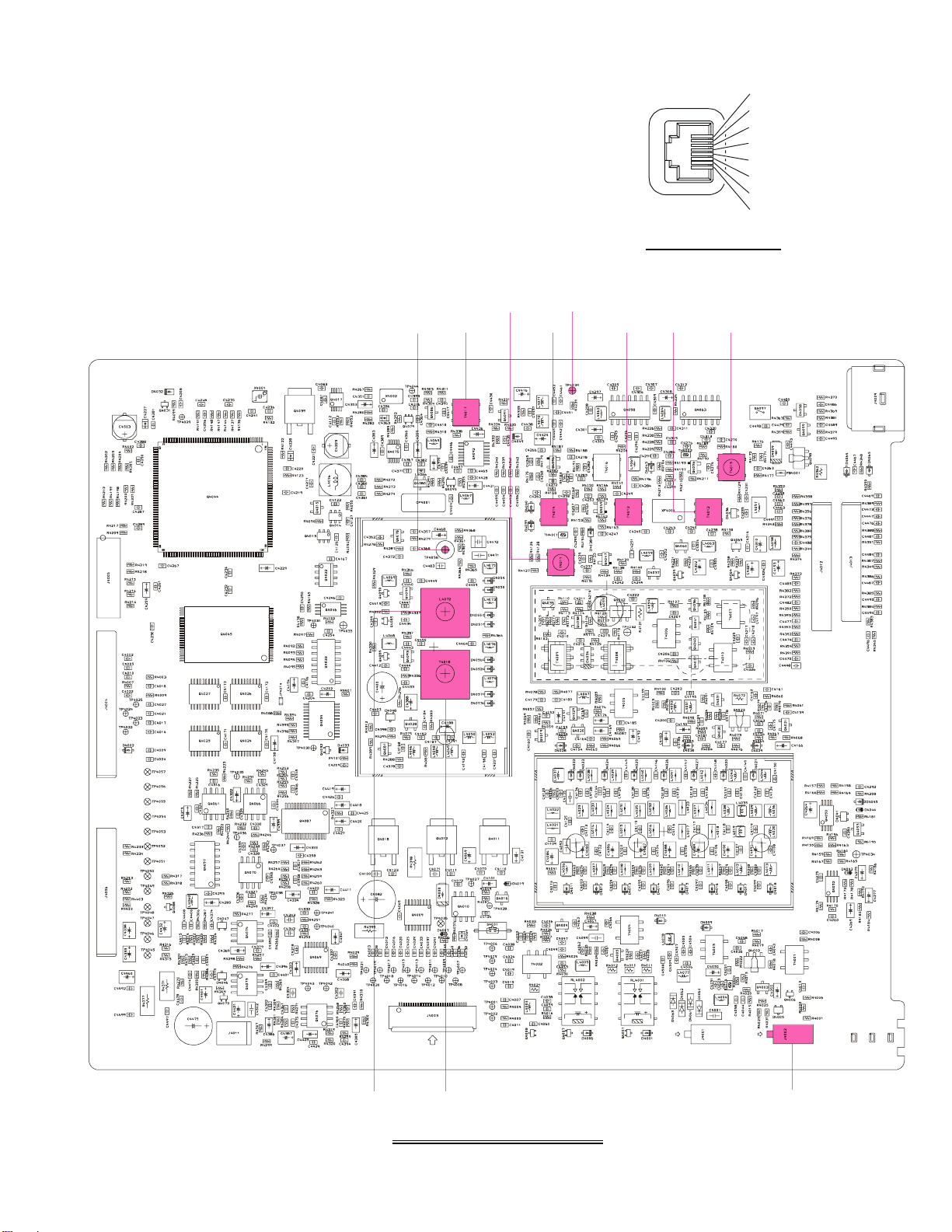
Alignment
CL_DATA
CL_SW
+ 5V
GND
MIC
PTT
GND
HOOK
MIC JACK PINOUT
TP4058
T4011
T4017 T4015T4014 T4013 T4012
TP4039
T4018L4072
MAIN UNIT ALIGNMENT POINTS
J4002
9VX-1400 Series Service Manual

Alignment
PA Unit
Preparation
Connect the 50-Ohm Dummy Load and Wattmeter to
the "ANT" jack.
Disconnect the jumper plug from J5007 and J5005 on
the PA Unit.
Set VR5001, VR5002, VR5003, VR5004 and VR5005 on
the PA Unit to fully counter clockwise position.
Press the [] / [] button to select the "memory chan-
nel 019".
Pre-Drive Stage Idling Current
Disconnect the jumper plug from J5007 and J5005 on
the PA Unit, and then connect the DC ammeter to
J5005.
Press the PTT button; adjust VR5001 on the PA Unit
so the DC ammeter reading is 150 mA ± 10 mA.
Release the PTT button.
Drive Stage Idling Current
Disconnect the jumper plug from J5007 on the PA Unit,
and then connect the DC ammeter to J5007.
Press the PTT button; adjust VR5002 on the PA Unit
so that the DC ammeter reading is 0.5 A ± 50 mA.
Release the PTT button.
Press the PTT button; adjust VR5003 on the PA Unit
so the DC ammeter reading is 1.0 A ± 50 mA.
Release the PTT button.
Final Stage Idling Current
Connect the DC ammeter to the lead of L5008.
Press the PTT button; adjust VR5004 on the PA Unit
so the DC ammeter reading is 1.0 A ± 100 mA.
Release the PTT button.
Press the PTT button; adjust VR5005 on the PA Unit
so the DC ammeter reading is 2.0 A ± 100 mA.
Release the PTT button.
Concluding
Re-connect the jumper plugs to J5005 and J5007, and
then solder the lead of L5008 (It cuts power switch).
CM Coupler Balance
Connect the DC voltmeter between TP5028 (+ lead)
on the PA Unit and Chassis (- lead).
Press the [] / [] button to select the "memory chan-
nel 021".
Press the PTT switch; adjust TC5001 on the PA Unit
for minimum deflection on the DC voltmeter.
Release the PTT switch.
10 VX-1400 Series Service Manual
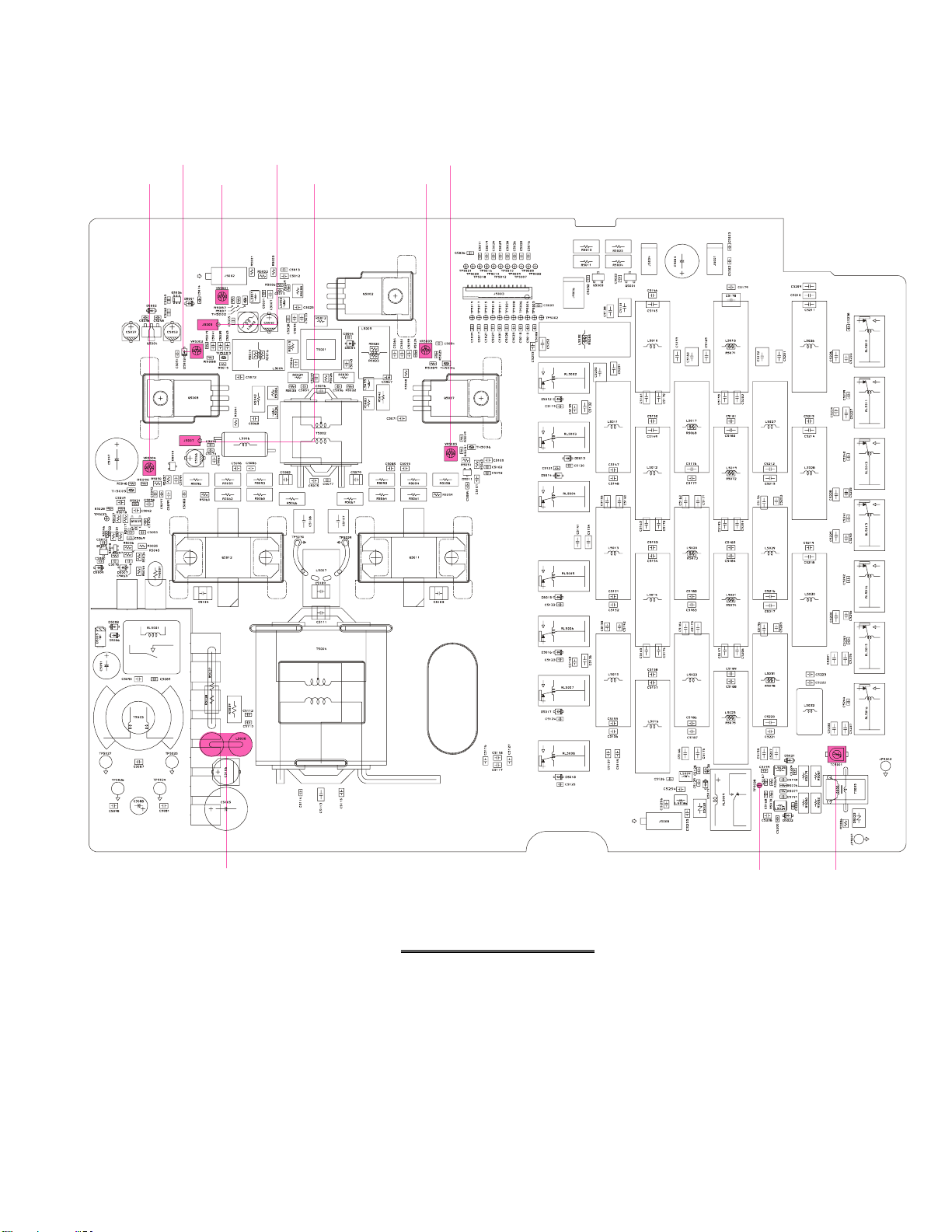
Alignment
VR5004
VR5002
VR5001
J5005
J5007
VR5005
VR5003
L5008
PA U NIT ALIGNMENT POINTS
TP5028
TC5001
11VX-1400 Series Service Manual
Alignment
Software Adjustment
ALC Adjustment
Connect the 50-Ohm Dummy Load and Wattmeter to
the "ANT" jack.
Press and hold in the [P1], [P2], [P0] and [P3] keys,
while turning the radio on, to enter the alignment
mode.
Press the [S2/2182] knob to select the alignment pa-
rameter "I-ALC".
Confirm that the alignment value is "80".
Press and hold in the [MENU] button for 2 seconds to
save the new setting and exit from the alignment
mode.
Power Adjustment
Connect the 50-Ohm Dummy Load and Wattmeter to
the "ANT" jack.
Press and hold in the [P1], [P2], [P0] and [P3] keys,
while turning the radio on, to enter the alignment
mode.
Referring to the Table below, press the [S2/2182]
key (or [S1/ALARM] key) to recall each parameter listed, then key the transmitter and press the
[] / [] key for the required output.
PARAMETER
1PO-H
1PO-MH
1PO-ML
1PO-L
2PO-H
2PO-MH
2PO-ML
2PO-L
3PO-H
3PO-MH
3PO-ML
3PO-L
4PO-H
4PO-MH
4PO-ML
4PO-L
OUTPUT POWER
100 W (± 5 W)
50 W (± 2 W)
25 W (± 2 W)
10 W (± 1 W)
100 W (± 5 W)
50 W (± 2 W)
25 W (± 2 W)
10 W (± 1 W)
100 W (± 5 W)
50 W (± 2 W)
25 W (± 2 W)
10 W (± 1 W)
100 W (± 5 W)
50 W (± 2 W)
25 W (± 2 W)
10 W (± 1 W)
PARAMETER
5PO-H
5PO-MH
5PO-ML
5PO-L
6PO-H
6PO-MH
6PO-ML
6PO-L
7PO-H
7PO-MH
7PO-ML
7PO-L
OUTPUT POWER
100 W (± 5 W)
50 W (± 2 W)
25 W (± 2 W)
10 W (± 1 W)
100 W (± 5 W)
50 W (± 2 W)
25 W (± 2 W)
10 W (± 1 W)
100 W (± 5 W)
50 W (± 2 W)
25 W (± 2 W)
10 W (± 1 W)
TX Gain Adjustment
Connect the 50-Ohm Dummy Load and Wattmeter to
the "ANT" jack.
Connect the Audio Generator to MIC Terminal of the
MIC jack (GND Terminal), then set the output level to
1.5 mV @1 kHz.
Press and hold in the [P1], [P2], [P0] and [P3] keys,
while turning the radio on, to enter the alignment
mode.
Referring to the Table below, press the [S2/2182]
key (or [S1/ALARM] key) to recall each parameter listed, then key the transmitter (connect PTT
Terminal of the MIC jack to GND) and press the
[] / [] key for the required output.
PARAMETER
1TX-G-H
2TX-G-H
3TX-G-H
4TX-G-H
5TX-G-H
6TX-G-H
7TX-G-H
Press and hold in the [MENU] button for 2 seconds to
save the new settings and exit from the alignment
mode.
OUTPUT POWER
50 W (± 10 W)
50 W (± 10 W)
50 W (± 10 W)
50 W (± 10 W)
50 W (± 10 W)
50 W (± 10 W)
50 W (± 10 W)
PARAMETER
1TX-G-L
2TX-G-L
3TX-G-L
4TX-G-L
5TX-G-L
6TX-G-L
7TX-G-L
OUTPUT POWER
5 W (± 2 W)
5 W (± 2 W)
5 W (± 2 W)
5 W (± 2 W)
5 W (± 2 W)
5 W (± 2 W)
5 W (± 2 W)
AM Carrier Level Adjustment
Connect the 50-Ohm Dummy Load and Wattmeter to
the "ANT" jack.
Press and hold in the [P1], [P2], [P0] and [P3] keys,
while turning the radio on, to enter the alignment
mode.
Press the [S2/2182] key (or [S1/ALARM] key) to
select the alignment parameter "AMCAR".
Press the PTT switch without the microphone audio
input, then press the [] / [] key for 25 W±2 W on
the Wattmeter.
Release the PTT switch.
Press and hold in the [MENU] button for 2 seconds to
save the new setting and exit from the alignment
mode.
Press and hold in the [MENU] button for 2 seconds to
save the new settings and exit from the alignment
mode.
CL_DATA
CL_SW
+ 5V
GND
MIC
PTT
GND
HOOK
MIC JACK PINOUT
12 VX-1400 Series Service Manual

Reverse ALC Adjustment
Connect the 150-Ohm Dummy Load to the "ANT" jack.
Press and hold in the [P1], [P2], [P0] and [P3] keys,
while turning the radio on, to enter the alignment
mode.
Press the [S2/2182] key (or [S1/ALARM] key) to se-
lect the alignment parameter "1R-ALC".
Press the PTT switch, then press the [] / [] key for
50 W on the PO meter of the VX-1400.
Release the PTT switch.
RPress the [S2/2182] key (or [S1/ALARM] key) to se-
lect the alignment parameter "2R-ALC".
Press the PTT switch, then press the [] / [] key for
50 W on the PO meter of the VX-1400.
Release the PTT switch.
Press the [S2/2182] key (or [S1/ALARM] key) to se-
lect the alignment parameter "3R-ALC".
Press the PTT switch, then press the [] / [] key for
50 W on the PO meter of the VX-1400.
Release the PTT switch.
Press and hold in the [MENU] button for 2 seconds to
save the new settings and exit from the alignment
mode.
Alignment
13VX-1400 Series Service Manual

Alignment
Note
14 VX-1400 Series Service Manual
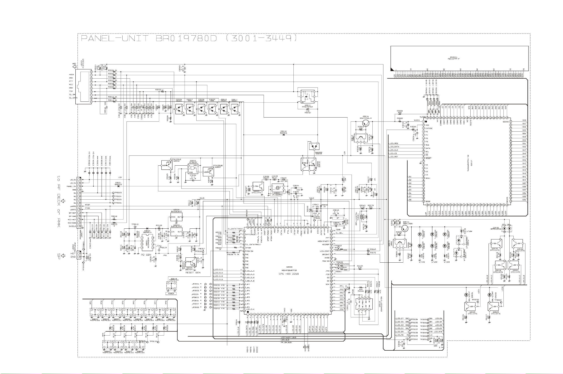
PANEL Unit
Circuit Diagram
VX-1400 Series Service Manual
15

PANEL Unit
Note
16
VX-1400 Series Service Manual

Parts Layout (Side A)
PANEL Unit
A B
1
2
3
C D E
F G
VX-1400 Series Service Manual
DTC114TE (04)
(Q3018, 3019, 3021, 3022)
17
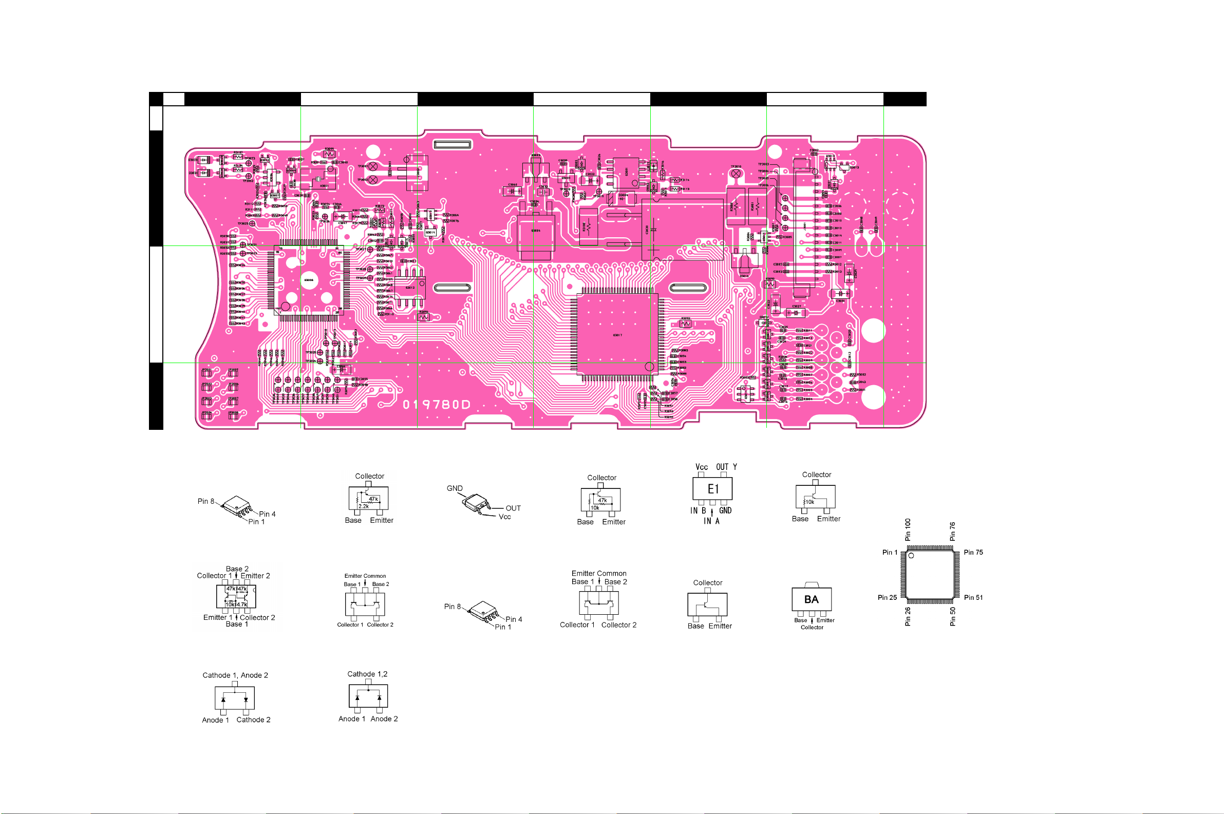
PANEL Unit
Parts Layout (Side B)
a b c d e
f g
1
2
3
18
M51945BFP-CF0R
(Q3001)
UMD5N
(Q3010)
DA221(K)
(D3006, 3008, 3010, 3011)
DTA123JE(E32)
(Q3002, 3007)
RTQ030P02(LE)
(Q3011)
DAN222(N)
(D3013)
BA50BC0FP-E2
(Q3004)
25AA512T-I/SN
(Q3012)
2SC4047(ZY)
(Q3005)
UMW1(W1)
(Q3013, 3015)
TC7S00F(E1)
(Q3006)
2SA1576A(F141)
(Q3014)
DTC114TE
(Q3009, 3020, 3023)
2SB1132(BA)
(Q3016)
HD64F2268TF20
(Q3008)
NJU6624CFG1-02
(Q3017)
VX-1400 Series Service Manual
PANEL Unit
Parts List
DESCRIPTION VALUE V/W TOL. VXSTD P/NMFR’S DESIG VERS.REF. LOT. SIDE
PCB with Components CS2055401
Printed Circuit Board FR019780D 1C 3001 CHIP CAP. 100pF 50V CH GRM1552C1H101JD01D K22178236 1- B b1
C 3002 CHIP CAP. 100pF 50V CH GRM1552C1H101JD01D K22178236 1- B f1
C 3004 CHIP CAP. 100pF 50V CH GRM1552C1H101JD01D K22178236 1- B f1
C 3005 CHIP CAP. 100pF 50V CH GRM1552C1H101JD01D K22178236 1- B f2
C 3007 CHIP CAP. 100pF 50V CH GRM1552C1H101JD01D K22178236 1- B f2
C 3009 CHIP CAP. 100pF 50V CH GRM1552C1H101JD01D K22178236 1- B f1
C 3011 CHIP CAP. 100pF 50V CH GRM1552C1H101JD01D K22178236 1- B f1
C 3014 CHIP CAP. 100pF 50V CH GRM1552C1H101JD01D K22178236 1- B f1
C 3016 CHIP CAP. 100pF 50V CH GRM1552C1H101JD01D K22178236 1- B f3
C 3017 CHIP CAP. 100pF 50V CH GRM1552C1H101JD01D K22178236 1- B f3
C 3018 CHIP CAP. 100pF 50V CH GRM1552C1H101JD01D K22178236 1- B f3
C 3019 CHIP TA.CAP. 22uF 4V TEESVP0G226M8R K78060047 1- B e1
C 3020 CHIP CAP. 100pF 50V CH GRM1552C1H101JD01D K22178236 1- B f2
C 3021 CHIP CAP. 0.001uF 50V B GRM155B11H102KA01D K22178809 1- B f2
C 3022 CHIP TA.CAP. 10uF 10V TEESVA1A106M8R K78100028 1- B f2
C 3023 CHIP CAP. 100pF 50V CH GRM1552C1H101JD01D K22178236 1- B f2
C 3024 CHIP CAP. 100pF 50V CH GRM1552C1H101JD01D K22178236 1- B f2
C 3025 CHIP CAP. 100pF 50V CH GRM1552C1H101JD01D K22178236 1- B f2
C 3026 CHIP CAP. 0.1uF 10V B GRM155B11A104KA01D K22108802 1- B d1
C 3030 AL.ELECTRO.CAP. 1000uF 16V RE3-16V102MH3# K40129096 1- B d1
C 3032 CHIP CAP. 0.1uF 25V B GRM21BB11E104KA01L K22140811 1- B d1
C 3033 CHIP TA.CAP. 1.5uF 16V TEESVA1C155M8R K78120020 1- B d1
C 3034 CHIP CAP. 0.1uF 10V B GRM155B11A104KA01D K22108802 1- B d1
C 3035 CHIP CAP. 0.1uF 10V B GRM155B11A104KA01D K22108802 1- B d1
C 3036 CHIP CAP. 0.1uF 10V B GRM155B11A104KA01D K22108802 1- B a1
C 3038 CHIP CAP. 12pF 50V CH GRM1552C1H120JZ01D K22178214 1- B a1
C 3039 CHIP CAP. 8pF 50V CH GRM1552C1H8R0DZ01D K22178210 1- B b1
C 3040 CHIP CAP. 10pF 50V CH UMK105CH100DV-F K22178258 1- B b1
C 3042 CHIP CAP. 0.22uF 10V B GRM155B31A224KE18D K22108808 1- A F2
C 3043 CHIP CAP. 0.1uF 10V B GRM155B11A104KA01D K22108802 1- B f3
C 3045 CHIP CAP. 0.01uF 25V B GRM155B11E103KA01D K22148834 1- B b1
C 3046 CHIP CAP. 0.01uF 25V B GRM155B11E103KA01D K22148834 1- B b1
C 3047 CHIP TA.CAP. 10uF 10V TEESVA1A106M8R K78100028 1- B b1
C 3048 CHIP CAP. 0.1uF 10V B GRM155B11A104KA01D K22108802 1- B f1
C 3049 CHIP CAP. 100pF 50V CH GRM1552C1H101JD01D K22178236 1- B f1
C 3050 CHIP CAP. 0.1uF 10V B GRM155B11A104KA01D K22108802 1- B b1
C 3051 CHIP CAP. 0.1uF 10V B GRM155B11A104KA01D K22108802 1- B b2
C 3052 CHIP CAP. 0.01uF 25V B GRM155B11E103KA01D K22148834 1- B b1
C 3053 CHIP CAP. 0.1uF 10V B GRM155B11A104KA01D K22108802 1- B e2
C 3054 CHIP CAP. 0.1uF 10V B GRM155B11A104KA01D K22108802 1- B e2
C 3055 CHIP CAP. 0.1uF 10V B GRM155B11A104KA01D K22108802 1- B b3
C 3056 CHIP CAP. 0.1uF 10V B GRM155B11A104KA01D K22108802 1- B e3
C 3057 CHIP CAP. 0.1uF 10V B GRM155B11A104KA01D K22108802 1- B e3
C 3058 CHIP CAP. 0.1uF 10V B GRM155B11A104KA01D K22108802 1- B e3
C 3059 CHIP CAP. 0.1uF 10V B GRM155B11A104KA01D K22108802 1- B d3
C 3060 CHIP TA.CAP. 22uF 6.3V TEESVA0J226M8R K78080047 1- B c1
D 3001 DIODE BAS316 G2070716 1- B f1
D 3002 DIODE BAS316 G2070716 1- B e1
D 3003 LED TLOU1020(T14.F) G2070990 1- A B2
D 3004 DIODE SM240LA-T G2071156 1- B d1
D 3005 DIODE BAS316 G2070716 1- B d1
D 3006 DIODE DA221 TL G2070178 1- B f3
D 3008 DIODE DA221 TL G2070178 1- B f3
D 3010 DIODE DA221 TL G2070178 1- B f2
D 3011 DIODE DA221 TL G2070178 1- B f2
D 3012 DIODE BAS316 G2070716 1- B e2
D 3013 DIODE DAN222 TL G2070174 1- B f1
D 3014 DIODE BAS316 G2070716 1- B b1
D 3015 DIODE BAS316 G2070716 1- B b1
D 3016 LED 67-31A/SAC-AW1X2B9Z5/2T G2071284 1- A A1
D 3017 LED 67-31A/SAC-AW1X2B9Z5/2T G2071284 1- A A1
D 3031 LED SML-210VTT86 G2070768 1- B a1
D 3032 LED BRPG1204W(TAPE) G2070820 1- A F2
D 3033 LED SML-210MTT86 G2070524 1- B a1
D 3034 LED TLOU1020(T14.F) G2070990 1- A C2
D 3035 LED TLOU1020(T14.F) G2070990 1- A D2
D 3036 LED TLOU1020(T14.F) G2070990 1- A E2
D 3037 LED TLOU1020(T14.F) G2070990 1- A F2
D 3038 LED TLOU1020(T14.F) G2070990 1- A F1
LAY ADR
19VX-1400 Series Service Manual

PANEL Unit
Parts List
DESCRIPTION VALUE V/W TOL. VXSTD P/NMFR’S DESIG VERS.REF. LOT. SIDE
DS3001 LCD FE0157TF-F G6090199 1- A D1
J 3001 CONNECTOR 53398-1571 P0091486 1- B f1
J 3002 CONNECTOR B2B-ZR-SM4-TFT(LF)(SN) P0091342 1- B b1
J 3003 CONNECTOR 43090-1505 P1091319 1- A A2
JP3008 CHIP RES. 0 1/16W 5% RMC1/16 000JATP J24185000 EXPORT 1- B a3
Q 3001 IC M51945BFP-CF0R G1091990 1- B d1
Q 3002 TRANSISTOR DTA123JE TL G3070331 1- B a1
Q 3004 IC BA50BC0FP-E2 G1094732 1- B d1
Q 3005 TRANSISTOR 2SC4047-TA G3340477 1- B d1
Q 3006 IC TC7S00F TE85R G1091442 1- B a1
Q 3007 TRANSISTOR DTA123JE TL G3070331 1- B a1
Q 3008 IC HD64F2268TF20(FLASH) G1094580 1- B b2
Q 3009 TRANSISTOR DTC114TE TL G3070225 1- B a1
Q 3010 TRANSISTOR UMD5N TR G3070343 1- B f1
Q 3011 FET RTQ030P02 G4070015 1- B e3
Q 3012 IC 25AA512T-I/SN G1094726 1- B b2
Q 3013 TRANSISTOR UMW1 TR G3070078 1- B c1
Q 3014 TRANSISTOR 2SA1576A T106 R G3115768R 1- B c1
Q 3015 TRANSISTOR UMW1 TR G3070078 1- B e1
Q 3016 TRANSISTOR 2SB1132 T100 Q G3211327Q 1- B e2
Q 3017 IC NJU6624CFG1-02 G1094702 1- B d2
Q 3018 TRANSISTOR DTC114TE TL G3070225 1- A F2
Q 3019 TRANSISTOR DTC114TE TL G3070225 1- A F2
Q 3020 TRANSISTOR DTC114TE TL G3070225 1- B a1
Q 3021 TRANSISTOR DTC114TE TL G3070225 1- A F2
Q 3022 TRANSISTOR DTC114TE TL G3070225 1- A F2
Q 3023 TRANSISTOR DTC114TE TL G3070225 1- B a1
R 3001 CHIP RES. 100k 1/16W 0.5% RR0510R-104-D J24189167 1- B f3
R 3002 CHIP RES. 100k 1/16W 0.5% RR0510R-104-D J24189167 1- B f3
R 3003 CHIP RES. 47k 1/16W 5% RMC1/16S 473JTH J24189045 1- B b2
R 3004 CHIP RES. 1k 1/16W 5% RMC1/16S 102JTH J24189025 1- B f3
R 3005 CHIP RES. 1k 1/16W 5% RMC1/16S 102JTH J24189025 1- B f3
R 3006 CHIP RES. 0 1/16W 5% RMC1/16S JPTH J24189070 1- B f3
R 3007 CHIP RES. 1k 1/16W 5% RMC1/16S 102JTH J24189025 1- B f3
R 3008 CHIP RES. 0 1/16W 5% RMC1/16S JPTH J24189070 1- B f2
R 3009 CHIP RES. 0 1/16W 5% RMC1/16S JPTH J24189070 1- B f2
R 3010 CHIP RES. 1k 1/16W 5% RMC1/16S 102JTH J24189025 1- B f2
R 3011 CHIP RES. 1k 1/16W 5% RMC1/16S 102JTH J24189025 1- B f2
R 3012 CHIP RES. 0 1/16W 5% RMC1/16S JPTH J24189070 1- B f2
R 3013 CHIP RES. 0 1/16W 5% RMC1/16S JPTH J24189070 1- B f2
R 3014 CHIP RES. 47k 1/16W 5% RMC1/16S 473JTH J24189045 1- B b2
R 3015 CHIP RES. 15k 1/16W 5% RMC1/16S 153JTH J24189039 1- B e1
R 3016 CHIP RES. 2.2k 1/16W 1% RMC1/16 222FTP J24183222 1- B e1
R 3017 CHIP RES. 47k 1/16W 5% RMC1/16S 473JTH J24189045 1- B b2
R 3020 CHIP RES. 47k 1/16W 5% RMC1/16S 473JTH J24189045 1- B b2
R 3021 CHIP RES. 47k 1/16W 5% RMC1/16S 473JTH J24189045 1- B b2
R 3022 CHIP RES. 10 1/16W 5% RMC1/16S 100JTH J24189001 1- B f2
R 3023 CHIP RES. 47k 1/16W 5% RMC1/16S 473JTH J24189045 1- B b2
R 3024 CHIP RES. 0 1/16W 5% RMC1/16S JPTH J24189070 1- B f2
R 3025 CHIP RES. 47k 1/16W 5% RMC1/16S 473JTH J24189045 1- B a1
R 3026 CHIP RES. 47k 1/16W 5% RMC1/16S 473JTH J24189045 1- B a1
R 3027 CHIP RES. 47k 1/16W 5% RMC1/16S 473JTH J24189045 1- B d1
R 3028 CHIP RES. 47k 1/16W 5% RMC1/16S 473JTH J24189045 1- B d1
R 3029 CHIP RES. 47k 1/16W 5% RMC1/16S 473JTH J24189045 1- B a1
R 3030 CHIP RES. 47k 1/16W 5% RMC1/16S 473JTH J24189045 1- B a1
R 3034 CHIP RES. 4.7k 1/16W 5% RMC1/16S 472JTH J24189033 1- B a2
R 3035 CHIP RES. 47k 1/16W 5% RMC1/16S 473JTH J24189045 1- B a2
R 3036 CHIP RES. 47k 1/16W 5% RMC1/16S 473JTH J24189045 1- B a2
R 3037 CHIP RES. 47k 1/16W 5% RMC1/16S 473JTH J24189045 1- B a2
R 3038 CHIP RES. 47k 1/16W 5% RMC1/16S 473JTH J24189045 1- B a2
R 3039 CHIP RES. 47k 1/16W 5% RMC1/16S 473JTH J24189045 1- B a2
R 3040 CHIP RES. 47k 1/16W 5% RMC1/16S 473JTH J24189045 1- B a2
R 3041 CHIP RES. 47k 1/16W 5% RMC1/16S 473JTH J24189045 1- B a2
R 3042 CHIP RES. 47k 1/16W 5% RMC1/16S 473JTH J24189045 1- B a2
R 3043 CHIP RES. 1k 1/16W 5% RMC1/16S 102JTH J24189025 1- B a1
R 3044 CHIP RES. 1k 1/16W 5% RMC1/16S 102JTH J24189025 1- B a2
R 3045 CHIP RES. 1k 1/16W 5% RMC1/16S 102JTH J24189025 1- B a2
R 3046 CHIP RES. 1k 1/16W 5% RMC1/16S 102JTH J24189025 1- B a2
R 3047 CHIP RES. 1k 1/16W 5% RMC1/16S 102JTH J24189025 1- B a2
R 3048 CHIP RES. 100 1/16W 5% RMC1/16S 101JTH J24189013 1- B a2
R 3049 CHIP RES. 1k 1/16W 5% RMC1/16S 102JTH J24189025 1- B a1
LAY ADR
20 VX-1400 Series Service Manual
 Loading...