

Page 1

F282x
FOM II Series
Fiber Optic Modem
Technical Manual
February 1999
Revision C
Copyright February 1999
VERSITRON
83 Albe Drive / Suite C
Newark, DE 19702
www.versitron.com
Page 2

PROPRIETARY DATA
All data in this manual is proprietary and may not be disclosed,
used or duplicated, for procurement or manufacturing purposes,
without prior written permission by
VERSITRON, Inc
.
WARRANTY
All VERSITRON products are warranted against defects in materials and workmanship for one year
from date of delivery. We will repair or, at our option, replace parts which during normal usage
prove to be defective during the warranty period provided that:
1. You call VERSITRON at (800) 537-2296 and obtain a Return Authorization Number. This number
must be referenced on the box the item is shipped in.
2. Shipping charges are pre-paid.
No other warranty is expressed or implied and we are not liable for consequential damages. For
repairs outside of the warranty period, the same procedure must be followed.
ii
www.versitron.com
Page 3

TABLE OF CONTENTS
PARAGRAPH TITLE PAGE
SECTION 1: DESCRIPTION OF EQUIPMENT
1.1 INTRODUCTION........................................................................................................... 1
1.2 DESCRIPTION OF EQUIPMENT................................................................................. 1
1.2.1 FUNCTIONAL CHARACTERISTICS .......................................................................... 1
1.2.2 PHYSICAL CHARACTERISTICS ................................................................................ 1
1.3 SPECIFICATIONS ......................................................................................................... 4
SECTION 2: INSTALLATION
2.1 GENERAL ...................................................................................................................... 5
2.2 SITE SELECTION.......................................................................................................... 5
2.3 POWER REQUIREMENTS ........................................................................................... 5
2.4 SWITCH SETTINGS...................................................................................................... 5
2.5 TIMING MODE.............................................................................................................. 7
2.5.1 SOURCE TIMING.......................................................................................................... 7
2.5.2 TERMINAL TIMING ..................................................................................................... 7
2.5.3 INTERNAL TIMING...................................................................................................... 8
2.6 LOOPBACK ................................................................................................................... 9
2.6.1 FIBER/COPPER LOOPBACK....................................................................................... 9
2.6.2 REMOTE/LOCAL LOOPBACK.................................................................................... 9
2.7 INITIAL CHECKOUT PROCEDURE ........................................................................... 9
SECTION 3: OPERATION
3.1 INTRODUCTION........................................................................................................... 10
3.2 STATUS INDICATORS/AUDIBLE ALARM............................................................... 10
3.3 OPERATING CONTROLS ............................................................................................ 10
SECTION 4: THEORY OF OPERATION
4.1 INTRODUCTION........................................................................................................... 11
SECTION 5: MAINTENANCE AND TROUBLESHOOTING
5.1 INTRODUCTION........................................................................................................... 12
5.2 FAULT ISOLATION...................................................................................................... 12
iii
www.versitron.com
Page 4

LIST OF ILLUSTRATIONS
FIGURE TITLE PAGE
1. OVERALL VIEW, F282X MODEM.................................................................................. 2
2. INTERFACE EXTENDER CONFIGURATION ............................................................... 2
3. MODEM LINK CONFIGURATION.................................................................................. 3
4. SWITCH SETTINGS.......................................................................................................... 6
5. INTERNAL TIMING MODES........................................................................................... 8
LIST OF TABLES
TABLE TITLE PAGE
1. ENCLOSURES / CHASSIS................................................................................................ 3
2. SWITCH 3 SETTINGS FOR INTERNAL TIMING.......................................................... 6
3. MODEL F282X SWITCH SETTINGS............................................................................... 7
4. NON-OPERATIONAL INDICATORS .............................................................................. 12
iv
www.versitron.com
Page 5
DESCRIPTION OF EQUIPMENT
1.1 INTRODUCTION
This manual provides general and detailed information on the installation and operation of the
Model F282X FOM II Series Fiber-optic Modems. Section 1 contains a general description of the
equipment. Section 2 covers installation instructions. Section 3 contains operating instructions. Section
4 provides the theory of operation. Section 5 contains maintenance and troubleshooting information.
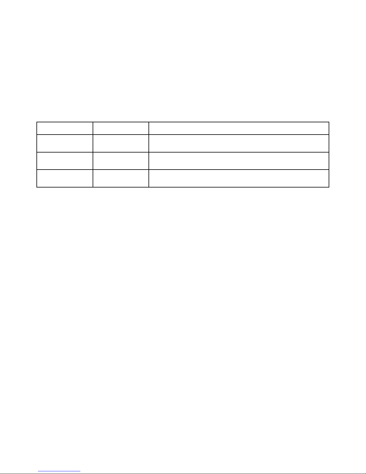
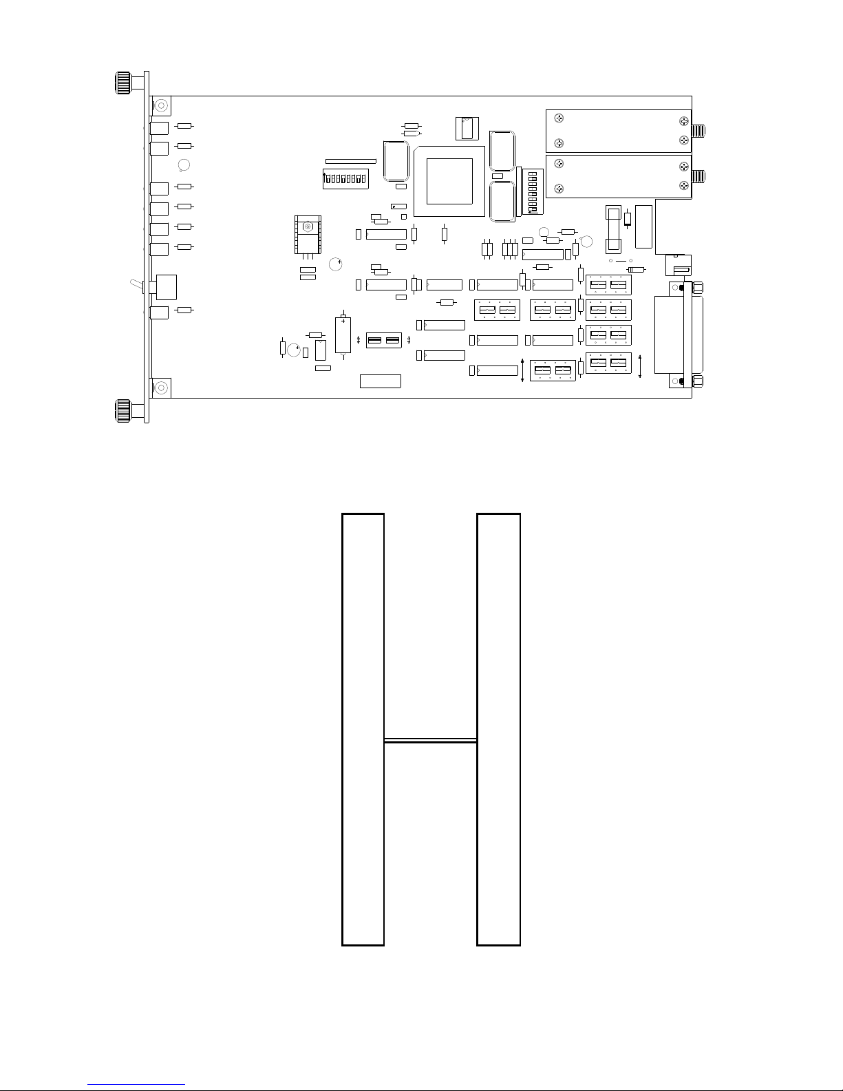
Figure 1 is an overall view of the Model F282X products.
Model Number Part Number Description
F2822 19932-02
F2824 19932-04
F2825 19932-05
1.2 DESCRIPTION OF EQUIPMENT
1.2.1 Functional Characteristics
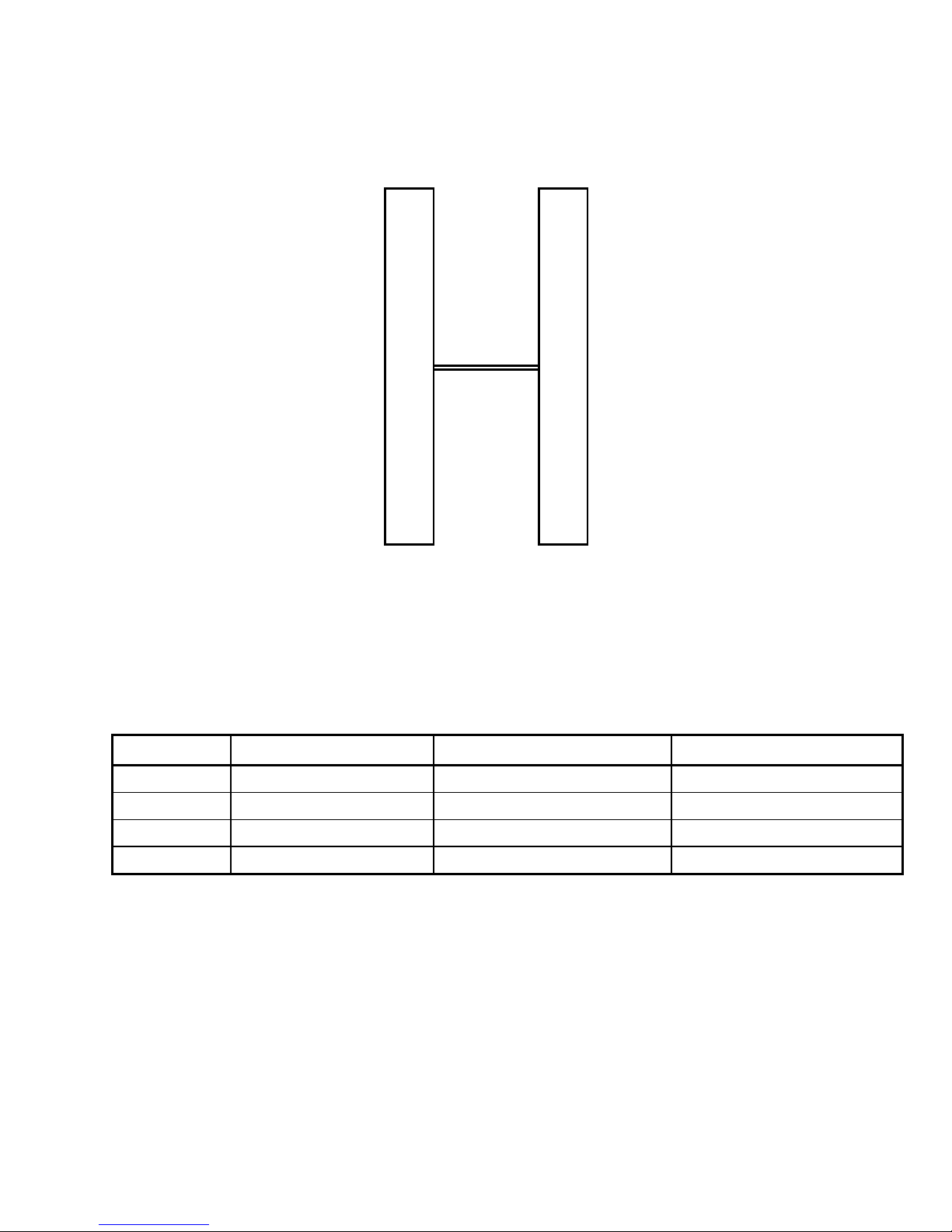
The Model F282X products are fiber-optic links designed for use as an RS-530 interface
extender (See Figure 2) or a modem link (See Figure 3). These units are DTE/DCE switch selectable
and interface with other VERSITRON FOM II series F282X Fiber Optic Modems. Model F2822 uses
multimode fiber-optic cable of up to 2 Km (6,560 ft.), Model F2824 uses multimode fiber optic cable of
up to 6 Km (19,680 ft.) and Model F2825 uses single mode fiber optic cable of up to 14 Km (45,920 ft.).
The link has a maximum data rate of 76.8 Kbps, providing synchronous, asynchronous or isochronous
full-, half-duplex, or simplex data transmission with fully transparent operation. The unit has internal
clock generation for 18 set frequencies. The Model F282X FOM II modems fully support the interface
control signals associated with the EIA RS-530 and MIL-STD-188-114 standards. This is accomplished
by multiplexing the control signals along with clock and data signals and transmitting this serialized
signal to the remote unit. At the remote unit the signal is demultiplexed and applied to the interface.
1.2.2 Physical Characteristics
The Model F282X FOM II products measure 7.0" wide x 0.84" high x 11.6" deep and are
designed to be placed in a variety of VERSITRON enclosures and chassis (see Table 1 for dimensions of
enclosures and chassis). "Desktop" options include both single- and dual-card enclosures. Rack-mount
options include a 2-card and 20-card chassis. The Unit requires a wall transformer for desktop or 2-card
rack mount operation, with a one-pin connector for electrical input on the back of the card. There is a
female DB25 connector for the RS-530 interface and two ST connectors for the fiber-optic interface,
also on the back of the card. The unit requires a VERSITRON Model AC150W rack-mount power
supply for 20-card operation. Two power supplies are required for redundancy. The unit has seven
indicators: power (PWR), alarm (ALM), transmit data (TXD), receive data (RXD), transmit clock
(TXC), receive clock (RXC), and loopback (LB).
SECTION 1
RS-530, 0-76.8 Kbps, multimode, 850nm, ST connectors,
2 Km operational distance.
RS-530, 0-76.8 Kbps, multimode, 1300nm, ST connectors,
6 Km operational distance.
RS-530, 0-76.8 Kbps, multimode, 1300nm, ST connectors,
14 Km operational distance.
1
www.versitron.com
Page 6
2
4
20
24
3
5
13
6
22
10
12
9
18
21
25
LOCAL MODEM
DTE
DCE
REMOTE MODEM
DS1 R13
DS2
DS3
DS4
DS5
DS6
SW1
R7
+
R14
Q1
R15
R16
R17
R18
R19DS7
R30
1
RN2
ON
0
1 2 3
4 5 6 7 8
1
SW4
1
VR1
C1
C8
C2
+
C4
R6
C3
U6
C7
C11
Y2
C10
C9
C18
U4R9C12
C13
R11
C22
U9
C15
TYPICAL SETTINGS
SW5 THRU SW11
ON
OFF
VERSITRON
MADE IN USA
C28
U3
JP1
01
TP1
R10
R12
C23
C24
DTE
C25
DCE
U16
RX
U13
U17
U14
R20
R28
1 2
Y1
TX
RN1
0
1
8
C14
1
SW3
ON
1
Y3
Q2 R5
S
R3
R1
D
C5
R29
R2
1 2
SW5
1 2
R4
C6
R24
R27
R26
U1
R22
C21
U18
C20
U12
DTE
SW10
DCE
CR1F1 P1
Q3
FGND
R23
GND
1
1 2
1
1
SW7
J3
CR3
2
J4
1
14
SW8
SW6
2
SW9
DTE
2
13 25
DCE
1
R8
R21
C19
U15
R25
SW11
U20
C26
U19
C27
FIGURE 1. OVERALL VIEW, F282X MODEMS
Transmit Data +
<<<<---
Transmit Data − <<<<--Request to Send +
<<<<---
Request to Send − <<<<--Data Terminal Ready +
<<<<---
Data Terminal Ready − <<<<--Transmit Clock (TT) +
<<<<---
Transmit Clock (TT) − <<<<--Receive Data +
--->>>>
Receive Data − --->>>>
Clear to Send +
--->>>>
Clear to Send − --->>>>
Data Set Ready +
--->>>>
Data Set Ready − --->>>>
Signal Ground
Carrier Detect +
----
--->>>>
Carrier Detect − --->>>>
Transmit Clock +
--->>>>
Transmit Clock − --->>>>
Receive Clock +
--->>>>
Receive Clock − --->>>>
Local Loopback
Remote Loopback
Test Mode
Frame Ground
--->>>>
--->>>>
--->>>>
----
2
14 14
4
19 19
20
23 23
24
11 11
3
16 16
5
<<<<
-----------
13
>>>>
fiber cable 22
7
7
8 8
10
15 15
12
17 17
9
18
21
25
1 1
6
Transmit Data +
<<<<--<<<<--- Transmit Data −
Request to Send +
<<<<--<<<<--- Request to Send −
Data Terminal Ready +
<<<<--<<<<--- Data Terminal Ready −
Transmit Clock (TT) +
<<<<--<<<<--- Transmit Clock (TT) −
Receive Data +
--->>>>
--->>>> Receive Data −
Clear to Send +
--->>>>
--->>>> Clear to Send −
Data Set Ready +
--->>>>
--->>>> Data Set Ready −
Signal Ground
---Carrier Detect +
--->>>>
--->>>> Carrier Detect −
Transmit Clock +
--->>>>
--->>>> Transmit Clock −
Receive Clock +
--->>>>
--->>>> Receive Clock −
Local Loopback
<<<<---
Remote Loopback
<<<<---
Test Mode
--->>>>
Frame Ground
----
FIGURE 2. INTERFACE EXTENDER CONFIGURATION
2
www.versitron.com
Page 7
3
5
6
17
19
11
LOCAL MODEM
DCE
DCE
REMOTE MODEM
Receive Data +
Receive Data − <<<<--Clear to Send +
Clear to Send − <<<<--Data Set Ready +
Data Set Ready − <<<<--Receive Clock +
Receive Clock − <<<<--Signal Ground
Transmit Data +
Transmit Data − --->>>>
Request to Send +
Request to Send − --->>>>
Data Terminal Ready +
Data Terminal Ready − --->>>>
Transmit Clock (TT) +
Transmit Clock (TT) − --->>>>
Frame Ground
<<<<---
<<<<---
<<<<---
<<<<---
----
--->>>>
--->>>>
--->>>>
--->>>>
----
2
16 14
4
13 19
20
22 23
24
9 11
7
<<<<
-----------
2 fiber cable 3
14
4 5
13
20
23
24 17
9
1 1
>>>>
16
22
Transmit Data +
<<<<--<<<<--- Transmit Data −
Request to Send +
<<<<--<<<<--- Request to Send −
Data Terminal Ready +
<<<<--<<<<--- Data Terminal Ready −
Transmit Clock (TT) +
<<<<--<<<<--- Transmit Clock (TT) −
7
6
Signal Ground
----
Receive Data +
--->>>>
--->>>> Receive Data −
Clear to Send +
--->>>>
--->>>> Clear to Send −
Data Set Ready +
--->>>>
--->>>> Data Set Ready −
Receive Clock +
--->>>>
--->>>> Receive Clock −
Frame Ground
----
FIGURE 3. MODEM LINK CONFIGURATION
Model Number Dimensions Description Power Supply Required
HF-1
HF-2
HF-2SS
HF-20
1.31" H x 7.12" W x 11.6" D Single Card Standalone Enclosure
2.31" H x 7.12" W x 11.6" D Dual Card Standalone Enclosure
1.72" H x 19" W x 13.75" D
7" H x 19" W x 11.6" D 20-Slot Rack Mount Chassis
2-Slot Rack Mount Chassis PSAC08 (US) or PSAC09 (Eur)
PSAC08 (US) or PSAC09 (Eur)
PSAC08 (US) or PSAC09 (Eur)
AC150W (US & Eur)
TABLE 1. ENCLOSURES / CHASSIS
3
www.versitron.com
Page 8

1.3 SPECIFICATIONS
Data Rate: Any data rate from 50 Bps to 76.8 Kbps; synchronous/asynchronous/isochronous. DTE
source timing applications above 56 Kbps may be dependent upon cable length. Consult factory to
discuss your specific application and configuration requirements.
Operating Mode/Range: Simplex, Half- or Full-duplex operation over fiber-optic cable pair.
Maximum operating range is 2 Km (6,560 ft.) with 850nm optics or 6 Km (19,680 ft.) with 1300nm
optics.
Optical Interface: ST connectors compatible with 50/125 µM, 62.5/125 µM or 100/140 µM fiber-optic
cable for 850nm multimode operation, 62.5/125 µM fiber-optic cable for 1300nm multimode operation
and 8/125 µM, 9/125 µM or 10/125 µM fiber optic cable for 1300nm single mode operation.
Digital Interface: Signal levels and format conform to EIA RS-530 / MIL-STD-188-114. The F282X
has a female DB25 connector for connecting to a terminal, with a gender changer available for
connecting to a modem. The unit is switch-selectable between DCE and DTE operation.
Sample Rate: Control signals are sampled at an 18.75 kHz rate. If an asynchronous data signal is used
instead of a control signal the sample rate will result in 5% distortion at 1 Kbps. Data and clock signals
are sampled at 300 kHz.
Dimensions: 7.0" W x 0.84" H x 11.6" D.
Power Requirements: 120 VAC with available DC wall transformer (VERSITRON Model: PSAC08
US, PSAC09 EUR) providing 12 VDC, 1 A.
Environment: 0° to +50°C (32° to +122°F) operating temperature; up to 95% relative humidity (noncondensing); up to 10,000 feet altitude; storage temperature -40° to +70° C.
4
www.versitron.com
Page 9

2.1 GENERAL
This section contains detailed infordmation on the installation and initial checkout of the Model
F282X FOM II Series Modems. Paragraph 2.2 contains general information on site selection and rack
mounting. Paragraphs 2.3 and 2.4 provide instructions for connecting Model F282X products to your
system and selecting the different options. Paragraph 2.5 has the initial checkout procedures.
2.2 SITE SELECTION
The Model F282X FOM II products are designed to connect to the serial port (DB25 Connector)
of the terminal equipment with a cable (customer supplied). The Modem is designed to be placed in a
VERSITRON Model HF-1 or HF-2 desktop enclosure, or rack mounted in a VERSITRON Model HF2SS or Model HF-20 19-inch standard chassis. The enclosure and chassis dimensions are provided in
Table 1 in the previous section. When placed in a desktop enclosure, space for the transformer must also
be provided.
2.3 POWER REQUIREMENTS
The Model F282X FOM II products are designed to operate from an AC power transformer or a
DC power source with a DC voltage of +12 VDC. Before inserting the power transformer
(VERSITRON Model PSAC08 US, PSAC09 EUR) into an AC power source, the plug should be
connected to the Modem. There are no special tools required. DC power may be used instead of the
power transformer if available. This requires a 2.5 mm socket with the positive voltage on the center
and the common on the concentric using +12 VDC at 1 A.
2.4 SWITCH SETTINGS
There are a number of switches on the circuit card of the Model F282X modem, used to select
between DTE/DCE operation, internal/external clock selection, the internal clock data rate, and several
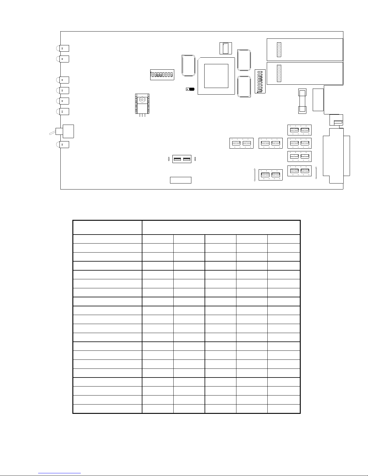
loopback functions. Figure 4 shows the physical location of all of the switches, labeled SW1 through
SW11. With the exception of the loopback switch (SW1), which is on the front panel of the modem
card, all of the switches should be set to the desired position prior to applying power to the modem,
and then left in those positions unless the overall link characteristics change.
Switch 3 (SW3), located between the optical modules and the XILINX field programmable gate
array (FPGA) chip, contains 8 ON-OFF switch positions. The first three positions determine the
interface standard that is expected as an input. Since the complete family of F2800 Series Low-Speed
Modems includes products that operate per the RS-232 standard, there are switch positions for settings
that are irrelevant to the Model F282X products, as they operate only with RS-530 standard inputs. For
the same reason, there is no Switch 2 (SW2) on a Model F282X product. For SW3, Position 2 is set to
ON for DCE operation, and OFF for DTE operation. Positions 1 and 3 must remain OFF.
Positions 4 through 8 of SW3 are used to set the clock rate for internal-timing operation. As listed
in Table 2, there are 18 different clock rates that may be chosen by the settings of SW3, Positions 4
through 8.
SECTION 2
INSTALLATION
5
www.versitron.com
Page 10
DS1
DS2
DS3
DS4
DS5
DS6
SW1
DS7
U16
1
87654321
VERSITRON
MADE IN USA
1
Y2
U3
JP1
0
DTE
DCEOFF
ON
0
1
SW4
VR1
1
TYPICAL SETTINGS
SW5 THRU SW11
ON
Y1
Y3
SW11
RX
TX
10
8
7
6
5
4
3
2
1
ON
21
DTE
DCE
SW3
SW5
SW10
J1
J2
F1
2
21
1
SW7
P1
J3
21
SW8
21
SW6
21
SW9
J4
DTE
21
DCE
FIGURE 4. SWITCH SETTINGS
SWITCH 3 POSITION SETTINGS:
DATA RATE (Hz): 8 7 6 5 4
75 OFF OFF OFF OFF OFF
150 OFF OFF OFF OFF
300 OFF OFF OFF
600 OFF OFF OFF
1200 OFF OFF
2400 OFF OFF
3600 OFF OFF
4800 OFF OFF
7200 OFF
9600 OFF
14.4K OFF
19.2K OFF
28.8K OFF
38.4K OFF
56K
ON
57.6K OFF
64K
ON
76.8K OFF
ON
ON
ON
ON
ON ON
ON ON
OFF OFF OFF OFF
ON ON ON
OFF OFF OFF
ON ON ON ON
ON
ON
ON ON
ON ON ON
OFF OFF OFF
OFF OFF
OFF
OFF
ON
ON ON
OFF OFF
OFF
ON
ON ON
OFF OFF
OFF
ON
OFF
ON
OFF
ON
OFF
ON
OFF
ON
TABLE 2. SWITCH 3 SETTINGS FOR INTERNAL TIMING
6
www.versitron.com
Page 11

SWITCH POSITION ON OFF Description
1 Front Panel X Loopback enabled
1 Front Panel X Loopback function disabled
2 --- --- --- Does not exist on this modem
3 1 X Circuits set for RS-232 signals (Do not change)
3 1 X Circuits set for RS-530 signals (Do not change)
3 2 X Interface set for DCE
3 2 X Interface set for DTE
3 3 X NOT used for RS-530, set to OFF (Do not change)
3 4 - 8 --- --- Internal Clock rate settings, see Table 2
4 1 X Internal Timing (Clock Generated Internal to Modem)
4 1 X External Timing (Clock Received Externally)
4 2 X Terminal Timing (External clock on pins 24 & 11)
4 2 X Source Timing (External clock on pins 15 & 12)
4 3 X
4 3 X
4 4 - 8 X NOT used, set to OFF (Do not change)
5,6,7,8,9,10,11 1 - 2 X Interface set for DTE
5,6,7,8,9,10,11 1 - 2 X Interface set for DCE
Remote/Local Loopback Circuit ON (Set to REMOTE:
CTSin = RTSout, RTSin = CTSout)
Remote/Local Loopback Circuit OFF (Set to LOCAL:
CTSin = CTSout, RTSin = RTSout)
TABLE 3. MODEL F282X SWITCH SETTINGS
2.5 TIMING MODE
Model F282x Modems can operate in three different timing modes: Source Timing, Terminal
Timing, and Internal Timing. All timing modes are application specific and can be configured using
Switch 4, Position 1 as listed in Table 3. As shown in Figure 4, Switch 4 (SW4), located to the left of
the FPGA, also contains 8 ON-OFF switch positions. Positions 4 through 8 are not used for the Model
F282x products and should be left in the OFF position.
2.5.1 Source Timing
A realignment circuit is needed in the Source (external) Timing configuration to account for the
inherent delays and jitter introduced by noise and asynchronous sampling at all frequencies. The
realignment circuit is only used on the DTE units. A clock detection circuit checks for a clock signal on
input pins 12 and 15 of the DB25 interface. Without clock signals on pins 12 and 15, no realignment
takes place and data is output from the unit as it was received from the fiber-optic input. With clock
signals present, the realignment circuit processes the data signal recovered from the fiber-optic receiver
before it is output onto pins 2 and 14. In Source Timing mode, the F282X modem supports transmitted
and received data, transmitted and received clocks, and eight control signals. The unit shall transmit and
receive balanced signals at a data rate between 50 Bps and 76.8 Kbps with a bit error rate of 1x10
Switch 4, Position 2 should be OFF for source timing.
2.5.2 Terminal Timing
The Terminal (external) Timing mode is the basic mode of operation for the Model F282X FOM II
Series Modems. There is no circuit needed for data realignment. In Terminal Timing mode, the Model
F282X supports transmitted and received data, transmitted and received clocks, and eight control
signals. Balanced signals, at a data rate from 50 Bps to 76.8 Kbps, are processed transparently by the
modem, with a bit error rate of 1x10
-9
. Switch 4, Position 2 should be ON for terminal timing.
-9
.
7
www.versitron.com
Page 12
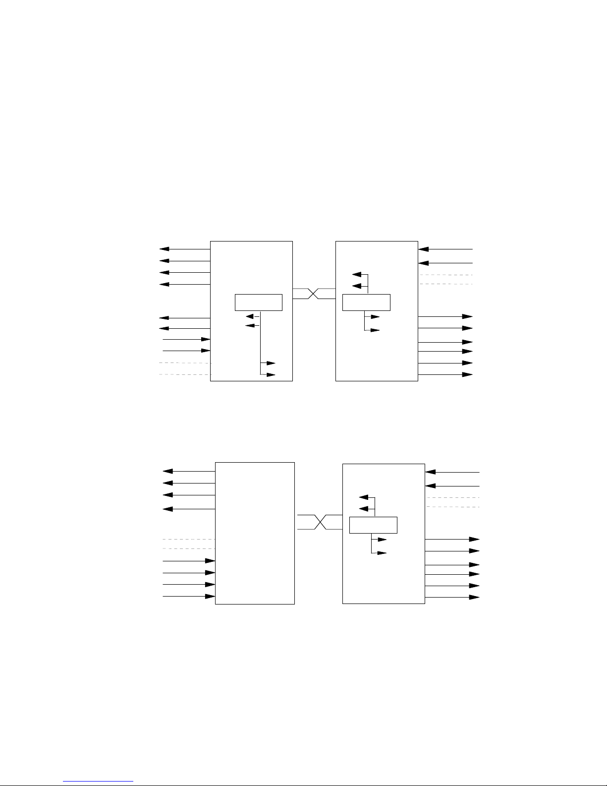
2.5.3 Internal Timing
Model F282X modems can supply clock frequencies internally while configured as an RS-530
DCE. SW3, Positions 4 through 8 allow the user to select 18 different clock frequencies, as listed in
Table 2. The internal timing mode is set by turning on SW4, Position 1. When SW4, Position 1 is in the
ON position, the board is configured as a null modem. In this configuration, the terminal timing (TT)
clock signals on input pins 11 and 24 of the DB25 interface and the transmit clock signals (TXC), input
on pins 12 and 15 of a DTE unit, are disconnected and replaced with the internally generated clock. In a
null modem configuration, the internal clock is used throughout the circuit. In the interface extender
configuration, the internal clock generated by the DCE modem is output on pins 11 and 24 of the DTE
modem (See Figure 5). When SW4, Position 1 is in the OFF position the internal clock is off.
RXD (A)
RXD (B)
RXC (A)
RXC (B)
TXC (A)
TXC (B)
TXD (A)
TXD (B)
TT (A)
TT (B)
16
17
15
12
14
24
11
DCE
3
9
OSC
2
F / O
DCE
OSC
OSC
15
12
16
17
14
24
11
9
2
3
TXD (A)
TXD (B)
TT (A)
TT (B)
TXC (A)
TXC (B)
RXD (A)
RXD (B)
RXC (A)
RXC (B)
INTERNAL TIMING -
NULL MODEM / MODEM LINK
TXD (A)
TXD (B)
TT (A)
TT (B)
TXC (A)
TXC (B)
RXD (A)
RXD (B)
RXC (A)
RXC (B)
14
24
11
15
12
16
17
DTE
2
F / O
3
9
INTERNAL TIMING -
INTERFACE EXTENDER
DCE
OSC
OSC
15
12
16
17
14
24
11
9
2
3
TXD (A)
TXD (B)
TT (A)
TT (B)
TXC (A)
TXC (B)
RXD (A)
RXD (B)
RXC (A)
RXC (B)
FIGURE 5. INTERNAL TIMING MODES
8
www.versitron.com
Page 13

2.6 LOOPBACK
The Model F282X has two loopback features. The first loopback feature allows the user to test the
fiber-optic circuitry of the unit, the fiber-optic circuitry of the unit at the receiving end, the copper
circuitry of the unit, and the copper circuitry of the unit at the receiving end. The second loopback
feature loops the control signals RTS and CTS.
2.6.1 Fiber / Copper Loopback
This loopback feature of the Model F282X allows the user to test the fiber-optic circuitry of the
unit and the fiber-optic circuitry of the unit at the receiving end. The fiber-optic input and outputs are
connected to a multiplexer. The multiplexer is controlled by the front-panel switch (SW1). When SW1
is ON, the multiplexer control bit goes high, the fiber-optic input data is looped to the fiber-optic output
and sent back to the source. The copper signal enters the board through the interface circuitry to the
multiplexer circuit. The signals get multiplexed, demultiplexed and transmitted back to their source.
This is true for all data, clock, and control signals. If the fiber-optic output and input signals match, and
the copper signals match, the optical and interface circuits of both units are working properly. When
SW1 is OFF, the multiplexer control bit goes low, and the unit functions normally.
2.6.2 Remote / Local Loopback
The Remote / Local Switch, SW4, Position 3, is used to loop control signals RTS and CTS. This
is to accommodate equipment that lacks the ability to respond to an RTS signal. When SW4, Position 3
is ON, a CTS input signal is connected to RTS output and an RTS input is connected to CTS output.
When SW4, Position 3 is OFF, CTS-IN is connected to CTS-OUT and RTS-OUT is connected to RTSIN. See Table 3.
2.7 INITIAL CHECKOUT PROCEDURE
The Model F282X FOM II Series products contain no power on/off switch. Once the unit is
properly installed and power is applied it may be considered fully operational. The power indicator
should remain on as long as power is supplied to the unit
Before beginning system operation the following items should be checked to verify proper
installation:
1. Verify that the power plug is seated fully into the modem or the modem is seated firmly in the rack mount enclosure.
2. Verify that the fiber-optic cable is crossed transmit to receive from unit one to unit two.
3. Verify that the alarm LED goes out when the signal is applied to the optical receiver of the F282X.
4. Verify the switch settings for the circuit configuration (i.e. internal/external timing).
If a malfunction is detected during the initial checkout procedure, refer to Chapter 5 for
information on isolating the malfunction in the unit.
9
www.versitron.com
Page 14

SECTION 3
OPERATION
3.1 INTRODUCTION
This chapter contains a description of the operating controls and indicators associated with the
Model F282X FOM II Series modems. Since the Model F282X is designed for continuous and
uninterrupted operation, there are no operating requirements. Once the Model F282X is powered up it
should remain in service as long as required.
3.2 STATUS INDICATORS/AUDIBLE ALARM
There are 7 indicators on the Model F282X: power (PWR), alarm (ALM), transmit data (TXD),
receive data (RXD), transmit clock (TXC), receive clock (RXC), and Loopback (LOOP). No audible
alarm is available.
3.3 OPERATING CONTROLS
The only operating controls associated with the Model F282X modems are those used to select
between DTE/DCE, internal/external clock selection, internal clock data rate, and the two loopback
functions. These selections are normally made only at the time of installation. Further changes are not
required unless the system requirements change.
10
www.versitron.com
Page 15

4.1 INTRODUCTION
Basic operation of the Model F282X is similar to a four-channel, full duplex multiplexer. The first
channel is used for data. The next two channels are used for transmit and receive clock, while the fourth
multiplexer channel is used for aggregated control signals. This technique provides full transparency for
the link, even when both clocks originate at the modem. The modem supplies both transmit and receive
clocks to the Model F282X, which are transmitted through the link and applied directly to the terminal.
The interface control signals are processed in a similar manner. The Request to Send signal from
the terminal is transmitted through the link and applied to the modem. When the modem responds with
Clear to Send, it will be transmitted through the link and applied to the terminal. With this technique,
the terminal will see the RTS/CTS delay established by the modem. The unit is also capable of looping
RTS/CTS for interface equipment that does not support control signals.
If a fully transparent synchronous link is not required, the clock and control paths may be used as
additional asynchronous data paths. The transmit and receive clock inputs will handle data rates from 0
to 76.8 Kbps asynchronously; the control paths will handle data rates up to 1 Kbps with 5% distortion.
SECTION 4
THEORY OF OPERATION
11
www.versitron.com
Page 16

5.1 INTRODUCTION
This chapter contains general information designed to isolate a malfunction in the Model F282X to
a replaceable unit. These units are not equipped with redundancy. Therefore, a failure in one of these
units would interrupt service.
5.2 FAULT ISOLATION
The steps in Table 4 should be taken to check a non-operating modem.
STATUS INDICATOR PROBABLE CAUSE CORRECTIVE ACTION
POWER (PWR) LED is off. No AC power. Check that both ends of the Transformer
Blown Fuse. Replace with 250V 1A slo-blo fuse.
Other power supply circuit
LOSS of OPTICAL POWER (LOP)
LED is on.
DATA and CLOCK (TXD, RXD, TXC,
RXC) LEDs are off or not responding as
expected.
No input on the electrical
DATA AND CLOCK signal inverted. Switches/Jumpers in wrong
DATA signal inverted. Inverted input on the electrical
SECTION 5
MAINTENANCE AND TROUBLESHOOTING
are connected.
Contact VERSITRON Customer Service
problem.
Incorrect optical signal level
received at receiver input.
Switches/Jumpers in wrong
position.
interface connector.
position.
interface connector.
for assistance.
1. Check that fiber-optic cable is properly
connected to RX connector.
2. Check that the remote unit power is on
and the TX fiber-optic connector is
connected properly.
3. Measure the optical levels on both ends
(if possible) in order to check the optical
link.
4. Contact VERSITRON Customer
Service for assistance.
Check that the switch/jumper is set for the
correct electrical interface.
Check that the interface connector is
connected securely.
Check that the switch/jumper is set for the
correct electrical interface.
Check that the interface connector is
wired per interface standard RS-530.
TABLE 4. NON-OPERATIONAL INDICATORS
12
www.versitron.com
 Loading...