

Page 1

Reference
Reference
ReferenceReference
Manual
Manual
ManualManual
VSBC-8
Pentium III/Celeron based SBC
with Ethernet, Video, Audio and
Industrial I/O
Page 2

Page 3

VSBC-8
Pentium III/Celeron based SBC
with Ethernet, Video, Audio and
Industrial I/O
MVSBC-8
Page 4

Page 5
Product Release Notes
This page includes recent changes or improvements that have been made to this
product. These changes may affect its operation or physical installation in your
application. Please read the following information.
Rev 3 Release
• Initial public release.
Rev 2 Release
• Beta release only.
Rev 1 Release
• Pre-production only. No customer releases.
Support Page
The VSBC-8 Support Page, at http://www.versalogic.com/private/vsbc8support.asp, contains
additional information and resources for this product including:
• Reference Manual (PDF format)
• Operating system information and software drivers
• Data sheets and manufacturers’ links for chips used in this product
• BIOS information and upgrades
• Utility routines and benchmark software
Note: This is a private page for VSBC-8 users only. It cannot be reached through our web site. You must
enter this address directly to find the support page.
Page 6

Page 7

Model VSBC-8
Pentium III/Celeron based SBC with Ethernet, Video, Audio
and Industrial I/O
REFERENCE MANUAL
Doc. Rev 06/06/2003
V
ERSALOGIC CORPORATION
WWW.VERSALOGIC.COM
Although every effort has been made to ensure this document is error-free, VersaLogic makes no
representations or warranties with respect to this product and specifically disclaims any implied
warranties of merchantability or fitness for any particular purpose.
VersaLogic reserves the right to revise this product and associated documentation at any time
without obligation to notify anyone of such changes.
PC/104 and the PC/104 logo are trademarks of the PC/104 Consortium.
3888 Stewart Road
Eugene, OR 97402
(541) 485-8575
Fax (541) 485-5712
Contents Copyright ©2003
All Rights Reserved
Notice:
Page 8

Page 9

Table of Contents
1. Introduction ...............................................................................................................1
Description.......................................................................................................................... 1
Technical Specifications..................................................................................................... 3
Technical Support...............................................................................................................4
Repair Service........................................................................................................ 4
2. Configuration / Operation .........................................................................................5
Overview............................................................................................................................. 5
Electrostatic Discharge.......................................................................................... 5
Lithium Battery...................................................................................................... 5
Mounting Support.................................................................................................. 5
Initial Configuration and Setup .......................................................................................... 6
Recommended Components .................................................................................. 6
DRAM Module...................................................................................................... 6
Cables / Peripheral Devices................................................................................... 6
CMOS Setup / Boot Procedure Preliminary....................................................................... 7
Operating System Installation ............................................................................................ 8
Windows 98 & newer versions.............................................................................. 8
QNX Neutrino ....................................................................................................... 8
Redhat Linux 7.X................................................................................................... 8
DOS ....................................................................................................................... 8
3. Reference...................................................................................................................9
Dimensions and Mounting.................................................................................................. 9
Hardware Assembly ............................................................................................ 10
Standoff Locations............................................................................................... 10
External Connectors ......................................................................................................... 11
Connector Location Diagram ..............................................................................11
Connector Functions and Interface Cables.......................................................... 12
Jumper Block Locations ................................................................................................... 13
Jumper Summary................................................................................................. 14
Power Supply....................................................................................................................16
Power Connectors................................................................................................ 16
Power Requirements............................................................................................ 17
Lithium Battery.................................................................................................... 17
CPU................................................................................................................................... 18
Processor Replacement........................................................................................ 18
Processor Side Bus Selection .............................................................................. 18
Processor Power Management............................................................................. 19
System RAM .................................................................................................................... 20
Compatible Memory Modules............................................................................. 20
CMOS RAM..................................................................................................................... 20
Clearing CMOS RAM ......................................................................................... 20
iii
Page 10

Table of Contents
Real Time Clock............................................................................................................... 20
Setting the Clock ................................................................................................. 20
Battery Backed Static RAM ............................................................................................. 20
Disk on Chip ..................................................................................................................... 21
Enable / Disable................................................................................................... 21
Compatible Devices............................................................................................. 21
Installing the DOC Chip ...................................................................................... 21
CMOS Setup........................................................................................................ 21
Serial Ports........................................................................................................................ 22
COM Port Configuration ..................................................................................... 22
COM3 / COM4 RS-485 Mode Line Driver Control ........................................... 22
Serial Port Connectors......................................................................................... 23
Parallel Port ...................................................................................................................... 23
EIDE Hard Drive / CD-ROM Interfaces .......................................................................... 25
Utility Connector .............................................................................................................. 26
Keyboard/Mouse Interface .................................................................................. 26
Programmable LED............................................................................................. 26
External Speaker.................................................................................................. 27
Push-Button Reset
................................................................................................ 27
Floppy Drive Interface...................................................................................................... 27
Video Interface .................................................................................................................28
Software Configuration .......................................................................................28
Video Resolutions................................................................................................ 28
Video Output Connector...................................................................................... 28
Flat Panel Display Connector.............................................................................. 29
Compatible Flat Panel Displays .......................................................................... 30
Ethernet Interface ............................................................................................................. 31
BIOS Configuration............................................................................................. 31
Status LED........................................................................................................... 31
Ethernet Connector .............................................................................................. 31
Audio ................................................................................................................................ 32
Software Configuration .......................................................................................32
External Connections........................................................................................... 32
Watchdog Timer ............................................................................................................... 33
Enabling the Watchdog ....................................................................................... 33
Refreshing the Watchdog ....................................................................................33
CPU Temperature Monitor............................................................................................... 33
Analog Input ..................................................................................................................... 34
Hardware Configuration ...................................................................................... 34
External Connections........................................................................................... 34
Calibration ........................................................................................................... 34
Analog Control Register...................................................................................... 35
Digital Control / Analog Status Register............................................................. 36
ADC Data High Register ..................................................................................... 37
ADC Data Low Register...................................................................................... 38
Two’s Complement Data Format (±5V and ±10V Only) ................................... 39
Binary Format (0 to +5V and 0 to +10V Only)................................................... 40
Analog Input Code Example ............................................................................... 40
iv
Page 11

Table of Contents
USB 1.1 Interface ............................................................................................................. 41
Opto 22 (Digital I/O) Interface......................................................................................... 42
External Connections........................................................................................... 42
Rack Power.......................................................................................................... 43
Signal Direction................................................................................................... 43
Digital I/O Data Ports.......................................................................................... 43
Auxiliary Timer/Counter Channels .................................................................................. 44
Jumper Configuration.......................................................................................... 44
External Connections........................................................................................... 44
Counter / Timer Registers ................................................................................... 44
Operation ............................................................................................................. 44
PC/104 Expansion Bus ..................................................................................................... 45
Arranging the Stack ............................................................................................. 45
I/O Configuration ................................................................................................ 45
Memory and I/O Map ....................................................................................................... 46
Memory Map ....................................................................................................... 46
I/O Map................................................................................................................ 46
Interrupt Configuration..................................................................................................... 47
Special Control Register................................................................................................... 48
Revision Indicator Register .............................................................................................. 49
Watchdog Timer Hold-Off Register................................................................................. 49
Map and Paging Control Register .................................................................................... 50
Appendix A — Other References ...............................................................................51
v
Page 12

Page 13

Description
The VSBC-8 is a feature-packed single board computer designed for OEM control projects
requiring fast processing, industrial I/O, flexible memory options, and designed-in reliability and
longevity (product lifespan). It's features include:
•
Socket 370 processors
• Intel Celeron 350 MHz (equivalent)
• Intel Celeron 566 MHz
• Intel Pentium III 850 MHz
• Up to 256 MB system RAM
• Intel 440BX chipset
• 32-pin DiskOnChip site
• 10/100 Ethernet interface
• AGP based video
• Flat Panel Display support
• PC/104-Plus expansion site
• Dual PCI based IDE controllers
• Dual USB 1.1 interfaces
• PCI based audio
• 4 COM + 1 LPT port
• CPU temperature sensor
Introduction
• Keyboard and PS/2 mouse port
• Industrial I/O
• Analog input option
• 16 channel Opto 22 compatible
• Three spare 16-bit counter/timers
•
Two RS232/422/485 selectable ports
• Watchdog timer
• Vcc sensing reset circuit
• EBX Compliant. 5.75” x 8.00” footprint
• UL and CE compliant
• Flash BIOS with OEM enhancements
• Latching I/O connectors
• Customizing available
• Low power fanless version
• 3 extra 8254-style timer/counters
1
This Socket 370 compliant single board computer will accept Intel Flip-Chip Pentium and Intel
Flip-Chip Celeron chips. Processing speeds up to 850 MHz are available. The board is
compatible with popular operating systems such as Windows, QNX, VxWorks, and Linux.
A full complement of standard I/O ports is included on the board. Additional I/O expansion is
available through the high speed PCI-based PC/104-Plus expansion site (which supports both
PC/104 and PC/104-Plus expansion modules).
System memory expansion is supported with a high-reliability latching 168-pin DIMM socket.
Low power 3.3V 168-pin DIMM modules up to 256 MB are available. SDRAM PC-100 modules
are accepted (see specifications on page 3).
VSBC-8 Reference Manual Introduction – 1
Page 14

Description
The VSBC-8 features high reliability design and construction including latching I/O connectors.
It also features a watchdog timer, voltage sensing reset circuits, and self-resetting fuse on the 5V
supply to the keyboard, mouse, USB 1.1 and Opto 22 I/O ports.
VSBC-8 boards are subjected to a 48-hour burn-in and 100% functional testing and are backed
by a limited two-year warranty.
US-based manufacturing, careful parts sourcing, and US-based technical support ensure the
highest possible quality, reliability, service, and product longevity for this exceptional SBC.
2 – Introduction VSBC-8 Reference Manual
Page 15

Technical Specifications
Specifications are typical at 25°C with 5.0V supply unless otherwise noted.
Board Size:
Storage Temperature:
Free Air Operating Temperature:
Power Requirements:
System Reset:
DRAM Interface:
Video Interface:
IDE Interface:
Floppy Disk Interface:
Ethernet Interface:
Audio Interface:
Analog Input:
COM1–2 Interface:
COM3–4 Interface:
LPT Interface:
Opto 22 / Digital Interface:
BIOS:
Bus Speed:
Compatibility:
Specifications are subject to change without notice.
5.75" x 8.00" x 1.75"; EBX Compliant
–40° C to 85° C
0° C to +50° C free air, no airflow
0° C to +60° C 100 FPM airflow
-40° C to +85° C, no airflow (Extended temp. version)
(with 32 MB SDRAM, keyboard, and mouse)
VSBC-8b 350 MHz (equivalent) Celeron CPU fanless 5V ± 5% @ 3.2 A (15.9 W) typ.
VSBC-8c 566 MHz Celeron CPU 5V ± 5% @ 4.0 A (20.1 W) typ.
VSBC-8d 850 MHz Pentium CPU 5V ± 5% @ 5.5 A (27.4 W) typ.
VSBC-8e 350 MHz (equivalent) Celeron CPU extended temperature 5V ± 5% @ 3.3 A (16.5 W) typ.
+3.3V or ±12V may be required by some expansion modules
Vcc sensing, resets below 4.70V typ.
Watchdog timeout
One 168-pin DIMM socket.
8 to 256 MB, 3.3 volt, parity or non-parity PC-100 SDRAM.
Based on C&T 69030 chip. 4 MB VRAM standard. Resolutions to 1600 x 1200.
Optional flat panel display interface. 3.3V and 5V flat panel display support
Two channels, 40-pin .1” connectors. Supports high speed IDE Type 4 and Ultra DMA drives.
Supports up to four IDE devices (hard drives, CD-ROM, etc.)
One 34-pin connector, supports two floppy drives
10/100 Ethernet based on Intel 82559ER chip. On-board RJ-45 Ethernet cable connector.
16-bit Sound Blaster Pro compatible. PCI-based.
Non-amplified Line Out and Line In supported
8-channel, 12-bit, single-ended, 6 microsecond, channel independent input ranges:
±5, ±10, 0 to +5V, 0 to +10V
Note: Analog input is available only on -r versions.
RS-232, 16C550 compatible, 1.5M baud max.
RS-232/422/485, 16C550 compatible, 1.5M baud max.
Bi-directional/EPP/ECP compatible
16 channel, full compliance, ±24 ma outputs
General Software embedded BIOS with OEM enhancements
Field upgradable with Flash BIOS Upgrade Utility
CPU Bus: 100MHz/66MHz
PC/104-Plus (PCI): 33MHz
PC/104: 8MHz
PC/104 – Full compliance
Embedded-PCI (PC/104-Plus) – Full compliance, 3.3V or 5V modules
EBX – Full compliance
Technical Specifications
VSBC-8 Reference Manual Introduction – 3
Page 16

Technical Support
Technical Support
If you have problems that this manual can’t help you solve, first visit the VSBC-8 Product
Support web page at http://www.versalogic.com/private/vsbc8support.asp. If you have further
questions, contact VersaLogic for technical support at (541)485-8575. You can also reach our
technical support engineers via e-mail at [email protected].
http://www.versalogic.com/private/vsbc8support.asp
EPAIR SERVICE
R
If your product requires service, you must obtain a Returned Material Authorization (RMA)
number by calling (541) 485-8575.
VSBC-8 Support Website
Please provide the following information:
• Your name, the name of your company, and your phone number
• The name of a technician or engineer who we can contact if we have questions
• Quantity of items being returned
• The model and serial number (bar code) of each item
• A description of the problem
• Steps you have taken to resolve or repeat the problem
• The return shipping address
Warrant
Non-warranty Repair All non-warranty repairs are subject to diagnosis and labor charges,
Note! Please mark the RMA number clearly on the outside of the box before
y Repair All parts and labor charges are covered, including return shipping
charges for UPS 3rd Day Select delivery to United States addresses.
parts charges, and return shipping fees. We will need to know what
shipping method you prefer for return back to your facility, and we
will need to secure a purchase order number for invoicing the repair.
returning. Failure to do so can delay the processing of your return.
4 – Introduction VSBC-8 Reference Manual
Page 17

Overview
LECTROSTATIC DISCHARGE
E
Warning! Electrostatic discharge (ESD) can damage boards, disk drives, and other
Configuration / Operation
components. The circuit board must be only be handled at an ESD workstation. If
an approved station is not available, some measure of protection can be provided
by wearing a grounded antistatic wrist strap. Keep all plastic away from the board,
and do not slide the board over any surface.
After removing the board from its protective wrapper, place the board on a
grounded, static-free surface, component side up. Use an anti-static foam pad if
available.
The board should also be protected during shipment or storage by keeping inside a
closed metallic anti-static envelope.
2
Note! The exterior coating on some metallic anti-static bags is sufficiently conductive to
cause excessive battery drain if the bag comes in contact with the bottom side of
the VSBC-8.
ITHIUM BATTERY
L
Warning! To prevent shorting, premature failure, or damage to the lithium battery, do not
place the board on a conductive surface such as metal, black conductive foam, or
the outside surface of a metalized ESD protective pouch. The lithium battery may
explode if mistreated. Do not recharge, disassemble, or dispose of in fire. Dispose
of used batteries promptly.
OUNTING SUPPORT
M
Warning! The single board computer must be supported at all eight mounting points to
prevent excessive flexing when expansion modules are mated and demated. Flex
damage caused by excessive force on an improperly mounted circuit board is not
covered under the product warranty. See page 9 for more details.
VSBC-8 Reference Manual Configuration / Operation – 5
Page 18

Initial Configuration and Setup
Initial Configuration and Setup
The following list describes the recommended components and gives an abbreviated outline for
setting up a typical development system.
ECOMMENDED COMPONENTS
R
• VSBC-8 Single Board Computer
• 168-pin DIMM SDRAM Memory Module PC-100
• ATX Power Supply
• SVGA Video Monitor
• Keyboard with PS2 connector
• 3.5" Floppy Disk Drive (optional)
• IDE Hard Drive (optional)
• IDE CD ROM Drive (optional)
DRAM M
ODULE
• Insert DRAM module into the DIMM socket. Latch into place.
ABLES
C
ERIPHERAL DEVICES
/ P
• Plug video adapter cable (p/n VL-CBL-1007) into socket J1 and attach video monitor.
• Plug keyboard adapter cable (p/n VL-CBL-1602) into socket J13 and attach keyboard.
• Plug floppy data cable (p/n VL-CBL-3403) into socket J17 and attach floppy drive.
Note! Floppy drive should be connected after the twist in the cable.
• Plug hard drive data cable (p/n VL-CBL-4001) into socket J18. Attach hard drive and
CD ROM drive to the connectors at the opposite end of the cable.
• Plug power supply into J9.
• Attach power supply cables to external drives.
• Jumper hard drive to operate as a master device.
6 – Configuration / Operation VSBC-8 Reference Manual
Page 19

CMOS Setup / Boot Procedure Preliminary
CMOS Setup / Boot Procedure Preliminary
• Turn power on.
• Press the DEL key the instant that video is displayed (during the memory test).
• Verify correct CMOS Setup information (see table below)
• Insert bootable floppy disk into floppy drive or allow the system to boot from the hard
drive.
Basic CMOS Configuration
+------------------------------------------------------------------------------+
| System Bios Setup - Basic CMOS Configuration |
| (C) 2000 General Software, Inc. All rights reserved |
+---------------------------+--------------------+-----------------------------+
| DRIVE ASSIGNMENT ORDER: | Date:>Jan 01, 1980 | Typematic Delay : 250 ms |
| Drive A: Floppy 0 | Time: 00 : 00 : 00 | Typematic Rate : 30 cps |
| Drive B: (None) | NumLock: Disabled | Seek at Boot : Floppy |
| Drive C: (None) +--------------------+ Show "Hit Del" : Enabled |
| Drive D: (None) | BOOT ORDER: | Config Box : Enabled |
| Drive E: (None) | Boot 1st: Drive A: | F1 Error Wait : Enabled |
| Drive F: (None) | Boot 2nd: (None) | Parity Checking : (Unused) |
| Drive G: (None) | Boot 3rd: (None) | Memory Test Tick : Enabled |
| Drive H: (None) | Boot 4th: (None) | Test Above 1 MB : Disabled |
| Drive I: (None) | Boot 5th: (None) | Debug Breakpoints: (Unused) |
| Drive J: (None) | Boot 6th: (None) | Splash Screen : Disabled |
| Drive K: (None) +--------------------+-----------------+-----------+
| Boot Method: Boot Sector | IDE DRIVE GEOMETRY: Sect Hds Cyls | Memory |
+---------------------------+ Ide 0: Not installed | Base: |
| FLOPPY DRIVE TYPES: | Ide 1: Not installed | 640KB |
| Floppy 0: 1.44 MB, 3.5" | Ide 2: Not installed | Ext: |
| Floppy 1: Not installed | Ide 3: Not installed | 15MB |
+---------------------------+--------------------------------------+-----------+
Custom Configuration
+------------------------------------------------------------------------------+
| System BIOS Setup - Custom Configuration |
| (C) 2000 General Software, Inc. All rights reserved |
+---------------------------------------+--------------------------------------+
| 64KB Memory Page E000:0h : None | COM1 (03F8) Enable/IRQ : IRQ4 |
| CPU Temperature Threshold : 70 C | COM2 (02F8) Enable/IRQ : IRQ3 |
| Display Type : CRT | COM3 (03E8) Enable/IRQ : IRQ4 |
| Interrupt Vector Restore : Disabled | COM4 (02E8) Enable/IRQ : IRQ3 |
| Parallel Port Mode : SPP | LPT1 (0378) Enable/IRQ : IRQ7 |
| Reserved : (Unused) | PCI INT A : IRQ11 |
| I/O Register Base Address : 0E0h | PCI INT B : IRQ11 |
| Processor Throttling : Varies | PCI INT C : IRQ11 |
| Throttling Percentage : Varies | PCI INT D : IRQ11 |
| IDE 0 PIO Mode : Auto | IDE 2 PIO Mode : Auto |
| IDE 1 PIO Mode : Auto | IDE 3 PIO Mode : Auto |
+---------------------------------------+--------------------------------------+
Shadow Configuration
+------------------------------------------------------------------------------+
| System BIOS Setup - Shadow/Cache Configuration |
| (C) 2000 General Software, Inc. All rights reserved |
+---------------------------------------+--------------------------------------+
| Shadowing : >Chipset | Shadow 16KB ROM at C000 : Enabled |
| Shadow 16KB ROM at C400 : Enabled | Shadow 16KB ROM at C800 : Disabled |
| Shadow 16KB ROM at CC00 : Disabled | Shadow 16KB ROM at D000 : Disabled |
| Shadow 16KB ROM at D400 : Disabled | Shadow 16KB ROM at D800 : Disabled |
| Shadow 16KB ROM at DC00 : Disabled | Shadow 16KB ROM at E000 : Disabled |
| Shadow 16KB ROM at E400 : Disabled | Shadow 16KB ROM at E800 : Disabled |
| Shadow 16KB ROM at EC00 : Disabled | Shadow 64KB ROM at F000 : Enabled |
+---------------------------------------+--------------------------------------+
Note! Due to changes and improvements in the system BIOS, the information on your monitor
may differ from that shown above
.
VSBC-8 Reference Manual Configuration / Operation – 7
Page 20

Operating System Installation
Operating System Installation
The standard “PC” architecture used on the VSBC-8 makes the installation and use of most of
the standard x86 processor based operating systems very straight forward. The operating systems
listed below use the standard installation procedures as provided by the maker of the OS. If
special optimized hardware drivers are available for a particular operating system, you can find
these drivers, or a link to the drivers, at the VSBC-8 Product Support web page at
http://www.versalogic.com/private/vsbc8support.asp.
INDOWS
W
NEWER VERSIONS
98 &
Use the standard installation procedures
QNX N
EUTRINO
Use the standard installation procedure to install over a Windows 98 installation.
R
EDHAT LINUX
7.X
Use the standard installation procedures.
DOS
Use the standard installation procedures.
8 – Configuration / Operation VSBC-8 Reference Manual
Page 21
Dimensions and Mounting
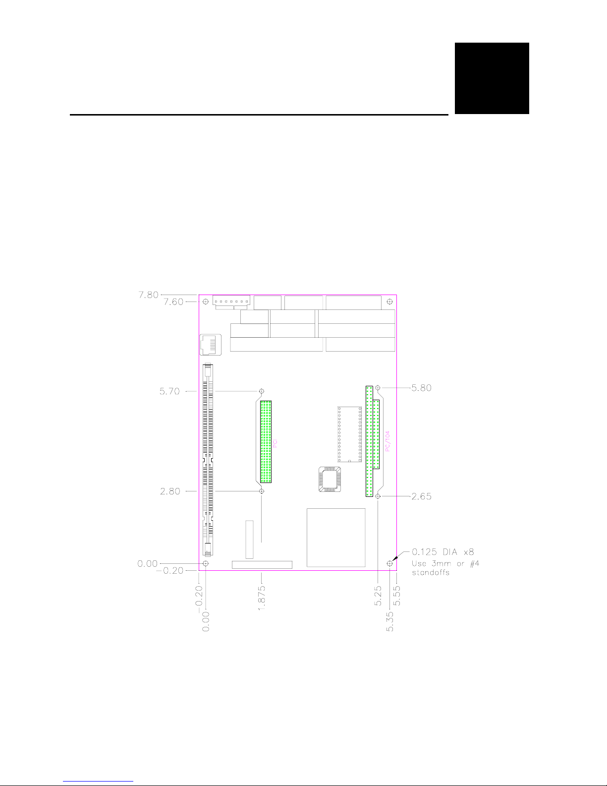
The VSBC-8 complies with all EBX standards which provide for specific mounting hole and
PC/104-Plus stack locations as shown in the diagram below.
Caution The single board computer must be supported at all eight mounting points to
prevent excessive flexing when expansion modules are mated and demated. Flex
damage caused by excessive force on an improperly mounted circuit board is not
covered under the product warranty.
Reference
3
VSBC-8 Reference Manual Reference – 9
Figure 1. Dimensions and Mounting Holes
(Not to scale. All dimensions in inches.)
Page 22
Dimensions and Mounting
ARDWARE ASSEMBLY
H
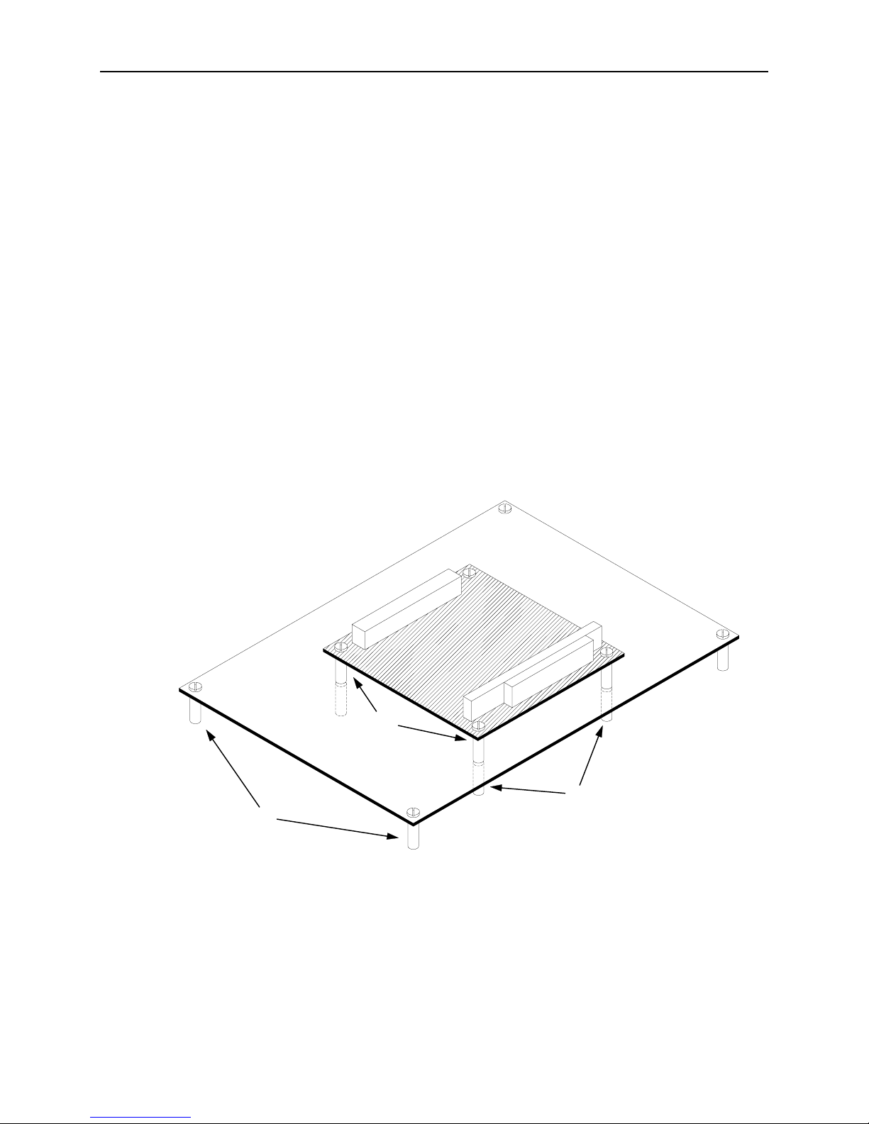
The VSBC mounts on four hardware standoffs using the corner mounting holes (A). These
standoffs are secured to the underside of the circuit board using pan head screws.
Four additional standoffs (B) must be used under the circuit board to prevent excessive flexing
when expansion modules are mated and demated. These are secured with four male-female
standoffs (C) threaded from the topside which also serve as mounting struts for the PC/104 stack.
The entire assembly can sit on a table top or it can be secured to a base plate. When bolting the
unit down, make sure to secure all eight standoffs (A and B) to the mounting surface to prevent
circuit board flexing. Refer to the drawing on page 9 for dimensional details.
An extractor tool is available (part number VL-HDW-201) to separate the PC/104 modules from
the stack.
Note! Standoffs and screws are available as part number VL-HDW-101.
TANDOFF LOCATIONS
S
A
10 – Reference VSBC-8 Reference Manual
C
B
Figure 2. Standoff Locations
Page 23
External Connectors
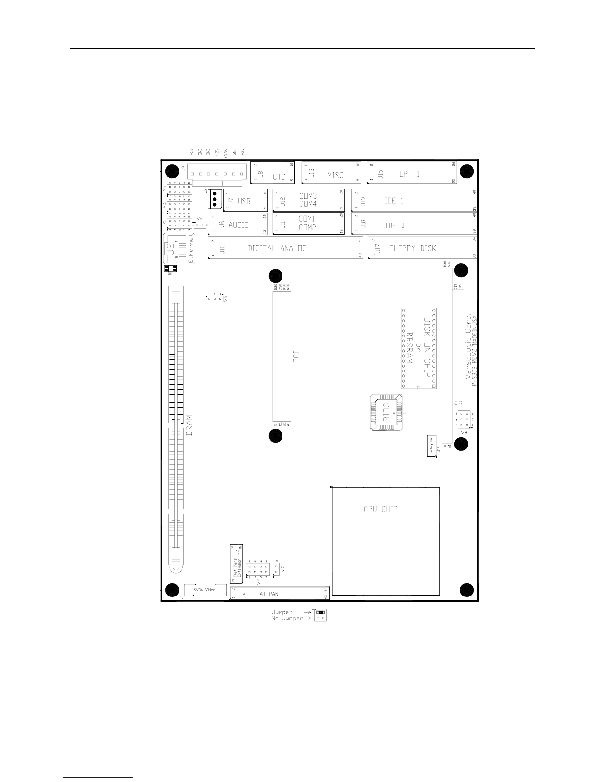
ONNECTOR LOCATION DIAGRAM
C
External Connectors
VSBC-8 Reference Manual Reference – 11
Figure 3. Connector Location Diagram
Page 24
External Connectors
ONNECTOR FUNCTIONS AND INTERFACE CABLES
C
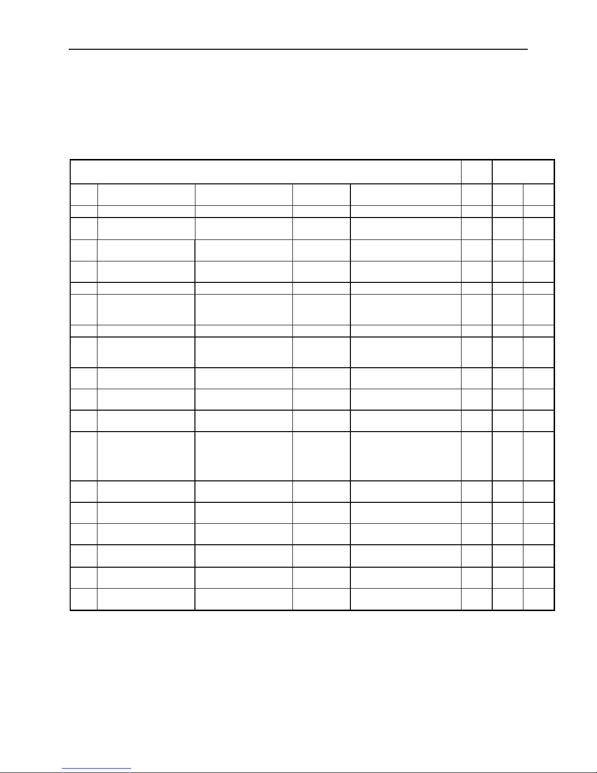
The table below notes the function of each connector, as well as mating connectors and cables,
and the page where a detailed pinout or further information is available.
Table 1: Connector Functions and Interface Cables
Connector Function
J1 SVGA Video Output 2mm 10-pin VersaLogic
J2 Ethernet RJ-45 Crimp-on Plug — — 31 N/A N/A
J3 PC/104-Plus Auxiliary
Power (–5V & –12V)
J4 Flat Panel Interface Adam Tech 2FCS-44-SG +
J5 Flat Panel Interface Adam Tech 2FCS-16-SG +
J6 Audio 3M 3452-7600 32 .875 6.600
J7* Dual USB 1.1 Connector Molex 14-56-2051 VersaLogic
J8 Counter / Timer Signals 3M 3473-7600 User supplied 44 1.625 7.525
Main Power Input
J9
(EBX Compliant)
J10* Opto-22 Interface and
Analog Input (-r version)
J11* COM1 and COM2 Ports 3M 3421-7600 VersaLogic
J12* COM3 and COM4 Ports 3M 3421-7600 VersaLogic
Speaker, IDE LED,
J13*
Programmable LED, Fused
Vcc, Keyboard, PS/2
mouse, Push-Button Reset
J14 Fan Power Output (+5V) Molex 22-01-3027 or
J15* LPT1 Port 3M 3399-7600 VersaLogic
J16 PLD Reprogramming Port
(Factory use Only)
J17* Floppy Drive Interface 3M 3414-7600 VersaLogic
J18* IDE Hard Drive Channel 0 3M 3417-7600 VersaLogic
J19* IDE Hard Drive Channel 1 3M 3417-7600 VersaLogic
Molex 10-11-2033 +
Molex 08-50-0005 (3ea.)
Adam Tech 2CTA §
Adam Tech 2CTA §
Molex 09-50-8073 +
Molex 08-52-0072 (7 ea.)
3M 3425-7600 VersaLogic
3M 3452-7600 VersaLogic
Molex 22-01-2025
— — — — 4.750 2.490
Mating
Connector
Transition
Cable
VL-CBL-1007
See connectorJ9See connector J9 16 .745 6.980
Custom Contact Factory 29 1.125 -.100
Custom Contact Factory 29 1.205 .195
VL-CBL-0501
(two required)
VersaLogic
VL-CBL-2021
VL-CBL-5007
VL-CBL-2001
VL-CBL-2001
VL-CBL-1602
Provided with
fan assembly
VL-CBL-2601
VL-CBL-3403
VL-CBL-4001
VL-CBL-4001
1 foot 10-pin socket to 15-pin
D-sub SVGA connector
6 inch transition cable. 5 pin
connector to USB receptacle
connector.
Interface from industry
standard ATX power supply (to
J3 and J9)
1.5 foot, 50-pin socket to 34pin socket and 16-pin socket
1 foot, 20-pin socket to two
DB9F serial port connectors
1 foot, 20-pin socket to two
DB9F serial port connectors
1 foot breakout cable. 16-pin
socket to two 6-PIN mini DIN
panel mount, programmable
LED and HD activity LED,
speaker, and reset switch.
— 5.095 .380
1 foot 26-pin socket to DB-25F
connector
1.5 foot 34-pin dual floppy drive
interface cable
1.5 foot 40-pin dual IDE drive
interface cable
1.5 foot 40-pin dual IDE drive
interface cable
Cable
Description Page
28 .445 -.100
41 1.125 7.025
16 .375 7.550
42, 34 .825 6.175
23 2.025 6.600
23 2.025 7.025
26 2.525 7.525
23 3.725 7.525
27 3.725 6.175
25 3.425 6.600
25 3.425 7.025
Pin 1 Location
‡
X Coord. Y Coord.
*
Note: These standard .100" dual-row low profile headers are 3M 2500 series compatible. They are compatible with 3M
snap-in latches, socket retaining clips, polarizing posts, and keys.
Note: This connector is a 2.00mm housing and crimp terminal style. Number of crimp terminals depends upon flat panel
§
display model being used.
Note: Relative to lower left hand mounting hole. See page 9, Figure 1.
‡
12 – Reference VSBC-8 Reference Manual
Page 25
Jumper Block Locations
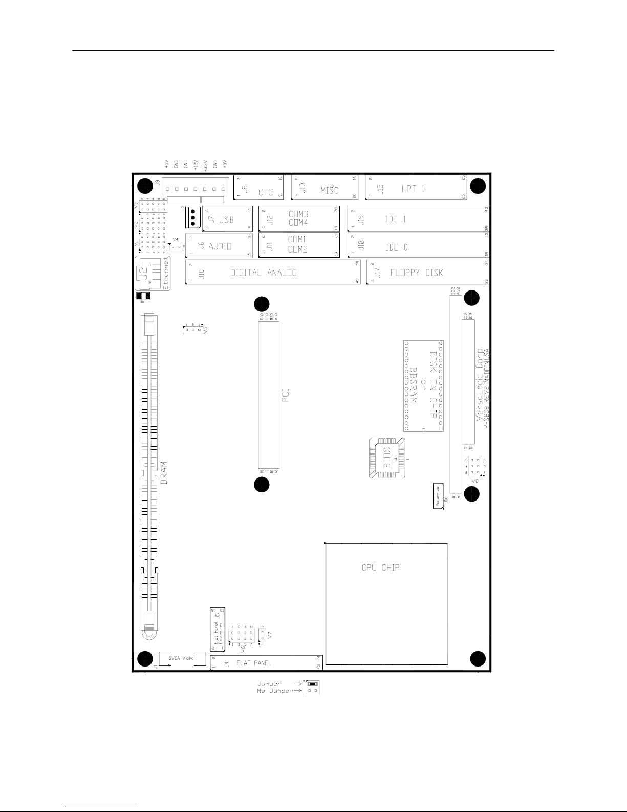
Note! Jumpers shown in as-shipped configuration.
Jumper Block Locations
VSBC-8 Reference Manual Reference – 13
Figure 4. Jumper Block Location
Page 26
Jumper Block Locations
UMPER SUMMARY
J
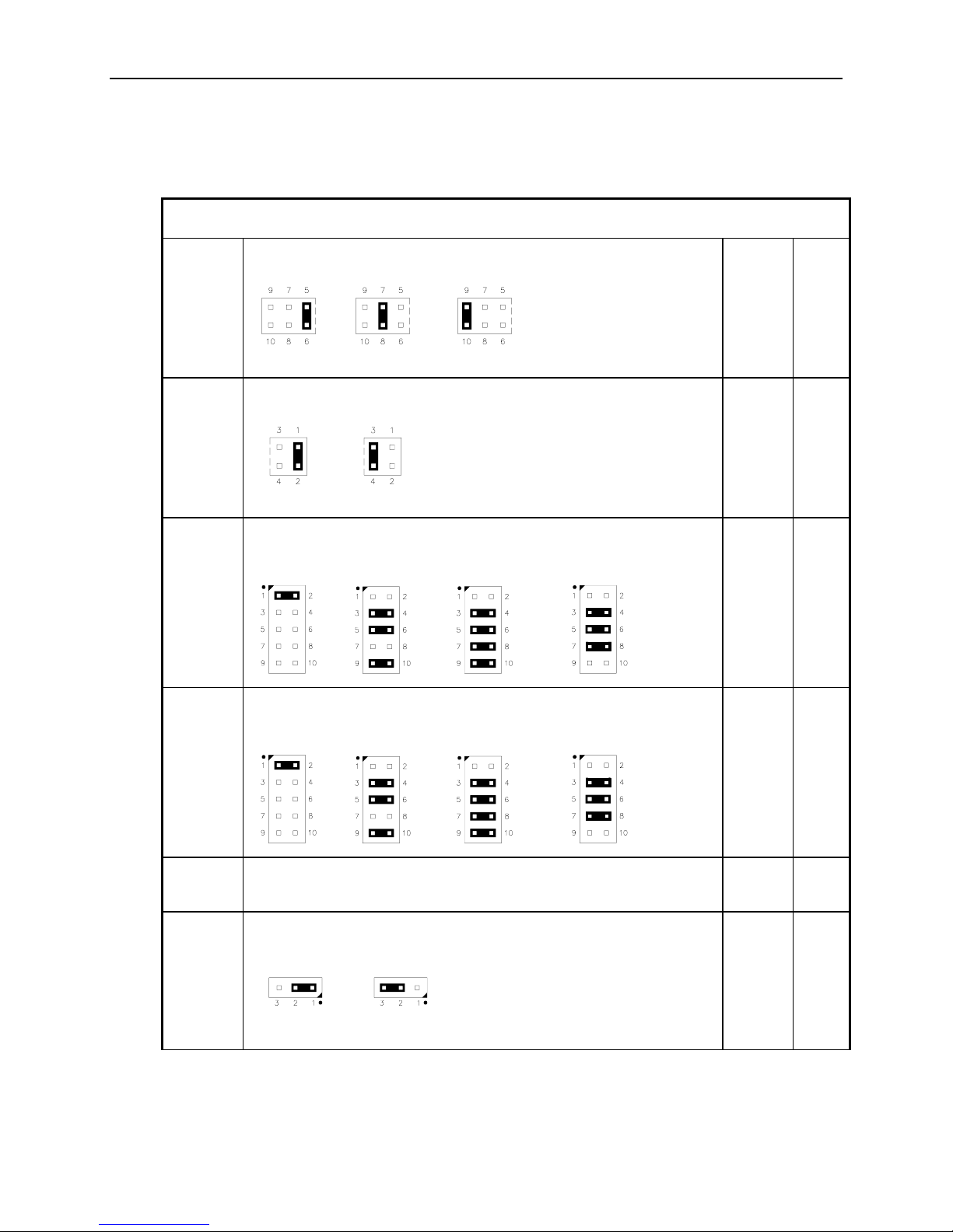
Table 2: Jumper Summary
Jumper
Block Description
V1
V1
V2
Counter/Timer 5 Clock Source
6 MHz CTC#4 External Input
Note! Only ½ of jumper block V1 is shown in this picture.
Counter/Timer 4 Clock Source
External Input 6 MHz
Note! Only ½ of jumper block V1 is shown in this picture.
COM4 Configuration
RS-485 RS-485
RS-232 RS-422 Endpoint Station Intermediate Station
As
Shipped Page
6 MHz 44
6 MHz 44
RS-232 22
V3
V4
V5
COM3 Configuration
RS-485 RS-485
RS-232 RS-422 Endpoint Station Intermediate Station
Opto 22 I/O Rack Power
In — I/O rack power provided by VSBC
Out — I/O rack power provided externally
CMOS RAM and Real Time Clock Erase
Normal
Erase Operation
Note! Do not operate the board with the jumper in the erase position. Leave the
jumper in position V5[1-2] for at least one full minute to fully erase CMOS RAM.
RS-232 22
In 42
Normal 20
14 – Reference VSBC-8 Reference Manual
Page 27
umper Summary Pg 2
Jumper
Block Description
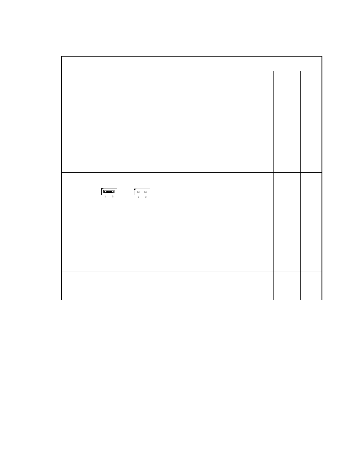
V6
Flat Panel Selection
V6[7-8] V6[5-6] V6[3-4] V6[1-2] Number Type
In In In In — —
In In In Out 1
In In Out In 2
In In Out Out 3
In Out In In 4
In Out In Out 5
In Out Out In 6
In Out Out Out 7
Out In In In 8
Out In In Out 9
Out In Out In 10
Out In Out Out 11
Out Out In In 12
Out Out In Out 13
Out Out Out In 14
Out Out Out Out 15
V7
Processor Side Bus Speed
66 MHz Selected by Processor
Jumper Block Locations
As
Shipped Page
29
1024x768 Dual Scan STN Color
128x1024 TFT Color
640x480 Dual Scan STN Color
800x600 Dual Scan STN Color
640x480 Sharp TFT Color
640x480 18-bit TFT Color
1024x768 TFT Color
800x600 TFT Color
800x600 TFT Color
800x600 TFT Color
800x600 Dual Scan STN Color
800x600 Dual Scan STN Color
1024x768 TFT Color
1280x1024 Dual Scan STN Color
1024x600 Dual Scan STN Color
out 18
V8[1-2]
V8[3-4]
V8[5-6]
System BIOS Selector
In — Primary System BIOS occupies F0000h to FFFFFh
Out — Secondary System BIOS occupies F0000h to FFFFFh
Note! The secondary System BIOS is field upgradable using the BIOS upgrade
utility. See www.versalogic.com/private/vsbc8support.asp
for further information.
Video BIOS Selector
In — Primary Video BIOS occupies C0000h to CFFFFh
Out — Secondary Video BIOS occupies C0000h to CFFFFh
Note! The secondary Video BIOS is field upgradable using the BIOS upgrade
utility. See www.versalogic.com/private/vsbc8support.asp
for further information
General Purpose Input 1
In — CPU reads bit as 1
Out — CPU reads bit as 0
Note! This jumper is reserved. Contact factory for more information.
In —
In —
In —
VSBC-8 Reference Manual Reference – 15
Page 28
Power Supply
Power Supply
OWER CONNECTORS
P
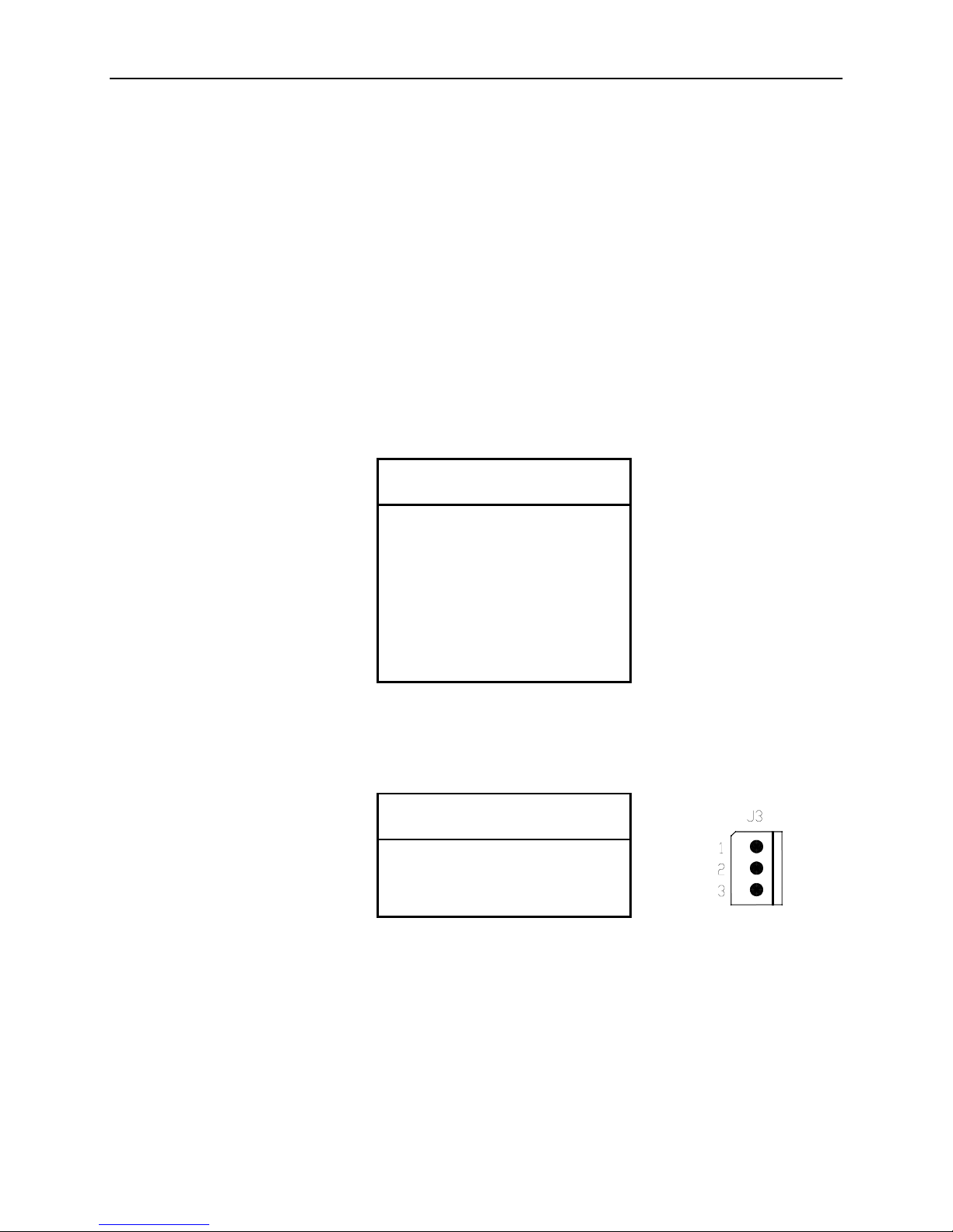
Main power is applied to the VSBC-8 through an EBX style 7-pin polarized connector (mating
connector Molex Housing 09-50-8073, Pins 08-52-0072). A 3-pin auxiliary power input
connector is also provided to supply –5V and –12V to the PC/104-Plus stack.
See page 11 for connector pinout and location information.
Warning! To prevent severe and possibly irreparable damage to the system, it is critical that
the power connectors be wired correctly. Make sure to use both +5VDC pins and
all three ground pins to prevent excess voltage drop.
Table 3: Main Power Connector Pinout
J9
Signal
Pin
Name Description
1 +5VDC Power Input
2 Ground Digital Ground
3 Ground Digital Ground
4 +12VDC Power Input
5 +3.3VDC Power Input
6 Ground Digital Ground
7 +5VDC Power Input
Note! The +3.3VDC and +12VDC inputs on the main power connector are only required
for PC/104-Plus expansion modules that require these voltages.
Table 4: Auxiliary Power Connector Pinout
J3
Signal
Pin
Name Description
1 –5VDC Power Input
2 Ground Digital Ground
3 –12VDC Power Input
Note! The Auxiliary Power Connector uses VersaLogics CBL-2021 Power Adapter
Cable. Auxiliary voltages are only required for PC/104-Plus expansion modules
that require these voltage.
16 – Reference VSBC-8 Reference Manual
Page 29

Power Supply
OWER REQUIREMENTS
P
The VSBC-8 requires only +5 volts (±5%) for proper operation. The voltage required for the RS232 ports and analog input sections are generated with a DC/DC converter. A variable lowvoltage supply circuit provides power to the CPU and other on-board devices.
The exact power requirement of the VSBC-8 depends on several factors, including memory
configuration, CPU speed, peripheral connections, type and number of expansion modules, and
attached devices. For example, PS/2 keyboards typically draw their power directly from the
VSBC-8, and driving long RS-232 lines at high speed can increase power demand.
ITHIUM BATTERY
L
Warning! To prevent shorting, premature failure, or damage to the lithium battery, do not
place the board on a conductive surface such as metal, black conductive foam, or
the outside surface of a metalized ESD protective pouch. The lithium battery may
explode if mistreated. Do not recharge, disassemble, or dispose of in fire. Dispose
of used batteries promptly.
Normal battery voltage should be at least 3.0V. If the voltage drops below 3.0V, contact the
factory for a replacement (part number T-HB
3/5-3). Life expectancy under normal use is
approximately 10 years.
Note! The VSBC-8 is designed to boot even with a dead or removed battery. See page 20
for further information.
VSBC-8 Reference Manual Reference – 17
Page 30

CPU
CPU
ROCESSOR REPLACEMENT
P
Removal or replacement of CPU is not recommended, doing so may damage the CPU. These
flip-chip style 370-pin CPUs have the chip dies mounted an a thin substrate. If the substrate is
flexed too far, damage will occur to the die bonds. Such damage will not be covered under the
board warranty.
ROCESSOR SIDE BUS SELECTION
P
Pentium and Celeron CPU’s normally select their own Processor Side Bus Speed. A jumper
installed in V7 will override the CPU and will force a 66 MHz speed.
18 – Reference VSBC-8 Reference Manual
Page 31
CPU
ROCESSOR POWER MANAGEMENT
P
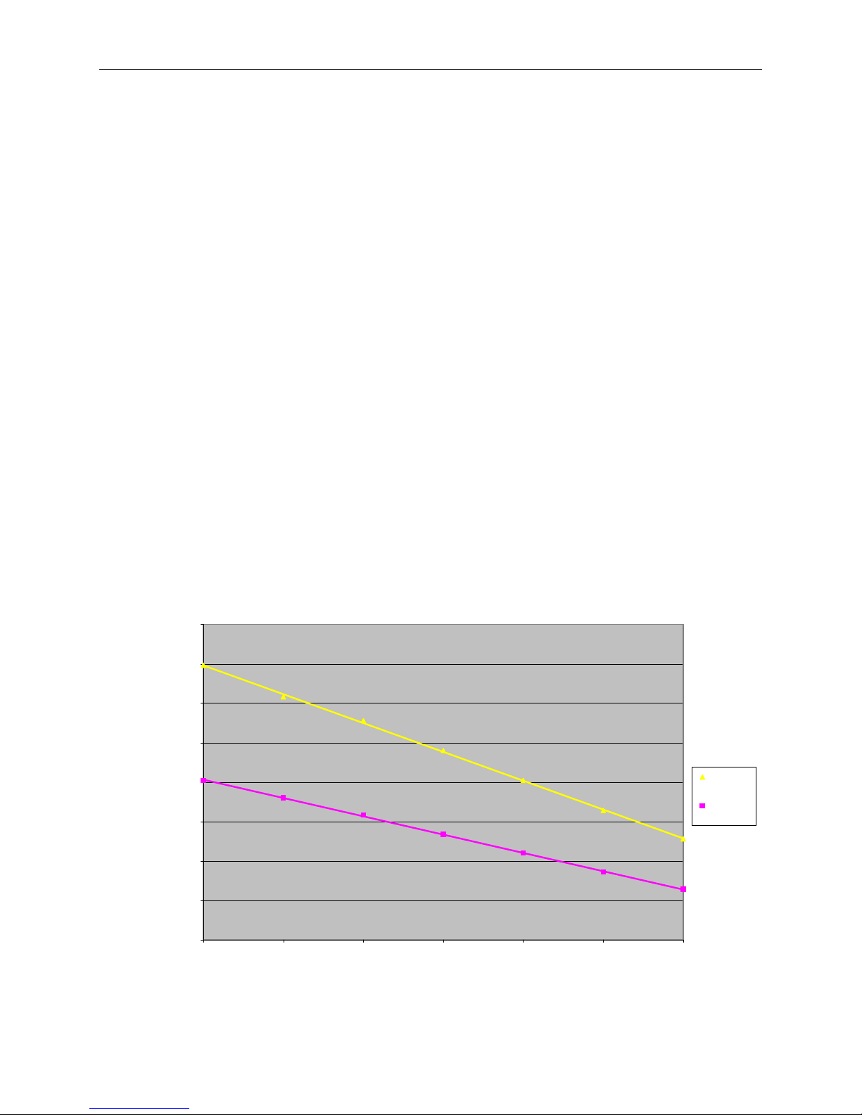
A form of power management called "throttling" is supported on the VSBC-8. This is an Intel
440BX chipset feature that has been augmented with an I/O control bit in the VersaLogic Special
Control Register. CMOS Setup options have been implemented to select throttling percentages
from 12.5% to 75%, and to enable or disable throttling. Throttling works by activating the CPU
Stop-Clock line every 250 microseconds to create a duty-cycle relative to the selected throttling
percentage. These throttling percentages refer to the relative time the CPU is in a stopped mode.
If throttling is enabled with the percentage set to 75%, the CPU will run at full speed (566 MHz
for the VSBC-8b, VSBC-8c or VSBC-8e and 850MHz for the VSBC-8d) for 62.5 microseconds
(25%) and will be off for 187.5 microseconds (75%) every 250 microsecond period.
Once the throttling percentage is initialized in the CMOS Setup, it can be enabled and disabled
by writing to the “Throttle” control bit in the VersaLogic Special Control Register. See page 48.
This gives the user a very simple means to throttle back during a time of little activity, and to reestablish full power when needed.
The VSBC-8b Low Power Fanless and the VSBC-8e versions are 566 MHz Celerons with
throttling always enabled at a minimum of 37.5% (which gives an effective CPU speed of 350
MHz). It can be slowed down to the maximum throttling rate of 75%, but not less than 37.5%.
The Throttle control bit in the VersaLogic Special Control Register can not be changed on the
VSBC-8b and VSBC-8e. Contact the factory for information on how to change the throttling
percentage via indexed PCI based registers in the chipset.
Typical Power vs Throttling
30
27.5
25
22.5
20
17.5
Typical Power (Watts)
15
12.5
10
0.0% 12.5% 25.0% 37.5% 50.0% 62.5% 75.0%
Throttling
Table 5: Power vs Throttling
850 MHz
Pentium III
566 MHz
Celeron
VSBC-8 Reference Manual Reference – 19
Page 32

System RAM
System RAM
OMPATIBLE MEMORY MODULES
C
The VSBC-8 will accept one 168-pin DIMM memory module with the following characteristics:
• Size 8 to 256 MB
• Voltage 3.3 Volt
• Error Detection Parity or Non-Parity
• Error Correction ECC or Non-ECC
• Type SDRAM, PC-100
Note: Parity and ECC features are not supported in the BIOS.
CMOS RAM
LEARING
C
Jumper V5[2-3] is normally inserted to provide battery power to the CMOS RAM circuits. The
jumper can be briefly moved to position V5[1-2] to erase the contents of the CMOS RAM should
it become necessary to do so. Do not operate the board with the jumper in the erase position.
Note! The jumper should remain in position V5[1-2] for a full minute to properly erase
CMOS RAM
the CMOS RAM contents.
Real Time Clock
The VSBC features a year 2000 compliant, battery-backed 146818 compatible real time
clock/calendar chip. Under normal battery conditions, the clock will maintain accurate
timekeeping functions during periods when the board is powered off.
ETTING THE CLOCK
S
The CMOS Setup utility (accessed by pressing the [DEL] key during a system boot) can be used
to set the time/date of the real time clock.
Battery Backed Static RAM
A 32-pin socket (U20 on the I/O module) will accept a battery-backed static RAM chip for nonvolatile storage. We recommend using the Dallas 128Kx8 DS1645 series or the 512Kx8
DS1650/DS1250 memory devices. They need to be a 32-pin, 0.6" DIP, 200nS or faster part. The
BBSRAM is enabled in CMOS Setup.
20 – Reference VSBC-8 Reference Manual
Page 33
Disk on Chip
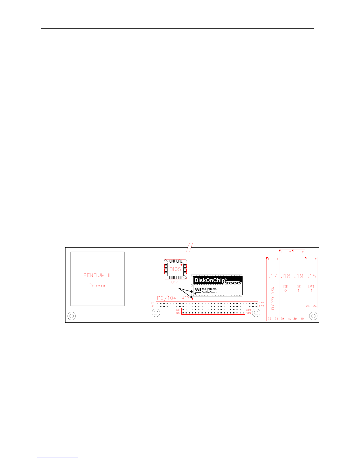
Socket U20 will accept an M-Systems DiskOnChip (DOC) Flash Disk for non-volatile,
read/write data storage. The DOC can be configured as a boot device
Disk on Chip
NABLE
E
/ D
ISABLE
The DOC can be enabled or disabled through CMOS Setup by going into the Custom screen and
setting "64 KB memory page E000:0h" “DiskOnChip” or "Disabled". When enabled, the DOC
appears in the upper memory region as an 64 K page frame from E0000h to EFFFFh.
OMPATIBLE DEVICES
C
Any 5 Volt, M-Systems series rev 1.10 or later 2000 DOC device will work.
I
NSTALLING THE
DOC C
HIP
1. Align pin 1 on the DOC with pin 1 of socket U20.
2. Push the DOC into the socket carefully until it is fully seated.
Warning! The DOC can be permanently damaged if installed incorrectly! When installing
or removing the DOC, be sure to align the chip as shown in the picture below. To
prevent electrostatic damage, first touch a grounded surface to discharge any static
electricity from your body.
CMOS S
ETUP
To enable the DOC as drive C on a system without a hard disk, set the CMOS setup of drive C to
“not installed”, and reboot the computer.
Note! The DOC needs to be formatted with the System files in order for it to be a
bootable drive. Refer to the M-Systems web site (www.m-sys.com) for
documentation on the DOC and details on making it a bootable device.
VSBC-8 Reference Manual Reference – 21
Pin #1
Figure 5. Disk On Chip Orientation
Page 34

Serial Ports
Serial Ports
The VSBC-8 features four on-board 16550 based serial channels located at standard PC I/O
addresses. COM1 and COM2 are RS-232 (115.2K baud) serial ports. IRQ lines are chosen in
CMOS Setup, and can be mapped to any IRQ line.
COM3 and COM4 can be operated in RS-232, RS-422, or RS-485 modes. Additional nonstandard baud rates are also available (programmable in the normal baud registers) of up to
1.5M. baud. IRQ lines are chosen in CMOS Setup, and can be mapped to any IRQ line.
Each COM port can be independently enabled or disabled in the CMOS Setup screen.
COM P
ORT CONFIGURATION
There are no configuration jumpers for COM1 and COM2 since they only operate in RS-232
mode.
Jumper V3 is used to configure COM3 for RS-232/422/485 operation. Jumper V2 is used to
configure COM4. See page 14 for jumper configuration details.
COM3 / COM4 RS-485 M
ODE LINE DRIVER CONTROL
The TxD+/TxD– differential line driver can be turned on and off by manipulating the DTR
handshaking line.
The following code example shows how to turn the line driver for COM3 or COM4 on and off:
mov dx,03ECh ; Point to COM3 Modem Control register
mov dx,02ECh ; or COM4 if desired
in al,dx ; Fetch existing value
or al,01h ; Set bit D0
out dx,al ; Turn DTR on (enables line driver)
in al,dx ; Fetch existing value
and al,0FEh ; Clear bit D0
out dx,al ; Turn DTR off (disables line driver)
22 – Reference VSBC-8 Reference Manual
Page 35
Note 1: Do not connect to these pins in RS-485 mode.
ERIAL PORT CONNECTORS
S
See the Connector Location Diagram on pages 11 and 12 for connector and cable information.
The pinout of the DB9 connector applies to use of the VersaLogic transition cable #VL-CBL-
2001.
Table 6: Connectors J11/J12 — Serial Port Pinout
COM1
COM2
J11
Pin
1 11 1 11 DCD — — 1
2 12 2 12 DSR — — 6
3 13 3 13 RXD* TxD+ (note 1) 2
4 14 4 14 RTS TxD– (note 1) 7
5 15 5 15 TXD* — — 3
6 16 6 16 CTS Ground Ground 8
7 17 7 17 DTR RxD– TxD/RxD– 4
8 18 8 18 RI RxD+ TxD/RxD+ 9
9 19 9 19 Ground Ground Ground 5
10 20 10 20 N/C — — —
J11
Pin
COM3
J12
Pin
COM4
J12
Pin
RS-232 RS-422 RS-485
Note 1: Do not connect to these pins in RS-485 mode.
DB9
Pin
VSBC-8 Reference Manual Reference – 23
Page 36

Parallel Port
Parallel Port
The VSBC-8 includes a standard bi-directional/EPP/ECP compatible LPT port which resides at
the PC standard address of 378h. The port can be enabled/disabled and interrupt assignments can
be made via the CMOS Setup screen. The LPT model is also set via the CMOS setup screen. The
pinout of the DB25 connector applies to use of the VersaLogic transition cable #VL-CBL-2601.
Table 7: LPT1 Parallel Port Pinout
J15
Centronics
Pin
Signal
1 Strobe Out 1
2 Auto feed Out 14
3 Data bit 1 In/Out 2
4 Printer error In 15
5 Data bit 2 In/Out 3
6 Reset Out 16
7 Data bit 3 In/Out 4
8 Select input Out 17
9 Data bit 4 In/Out 5
10 Ground — 18
11 Data bit 5 In/Out 6
12 Ground — 19
13 Data bit 6 In/Out 7
14 Ground — 20
15 Data bit 7 In/Out 8
16 Ground — 21
17 Data bit 8 In/Out 9
18 Ground — 22
19 Acknowledge In 10
20 Ground — 23
21 Port Busy In 11
22 Ground — 24
23 Paper End In 12
24 Ground — 25
25 Select In 13
26 No Connect — —
Signal
Direction
DB25
Pin
24 – Reference VSBC-8 Reference Manual
Page 37

EIDE Hard Drive / CD-ROM Interfaces
Two EIDE interfaces are available to connect up to four hard disk or CD-ROM drives.
Connector J18 is the primary IDE controller with a 40-pin .1” connector and connector J19 is the
secondary IDE controller with a 40-pin .1” connector. Use CMOS Setup to specify the drive
parameters of the attached drives.
Some older IDE drives, such as those that are PIO Mode 0-1, do not operate reliably with this
product. VersaLogic recommends the use of only PIO Mode 2-3 and Ultra DMA type drives
with this product.
Warning! Cable length must be 18" or less to maintain proper signal integrity. The grounds
in this connector should not be used to carry motor current.
Table 8: EIDE Hard Drive Connector Pinout
J18, J19
Pin
1 HRST* Host Reset Reset signal from CPU
2 Ground Ground Ground
3 IDE7 DATA 7 Data bit 7
4 HD8 DATA 8 Data bit 8
5 HD6 DATA 6 Data bit 6
6 HD9 DATA 9 Data bit 9
7 HD5 DATA 5 Data bit 5
8 HD10 DATA 10 Data bit 10
9 HD4 DATA 4 Data bit 4
10 HD11 DATA 11 Data bit 11
11 HD3 DATA 3 Data bit 3
12 HD12 DATA 12 Data bit 12
13 HD2 DATA 2 Data bit 2
14 HD13 DATA 13 Data bit 13
15 HD1 DATA 1 Data bit 1
16 HD14 DATA 14 Data bit 14
17 HD0 DATA 0 Data bit 0
18 HD15 DATA 15 Data bit 15
19 Ground Ground Ground
20 NC NC No connection
21 NC NC No connection
22 Ground Ground Ground
23 HWR* HOST IOW* I/O write
24 Ground Ground Ground
25 HRD* HOST IOR* I/O read
26 Ground Ground Ground
27 NC NC No connection
28 HAEN ALE Address latch enable
29 NC NC No connection
30 Ground Ground Ground
31 HINT HOST IRQ14 IRQ14
32 XI16* HOST IOCS16* Drive register enabled
33 HA1 HOST ADDR1 Address bit 1
34 NC NC No connection
35 HA0 HOST ADDR0 Address bit 0
36 HA2 HOST ADDR2 Address bit 2
37 HCS0* HOST CS0* Reg. access chip select 0
38 HCS1* HOST CS1* Reg. access chip select 1
39 NC NC No connection
40 Ground Ground Ground
Signal
Name
EIDE
Signal Name Function
EIDE Hard Drive / CD-ROM Interfaces
VSBC-8 Reference Manual Reference – 25
Page 38
Utility Connector
Utility Connector
EYBOARD/MOUSE INTERFACE
K
A standard PS/2 keyboard and mouse interface is accessible through connector J13. In addition,
connector J13 supports a programmable LED output, hard drive activity LED, and a speaker
output as shown in the table below. The pinout of the PS/2 connectors applies to use of the
VersaLogic transition cable #VL-CBL-1602.
Table 9: Utility Connector
J13
Signal
Pin
Name Description
1 PBRST* Push-button reset
2 GND Ground
3 PLED* Programmable LED
4 MKPWR Protected +5V
5 SPKO* Speaker Output
6 MKPWR Protected +5V
7 IDE_LED* IDE Drive Indicator LED
8 MKPWR Protected +5V
9 MKPWR Protected +5V 4
10 XMSDATA Mouse Data 1
11 GND Ground 3
12 MSCLK Mouse Clock 5
13 MKPWR Protected +5V 4
14 KBDATA Keyboard Data 1
15 GND Ground 3
16 KBCLK Keyboard Clock 5
PS/2
Pin
Mouse
Connector
Keyboard
Connector
ROGRAMMABLE
P
LED
The Utility Connector J13 includes an output signal for attaching a software controlled LED.
Connect the cathode of the LED to J13 pin 3, connect the anode to +5V. An on-board resistor
limits the current to 15 mA when the circuit is turned on.
To turn the LED on and off, set or clear bit D7 in I/O port 0E0h (or 1E0h). When changing the
register, make sure not to alter the value of the other bits.
The following code examples show how to turn on and off the LED. Refer to page 48 for further
information:
LED On LED Off
in al,E0h in al,E0h
or al,80h and al,7Fh
out E0h,al out E0,al
Note! The LED is turned on by the BIOS during system startup. This causes the light to
function as a "power on" indicator if it is not otherwise controlled by user code.
26 – Reference VSBC-8 Reference Manual
Page 39

XTERNAL SPEAKER
E
A miniature 8 ohm speaker can be connected between J13 pin 5 (SPKO*) and J13 pin 6
(MKPWR).
USH-BUTTON RESET
P
The Utility Connector J13 (see page 26) includes an input for a push-button reset switch.
Shorting J13 pin 1 to ground will cause the VSBC-8 to reboot.
Floppy Drive Interface
The VSBC-8 supports a standard 34-pin PC/AT style floppy disk interface at connector J17. Up
to two floppy drives can be attached to this port. CMOS Setup can be used to enable or disable
the floppy disk interface.
Warning! Cable length must be 18" or less to maintain proper signal integrity. The grounds
in this connector should not be used to carry motor current.
Table 10: Floppy Disk Interface Connector Pinout
Floppy Drive Interface
J17
Signal
Pin
Name Function
1 Ground Ground
2 R/LC Load Head
3 Ground Ground
4 NC No Connection
5 Ground Ground
6 NC No Connection
7 Ground Ground
8 INDX* Beginning Of Track
9 Ground Ground
10 MTR1* Motor Enable 1
11 Ground Ground
12 DRV0* Drive Select 0
13 Ground Ground
14 DRE1* Drive Select 1
15 Ground Ground
16 MTR0* Motor Enable 0
17 Ground Ground
18 DIR Direction Select
19 Ground Ground
20 STEP* Motor Step
21 Ground Ground
22 WDAT* Write Data Strobe
23 Ground Ground
24 WGAT* Write Enable
25 Ground Ground
26 TRK0* Track 0 Indicator
27 Ground Ground
28 WPRT* Write Protect
29 Ground Ground
30 RDAT* Read Data
31 Ground Ground
32 HDSL Head Select
33 Ground Ground
34 DCHG Drive Door Open
VSBC-8 Reference Manual Reference – 27
Page 40
Video Interface
Video Interface
An on-board Asiliant Technologies 69030 video controller with 4MB video RAM provides full
SVGA video output capabilities for the VSBC-8.
A 40KB video BIOS is located at C0000h.
S
OFTWARE CONFIGURATION
The video interface shares PCI interrupt “INTC*” with the Ethernet controller and slot 2. The
CMOS Setup screen is used to select the IRQ line routed to INTC*.
IDEO RESOLUTIONS
V
Several standard VESA SVGA modes and color depths are available.
Table 11: Video Resolutions
4 MB Video RAM
(standard)
640 x 480, 16M colors
800 x 600, 16M colors
1024 x 768, 16M colors
1280 x 1024, 64M colors
1600 x 1200, 64K colors
IDEO OUTPUT CONNECTOR
V
See the Connector Location Diagram on page 11 for pin and connector location information. An
adapter cable, part number VL-CBL-1007, is available to translate J1 into a standard 15-pin DSub SVGA connector.
Table 12: Video Output Pinout
J1
Signal
Pin
Name Function
1 GND Ground 6
2 CRED Red video 1
3 GND Ground 7
4 CGRN Green video 2
5 GND Ground 8
6 CBLU Blue video 3
7 GND Ground 5
8 CHSYNC Horizontal Sync 13
9 GND Ground 10
10 CVSYNC Vertical Sync 14
Mini DB15
Pin
28 – Reference VSBC-8 Reference Manual
Page 41
Video Interface
LAT PANEL DISPLAY CONNECTOR
F
See the Connector Location Diagram on page 11 for pin and connector location information.
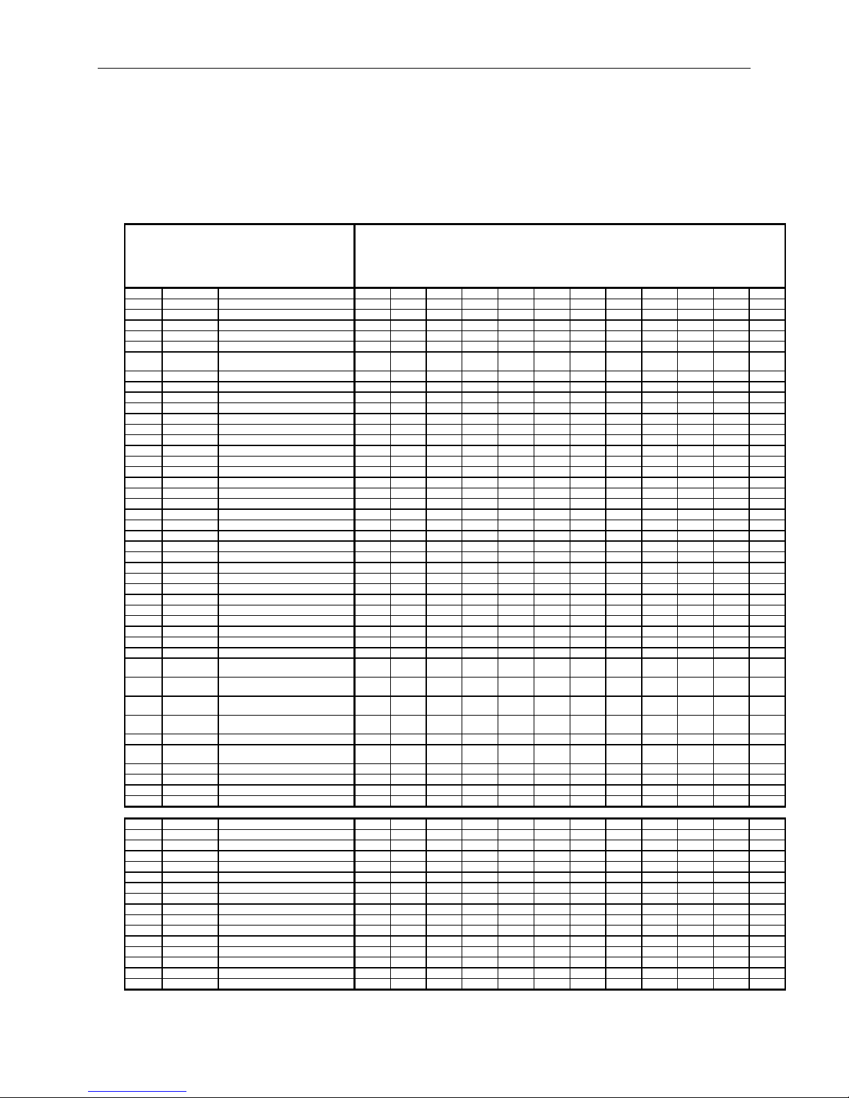
Table 13: Flat Panel Display Pinout
Mono
Mono
Mono
Color
Color
Color
Color
Color
Color
Color
Color
SS
DD
DD
TFT
TFT
TFT
TFT HR
STN SS
STN SS
Signal
Pin
Name Function
J4[1] +12V Power Supply
J4[2] +12V Power Supply
J4[3] GND Ground
J4[4] GND Ground
J4[5] +5V Power Supply
J4[6] +5V Power Supply
J4[7] ENAVEE Power sequencing control
J4[8] GND Ground
J4[9] FP0 Data Output D0 UD3 UD7 B0 B0 FB0 FB0 R1 R1 UR1 UR0 UR0
J4[10] FP1 “ “ D1 UD2 UD6 B1 B1 FB1 FB1 B1 G1 UG1 UG0 UG0
J4[11] FP2 “ “ D2 UD1 UD5 B2 B2 FB2 FB2 G2 B1 UB1 UB0 UB0
J4[12] FP3 “ “ D3 UD0 UD4 B3 B3 FB3 FB3 R3 R2 UR2 UR1 LR0
J4[13] FP4 “ “ D4 LD3 UD3 B4 B4 FB4 SB0 B3 G2 LR1 LR0 LG0
J4[14] FP5 “ “ D5 LD2 UD2 G0 B5 FB5 SB1 G4 B2 LG1 LG0 LB0
J4[15] FP6 “ “ D6 LD1 UD1 G1 B6 SB0 SB2 R5 R3 LB1 LB0 UR1
J4[16] FP7 “ “ D7 LD0 UD0 G2 B7 SB1 SB3 B5 G3 LR2 LR1 UG1
J4[17] FP8 “ “ LD7 G3 G0 SB2 FG0 B3 UG1 UB1
J4[18] FP9 “ “ LD6 G4 G1 SB3 FG1 R4 UB1 LR1
J4[19] FP10 “ “ LD5 G5 G2 SB4 FG2 G4 UR2 LG1
J4[20] FP11 “ “ LD4 R0 G3 SB5 FG3 B4 UG2 LB1
J4[21] FP12 “ “ LD3 R1 G4 FG0 SG0 R5 LG1 UR2
J4[22] FP13 “ “ LD2 R2 G5 FG1 SG1 G5 LB1 UG2
J4[23] FP14 “ “ LD1 R3 G6 FG2 SG2 B5 LR2 UB2
J4[24] FP15 “ “ LD0 R4 G7 FG3 SG3 R6 LG2 LR2
J4[25] FP16 “ “ R0 FG4 FR0 LG2
J4[26] FP17 “ “ R1 FG5 FR1 LB2
J4[27] FP18 “ “ R2 SG0 FR2 UR3
J4[28] FP19 “ “ R3 SG1 FR3 UG3
J4[29] FP20 “ “ R4 SG2 SR0 UB3
J4[30] FP21 “ “ R5 SG3 SR1 LR3
J4[31] FP22 “ “ R6 SG4 SR2 LG3
J4[32] FP23 “ “ R7 SG5 SR3 LB3
J4[33] GND Ground
J4[34] GND Ground
J4[35] SHFCLK Shift Clock.
J4[36] FLM First Line Marker.
J4[37] DE Display Enable or
J4[38] LP Latch Pulse.
J4[39] GND Ground
J4[40] ENABKL Enable Backlight. Can be
J4[41] DDCDATA Serial Data
J4[42] DDCCLK Serial Data
J4[43] +3V Power Supply
J4[44] +3V Power Supply
J5[1] +5V Power Supply
J5[2] GND Ground
J5[3] FP24 Data Output FR0
J5[4] FP25 “ “ FR1
J5[5] FP26 “ “ FR2
J5[6] FP27 “ “ FR3
J5[7] FP28 “ “ FR4
J5[8] FP29 “ “ FR5
J5[9] FP30 “ “ SR0
J5[10] FP31 “ “ SR1
J5[11] FP32 “ “ SR2
J5[12] FP33 “ “ SR3
J5[13] FP34 “ “ SR4
J5[14] FP35 “ “ SR5
J5[15] GND Ground
J5[16] +5V Power Supply
for LCD bias voltage
Pixel clock for flat panel data.
Flat panel equivalent of VSYNC.
M signal (ADCCLK) or BLANK#
Flat panel equivalent of HSYNC.
programmed for other functions.
8-bit
8-bit
16-bit
9-bit
12-bit
16-bit
18-bit
24-bit
36-bit
18-bit
24-bit
8-bit
(4bP)
16-bit
(4bP)
STN DD
8-bit
(4bP)
STN DD
16-bit
(4bP)
Color
STN DD
24-bit
VSBC-8 Reference Manual Reference – 29
Page 42

Video Interface
OMPATIBLE FLAT PANEL DISPLAYS
C
The following list of flat panel displays are reported to work properly with the Asiliant
Technologies 69030 video controller chip used on the VSBC-8:
• Sharp LQ057Q3DC02
• Sharp LQ084V1DG21
• Sharp LQ10D344
• Sharp LQ10D346
• Sharp LQ10D367
• Sharp LQ10D421
• Sharp LQ9D161
• Sharp LQ9D340
• Sharp LQ10D131
• Sharp LQ12S08
• Sharp LQ12S31
• Sharp LQ12S41
• Sharp LQ64D142
• Sharp LQ64D341
• Sharp LQ64D343
• Sharp LQ104V1DG11
• Sharp LM64K101
• Sharp LM64P101
• Sharp LM64P839
• Sharp LM32P10
• Sharp LM8V31
• Sharp LM64C35P
• NEC NL6448AC33-27
• NEC NL6448AC33-18
• NEC NL6448AC33-24
• LG Elec. LCA4VE02A
• LG Elec. LP104S2
• Samsung LT104V4-101
• Hitachi TX31D27VC1CAB
• Hitachi TX26D80VC1CAA
30 – Reference VSBC-8 Reference Manual
Page 43

Ethernet Interface
The VSBC-8 features an industry-standard 10baseT / 100baseTX Ethernet interface based on the
Intel 82559ER interface chip. While this interface is not NE2000 compatible, the 82559ER
series is widely supported. Drivers are readily available to support a variety of operating systems
such as QNX, VxWorks and other RTOS vendors.
Ethernet Interface
BIOS C
ONFIGURATION
The Ethernet interface shares PCI interrupt “INTC*” with the AGP video controller and slot 2.
The CMOS Setup screen is used to select the IRQ line routed to INTC*.
TATUS
S
LED
Two colored LEDs (D1) located next to the RJ-45 connector provide an indication of the
Ethernet status as follows:
Green LED (Link / Activity)
• ON Active Ethernet cable plugged into J2.
No Tx/Rx data activity.
• OFF Cable not plugged into J2
Cable not plugged into active hub
• BLINKING Active Ethernet cable plugged into J2.
Tx or Rx data activity detected on the cable
Yellow LED (Speed)
• ON 100baseTx (Fast) detected on Ethernet cable.
• OFF 10BaseTx (Slow) detected on Ethernet cable.
E
THERNET CONNECTOR
A board-mounted RJ-45 connector is provided to make connection with category 5 Ethernet
cable. The Ethernet controller will autodetect 10BaseT/100BaseTX connections.
Table 14: RJ45 Ethernet Connector
J2
Signal
Pin
Name Function
4 IGND Isolated Ground
5 IGND Isolated Ground
6 R– Receive Data –
3 R+ Receive Data +
7 IGND Isolated Ground
8 IGND Isolated Ground
2 T– Transmit Data –
1 T+ Transmit Data +
VSBC-8 Reference Manual Reference – 31
Page 44

Audio
Audio
The audio interface on the VSBC-8 is implemented using the Cirrus Logic CS4281 PCI based
audio controller and the CS4297A audio Codec ’97. This interface meets or exceeds Microsoft’s
PC 97, PC 98 and PC 99 audio performance requirements. Drivers are available for all Windows
based operating systems. To obtain the most current versions, consult the VSBC-8 Product
Support web page at www.versalogic.com/private/vsbc8support.asp.
J6 provides the low level stereo input and low level stereo output connection points. The outputs
will drive any standard “powered” PC speaker set. Also, TTL level up / down volume controls
are provided. An “up” pushbutton switch and a ‘down” pushbutton switch are normally
connected between the appropriate pins on the connector and the ground reference. Activation of
a switch results in the volume level stepping up or down.
S
The audio interface uses PCI interrupt “INTD*”. The CMOS Setup screen is used to select the
IRQ line routed to INTD*.
OFTWARE CONFIGURATION
XTERNAL CONNECTIONS
E
Connector J6 is configured so that a standard 4-pin CD-ROM audio connector can be used to
directly provide the low level stereo input.
Table 15: Audio Connector
J6
Signal
Pin
Name Function
1 VOL-DN Volume down switch input
3 GND Switch Ground
7 VOL-UP Volume up switch input
5 GND Switch Ground
2,4,6,8,11,
12,13,14,
AGND Audio Ground
9 R-OUT Right channel output
15 L-OUT Left channel output
10 R-IN Right channel input
16 L-IN Left channel input
32 – Reference VSBC-8 Reference Manual
Page 45

Watchdog Timer
A watchdog timer circuit is included on the VSBC-8 to reset the CPU or issue a NMI if proper
software execution fails or a hardware malfunction occurs.
E
NABLING THE WATCHDOG
To enable or disable the watchdog to reset the CPU, set or clear bit D0 in I/O port 0E0h (or
1E0h). When changing the contents of the register, make sure not to alter the value of the other
bits. It is recommend to refresh the watchdog prior to enabling or disabling the watchdog.
The following code example enables the watchdog reset:
in al,E0h
or al,01h
out E0h,al
To enable or disable the watchdog to issue an NMI, set or clear bit D1 in I/O per 0E0h (or 1E0h).
When charging the contents of the register, make sure not to alter the value of the other bits. It is
recommend to refresh the watchdog prior to enabling or disabling the watchdog. Bit D2 can be
read to determine if watchdog timer has expired.
Watchdog Timer
The following code example enables the watchdog NMI:
in al,E0h
or al,02h
out E0h,al
Note! The watchdog timer powers up and resets to a disabled state.
EFRESHING THE WATCHDOG
R
If the watchdog timer is enabled, software must periodically refresh the watchdog timer at a rate
faster than the timer is set to expire (1.0 sec minimum). Outputting a 5Ah to the Watchdog Timer
Hold-Off Register at 0E1h (or 1E1h) resets the watchdog time-out period, see page 49 for
additional information.
There is no provision for selecting a different timeout period using software.
The following code example refreshes the watchdog:
mov al,5Ah
out E1h,al
CPU Temperature Monitor
A thermometer circuit constantly monitors the die temperature of the CPU. This circuit can be
used to detect over-temperature conditions which can result from fan or heat sink failure or
excessive ambient temperatures.
CMOS Setup is used to set the temperature detection threshold. A status bit in the Special
Control Register can be read to determine if the die temperature is above or below the threshold.
The system can be configured to generate a Non-Maskable Interrupt (NMI) when the
temperature exceeds the threshold.
See page 48 for additional information.
VSBC-8 Reference Manual Reference – 33
Page 46

Analog Input
Analog Input
The VSBC-8 employ a multi-range, 12-bit A/D converter which will accept up to eight singleended input signals. The converter features fast 6 microsecond conversion time, with channel
independent input ranges of 0 to +5V, ±5V, 0 to +10V, and ±10V.
ARDWARE CONFIGURATION
H
There are no jumpers associated with the analog input circuitry.
E
XTERNAL CONNECTIONS
Single-ended analog voltages are applied to connector J10 as shown in the table below.
Table 16: Analog Input Connector
J10
Signal
Pin
Name Function
1 ADCH0 Channel 0 Analog Input
2 ADCH1 Channel 1 Analog Input
3 ADGND Analog Ground
4 ADCH2 Channel 2 Analog Input
5 ADCH3 Channel 3 Analog Input
6 ADGND Analog Ground
7 ADCH4 Channel 4 Analog Input
8 ADCH5 Channel 5 Analog Input
9 ADGND Analog Ground
10 ADCH6 Channel 6 Analog Input
11 ADCH7 Channel 7 Analog Input
12 ADGND Analog Ground
Note! Connector J10 also includes signals for the Opto 22 interface.
Warning! All analog inputs are fault protected to ±16V (board power on or off). Exceeding
these maximums can cause permanent damage to the A/D converter circuitry.
Such damage is not covered under warranty.
ALIBRATION
C
There are no calibration adjustments. Calibration, if desired, is accomplished by mathematical
transformation in software.
34 – Reference VSBC-8 Reference Manual
Page 47
Analog Input
NALOG CONTROL REGISTER
A
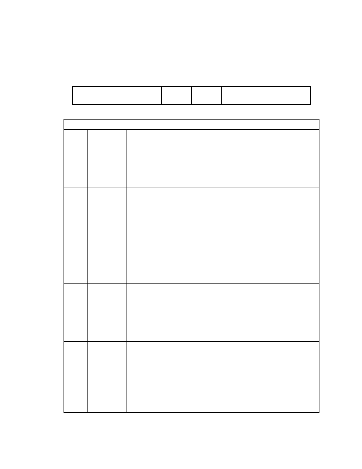
ACR (WRITE) 00E4h (or 1E4h via CMOS Setup)
D7 D6 D5 D4 D3 D2 D1 D0
PD1 PD0 ACQMOD RNG BIP A2 A1 A0
Table 17: Analog Control Register Bit Assignments
Bit Mnemonic Description
D7, D6 PD1, PD0 Clock and Power-Down Selection — These bits select the power savings
D5 ACQMOD Acquisition Mode — This bit selects the type of acquisition mode.
D4, D3 RNG, BIP Range and Polarity Selection — These bits select the input range and
D2-D0 A2, A1, A0 Input Channel Address — These bits select which input channel you wish to
mode and clock source for the A/D circuit.
PD1 PD0 Mode
0 0 Normal Operation / External Clock Mode
0 1 Normal Operation / Internal Clock Mode
1 0 Standby Power-Down (STBYPD)
1 1 Full Power-Down (FULLPD)
Note! STBYPD and FULLPD selections do not affect the clock mode.
ACQMOD = 0 Internal Acquisition. A write to the ACR register will initiate
an acquisition interval whose duration is internally timed. Conversion starts
when this six-clock-cycle acquisition interval (3.26µs) ends.
ACQMOD = 1 External Acquisition. Use this mode for precise control of the
sampling aperture and/or independent control of acquisition and conversion
times. The acquisition and start-of-conversion is controlled with two separate
writes to the ACR register. The first write, written with ACQMOD = 1, starts
and acquisition interval of indeterminate length. The second write, written with
ACQMOD = 0, terminates acquisition and starts conversion. However, if the
second write contains ACQMOD = 1, an indefinite acquisition interval is
restarted.
Note! The address bits for the input mux (A0–A2) must have the same values on the
first and second write pulses. Power-down mode bits (PD0, PD1) can assume new
values on the second write.
polarity on a channel-by-channel basis.
RNG BIP Input Range
0 0 0 to +5V
1 0 0 to +10V
0 1 ±5V
1 1 ±10V
Warning! The board can be damaged if voltages in excess of ±16V are applied.
convert.
A2 A1 A0 Channel
0 0 0 Channel 0
0 0 1 Channel 1
0 1 0 Channel 2
0 1 1 Channel 3
1 0 0 Channel 4
1 0 1 Channel 5
1 1 0 Channel 6
1 1 1 Channel 7
VSBC-8 Reference Manual Reference – 35
Page 48

Analog Input
IGITAL CONTROL
D
NALOG STATUS REGISTER
/ A
DCAS (READ/WRITE) 00E2h (or 1E2h via CMOS Setup)
D7 D6 D5 D4 D3 D2 D1 D0
Reserved Reserved Reserved Reserved Reserved DONE DIRHI DIRLO
Table 18: Digital Control / Analog Status Register Bit Assignments
Bit Mnemonic Description
D7-D3 Reserved Reserved — These bits have no function.
D2 DONE
Analog Input Conversion Complete — This status bit is used to
determine when it is OK to read data from the A/D converter.
DONE = 0 Conversion underway, data not yet available.
DONE = 1 Analog input conversion has completed. Valid data is
Note! This bit is not valid until an A/D conversion cycle has been triggered.
D1 DIRHI Direction Control for Opto 22 Digital I/O Hi Port — This bit controls the
input/output direction of the digital I/O signals DIO8–DIO15.
DIRHI = 0 Input
DIRHI = 1 Output
Note! See page 42 for further information.
D0 DIRLO Direction Control for Opto 22 Digital I/O Lo Port — This bit controls the
input/output direction of the digital I/O signals DIO0–DIO7.
DIRLO = 0 Input
DIRLO = 1 Output
Note! See page 42 for further information.
available to be read from the ADCLO and ADCHI registers.
Done is reset to “0” when a new conversion is started.
36 – Reference VSBC-8 Reference Manual
Page 49
Analog Input
ADC D
ATA HIGH REGISTER
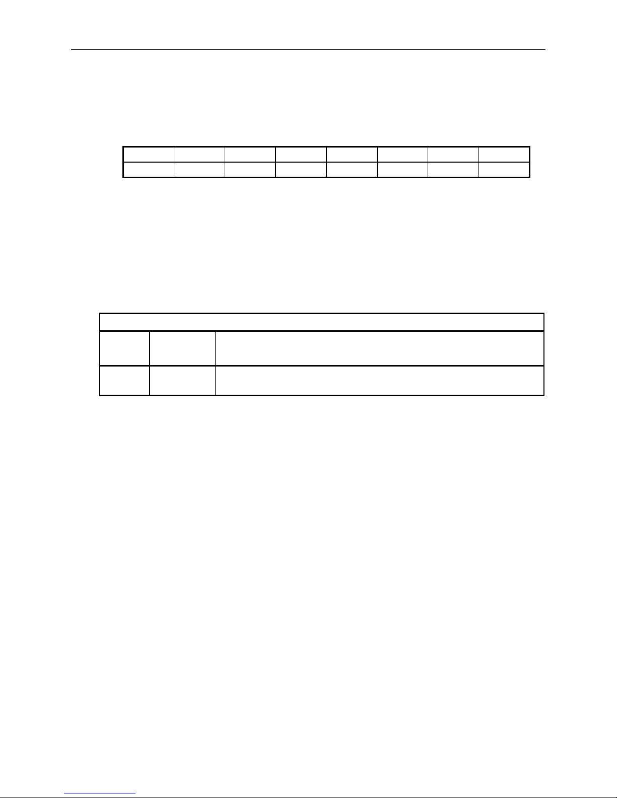
ADCHI (READ) 00E5h (or 1E5h via CMOS Setup)
D7 D6 D5 D4 D3 D2 D1 D0
D11 / 0 D11 / 0 D11 / 0 D11 / 0 D11 D10 D9 D8
The ADCHI register is a read register containing the upper 4 bits of data from the A/D
conversion results. It is used in conjunction with the ADCLO register to read the complete 12-bit
data word.
When reading data, it is normal convention to read the ADCLO register first, followed by the
ADCHI register.
Table 19: ADCHI Bit Assignments
Bit Mnemonic Description
D7-D4 D11 / 0
Sign Extension
(BIP = 0), in bipolar input mode, D11 is duplicated (sign extended) into
these four bits.
D3-D0 ADCDATA A/D Input Data (Most Significant Nibble) — These bits contain data
bits D11 through D8 of the conversion results.
— These four bits read as “0” in unipolar input mode
VSBC-8 Reference Manual Reference – 37
Page 50

Analog Input
ADC D
ATA LOW REGISTER
ADCLO (READ) 00E4h (or 1E4h via CMOS Setup)
D7 D6 D5 D4 D3 D2 D1 D0
D7 D6 D5 D4 D3 D2 D1 D0
The ADCLO register is a read register containing the lower 8 bits of data from the A/D
conversion results. It is used in conjunction with the ADCHI register to read the complete 12-bit
data word.
After a conversion is complete (as reported by the DONE bit in the ADCSTAT register) the
ADCLO register should be read first, followed by the ADCHI register. A word-wide input
instruction from the ADCLO register (in ax,dx) will fetch data from both registers in the proper
sequence.
The data registers are located on an even address boundary to facilitate efficient single-cycle
reading of the A/D data.
Table 20: ADCLO Bit Assignments
Bit Mnemonic Description
D7-D0 ADCDATA A/D Input Data (Least Significant Byte) — These bits contain data
bits D7 through D0 of the conversion results.
38 – Reference VSBC-8 Reference Manual
Page 51
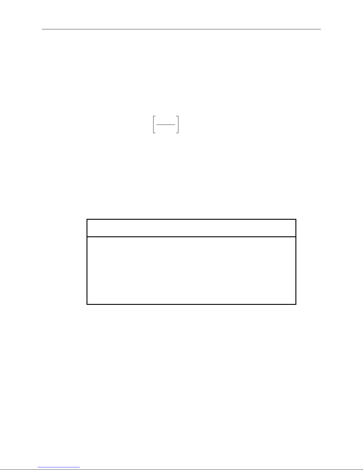
Analog Input
TWO’S C
OMPLEMENT DATA FORMAT
(±5V
AND
±10V O
NLY
)
The A/D converter translates applied analog voltages into 12-bit, two’s complement digital
words. The full analog input range is divided into 4096 steps. The output code (0000h) is
associated with a mid-range analog value of 0 Volts (ground).
The formulas for calculating analog or digital values are given by:
Digital =
Where:
Analog = Applied voltage
Digital = A/D Conversion Data
Step = 0.004882813 Volts (0 to +10V Range)
0.002441406 Volts (0 to +5V Range)
Analog
Step
Analog = Step Digital
x
Sample values are shown in the table below:
Table 21: Two’s Complement Data Format
±5V Input
Voltage
+5.000000 +10.000000 — — Out of range
+4.997559 +9.995117 07FFh 2047 Maximum positive voltage
+2.500000 +5.000000 0400h 1024 Positive half scale
+1.250000 +2.500000 0200h 512 Positive quarter scale
+0.002441 +0.004883 0001h 1 Positive 1 LSB
0.000000 0.000000 0000h 0 Zero (ground input)
–0.002441 –0.004883 FFFFh –1 Negative 1 LSB
–1.250000 –2.500000 FE00h –512 Negative quarter scale
–2.500000 –5.000000 FC00h –1024 Negative half scale
–5.000000 –10.000000 F800h –2048 Maximum negative voltage
±10V Input
Voltage Hex Decimal Comment
VSBC-8 Reference Manual Reference – 39
Page 52
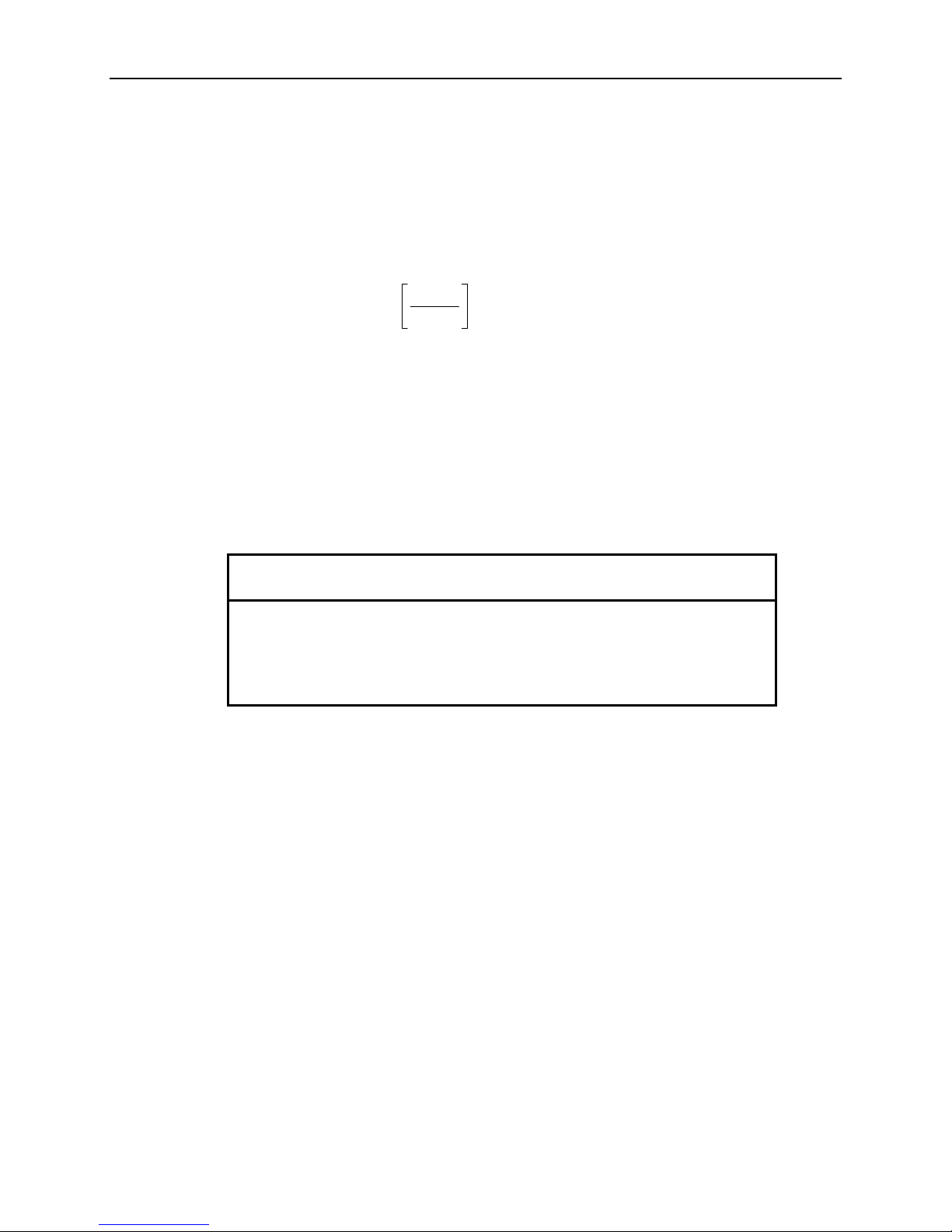
Analog Input
INARY FORMAT
B
(0
TO
+5V
AND 0 TO
+10V O
NLY
)
The full analog input range is divided into 4096 steps. The output code (0000h) is associated
with an analog input voltage of 0 Volts (ground). All codes are considered positive.
The formulas for calculating analog or digital values are given by:
Digital =
Where:
Analog = Applied voltage
Digital = A/D Conversion Data
Step = 0.002441406 Volts (0 to +10V Range)
0.001220703 Volts (0 to +5V Range)
Analog
Step
Analog = Step Digital
x
Sample values are shown in the table below:
Table 22: Binary Data Format
±5V Input
Voltage
+5.000000 +10.000000 — — Out of range
+4.998779 +9.997559 0FFFh 4095 Maximum voltage
+2.500000 +5.000000 0800h 2048 Half scale
+1.250000 +2.500000 0400h 1024 Quarter scale
+0.001220 +0.002441 0001h 1 1 LSB
0.000000 0.000000 0000h 0 Zero (ground input)
±10V Input
Voltage Hex Decimal Comment
NALOG INPUT CODE EXAMPLE
A
The following code example illustrates the procedure for reading a ±10V analog voltage from
channel 0:
OUT 0E4h,18h ;Select channel 0 and begin conversion
BUSY: IN AL,0E2h ;Get A/D status
AND AL,04h ;Isolate the DONE bit
JZ BUSY ;Loop back if conversion isn’t complete
DONE: MOV DX,00E4h ;Point to ADCLO register
IN AX,DX ;16-bit input reads ADCLO and ADCHI into AX
40 – Reference VSBC-8 Reference Manual
Page 53
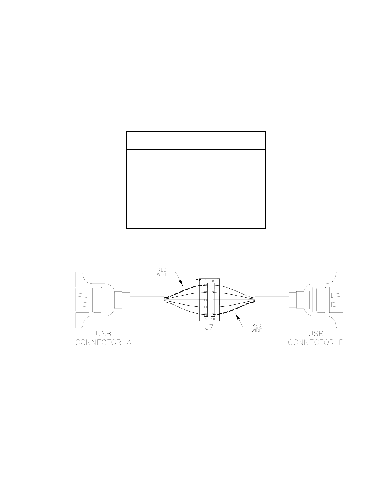
USB 1.1 Interface
A USB 1.1(Universal Serial Bus) connector provides a common interface to connect a wide
variety of keyboards, modems, mice, and telephony devices to the VSBC-8. With USB 1.1, there
is no need to have separate connectors for many common PC peripherals.
The USB 1.1 interface on the VSBC-8 is UHCI (Universal Host Controller Interface)
compatible, which provides a common industry software/hardware interface.
Table 23: USB 1.1 Interface Connector
J7
Signal
Pin
Name Function
1 USBPWR1 +5V (Protected)
2 USBP00 Channel 0 Data –
3 USBP01 Channel 0 Data +
4 GND1 Digital Ground
5 GND Cable Shield
6 GND Cable Shield
7 GND1 Digital Ground
8 USBP11 Channel 1 Data +
9 USBP10 Channel 1 Data –
10 USBPWR1 +5V (Protected)
USB 1.1 Interface
Warning! Connector J7 is not numbered in the conventional manner as most dual-row
headers. Care must be taken to attach the USB 1.1 adapter cables as shown below
to prevent voltage reversal.
Figure 6. USB 1.1 Connector Orientation Diagram
VSBC-8 Reference Manual Reference – 41
Page 54

Opto 22 (Digital I/O) Interface
Opto 22 (Digital I/O) Interface
The VSBC-8 includes a 16-channel digital I/O interface. The digital lines are grouped as two 8bit bi-directional ports. The direction of each port is controlled by software, and each signal is
pulled-up to +5V with a 10K ohm resistor.
The 24 mA source/sink drive and short protected outputs are an excellent choice for industrial
TTL interfacing, or they can be used to interface directly (plug compatible) with standard optoisolated modular I/O racks.
XTERNAL CONNECTIONS
E
Table 24: Digital I/O Connector
J10
Signal
Pin
Name Function
13 NC No Connection
14 GND Digital Ground
15 NC No Connection
16 GND Digital Ground
17 DIO0 OPTO 22 Module 15
18 GND Digital Ground
19 DIO1 OPTO 22 Module 14
20 GND Digital Ground
21 DIO2 OPTO 22 Module 13
22 GND Digital Ground
23 DIO3 OPTO 22 Module 12
24 GND Digital Ground
25 DIO4 OPTO 22 Module 11
26 GND Digital Ground
27 DIO5 OPTO 22 Module 10
28 GND Digital Ground
29 DIO6 OPTO 22 Module 9
30 GND Digital Ground
31 DIO7 OPTO 22 Module 8
32 GND Digital Ground
33 DIO8 OPTO 22 Module 7
34 GND Digital Ground
35 DIO9 OPTO 22 Module 6
36 GND Digital Ground
37 DIO10 OPTO 22 Module 5
38 GND Digital Ground
39 DIO11 OPTO 22 Module 4
40 GND Digital Ground
41 DIO12 OPTO 22 Module 3
42 GND Digital Ground
43 DIO13 OPTO 22 Module 2
44 GND Digital Ground
45 DIO14 OPTO 22 Module 1
46 GND Digital Ground
47 DIO15 OPTO 22 Module 0
48 GND Digital Ground
49 PWR +5V Rack Power*
50 GND Digital Ground
* Optional. Refer to jumper V4 on page 15.
Note! The digital signals on connector J10 are shared with the analog input interface.
42 – Reference VSBC-8 Reference Manual
Page 55
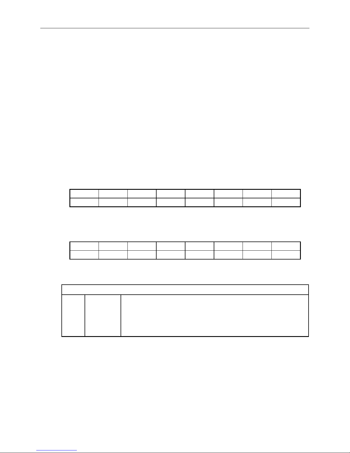
Opto 22 (Digital I/O) Interface
ACK POWER
R
When jumper V4 is installed, up to 250 mA can be drawn from J10 pin 49 to power the Opto 22
interface rack or other external equipment. The power output is protected by a self resetting
circuit breaker.
Warning! If the I/O rack is powered by a separate external supply, the power jumper on the
I/O rack or jumper V4 must be removed.
IGNAL DIRECTION
S
The 16 I/O signals are divided into two 8-bit I/O ports. The direction of each port is controlled
by the DIRHI and DIRLO bits in the DCAS register (see page 36).
IGITAL
D
I/O D
ATA PORTS
DIOHI (READ/WRITE) 00E7h (or 1E7h via CMOS Setup)
D7 D6 D5 D4 D3 D2 D1 D0
DIO15 DIO14 DIO13 DIO12 DIO11 DIO10 DIO9 DIO8
DIOLO (READ/WRITE) 00E6h (or 1E6h via CMOS Setup)
D7 D6 D5 D4 D3 D2 D1 D0
DIO7 DIO6 DIO5 DIO4 DIO3 DIO2 DIO1 DIO0
Table 25: Register Bit Assignments
Bit Mnemonic Description
D7-D0 DIO15–DIO8
DIO7–DIO0
Digital I/O Data — Data written to these register is driven onto the Opto 22
Digital I/O port signals when the port direction is set to output mode. When the
port is in input mode, these bits reflect the input state of the signal lines.
DIO = 0 Signal low (GND)
DIO = 1 Signal high (+5V)
Note! Opto 22 modules use inverted logic. An "on" module is a "0" logic level.
VSBC-8 Reference Manual Reference – 43
Page 56

Auxiliary Timer/Counter Channels
Auxiliary Timer/Counter Channels
The VSBC-8 includes three uncommitted 8254 type counter/timer channels for general
application program use. Control signals for the three channels are available on connector J8.
UMPER CONFIGURATION
J
Jumper V1 selects the clock source for channels 4 and 5. Options include:
• Internal 6 MHz timebase
• External clock from connector J8
• Cascading channels 4 and 5 together for 32-bit counter/timer operations
See page 14 for jumper configuration details.
E
XTERNAL CONNECTIONS
Table 26: Counter/Timer I/O Connector
OUNTER
C
J8
Signal
Pin
Name Function
1 OCTC3 CTC Channel 3 Output
2 GCTC3 CTC Chan 3 Gate Input
3 ICTC4 CTC Channel 4 Input
4 GND Digital Ground
5 OCTC4 CTC Channel 4 Output
6 GCTC4 CTC Chan 4 Gate Input
7 ICTC5 CTC Channel 5 Input
8 GND Digital Ground
9 OCTC5 CTC Channel 5 Output
10 GCTC5 CTC Chan 5 Gate Input
IMER REGISTERS
/ T
Table 27: Counter / Timer Registers
Mnemonic R/W Address Name
T3CNT R/W 0044h Timer 3 Count Load/Read
T4CNT R/W 0045h Timer 4 Count Load/Read
T5CNT R/W 0046h Timer 5 Count Load/Read
TCW W 0047h Timer Control Word
PERATION
O
Operational details for this industry standard 8254 type counter/timer chip are beyond the scope
of this manual. Register details, operational modes, and programming information can be
obtained from the VersaLogic website by downloading the 8254.PDF data sheet.
44 – Reference VSBC-8 Reference Manual
Page 57

PC/104 Expansion Bus
The VSBC-8 will accept up to four PC/104 and/or four PC/104-Plus expansion modules. Both
3.3V and 5.0V modules are supported.
RRANGING THE STACK
A
If PC/104-Plus modules will be used, they go on the stack first (closest to the VSBC-8 circuit
board). The first module is called "slot 0", the next module is "slot 1", and the third module is
"slot 2". Make sure to correctly configure the "slot position" jumpers on each PC/104-Plus
module to match it's physical position in the stack.
The BIOS automatically configures the I/O ports and Memory map allocation, including
allocation of interrupts.
PC/104 modules are stacked on top of the PC/104-Plus modules; 16-bit modules first followed
by 8-bit PC/104 modules. Lastly, non-standard modules which lack feedthrough connectors
should be assembled on top of the stack.
PC/104 Expansion Bus
Note Some modules may require –12V and/or –5V for correct operation. Check that the
proper connections to the 3-pin auxiliary power input connector (J3) are made if
your expansion module(s) use these voltages. See pages 11 and 16 for details.
ONFIGURATION
I/O C
PC/104 Modules
PC/104 I/O modules should be addressed in the 100h – 3FFh address range. Care must be taken
to avoid the I/O addresses shown in the On-Board I/O Devices table on page 46. These ports are
used by on-board peripherals and video devices.
PC/104-Plus Modules
PC/104-Plus modules do not use CPU I/O addressing. No configuration is necessary except to
jumper the expansion module for the correct stack position.
VSBC-8 Reference Manual Reference – 45
Page 58
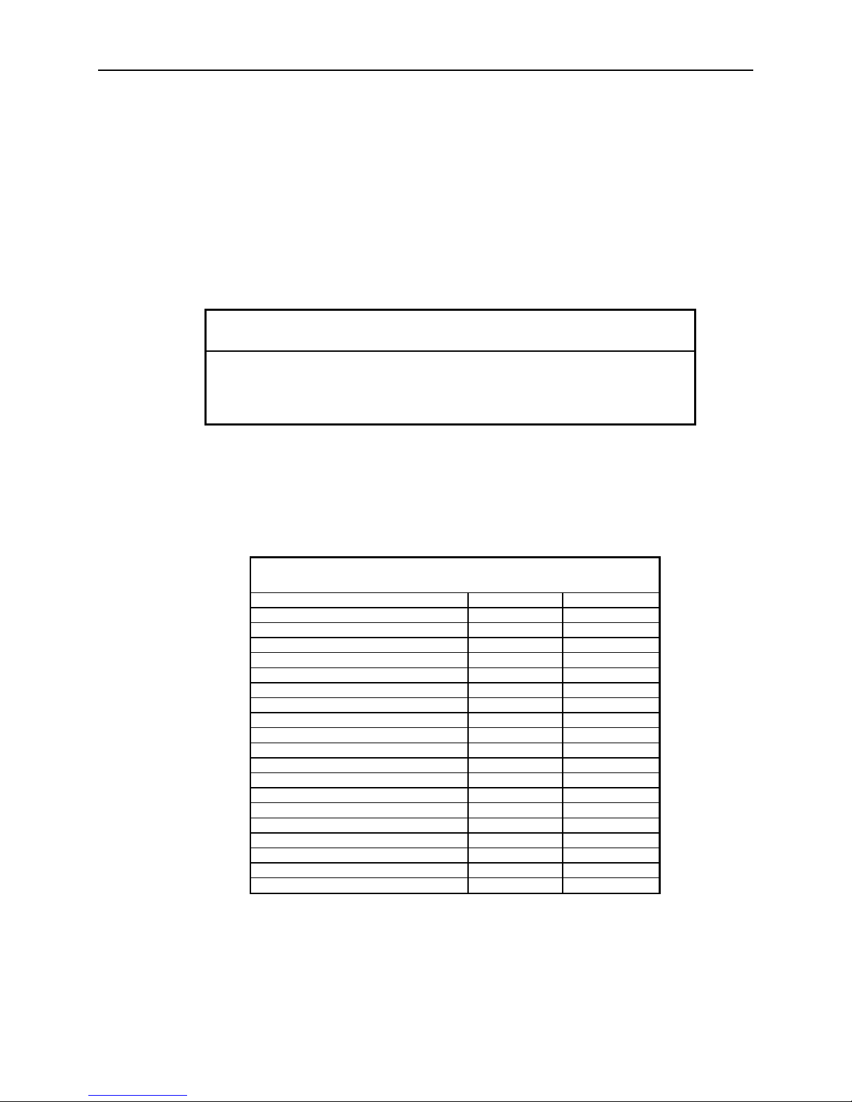
Memory and I/O Map
Memory and I/O Map
EMORY MAP
M
The lower 1 MB memory map of the VSBC-8 is arranged as shown in the following table.
Various blocks of memory space between C0000h and FFFFFh can be shadowed. CMOS setup is
used to enable or disable this feature.
Table 28: Memory Map
I/O M
Start
Address
F0000h FFFFFh System BIOS
E0000h
D0000h
C0000h CFFFFh Video BIOS
A0000h BFFFFh Video RAM
00000h 9FFFFh System RAM
AP
End
Address Comment
EFFFFh
DFFFFh
Flash Page, System BIOS, BBSRAM,DOC, BIOS Ext.
PC/104
The following table lists the common I/O devices in the VSBC-8 I/O map. User I/O devices
should be added using care to avoid the devices already in the map as shown below.
Table 29: On-Board I/O Devices
Standard
I/O Device
Auxillary Counter/Timer Channels 44h – 47h
Super I/O (COM 3 & 4) 02Eh-02Fh
Special Control Register 0E0h 1E0h
Watchdog Hold-Off Register 0E1h 1E1h
Digital Control / Analog Status Register 0E2h 1E2h
Map and Paging Control Register 0E3h 1E3h
Analog Control / ADC Low Register 0E4h 1E4h
ADC High Data Register 0E5h 1E5h
Digital I/O Low Data Register 0E6h 1E6h
Digital I/O High Data Register 0E7h 1E7h
Super I/O 15Ch-15Dh
Secondary Hard Drive Controller 170h – 177h
Primary Hard Drive Controller 1F0h – 1F7h
COM4 Serial Port 2E8h – 2EFh
COM2 Serial Port 2F8h – 2FFh
LPT1 Parallel Port 378h – 37Fh
SVGA Video 3B0h – 3DFh
COM3 Serial Port 3E8h – 3EFh
Floppy Disk Controller 3F0h – 3F7h
COM1 Serial Port 3F8h – 3FFh
I/O Addresses
Alternate *
I/O Addresses
Note The I/O ports occupied by on-board devices are freed up when the device is
disabled in CMOS Setup.
46 – Reference VSBC-8 Reference Manual
* User selectable via CMOS Setup.
Page 59
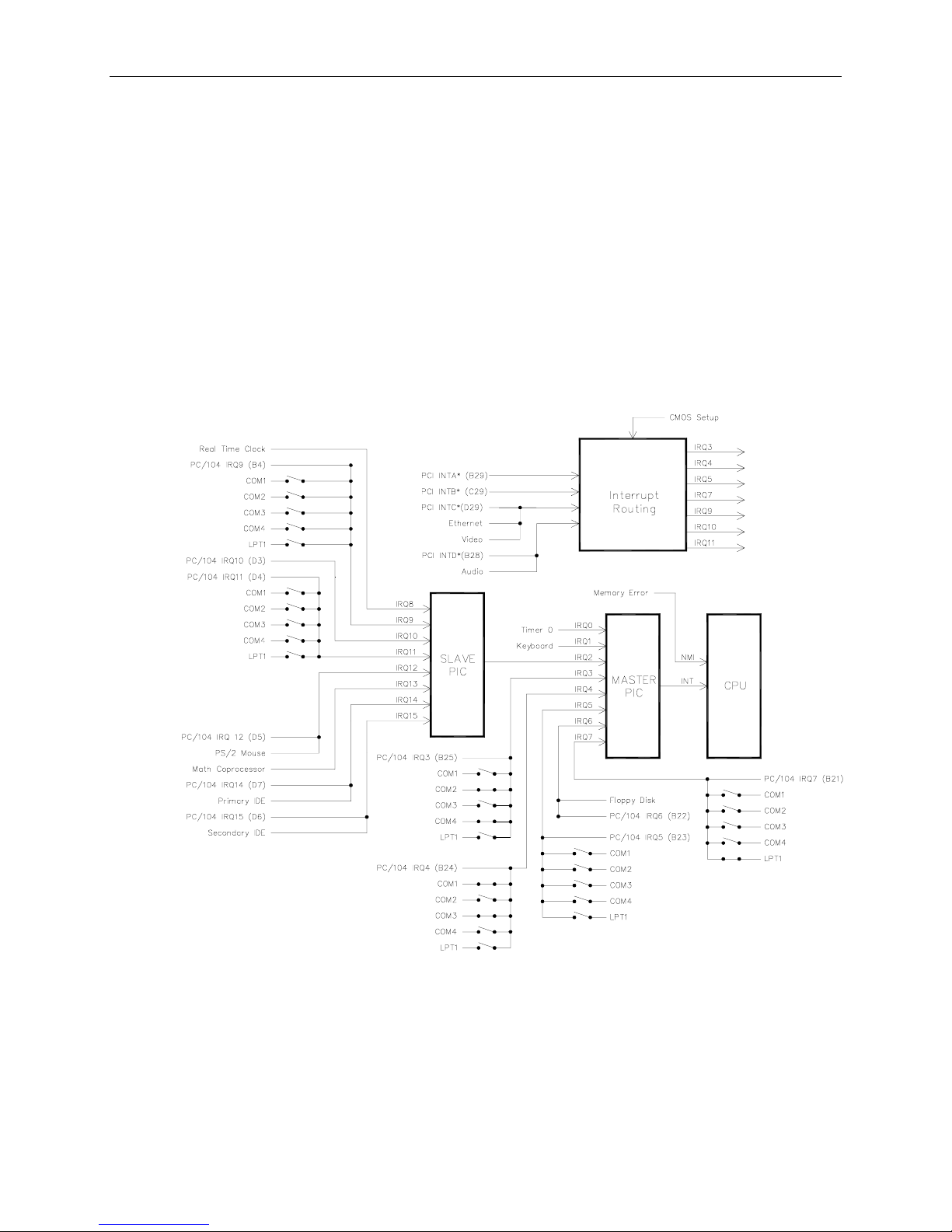
Interrupt Configuration
The VSBC-8 has the standard complement of PC type interrupts. Ten non-shared interrupts are
routed to the PC/104 bus, and up to four IRQ lines can be allocated as needed to PCI devices.
There are no interrupt configuration jumpers. All configuration is handled through CMOS setup.
The switches in the diagram below indicate the various CMOS Setup options. Closed switches
show factory default settings.
Note If your design needs to use interrupt lines on the PC/104 bus, we recommend using
IRQ5, IRQ9, and/or IRQ10.
Interrupt Configuration
VSBC-8 Reference Manual Reference – 47
Figure 7. Interrupt Circuit Diagram
Page 60
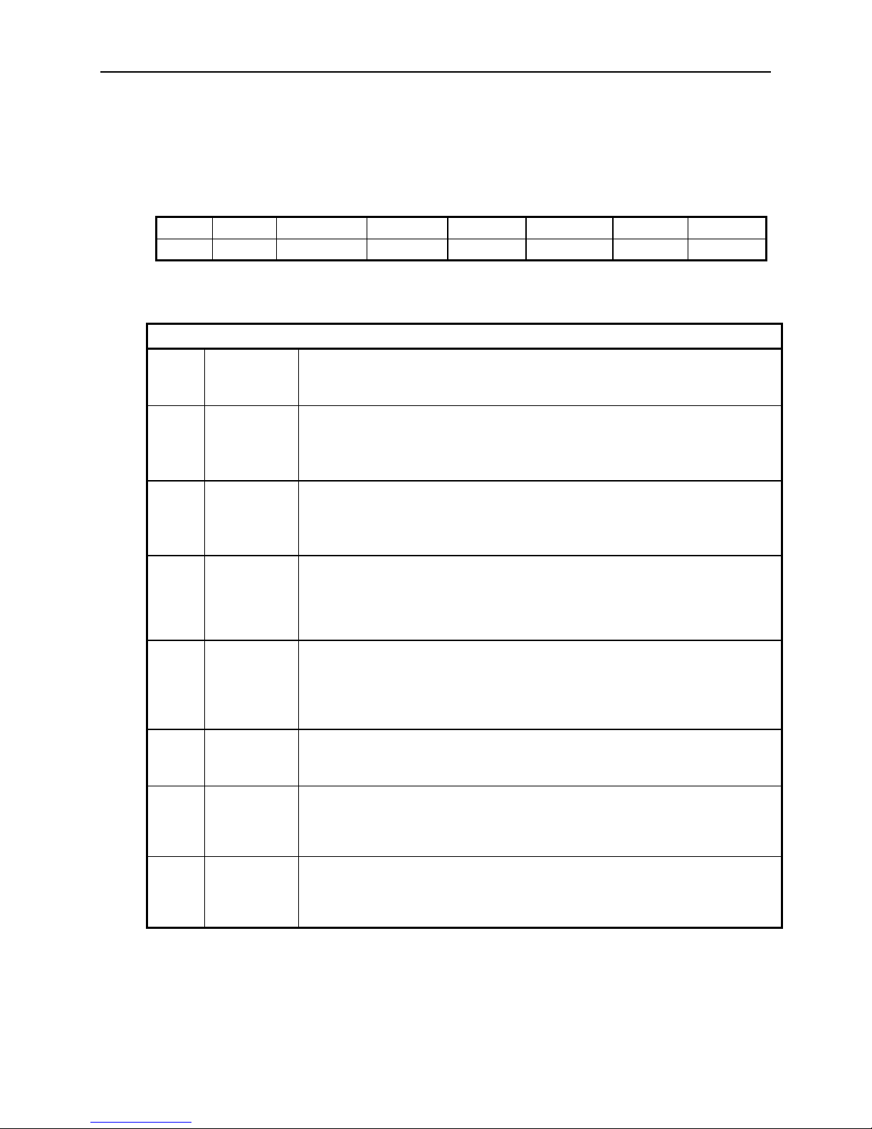
Special Control Register
Special Control Register
SCR (READ/WRITE) 00E0h (or 1E0h via CMOS Setup)
D7 D6 D5 D4 D3 D2 D1 D0
LED GPI OVERTEMP HDOGNMI THROTTLE WDOGSTAT WDOGNMI WDOGRST
Table 30: Special Control Register Bit Assignments
Bit Mnemonic Description
D7 LED Light Emitting Diode — Controls the programmable LED connector J9
LED = 0 Turns LED off.
LED = 1 Turns LED on.
D6 GPI General Purpose Input — Indicates the status of jumper V8[5-6].
GPI = 0 Jumper Out
GPI = 1 Jumper In
Note! This bit is a read-only bit
D5 OVERTEMP Temperature Status
TEMP = 0 CPU temperature is below value set in CMOS Setup
TEMP = 1 CPU temperature is above value set in CMOS Setup
Note! This bit is a read-only bit.
D4 HDOGNMI Non-Maskable Interrupt Enable — Controls the generation of Non-Maskable
interrupts whenever the CPU temperature sensor detects an over-temperature
condition.
NMIEN = 0 Disable
NMIEN = 1 Enable
D3 THROTTLE Processor Throttle Enable — Enables processor throttling. Throttling
percentage set in CMOS. (Always enabled on the VSBC-8b and VSBC-8e)
THROTTLE = 0 Disable
THROTTLE = 1 Enable
Note! This bit can only be cleared by resetting CPU on VSBC-8b and VSBC-8e.
D2 WDOGSTAT WDOG STATUS — Indicates if the watchdog timer has expired.
WDOGSTAT = 0 Timer has not expired.
WDOGSTAT = 1 Timer has expired.
D1 WDOGNMI Watch Dog Non-Maskable Interrupt Enable — Enables the generation of a
Non-maskable interrupt when the watchdog timer expires.
WDOGNMI = 0 Disables
WDOGNMI = 1 Enables
D0 WDOGRST Watch Dog Reset Enable — Enables and disables the watchdog timer reset
circuit.
WDOGEN = 0 Disables
WDOGEN = 1 Enables
— Indicates CPU temperature.
48 – Reference VSBC-8 Reference Manual
Page 61
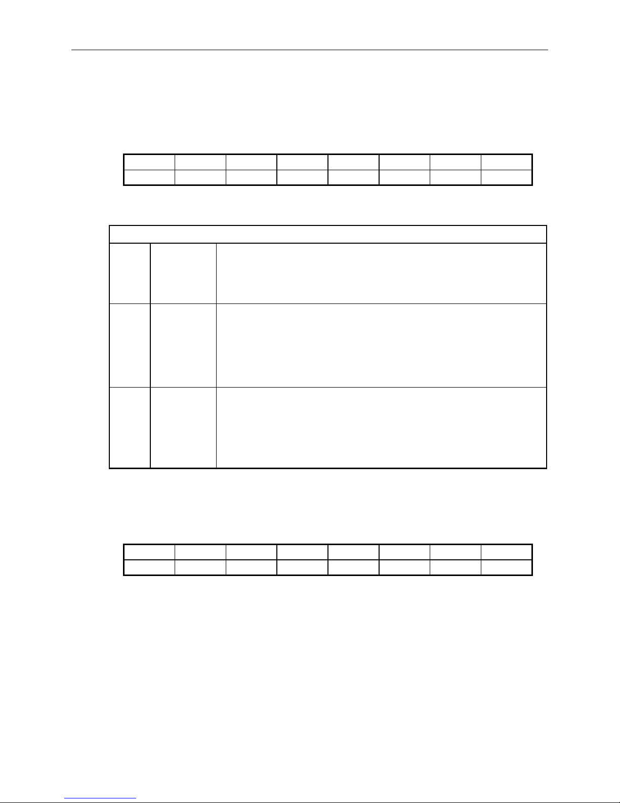
Revision Indicator Register
REVIND (READ ONLY) 00E1h (or 1E1h via CMOS Setup)
D7 D6 D5 D4 D3 D2 D1 D0
PC4 PC3 PC2 PC1 PC0 TC0 REV1 REV0
This register is used to indicate the revision level of the VSBC-8 product.
Bit Mnemonic Description
D7-D3 PC4-PC0 Product Code — These bits are hard coded to represent the product type. The
VSBC-8 will always read as 00001. Other codes are reserved for future products.
PC4 PC3 PC2 PC1 PC0 Product Code
00001 VSBC-8
Note! These bits are read-only.
D2 TC0 Throttling Code — This bit specifies how throttling is enabled at power-up and
reset.
0 = VSBC-8c No Throttling
VSBC-8d
1 = VSBC-8b Throttling set at 37.5%
VSBC-8e
Note! This bit is read-only.
D1-D0 REV1-REV0 Revision Level — These bits are represent the VSBC-8 circuit revision level.
REV1 REV0 Revision Level
0 0 Initial product release
0 1 Reserved
1 0 Reserved
1 1 Reserved
Note! These bits are read-only.
Revision Indicator Register
Watchdog Timer Hold-Off Register
WDHOLD (WRITE ONLY) 00E1h (or 1E1h via CMOS Setup)
D7 D6 D5 D4 D3 D2 D1 D0
01011010
A watchdog timer circuit is included on the
if proper software execution fails or a hardware malfunction occurs. The watchdog timer is
controlled by the SCR.
If the watchdog timer is enabled, software must periodically refresh the watchdog timer at a rate
faster than the timer is set to expire (1000 ms minimum). Writing a 5Ah to WDHOLD resets the
watchdog timeout period.
VSBC-8 Reference Manual Reference – 49
VSBC-8
board to reset the CPU and/or generate a NMI
Page 62
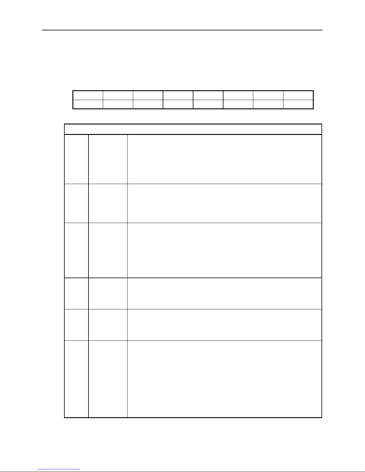
Map and Paging Control Register
Map and Paging Control Register
MPCR (READ/WRITE) 00E3h (or 1E3h via CMOS Setup)
D7 D6 D5 D4 D3 D2 D1 D0
FPGEN DPGEN SPGEN SB-SEL VB-SEL PG2 PG1 PG0
Table 31: Map and Paging Control Register Bit Assignments
Bit Mnemonic Description
D7 FPGEN FLASH Paging Enable — Enables a 64K page frame from E0000h to
EFFFFh. Used to gain access to the on-board FLASH memory.
FPGEN = 0 FLASH page frame disabled.
FPGEN = 1 FLASH page frame enabled.
Note! This bit is for factory use only. It is used to write user default CMOS setup
values to FLASH and to upgrade the system BIOS. When FPGEN = 1, the Page Select
bits are used to access various blocks within the FLASH.
D6 DPGEN DiskOnChip Enable — Enables a 64K page frame from E0000h to EFFFFh.
Used to gain access to the Disk on Chip
DPGEN = 0 DOC page frame disabled.
DPGEN = 1 DOC page frame enabled.
Note! The Page Select bits are not used when accessing the DOC.
D5 SPGEN Battery Backed Static RAM Paging Enable — Enables a 64K page frame
from E0000h to EFFFFh. Used to gain access to an optional Dallas
Semiconductor Battery-Backed Static RAM chip plugged into socket U20
(512KB max.)
SPGEN = 0 BBSRAM page frame disabled.
SPGEN = 1 BBSRAM page frame enabled
Note! When SPGEN = 1, the Page Select bits are used to access various 64K blocks
within the BBSRAM chip.
D4 SB-SEL System BIOS Selection — Indicates the status of jumper V8[1-2]
SB-SEL = 0 Jumper out, Secondary System BIOS selected.
SB-SEL = 1 Jumper in, Primary System BIOS selected.
Note! This bit is a read-only bit.
D3 VB-SEL Video BIOS Selection — Indicates the status of jumper V8[3-4]
VB-SEL = 0 Jumper out, Secondary Video BIOS selected.
VB-SEL = 1 Jumper in, Primary Video BIOS selected.
Note! This bit is a read-only bit.
D2-D0 PG2-PG0 Page Select — Selects which 64K block of FLASH or BBSRAM will be mapped
into the page frame at E0000h to EFFFFh
PG2 PG1 PG0 FLASH
0 0 0 000000h to 00FFFFh
0 0 1 010000h to 01FFFFh
0 1 0 020000h to 02FFFFh
0 1 1 030000h to 03FFFFh
1 0 0 040000h to 04FFFFh
1 0 1 050000h to 05FFFFh
1 1 0 060000h to 06FFFFh
1 1 1 070000h to 07FFFFh
Memory Range within
50 – Reference VSBC-8 Reference Manual
Page 63

Appendix A — Other References
PC Chipset Intel Corporation (developer.intel.com)
440 BX Chipset
Ethernet Controller Intel 82559ER (developer.intel.com)
Video Controller Chips and Technologies (Asiliant Technologies)
(www.Asiliant.com)
69030
A/D Converter Maxim Integrated Products, (www.maxim-ic.com)
Maxim 197
PC/104 Specification PC/104 Consortium, (www.controlled.com/pc104)
PC/104 Resource Guide
CPU Chips
Pentium III, Celeron Intel Corporation, (developer.intel.com)
PC/104-Plus Specification VersaLogic Corp., (www.versalogic.com)
PC/104 Resource Guide
General PC Documentation www.amazon.com
The Undocumented PC
A
Audio Controller Cirrus Logic, (www.cirrus.com)
CS4281/CS4297
VSBC-8 Reference Manual Appendix A — Other References – 51
 Loading...