

Page 1
VL-MPEe-V5
Reference
Manual
DOC. REV. 07/16/2015
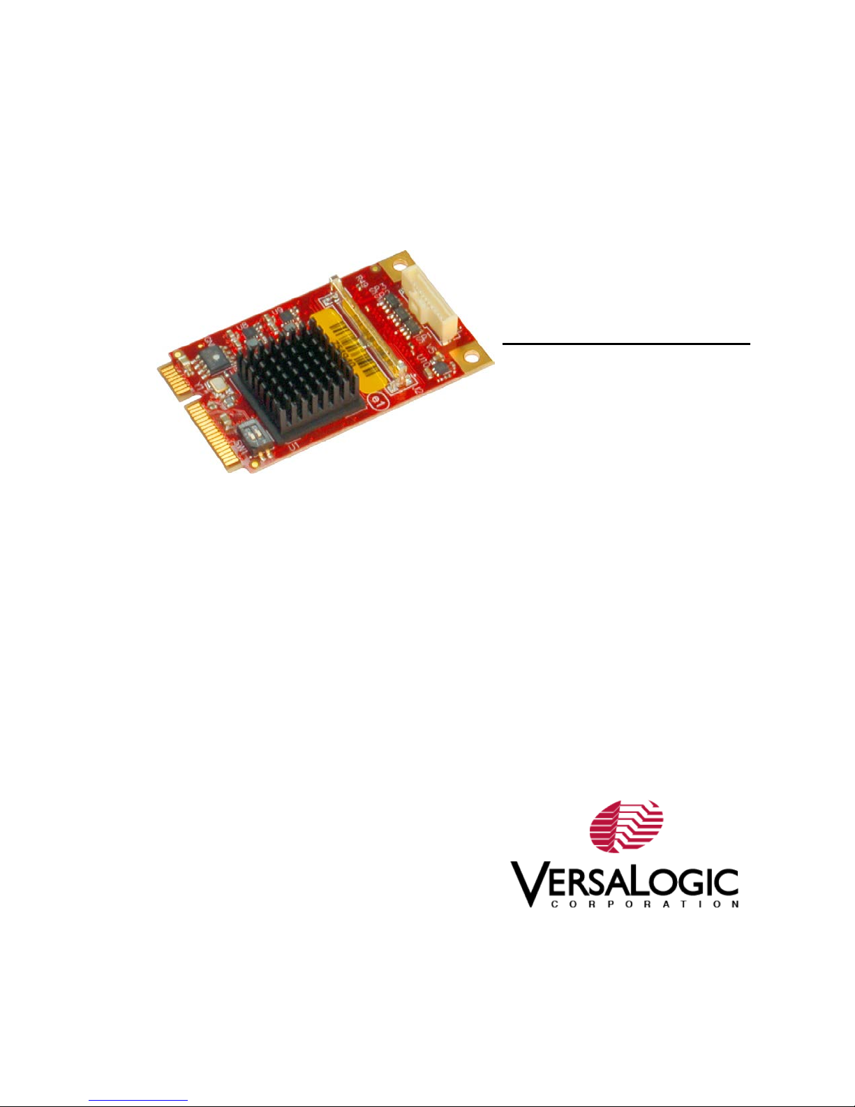
Mini PCIe Video Adapter
Page 2

WWW.VERSALOGIC.COM
12100 SW Tualatin Road
Tualatin, OR 97062-7341
(503) 747-2261
Fax (971) 224-4708
Copyright © 2015 VersaLogic Corp. All rights reserved.
Notice:
Although every effort has been made to ensure this document is error-free, VersaLogic makes no
representations or warranties with respect to this product and specifically disclaims any implied warranties
of merchantability or fitness for any particular purpose.
VersaLogic reserves the right to revise this product and associated documentation at any time without
obligation to notify anyone of such changes.
VL-MPEe-V5 Reference Manual ii
Page 3

Product Release Notes
Rev 1.1 – Second release. Replaced VGA connector with a PicoClasp connector for enhanced
reliability.
Rev 1.0 – Commercial Release.
Support Page
The VL-MPEe-V5 Support Page contains additional information and resources for this product including:
Operating system information and links to software drivers
Data sheets and manufacturers’ links for chips used in this product
Links to KnowledgeBase articles and product advisories
Knowledgebase
The VersaTech KnowledgeBase is a useful resource for resolving technical issues with your VersaLogic
product.
Customer Support
If you are unable to solve a problem after reading this manual, visiting the product support page, or
searching the KnowledgeBase, contact VersaLogic Technical Support at (503) 747-2261. VersaLogic
support engineers are also available via e-mail at Support@VersaLogic.com.
Repair Service
If your product requires service, you must obtain a Returned Material Authorization (RMA) number by
calling 503-747-2261. Provide the following information:
Your name, the name of your company, your phone number, and e-mail address
The name of a technician or engineer that can be contacted if any questions arise
The quantity of items being returned
The model and serial number (barcode) of each item
A detailed description of the problem
Steps you have taken to resolve or recreate the problem
The return shipping address
Warranty Repair All parts and labor charges are covered, including return shipping charges for
Non-warranty Repair All approved non-warranty repairs are subject to diagnosis and labor charges,
Note:
Mark the RMA number clearly on the outside of the box before returning.
UPS Ground delivery to United States addresses.
parts charges and return shipping fees. Specify the shipping method you
prefer and provide a purchase order number for invoicing the repair.
VL-MPEe-V5 Reference Manual iii
Page 4

Contents
Introduction ................................................................................................................... 1
Description ........................................................................................................... 1
Technical Specifications ...................................................................................... 1
Block Diagram ..................................................................................................... 2
Cautions .............................................................................................................. 3
Electrostatic Discharge ............................................................................. 3
Handling Care .......................................................................................... 3
Earth Ground Requirement ...................................................................... 3
Physical Layout ............................................................................................................. 4
Dimensions and Mounting .................................................................................... 4
VL-MPEe-V5 Mounting ............................................................................. 4
VL-MPEe-V5 Dimensions and Connectors ............................................... 4
Connector Functions and Interface Cables............................................... 5
Interfaces and Connectors ........................................................................................... 6
Video ................................................................................................................... 6
VGA Interface........................................................................................... 6
LVDS Flat Panel Display Connector ......................................................... 7
LVDS to VGA Adapter .............................................................................. 8
Appendix A – Technical Notes ................................................................................... 10
Drivers ............................................................................................................... 10
BIOS Configuration ............................................................................................ 10
Figures
Figure 1. Video Module Block Diagram ....................................................................... 2
Figure 2. Video Module Dimensions and Connectors .............................................. 4
Figure 3. VL-CBR-2014 LVDS to VGA Adapter Card ............................................... 8
Figure 4. LVDS Resolution Switch Positions .............................................................. 9
Tables
Table 1: Connector Functions and Interface Cables ................................................ 5
Table 2: Maximum Display Resolutions ...................................................................... 6
Table 3: J1 VGA Connector Pinout .............................................................................. 6
Table 4: LVDS Flat Panel Display Pinout ................................................................... 7
Table 5: LVDS Startup Resolution Switch Settings ................................................... 9
VL-MPEe-V5 Reference Manual
iv
Page 5

One VGA and one LVDS port
Board Size:
Video Output:
1
Description
The VL-MPEe-V5 is an extremely small and rugged video module based on the
industry-standard Mini PCIe module format. It pr ovides an easy and economical way to
add VGA and LVDS display outputs to an embedded computing solution. The board’s
features include the following:
Rugged, latching connectors
Industrial temperature operation
RoHS-compliant
Customization available
Introduction
The module features high-reliability design and construction. Careful part sourc ing and
US-based technical support ensure the highest pos sible q uality, r eliability, service, and
product longevity for this exceptional module.
This I/O board is compatible with a variety of popular x86 operating system s including
Windows, Windows Embedded, and Linux.
Technical Specifications
30.00 mm x 50.95 mm (Mini PCIe standard)
Storage Temperature:
-40° to +85 °C
Operating Temperature:
-40° to +8 5°C, derate -1.1 °C per 305m (1,000
ft.) above 2,300m (7,500 ft . )
Power Requirements: at +25°C running Windows 7
3.3 V @ 1.67 W (s uppl i ed from the Mini PCIe
socket, not incl udi ng LV DS 3.3V panel power
supply)
Video Controller:
Silicon Motion SM750. 2D Graphic Accelerator
Video core with 128-bit 2D graphic engine;
supports a single display, t wo cl oned di s pl ays,
or two simultaneous independent displays
See the VL-MPEe-V5 Data Sheet for complete specifications.
VGA: Up to 1920x1080 16-bit, 1440x960 32-bit
LVDS: Up to 1280x1024 18/24-bit
(see Table 2 for combi ned maximum
resolutions)
VRAM:
16 MB DDR SDRAM (32-bit) embedded in
SM750 controller
Mini PCIe Signal Type:
PCIe 1.1 signals from PCIe MiniCard bus
(USB and SMBus not used)
VL-MPEe-V5 Reference Manual
1
Page 6
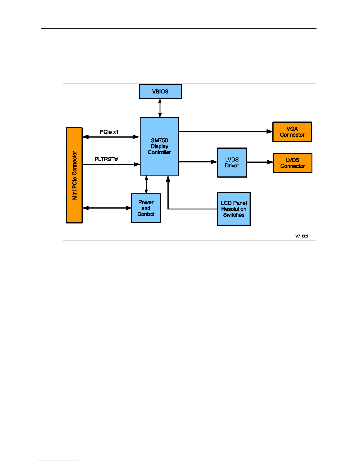
Block Diagram
Figure 1 shows a block diagram of the MPEe-V5 video module.
Introduction
Figure 1. Video Module Block Diagram
VL-MPEe-V5 Reference Manual 2
Page 7
Cautions
Electrostatic discharge (ESD) can damage circuit boards, disk drives and other
from the board and do not slide the bo ard over any surface.
After rem oving th e board from its protective wrapper, place the board on a
available.
The board should also be protected inside a closed metallic anti-static envelope
during shipment or storage .
Care must be taken when handling the board not to touch the exposed circuitry
with your fingers.
All mounting holes should be connected to earth ground (chassis ground). This
power supply.
ELECTROSTATIC DISCHARGE
Introduction
CAUTION:
components. The circuit board must only be handled at an ESD workstation. If
an approved station is not available, some measure of p rotection can be
provided by wearing a grounded antistatic wrist strap. Keep all plastic away
grounded, static-free surface, component side up. Use an antistatic foam pad if
HANDLING CARE
CAUTION:
EARTH GROUND REQUIREMENT
CAUTION:
provides proper grounding for ESD and EMI purposes. In portable applications,
the mounting holes should be connected to the ground reference of the system
VL-MPEe-V5 Reference Manual 3
Page 8
Be careful not to over tighten the nylon mounting screws. Optimum tightness is l lbf-in 0.1 Nm).
2
Dimensions and Mounting
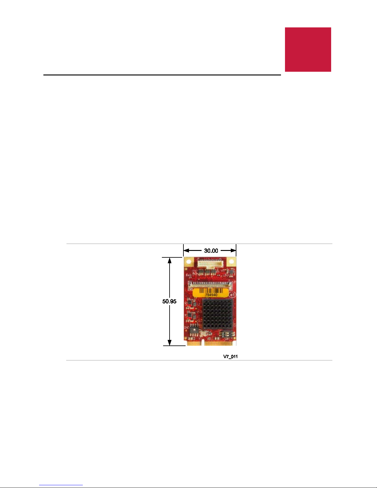
VL-MPEE-V5 MOUNTING
The VL-MPEe-V5 is a full size Mini PCIe card and needs to be mounted into a full size
Mini PCIe site. On VersaLog ic CPU boards, t he m odule is sec ur ed using two nylon
screws. VersaLogic supplies 2 mm nylon screws (VL-HDW-110) and 2.5 mm nylon
screws (VL-HDW-108). On non-VersaLogic CPU boards, mounting m ight be
accomplished using a latching system.
Note:
Physical Layout
VL-MPEE-V5 DIMENSIONS AND CONNECTORS
The VL-MPEe-V5 complies with MiniPCIe Mini Card (full size) dimensional standards.
Dimensions are given below to help with pre-production planning and layout. Figure 2
provides dimensions to help with pre-production planning and layout.
Figure 2. Video Module Dimensions and Connectors
(Not to scale. All dimensions in millimeters.)
VL-MPEe-V5 Reference Manual
4
Page 9
Physical Layout
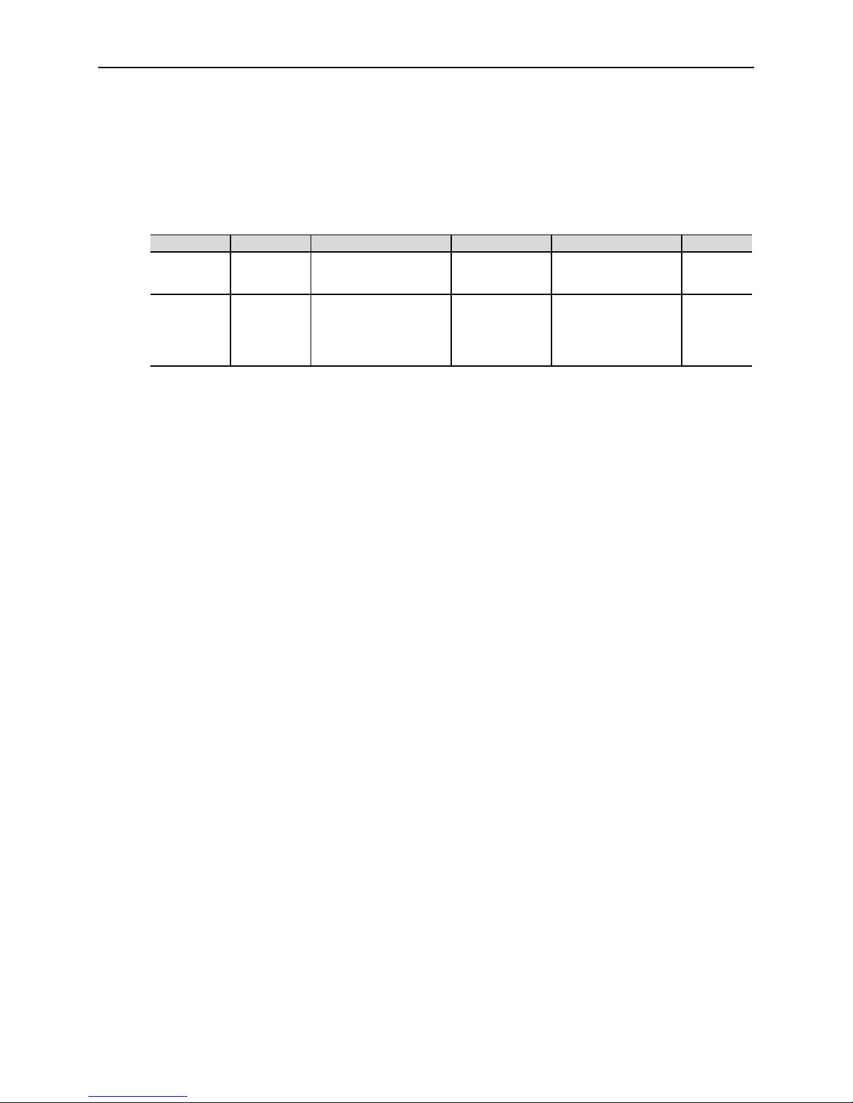
Connector
Function
Mating Connector
Transition Cable
Cable Description
Reference
12-inch VGA interface
(Note 2)
Notes:
CONNECTOR FUNCTIONS AND INTERFACE CABLES
Table 1 provides information about t he function, mating connector s, and transition
cables for VL-MPEe-V5 board connectors.
Table 1: Connector Functions and Interface Cables
J1 VGA
J2 LVDS
1. Attaches to opti onal V L-CBR-2014, LVDS to VGA adapter.
2. The CBR-2015 works with the LVDS to VGA adapter; the CB R-2016 does not.
Molex 501330-0500
pin/crimp
Hirose DF19G-20S-1C
(housing),
Hirose DF19-2830SCFA
x19 (crimp socket)
VL-CBR-1204
VL-CBR-2015
(Note 1)
--or--
VL-CBR-2016
cable, 12-pin PicoClasp
cable to 15-pin VGA
20-inch 18- or 24-bit
LVDS cable
Page 6
Page 7
VL-MPEe-V5 Reference Manual 5
Page 10

J1 Pin
Signal Name
Function
DB15 Pin
1
GND
Ground
6
2
VGA_RED
Red Video
1 3
GND
Ground
7 4
VGA_GREEN
Green Video
2 5
GND
Ground
8 6
VGA_BLUE
Blue Video
3 7
GND
Ground
5 8
VGA_HSYNC
Horizontal Sync
13
9
GND
Ground
10
10
VGA_VSYNC
Vertical Sync
11
CLK_VGA_DDC
DDC Serial Data Line Clock
VGA_DDC_DATA
12
3
Video
The Silicon Motion SM750 graphics controller has integrated high-per formance 2D
video, analog and flat panel output capability, and 16 MB of embedded VRAM.
The controller supports a single display, two cloned displays, or two simultaneous
independent displays. Table 2 lists the maximum resolut ions for each video channel
depending on the setup.
Interfaces and Connectors
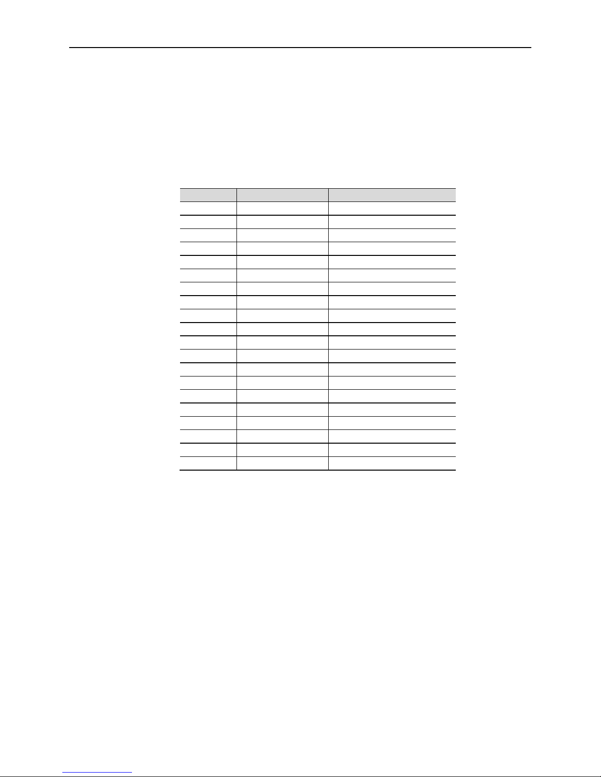
Table 2: Maximum Display Resolutions
Bits Per Pixel Channels Maximum CRT Resolution Maximum LCD Resolution
Single 1920 x 1080 1280 x 1024
16 bpp
32 bpp
Cloned 1280 x 1024 1280 x 1024
Dual 1280 x 1024 1280 x 1024
Single 1440 x 960 1280 x 1024
Cloned 1280 x 1024 1280 x 1024
Dual 1280 x 720 800 x 600
VGA INTERFACE
The VGA interface is a standar d analog output with a 12-pin PicoClasp connector. An
optional cable, part number VL-CBR-1204, is available to translat e VG A connector J1
into a standard 15-pin D-Sub SVGA connector.
Table 3 lists the function of each pin.
Table 3: J1 VGA Connector Pinout
14
15
12
DDC Serial Data Line
VL-MPEe-V5 Reference Manual
6
Page 11
Interfaces and Connectors
J2 Pin
Signal Name
Function
1
GND
Ground
2
NC
Not Connected
3
LVDSA3
Differential Data 3 (+)
4
LVDSA3#
Differential Data 3 (-)
5
GND
Ground
6
LVDSCLK0
Differential Clock (+)
7
LVDSCLK0#
Differential Clock (-)
8
GND
Ground
9
LVDSA2
Differential Data 2 (+)
10
LVDSA2#
Differential Data 2 (-)
11
GND
Ground
12
LVDSA1
Differential Data 1 (+)
13
LVDSA1#
Differential Data 1 (-)
14
GND
Ground
15
LVDSA0
Differential Data 0 (+)
16
LVDSA0#
Differential Data 0 (-)
17
GND
Ground
18
GND
Ground
19
+3.3V
+3.3V (Protected)
20
+3.3V
+3.3V (Protected)
LVDS FLAT PANEL DISPLAY CONNECTOR
The LVDS connector at location J2 is a 20-pin ver tical Hirose-style connector.
The flat panel interface can support 18 or 24 bits of RGB pixel data plus three bits of
timing control (HSYNC/VSYNC/DE) on the four differential data output pairs. The LVDS
interface supports a maximum res olution of 1280 x 1024.
Table 4: LVDS Flat Panel Display Pinout
The +3.3V power provided to pins 19 and 20 of J2 is protect ed by a softwarecontrollable power switch (1 A, maximum.). This switch is controlled by the FP_VDDEN
signal from the f lat panel interface in the video controller.
VL-MPEe-V5 Reference Manual 7
Page 12

Interfaces and Connectors
LVDS TO VGA ADAPTER
A VGA monitor can be attached to the J2 connect or using the VL-CBR-2014 LVDS to
VGA adapter card. Use the following procedure to do this.
1. Plug the "Host End" of the LVDS cable VL-CBR-2015 into connector J2.
2. Plug t he LVDS cable into connect or J 1 of the VL-CBR-2014 adapter card as
shown in Figure 3.
3. Attach the VGA monitor data cable t o c onnect or CN1 of the VL-CBR-2014 adapter
cable.
VL-MPEe-V5 Reference Manual 8
Figure 3. VL-CBR-2014 LVDS to VGA Adapter Card
Page 13

Interfaces and Connectors
Switch 1
Switch 2
Resolution
Off
Off
640 x 480 (default)
On
Off
800 x 600
Off
On
1024 x 768
On
On
1280 x 1024
LVDS Resolution Switch
The two switches at location SW1 provide several startup options for standard LVDS flat
panel types. If these options do not match the r equirements of the panel you are using,
contact Support@VersaLogic.com for a custom video BIOS. Table 5 lists the available
startup resolutions.
Table 5: LVDS Startup Resolution Switch Settin g s
Figure 4 shows the location of the switches as well as their Off/On positions.
Figure 4. LVDS Resolution Switch Positions
VL-MPEe-V5 Reference Manual 9
Page 14

A
Appendix A – Technical Notes
Drivers
Linux and Windows drivers for the VL-MPEe-V5 are available for download on the VL-
MPEe-V5 Product Support Page.
BIOS Configuration
The VL-MPEe-V5 can be installed on CPU boards with no graphics controller or with an
on-board graphics controller (either in a separ at e chip or int egrated into the processor).
In cases where an on-board graphics controller is to be used at the same time as the
VL-MPEe-V5, it is typically necessary to configure the BIOS of the CPU board so that it
recognizes the on-board controller as the prim ar y graphics device. This is because
when the CPU board detects the presence of an add-on g r aphics cont r oller , t he onboard controller is usually not fully init ia lized. Identifying the on-board device as the
primary graphics controller resolves this issue.
See the BIOS or CMOS Setup Reference article in the VersaT ec h KnowledgeBase for
your CPU board to determine how to configure the prim ar y graphics controller in the
BIOS, or contact VersaLogic Customer Support.
VL-MPEe-V5 Reference Manual
10
 Loading...