

Page 1

DOC. REV. 5/25/2017
Reference
Manual
VL-EBX-37
(Mamba)
Intel Core 2 Duo SBC with
Video, Ethernet, USB, Serial,
SATA, Audio, Analog + Digital
I/O, PCIe Mini Card, eUSB, and
SPX
Page 2

WWW.VERSALOGIC.COM
12100 SW Tualatin Road
Tualatin, OR 97062-7341
(503) 747-2261
Fax (971) 224-4708
Copyright © 2014-2017 VersaLogic Corp. All rights reserved.
Notice:
Although every effort has been made to ensure this document is error-free, VersaLogic makes no
representations or warranties with respect to this product and specifically disclaims any implied warranties
of merchantability or fitness for any particular purpose.
VersaLogic reserves the right to revise this product and associated documentation at any time without
obligation to notify anyone of such changes.
EBX-37 Reference Manual ii
Page 3

Product Release Notes
Models S and E
Rev 1.02 – Updated Web links
Rev 1.01 – Updated nominal battery voltage content.
Rev 1.0x – Commercial Release.
Rev 0.1x – Engineering build.
Models A and F
Rev 1.0x – Commercial Release. First dual-LVDS models. BIOS revision 6.5.102 release.
Support Page
The following resources are available for the VL-EBX-37:
Reference Manual (PDF format)
Data sheet
VersaAPI Installation and Reference Guide
This is a private page for VL-EBX-37 users that can be accessed only be entering this address directly. It
cannot be reached from the public VersaLogic website.
The VersaTech KnowledgeBase is an invaluable resource for resolving technical issues with your
VersaLogic product.
VersaTech KnowledgeBase
EBX-37 Reference Manual iii
Page 4

Contents
Introduction ..................................................................................................................... 1
Description .......................................................................................................................... 1
Technical Specifications ..................................................................................................... 2
VL-EBX-37 Block Diagram ............................................................................................... 3
Thermal Considerations ...................................................................................................... 4
CPU Die Temperature ........................................................................................... 4
Model Differences ................................................................................................. 4
RoHS-Compliance .............................................................................................................. 4
About RoHS ........................................................................................................... 4
Warnings ............................................................................................................................. 5
Electrostatic Discharge .......................................................................................... 5
Lithium Battery ...................................................................................................... 5
Handling Care ........................................................................................................ 5
Earth Ground Requirement .................................................................................... 5
Technical Support ............................................................................................................... 6
Repair Service ........................................................................................................ 6
Configuration and Setup .................................................................................................. 7
Initial Configuration ........................................................................................................... 7
Basic Setup ......................................................................................................................... 7
CMOS Setup ....................................................................................................................... 9
Operating System Installation ............................................................................................. 9
Physical Details .............................................................................................................. 10
Dimensions and Mounting ................................................................................................ 10
Hardware Assembly ............................................................................................. 13
Standoff Locations ............................................................................................... 13
External Connectors ......................................................................................................... 14
VL-EBX-37 Connector Locations – Top ............................................................ 14
VL-EBX-37 Connector Locations – Bottom ....................................................... 15
VL-EBX-37 Connector Functions and Interface Cables ..................................... 16
VL-CBR-5009 Connector Locations ................................................................... 17
VL-CBR-5009 Connector Functions ................................................................... 17
VL-CBR-4004 Connector Locations ................................................................... 18
Jumper Blocks .................................................................................................................. 19
Jumpers As-Shipped Configuration ..................................................................... 19
Jumper Summary ................................................................................................. 19
System Features ............................................................................................................. 20
Power Supply .................................................................................................................... 20
Power Connector (J6) .......................................................................................... 20
Power Requirements ............................................................................................ 20
Power Delivery Considerations ........................................................................... 21
EBX-37 Reference Manual iv
Page 5

Table of Contents
Lithium Battery .................................................................................................... 21
CPU ................................................................................................................................... 22
System RAM ..................................................................................................................... 22
Compatible Memory Modules ............................................................................. 22
RAM Size Limitation .......................................................................................... 22
SSDDR3 Dual Function Memory and Solid State Drive .................................... 22
CMOS RAM ..................................................................................................................... 22
Clearing CMOS RAM ......................................................................................... 22
CMOS Setup Defaults ...................................................................................................... 23
Default CMOS RAM Setup Values ..................................................................... 23
Saving CMOS Setup Parameters as Custom Defaults ......................................... 23
Primary and Backup BIOS ................................................................................................ 24
Real-time Clock ................................................................................................................ 24
Setting the Clock.................................................................................................. 24
Fan Tachometer Monitor .................................................................................................. 24
Fan Tachometer Read Code Example ................................................................. 24
Interfaces and Connectors .............................................................................................. 26
SATA Ports (J1, J7) .......................................................................................................... 26
USB (Multiple Connectors) .............................................................................................. 26
Video Interface (J11, J31, J33) ......................................................................................... 27
SVGA Output Connector (J11) ........................................................................... 27
LVDS Flat Panel Display Connector (J31, J33) .................................................. 28
Compatible LVDS Panel Displays ...................................................................... 29
Console Redirection ............................................................................................ 29
Ethernet Interface (J12, J15) ............................................................................................. 30
Ethernet Connectors ............................................................................................ 30
Status LED (J5) ................................................................................................... 31
PCI Express Mini Card (J14) ............................................................................................ 32
Expansion Bus (J16, J20/J21) ........................................................................................... 33
PC/104-Plus – PCI (J16) ..................................................................................... 33
PC/104 – ISA (J20/J21) ....................................................................................... 33
IRQ Support ......................................................................................................... 33
Digital I/O (J17) ................................................................................................................ 34
Digital I/O Port Configuration Using the SPI Interface ...................................... 35
Utility I/O (J18) ................................................................................................................ 40
Serial Ports (J18) .............................................................................................................. 41
COM Port Configuration ..................................................................................... 41
COM3 / COM4 RS-485 Mode Line Driver Control ........................................... 41
Serial Port Connectors ......................................................................................... 42
PS/2 Keyboard and Mouse (J18) ...................................................................................... 43
Programmable LED (J18) ................................................................................................. 43
External Speaker (J18) ...................................................................................................... 44
Push-Button Reset (J18) ................................................................................................... 44
Analog Input (J22) ............................................................................................................ 44
External Connections ........................................................................................... 45
Analog Input Using the SPI Interface .................................................................. 45
Analog Output (J22) ......................................................................................................... 47
Counter Timers (J22) ........................................................................................................ 48
EBX-37 Reference Manual v
Page 6

Table of Contents
SPX Expansion Bus (J23) ................................................................................................. 49
VersaLogic SPX Expansion Modules ................................................................. 49
SPI Registers ........................................................................................................ 50
Audio (J26) ....................................................................................................................... 53
eUSB Solid State Drive (J27) ........................................................................................... 53
System Interrupts and I/O Devices ................................................................................. 54
Interrupts ........................................................................................................................... 54
On-board I/O Devices ....................................................................................................... 55
Special Registers ............................................................................................................ 56
PLED and Product Code Register .................................................................................... 56
PLD Revision and Type Register ..................................................................................... 57
Special Control Register ................................................................................................... 58
Appendix A – References ................................................................................................ 59
Appendix B – Custom Programming .............................................................................. 60
PLD Interrupts .................................................................................................................. 60
Interrupt Control Register .................................................................................... 60
Interrupt Status Register ...................................................................................... 61
8254 Timer Control Register ............................................................................................ 62
8254 Timer Base Address ................................................................................................. 64
A/D and D/A Control/Status Register .............................................................................. 65
System Test Register ........................................................................................................ 65
EBX-37 Reference Manual vi
Page 7

Intel Core 2 Duo 2.26 GHz, 1066
Six USB 2.0 ports
1
Description
The VL-EBX-37 is a feature-packed single board computer designed for OEM control projects
requiring fast processing, industrial I/O, flexible memory options and designed-in reliability and
longevity (product lifespan). Its features include:
Introduction
MHz FSB, 3 MB L2 cache
Up to 8 GB DDR3 socketed
memory, two SO-DIMMs
Two Intel 82574IT-based Ethernet
interfaces, autodetect 10BaseT /
100BaseTX / 1000BaseT
Intel GMA 4500 MHD graphics
core
Two RS-232 (115 Kbps max.) and
two RS-232/422/ 485 COM ports
(921 Kbps max.)
Two SATA ports, 3 Gb/s
Industrial I/O
12-bit analog inputs and outputs
Eight analog (and eight optional)
inputs
Four analog (and four optional)
outputs
Thirty-two digital I/O lines
One eUSB bootable flash interface
One PCI Express Mini Card socket
SPX interface supports up to four external
SPI devices either of user design or any of
the SPX™ series of expansion boards,
with clock frequencies from 1-8 MHz
Intel High Definition Audio (HDA)
compatible
PS/2 keyboard and mouse support
PC/104-Plus (PCI + ISA) expansion
TVS devices for ESD protection
CPU temperature sensor
EBX standard 5.75” x 8.00” footprint
Field-upgradeable BIOS with OEM
enhancements
Customization available
The VL-EBX-37 is an EBX single board computer with an Intel Core 2 Duo processor. The
board is compatible with a variety of popular operating systems including Windows, Windows
Embedded, Linux, VxWorks and QNX.
The VL-EBX-37 features high-reliability design and construction, including voltage sensing reset
circuits and self-resetting fuses on the +5V and +3.3V supplies to the user I/O connectors.
VL-EBX-37 boards are subjected to 100% functional testing and are backed by a limited twoyear warranty. Careful parts sourcing and US-based technical support ensure the highest possible
quality, reliability, service and product longevity for this exceptional SBC.
The VL-EBX-37 is equipped with a multifunction utility cable (breakout board) that provides
standard I/O interfaces, including four COM ports, PS/2 mouse and keyboard, pushbutton reset,
programmable LED and speaker. Additional I/O expansion is available through the stackable PCI
and ISA connectors, PCI Express Mini Card socket, and SPX expansion interface.
EBX-37 Reference Manual 1
Page 8

Technical Specifications
Board Size:
Analog Output:
Specifications are typical at +25°C with +5V supply unless otherwise noted. Typical power is
computed as the mean value of the Idle and Maximum power specifications. All power
specifications represent operation at +25°C with +5V supply running Windows XP with 1 GB
RAM, dual Ethernet, keyboard, and mouse. Maximum power is measured with 95% CPU
utilization.
Introduction
EBX standard: 5.75” x 8” (146 mm x 203 mm )
Storage Temperature:
-40°C to 85°C
Operating Temperature:
VL-EBX-37S, A: 0°C to +60°C with heatsink/fan
VL-EBX-37E, F: -40°C to +85°C with
heatsink/fan
Power Requirements: (+5V with 1 GB RAM, two
network connections , keyboard, mouse, and VGA running
Windows XP)
VL-EBX-37S, A: Idle 2.4A (12W), Max 5A (25W)
VL-EBX-37E, F: Idle 2.2A (11W), Max 3.5A
(17.5W)
+3.3V or ±12V might be required by s ome
expansion modules
System Reset:
– Major power rails monitored by Super I/O chi p
– CPU and base board temperature m oni toring
– Fan monitor
DRAM:
Two SO -DIMM sockets, up to 8 GB DDR3
Dual function mem ory and s ol i d state drive
(SSDDR3) capability at SO-DIMM 1 (J13)
Video Interface:
Intel GMA 4500 MHD graphics core
Analog output for VGA
LVDS (one or two ports) output for TFT FPDs
Up to 1920x1200 (24 bits)
Up to 64 MB shared DRAM pre-allocated plus up
to 1700 MB using Intel DVMT
SATA Interface:
Two SATA 3 Gb/s ports
Flash Interface:
USB SSD interface (eUSB)
PCIe Mini Card socket
Ethernet Interface:
Two Intel 82574IT based 10BaseT / 100BaseTX
/ 1000BaseT Ethernet Controllers
Analog Input:
8 or 16-channel, 12-bit, single-ended, 100 Ksps,
channel independent input range: ±5, ± 10, or
unipolar 0 to +5V or 0 to +10V
4 or 8 -channel, 12-bit, single-ended, 100 K sps,
0 to 4.096V
COM1/2 Interface:
RS-232, 16C550 compatible, 115 k bps max., full
9-wire
COM3/4 Interface:
RS-232/422/485, 16C550 compatibl e, 921 Kbps
max., 4-wire RS-232
USB:
Eight USB 2.0. Six USB type A ports (on-board),
one channel on eUSB, and one on PCIe Mini
Card
Audio:
HD audio CODEC
Stereo Line In and Stereo Line Out
SPX:
Supports four external SPI chips of user design
or any SPX series expansion board
BIOS:
Phoenix Embedded BIOS© with StrongFrame®
Technology and OEM enhancements
Field upgradeable with Flash BIOS Update Utility
Bus Speed:
CPU FSB:VL-EBX-37S: 1.066 GHz;
VL-EBX-37E: 800 MHz
DDR3: VL-EBX-37S: 1066 MT/s;
VL-EBX-37E: 800 MT/s
USB 2.0: 480 Mbps
LPC: 33.33 MHz
PC/104 (ISA): 8.33 MHz
SPX: 8 MHz max.
Compatibility:
PC/104 – Partial com pl i ance
PC/104-Plus
Weight: (no memory installed)
VL-EBX-37S – 0.834 lbs (0.378 kg)
VL-EBX-37E – 0.832 lbs (0.377 kg)
VL-EBX-37A – 0.821 lbs (0.372 kg)
VL-EBX-37F – 0.828 lbs (0.375 kg)
Specifications are subject to change without notification.
EBX-37 Reference Manual 2
Page 9
VL-EBX-37 Block Diagram
Introduction
EBX-37 Reference Manual 3
Figure 1. VL-EBX-37 Block Diagram
Page 10

Thermal Considerations
CPU DIE TEMPERATURE
The CPU die temperature is affected by numerous conditions, such as CPU utilization, CPU
speed, ambient air temperature, air flow, thermal effects of adjacent circuit boards, external heat
sources, and many others.
The CPU is protected from over-temperature conditions by several mechanisms.
The CPU will automatically slow down by 50% whenever its die temperature exceeds +105°C.
When the temperature falls back below +105°C, the CPU resumes full-speed operation.
As a failsafe, if the CPU die temperature climbs above +115°C, the CPU will turn itself off to
prevent damage to the chip. Note that Intel does not warrant their CPUs in the event of this
occurrence.
M
ODEL DIFFERENCES
VersaLogic offers both commercial and industrial temperature models of the VL-EBX-37. The
basic operating temperature specification for both models is shown below.
Introduction
VL-EBX-37S, A: 0°C to +60°C free air, no airflow
VL- EBX-37E, F: -40°C to +85°C free air
To reliably function at extreme temperatures the extended temperature model specifications
deviate from the standard model in the following ways:
The DRAM interface is slowed. PC3-6400 memory runs at 600 MHz. PC3-8500 memory
runs at 800 MHz.
The DRAM refresh rates are doubled.
The Front Side Bus speed is reduced to 800 MHz.
Maximum processor speed is limited to 1200 MHz.
The graphics core is limited to 400 MHz.
RoHS-Compliance
The VL-EBX-37 is RoHS compliant.
ABOUT ROHS
In 2003, the European Union issued Directive 2002/95/EC regarding the Restriction of the use of
certain Hazardous Substances (RoHS) in electrical and electronic equipment.
The RoHS directive requires producers of electrical and electronic equipment to reduce to
acceptable levels the presence of six environmentally sensitive substances: lead, mercury,
cadmium, hexavalent chromium, and the presence of polybrominated biphenyls (PBB) and
polybrominated diphenyl ethers (PBDE) flame retardants, in certain electrical and electronic
products sold in the European Union (EU) beginning July 1, 2006.
VersaLogic Corp. is committed to supporting customers with high-quality products and services
meeting the European Union’s RoHS directive.
EBX-37 Reference Manual 4
Page 11

Warnings
ELECTROSTATIC DISCHARGE
Warning! Electrostatic discharge (ESD) can damage circuit boards, disk drives and other
After removing the board from its protective wrapper, place the board on a
Note The exterior coating on some metallic antistatic bags is sufficiently conductive to
Introduction
components. The circuit board must only be handled at an ESD workstation. If an
approved station is not available, some measure of protection can be provided by
wearing a grounded antistatic wrist strap. Keep all plastic away from the board and
do not slide the board over any surface.
grounded, static-free surface, component side up. Use an antistatic foam pad if
available.
The board should also be protected inside a closed metallic anti-static envelope
during shipment or storage.
cause excessive battery drain if the bag comes in contact with the bottom-side of
the VL-EBX-37.
ITHIUM BATTERY
L
Warning! To prevent shorting, premature failure or damage to the lithium battery, do not
place the board on a conductive surface such as metal, black conductive foam or
the outside surface of a metalized ESD protective pouch. The lithium battery may
explode if mistreated. Do not recharge, disassemble or dispose of in fire. Dispose
of used batteries promptly and in an environmentally suitable manner.
ANDLING CARE
H
Warning! Care must be taken when handling the board not to touch the exposed circuitry
with your fingers. Though it will not damage the circuitry, it is possible that small
amounts of oil or perspiration on the skin could have enough conductivity to cause
the contents of CMOS RAM to become corrupted through careless handling,
resulting in CMOS resetting to factory defaults.
ARTH GROUND REQUIREMENT
E
Warning! All mounting standoffs (eight on EBX and EPIC boards, four on PC/104 boards)
should be connected to earth ground (chassis ground). This provides proper
grounding for ESD and EMI purposes.
EBX-37 Reference Manual 5
Page 12
Technical Support
The VersaTech KnowledgeBase contains a wealth of technical information about VersaLogic
products, along with product advisories. Click the link below to see all KnowledgeBase articles
related to the VL-EBX-37.
If you have further questions, contact VersaLogic Technical Support at (503) 747-2261.
VersaLogic support engineers are also available via e-mail at Support@VersaLogic.com
REPAIR SERVICE
If your product requires service, you must obtain a Returned Material Authorization (RMA)
number by calling (503) 747-2261.
Introduction
VersaTech KnowledgeBase
.
Please provide the following information:
Your name, the name of your company, your phone number, and e-mail address
The name of a technician or engineer that can be contacted if any questions arise
Quantity of items being returned
The model and serial number (barcode) of each item
A detailed description of the problem
Steps you have taken to resolve or recreate the problem
The return shipping address
Warranty Repair All parts and labor charges are covered, including return shipping
charges for UPS Ground delivery to United States addresses.
Non-warranty Repair All non-warranty repairs are subject to diagnosis and labor charges,
parts charges and return shipping fees. Please specify the shipping
method you prefer and provide a purchase order number for invoicing
the repair.
Note: Please mark the RMA number clearly on the outside of the box before
returning.
EBX-37 Reference Manual 6
Page 13

2
Initial Configuration
The following components are recommended for a typical development system.
VL-EBX-37 computer
ATX power supply
LVDS display
USB keyboard
USB mouse
SATA hard drive
USB CD-ROM drive
DDR3 DRAM SO-DIMM module
The following VersaLogic cables are recommended.
VL-CBR-2010, 2011, or 2012 – LVDS cable
VL-CBR-0701 – SATA data cable
VL-CBR-0401 – ATX to SATA power cable
VL-CBR-2022 – Main power cable
Configuration and Setup
You will also need a Windows (or other OS) installation CD.
Basic Setup
The following steps outline the procedure for setting up a typical development system. The VLEBX-37 should be handled at an ESD workstation or while wearing a grounded antistatic wrist
strap.
Before you begin, unpack the VL-EBX-37 and accessories. Verify that you received all the items
you ordered. Inspect the system visually for any damage that may have occurred in shipping.
Contact Support@VersaLogic.com immediately if any items are damaged or missing.
Gather all the peripheral devices you plan to attach to the VL-EBX-37 and their interface and
power cables.
It is recommended that you attach standoffs to the board (see Hardware Assembly) to stabilize
the board and make it easier to work with.
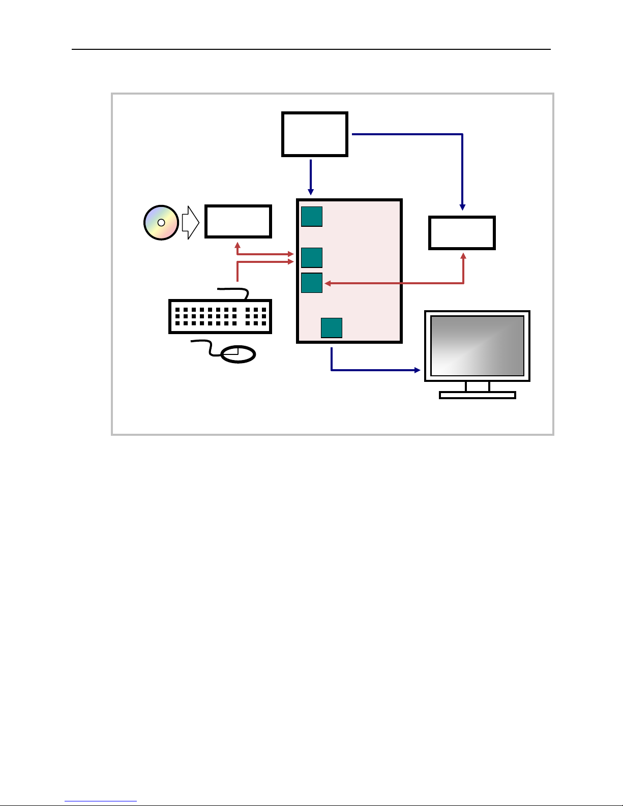
Figure 2 shows a typical start-up configuration.
EBX-37 Reference Manual 7
Page 14
OS Installation
CD-ROM
J6
VL-EBX-37
USB Keyboard
ATX
Power
SATA
CD-ROM
VL-CBR-201x LVDS
VL-CBR-0701
USB
USB
VL-CBR-2022
VL-CBR-0401
LVDS
USB
J31
J1/7
Supply
Configuration and Setup
Drive
Mamba
Hard Drive
and Mouse
Figure 2. Typical Start-up Configuration
1. Install Memory
Insert DDR3 DRAM module(s) into SO-DIMM sockets J13 and J29 and latch them into
place. If you install only one module, you must install it in the top socket, J13. If you use
DDR3 DRAM combined with a solid state drive (SSDDR3), you must install it in socket
J13.
2. Attach Cables and Peripherals
Plug the LVDS adapter cable VL-CBR-201x into socket J31 on the bottom of the board.
Attach the adapter cable to the LVDS display. (On models A and F, socket J33 can
alternately be used.)
Plug the USB CD-ROM drive, keyboard, and mouse into on-board USB ports (J2, J3, J4,
J8, J9, or J10).
Plug the SATA data cable VL-CBR-0701 into socket J1 or J7, and attach the SATA hard
drive to the cable.
Attach the ATX SATA power cable (VL-CBR-0401) to the ATX power supply and to
the SATA hard drive.
EBX-37 Reference Manual 8
Page 15

Configuration and Setup
3. Attach Power
Plug the power adapter cable VL-CBR-2022 into connector J6. Attach the motherboard
connector of the ATX power supply to the adapter.
4. Review Configuration
Before you power up the system, double check all the connections. Make sure all cables
are oriented correctly and that adequate power will be supplied to the VL-EBX-37 and
peripheral devices.
5. Power On
Turn on the ATX power supply and the flat panel display. If the system is correctly
configured, a video signal should be present.
6. Select a Boot Drive
During startup, press the B key to display the boot menu. Insert the OS installation CD in
the CD-ROM drive, and select to boot from the CD-ROM drive.
7. Install Operating System
Install the operating system according to the instructions provided by the OS
manufacturer. (See Operating System Installation.)
Note If you intend to operate the VL-EBX-37 under Windows XP or Windows XP
Embedded, be sure to use Service Pack 3 (SP3) and all updates for full support of
the latest hardware features.
CMOS Setup
See VersaLogic KnowledgeBase article VT1665 - EBX-37 Mamba CMOS Setup Reference for
complete information about the CMOS Setup parameters.
Operating System Installation
The standard PC architecture used on the VL-EBX-37 makes the installation and use of most of
the standard x86 processor-based operating systems very simple. The operating systems listed on
the VersaLogic OS Compatibility Chart
maker of the OS.
use the standard installation procedures provided by the
EBX-37 Reference Manual 9
Page 16
3
-0.20
0.00
–0.20
1.87
0.00
5.80
2.65
5.25
5.35
5.55
7.80
7.60
5.70
2.80
0.125 DIA x8
Use 3
standoffs
Dimensions and Mounting
The VL-EBX-37 complies with all EBX standards which provide for specific mounting hole and
PC/104-Plus stack locations as shown in the diagram below.
Physical Details
mm or #4
EBX-37 Reference Manual 10
Figure 3. VL-EBX-37 Dimensions and Mounting Holes
(Not to scale. All dimensions in inches.)
Page 17
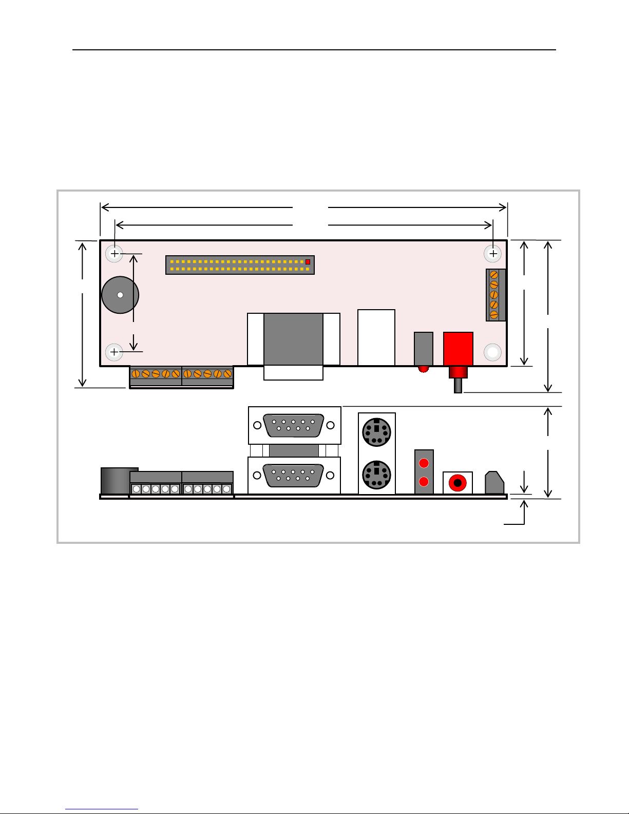
Physical Details
5.50
5.10
1.175
1.325
0.065
1.875
1.575
1.95
Caution The VL-EBX-37 must be supported at all eight mounting points to prevent
excessive flexing when expansion modules are mated and de-mated. Flex damage
caused by excessive force on an improperly mounted circuit board is not covered
under the product warranty.
EBX-37 Reference Manual 11
Figure 4. VL-CBR-5009 Dimensions and Mounting Holes
(Not to scale. All dimensions in inches.)
Page 18
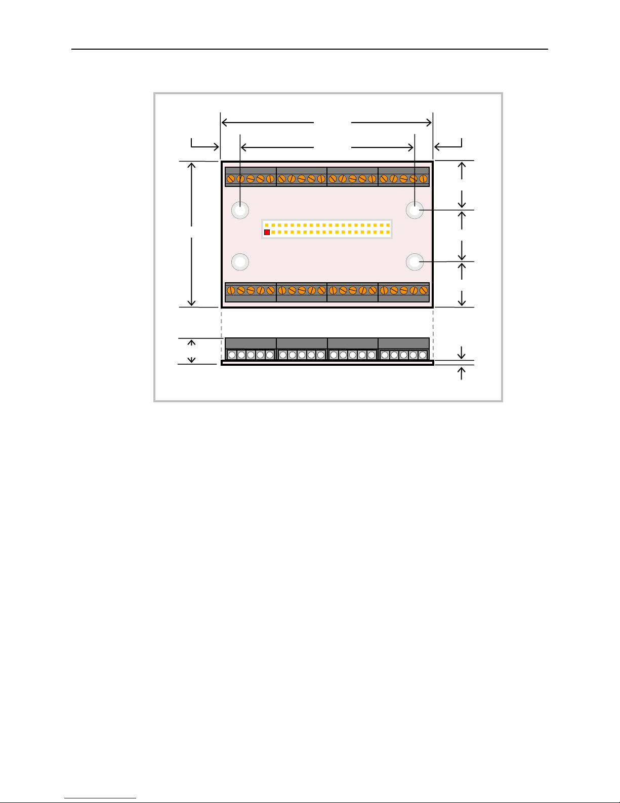
Physical Details
J1 J2 J3 J4
J6 J7 J8 J9
J5
+ + +
+
2.38
2.87
0.25
0.25
0.40
1.95
0.70
0.63
0.62
0.06
Figure 5. VL-CBR-4004 Dimensions and Mounting Holes
(Not to scale. All dimensions in inches.)
EBX-37 Reference Manual 12
Page 19
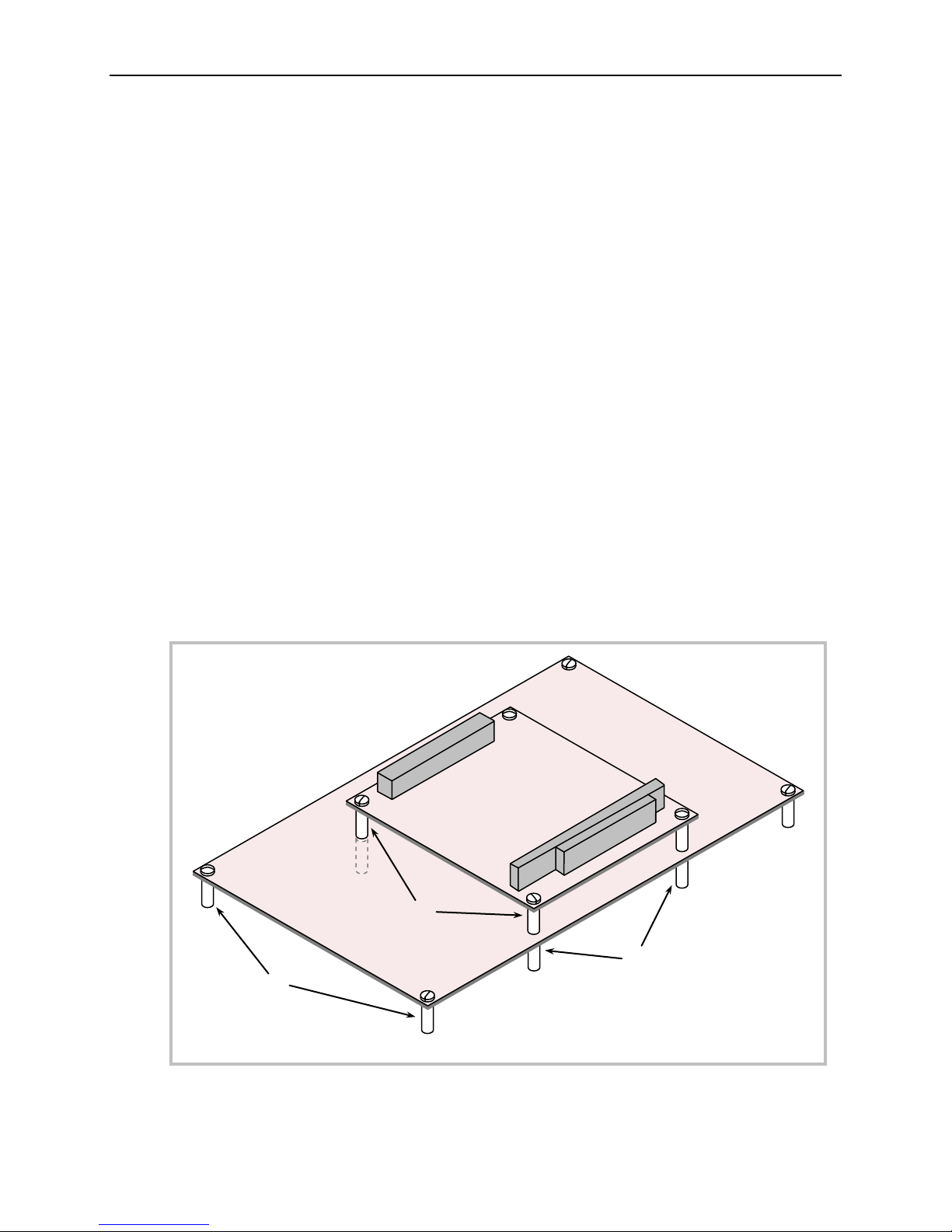
Physical Details
A
B
C
HARDWARE ASSEMBLY
The VL-EBX-37 mounts on four hardware standoffs using the corner mounting holes (A). These
standoffs are secured to the underside of the circuit board using pan head screws.
Four additional standoffs (B) must be used under the circuit board to prevent excessive flexing
when expansion modules are mated and separated. These are secured with four male-female
standoffs (C), threaded from the top side, which also serve as mounting struts for the PC/104
stack.
The entire assembly can sit on a table top or be secured to a base plate. When bolting the unit
down, make sure to secure all eight standoffs (A and B) to the mounting surface to prevent
circuit board flexing.
An extractor tool is available (part number VL-HDW-203) to separate the PC/104 modules from
the stack.
Note Standoffs and screws are available as part number VL-HDW-105 (metric thread)
or VL-HDW-106 (English thread).
Note All eight mounting standoffs should be connected to earth ground (chassis
ground). This provides proper grounding for ESD and EMI purposes.
TANDOFF LOCATIONS
S
EBX-37 Reference Manual 13
Figure 6. Standoff Locations
Page 20
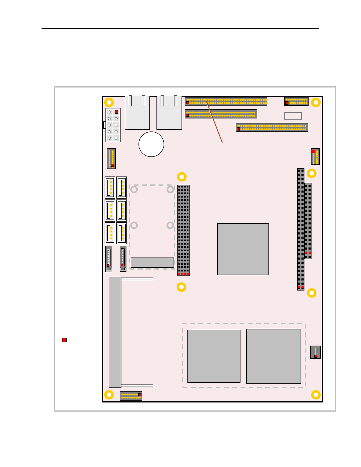
External Connectors
J16
PCI
J20-21
ISA
Battery
J6
Power
J12
J4, J10
, USB4
J3, J9
, USB3
J2, J8
, USB1
J1, J7
SATA1, SATA0
J18 – User I/O
J17
Digital
J22 – Analog I/O, Timers
J23 – SPX
CPU – Heatsink – Fan
J5
Ethernet LED
J25
Fan
J26
Audio
J13
SO
(DDR3 or
SSDDR3)
J15
J11 – SVGA
J14
PCIe Mini Card
= Pin 1
J19
VL-EBX-37 CONNECTOR LOCATIONS – TOP
Physical Details
USB5
USB2
USB0
Ethernet
Ethernet
I/O
Intel ICH9M
EBX-37 Reference Manual 14
-DIMM 1
Intel GM45
Figure 7. VL-EBX-37 Connector Locations - Top
Intel Core 2 Duo
(P8400)
Page 21
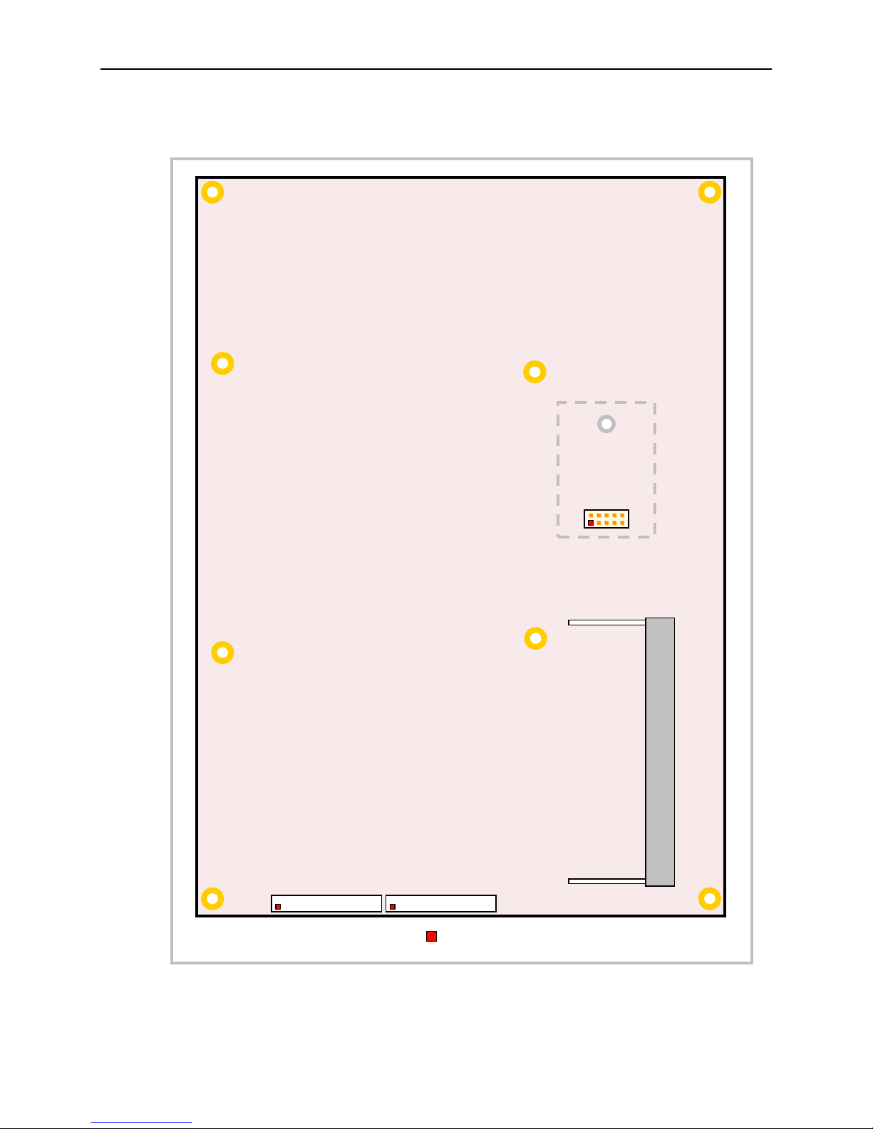
VL-EBX-37 CONNECTOR LOCATIONS – BOTTOM
J29
DIMM 2
(DDR3)
J31 – LVDS
J27 – eUSB
= Pin 1
J33 – Dual Link
High Res LVDS
Models A & F
Physical Details
EBX-37 Reference Manual 15
SO-
Figure 8. VL-EBX-37 Connector Locations - Bottom
Page 22

Physical Details
Connector1
Function
Mating Connector
Transition
Cable
Cable Description
Pin 1 Location2
x coord. y coord.
Page
J1
SATA 1
Standard SATA
VL-CBR-0701 or
VL-CBR-0401
500 mm (19.75”) 7-pin,
SATA power adapter
-0.037
3.675
26
J2
USB 0
Standard USB Type A
—
—
0.027
4.268
26
J3
USB 2
Standard USB Type A
—
—
0.027
4.978
26
J4
USB 5
Standard USB Type A
—
—
0.027
5.688
26
J5
Ethernet LED
—
—
—
0.004
6.063
31
J6
Main Power Input
(EBX compliant)
Molex 39-01-2100
Molex 39-00-0059 (10 ea.)
VL-CBR-2022
6” ATX to EPIC power
cable
0.157
7.341
20
J7
SATA 0
Standard SATA
VL-CBR-0701;
VL-CBR-0401
Refer to J1 (SATA 1)
0.318
3.675
26
J8
USB 1
Standard USB Type A
—
—
0.342
4.268
26
J9
USB 3
Standard USB Type A
—
—
0.342
4.978
26
J10
USB 4
Standard USB Type A
—
—
0.342
5.688
26
J11
SVGA Video
FCI 89361-712LF or
VL-CBR-1201
12" 12-pin 2 mm IDC
VGA
0.842
-0.035
27
J12
Gigabit Ethernet 1
RJ45
—
—
0.665
7.280
30
J13
SO-DIMM 1
(DDR3 RAM or SSDDR3)
—
—
0.216
1.599
22
J14
PCIe Mini Card
— — —
0.622
3.423
32
J15
Gigabit Ethernet 2
RJ45
—
—
1.632
7.280
30
J16
PC/104-Plus
AMP 1375799-1
—
—
2.112
3.100
33
J17
Digital I/O 1-32
FCI 89361-340LF
VL-CBR-4004A
12” 2 mm 40-pin to 40VL-CBR-4004 board
2.178
7.254
34
J18
COM1-4, PLED,
Button, Speaker
FCI 89361-350LF
VL-CBR-5009A
18” 2 mm 50-pin to 50-
2.179
7.605
40
J19
Factory Use Only
— —
J20-J21
PC/104
AMP 1375795-2
—
—
5.050
2.700
33
J22
Analog I/O, Timers
FCI 89361-340LF
VL-CBR-4004A
12” 2 mm 40-pin to 40VL-CBR-4004 board
3.574
6.901
44
J23
SPX
FCI 89361714LF
VL-CBR-1401;
VL-CBR-1402
2 mm 14-pin IDC, 2 or
4 SPX device cable
4.584
7.601
49
J25
CPU Fan
— — Fan power cable with
2-pin connector
5.385
1.065
—
J26
Audio
FCI 89947-708LF or
VL-CBR-0803
12" latching 8-pin 2
stereo audio
5.376
6.341
53
J273
eUSB Flash Drive
— — —
1.110
4.106
53
J293
SO-DIMM 2
(DDR3 RAM)
—
—
0.539
1.599
22
J31
LVDS
20-pin, PanelMate 1.25mm
VL-CBR-2010;
(24-bit)
18-bit TFT FPD using
20-pin JAE
3.366
0.069
28
VL-EBX-37 CONNECTOR FUNCTIONS AND INTERFACE CABLES
The following table notes the function of each connector, as well as mating connectors and
cables, and the page where a detailed pinout or further information is available.
Table 1: Connector Functions and Interface Cables
Output
PS/2 Keyboard/
Mouse, Reset
FCI 89947-712LF
VL-CBR-07024
straight-to-straight
SATA data; ATX to
to 15-pin HD D-Sub
pin IDC to
pin IDC to breakout
board VL-CBR-5009
J333
EBX-37 Reference Manual 16
LVDS Dual Link
1. Connectors are not inst al l ed at locations J19, J24, J28, J30 and J32. Connector J24 is for factory use only.
2. The PCB origin is the m ounting hole to the lower left as shown in Figure 3 (lower right when viewing bottom side of board).
3. Connectors J27, J29, J31, and J33 are on the bottom of the board. Connector J33 is on models A and F only.
4. VL-CBR-0701 is friction l atching; VL-CBR-0702 is mechanical latching.
FCI 89361-708LF
VL-CBR-2011;
VL-CBR-2012
pin IDC to
mm to two 3.5 mm
20-pin Hirose
18-bit TFT FPD using
4.617
0.069
Page 23

VL-CBR-5009 CONNECTOR LOCATIONS
Component
D1
Power and Programmable LEDs
Dialight 552-0211
LEDx2 T1 3/4 PC Mount Red/Red
J1
High Density Connector
FCI 98414-F06-50U
2 mm, 50 pins, keyed, latching header
J2
Pushbutton Reset
Conta-Clip 10250.4
5-pin screw terminal
J3
COM1, COM2
Kycon K42-E9P/P-A4N
Dual stacked DB-9 male
J4
PS/2 Keyboard and Mouse
Kycon KMDG-6S/6S-S4N
Dual stacked PS/2 f emale
J5
COM4
Conta-Clip 10250.4
5-pin screw terminal
S1
Reset Button
E-Switch 800SP9B7M6RE
Right angle momentary switch
SP1
Speaker
Challenge Electronics DBX05
Miniature PC speaker
= Pin 1
J2
J1
Breakou
Adapter
J5
J3
J6
J4
S1
D1
PLED (Bottom)
1 1 5
5
SP1
Speaker
1
2
49
50
1
5
t Board
COM4
COM3
COM2 (Bottom)
COM1 (Top)
Physical Details
Pushbutton Reset
PS/2
Mouse (Top)
Keyboard (Bottom)
Power (Top)
Figure 9. VL-CBR-5009 Connectors
VL-CBR-5009 CONNECTOR FUNCTIONS
Table 2: VL-CBR-5009 Connector Functions
Connector /
J6 COM3 Conta-Clip 10250.4 5-pin screw terminal
Function Part Number Description
Reset
EBX-37 Reference Manual 17
Page 24

VL-CBR-4004 CONNECTOR LOCATIONS
2
1
40
39
J1 J2 J3 J4
J6 J7 J8 J9
5 1 5 1 5 1 5 1
1 5 1 5 1 5 1 5
= Pin 1
J5
Physical Details
Figure 10. VL-CBR-4004 Connectors
The VL-CBR-4004 can be attached to connector J7 (digital I/O) and connector J22 (analog I/O
and timers).
EBX-37 Reference Manual 18
Page 25

Jumper Blocks
utility.
Out
24
Out – COM3 not terminated
In
41
Out – COM4 not terminated
In
41
V1
2 1
V3
V1
3
1
V2
V3
V2
4
2
3 2 1
JUMPERS AS-SHIPPED CONFIGURATION
Physical Details
JUMPER SUMMARY
Figure 11. Jumper Block Locations
Table 3: Jumper Summary
Jumper
Block Description
V1
V2
V3[1-2]
V3[3-4]
CMOS RAM and Real-time Clock Erase
[1-2] In – Normal
[2-3] In – Erase CMOS RAM and real-time clock
System BIOS Selector
In – Backup system BIOS selected
Out – Primary system BIOS selected
The Primary system BIOS is field upgradeable using the BIOS upgr ade
COM3 RS-422 Rx or RS-485 Termination
In – 120 Ohm terminated
COM4 RS-422 Rx or RS-485 Termination
In – 120 Ohm terminated
EBX-37 Reference Manual 19
As
Shipped Page
[1-2] In 22
Page 26

Pin
Name
Description
4
Power Supply
POWER CONNECTOR (J6)
Main power is applied to the VL-EBX-37 through an EPIC-style 10-pin polarized connector at
location J6.
Warning! To prevent severe and possibly irreparable damage to the system, it is critical that
the power connectors are wired correctly. Make sure to use all +5V
ground pins to prevent excess voltage drop.
System Features
Table 4: Main Power Connector Pinout
J6
Signal
pins and all
DC
1 GND Ground
2 GND Ground
3 GND Ground
4 +12VDC Power Input
5 +3.3VDC Power Input
6 NC Not Connected
7 +5VDC Power Input
8 +5VDC Power Input
9 -12VDC Power Input
10 GND Ground
Note The +3.3VDC, +12VDC and -12VDC inputs on the main power connector are only
required for PC/104-Plus and PC/104 expansion modules that require these
voltages.
OWER REQUIREMENTS
P
The VL-EBX-37 requires +5.0 volts (±5%) for proper operation. The higher voltages required
for the RS-232 ports and analog input sections are generated as needed on-board. Low-voltage
supply circuits provide the many power rails required by the CPU and other on-board devices.
The exact power requirement of the VL-EBX-37 depends on several factors, including memory
configuration, CPU speed, peripheral connections, type and number of expansion modules and
attached devices. For example, PS/2 keyboards typically draw their power directly from the VLEBX-37, and USB devices can draw considerable power depending on the device.
EBX-37 Reference Manual 20
Page 27

System Features
POWER DELIVERY CONSIDERATIONS
The VL-EBX-37 draws 25W (5A) as measured on a typical time averaging ammeter. The board
can experience large, short-term current transients during operation, so care must be taken to
provide robust power to the board. A good power delivery method eliminates such problems as
voltage drop and lead inductance. Using the VersaLogic approved power supply (VL-PS200ATX) and power cable (VL-CBR-2022) will ensure high quality power delivery to the board.
Customers who design their own power delivery methods should take into consideration the
guidelines below to ensure good power connections.
Also note that the 5V @ 5A typical operating current does not include any off-board power usage
that may be fed through the VL-EBX-37 power connector. PC/104 boards on the expansion site
and USB devices plugged into the board will source additional 5V power through the VL-EBX37 power connector.
Do not use wire smaller than 18 AWG. Use high quality UL 1007 compliant stranded
wire.
The length of the wire should not exceed 18".
Avoid using any additional connectors in the power delivery system.
The power and ground leads should be twisted together, or as close together as possible
to reduce lead inductance.
A separate conductor must be used for each of the power pins.
All 5V pins and all ground pins must be independently connected between the power
source and the power connector.
Implement the remote sense feature on your power supply if it has one. Connect the
remote sense lines in tandem with one of the power connector 5V and ground pins. This
is done at the connector to compensate for losses in the power wires.
Use a high quality power supply that can supply a stable voltage while reacting to widely
varying current draws.
L
ITHIUM BATTERY
Warning! To prevent shorting, premature failure or damage to the lithium battery, do not
place the board on a conductive surface such as metal, black conductive foam or
the outside surface of a metalized ESD protective pouch. The lithium battery may
explode if mistreated. Do not recharge, disassemble or dispose of in fire. Dispose
of used batteries promptly.
Nominal battery voltage is 3.0V. If the voltage drops below 2.7V, contact the factory for a
replacement (part number HB3/0-1). The life expectancy under normal use is approximately 10
years..
EBX-37 Reference Manual 21
Page 28

CPU
The Intel Core 2 Duo processor combines fast performance, using Intel’s 45 nm technology, with
advanced power savings features. The P8400 model used on the VL-EBX-37 has a maximum
clock rate of 2.26 GHz, a maximum front side bus speed of 1066 MHz, and features 3 MB of L2
cache. Other features include DDR3 SDRAM support and an integrated display controller. For
more CPU information see the VL-EBX-37 support page.
System RAM
COMPATIBLE MEMORY MODULES
The VL-EBX-37 accepts two 204-pin SO-DIMM memory modules with the following
characteristics:
Size Up to 4 GB
Voltage 1.5V
Type DDR3 – VersaLogic VL-MM7 Series modules
SSDDR3 – VL-MF7 Series modules; 1 GB or 2 GB RAM plus 8 GB
System Features
SATA flash (socket J13 only)
SIZE LIMITATION
RAM
Most Windows operating systems can be purchased in 32-bit or 64-bit versions, depending on the
processor of the target system on which it will be executing. Due to the way that this board maps
memory, 32-bit OS versions will not be able to identify or use more then 2 GB of RAM. The 64bit Windows versions, and Linux kernels using a HIGHMEM64 configuration, will correctly
identify and use memory sizes larger then 2 GB.
SSDDR3
The VersaLogic VL-MF7 Series modules provide 1 or 2 GB of RAM plus 8 GB of flash storage.
These modules function only in socket J13. The solid state drive (SSD) can function as a
bootable SATA drive or secondary storage device without claiming either of the SATA channels
at connectors J1 or J7.
DUAL FUNCTION MEMORY AND SOLID STATE DRIVE
CMOS RAM
CLEARING CMOS RAM
A jumper may be installed into V1[2-3] to erase the contents of the CMOS RAM and the RealTime Clock. When clearing CMOS RAM:
1. Power off the VL-EBX-37.
2. Remove the jumper from V1[1-2], install it on V1[2-3] and leave it for four seconds.
3. Move the jumper back to V1[1-2].
4. Power on the VL-EBX-37.
EBX-37 Reference Manual 22
Page 29

CMOS Setup Defaults
The VL-EBX-37 permits you to modify CMOS Setup defaults. This allows the system to boot up
with user-defined settings from cleared or corrupted CMOS RAM, battery failure or battery-less
operation. All CMOS setup defaults can be changed, except the time and date. CMOS Setup
defaults can be updated with the BIOS Update Utility. See the General BIOS Information page
for details.
Note: If CMOS Setup default settings make the system unbootable and prevent the user
from entering CMOS Setup, the system can be recovered by switching to the
Backup BIOS.
EFAULT CMOS RAM SETUP VALUES
D
After the CMOS RAM is cleared, the system will load default CMOS RAM parameters the next
time the board is powered on. The default CMOS RAM setup values are used in order to boot the
system whenever the main CMOS RAM values are blank, or when the system battery is dead or
has been removed from the board.
System Features
Custom default values will be used for CMOS restoration when available. Otherwise, factory
defaults will be used. Factory defaults can still be loaded when custom defaults have been
programmed by selecting “Reload Factory-Defaults and Restart” on the Exit tab, but CMOS
restoration will continue to use custom defaults as long as they are available.
To remove custom defaults, either re-program the BIOS or follow the “Saving CMOS Setup
Parameters as Custom Defaults” procedure below after selecting “Reload Factory-Defaults.”
AVING CMOS SETUP PARAMETERS AS CUSTOM DEFAULTS
S
To save custom CMOS defaults, perform the following steps.
1. Configure CMOS Setup to your preferred custom default settings.
2. Install DOS onto one of the devices that has been configured as a boot device, or onto an
auxiliary boot device (such as a USB flash drive) that can be booted from using the Boot
Action Menu, and need not be configured in the Boot Device Prioritization list.
3. Copy FBU to this device.
4. Boot the VL-EBX-37 from this device. To boot from the auxiliary device using the Boot
Action Menu, press Ctrl-B during the memory count, or about twice per second after
power on. From the Boot Action Menu, select the auxiliary device to boot from it.
5. Run FBU and select "Save CMOS contents." A file named CMOS.BIN is created and
saved to the floppy.
6. Select the FBU option "Load Custom CMOS defaults."
7. Select the CMOS.BIN file and press the P key to program the new CMOS defaults.
8. Reboot the system. If FBU cleared CMOS RAM after the programming operation, the
new custom defaults will now be in effect.
EBX-37 Reference Manual 23
Page 30

Primary and Backup BIOS
The Primary system BIOS is field upgradeable using the BIOS upgrade utility. The Backup BIOS
is available if the Primary BIOS becomes corrupted. Jumper V2[1-2] controls whether the system
uses the Primary or Backup BIOS. By default the Primary BIOS is selected (jumper removed).
Real-time Clock
The VL-EBX-37 features a battery-backed 146818-compatible real-time clock/calendar chip.
Under normal battery conditions, the clock maintains accurate timekeeping functions when the
board is powered off.
ETTING THE CLOCK
S
CMOS Setup (accessed by pressing the Delete key during a system boot) can be used to set the
time/date of the real-time clock.
Fan Tachometer Monitor
The Super I/O chip on the VL-EBX-37 contains a hardware monitor which includes a 16-bit fan
tachometer register that can be read to obtain the speed of the fan on the VL-EBX-37. When one
byte of the 16-bit register is read, the other byte latches the current value until it is read, in order
to ensure a valid reading. The order is LSB first, MSB second. The value FFFFh indicates that
the fan is not spinning. For more information see the SMSC SCH3114 Super I/O Chip Datasheet
System Features
.
FAN TACHOMETER READ CODE EXAMPLE
#include <stdio.h>
#include <conio.h>
#include <stdlib.h>
#include <graph.h>
#include <dos.h>
//Definitions
#define TRUE 1
#define FALSE 0
#define ESC 27
#define SIOINDEX 0x2E
#define SIODATA 0x2F
#define FANTACHREG 0x28
#define RLSREG 0x40
#define RTOFFSET 0X70
#define START 0x01
void main ()
{
int baseIOHigh;
int baseIOLow;
int FTraw;
int Bindex;
int Bdata;
double fanRPM;
char keypressed = 0;
_clearscreen( _GCLEARSCREEN );
_settextposition(2,1);
printf( "FANTACH DEMO...(press ESC to quit).\n" );
/* Read in the HWM base address... */
outp( SIOINDEX, 0x55 ); //Enter SIO config mode.
EBX-37 Reference Manual 24
Page 31

System Features
outp( SIOINDEX, 0x07 ); //Point to Logical Device Config reg.
outp( SIODATA, 0x0A ); //Select SMSC Runtime reg.
outp( SIOINDEX, 0x60 ); //Index High Byte of Runtime reg base address.
baseIOHigh = inp( SIODATA ); //Read High Byte.
outp( SIOINDEX, 0x61 ); //Index Low Byte of Runtime reg base address.
baseIOLow = inp( SIODATA ) + RTOFFSET; //Read Low Byte and add offset to runtime reg base.
outp( SIOINDEX, 0xAA ); //Exit SIO Config mode
Bindex = (baseIOHigh << 8) + baseIOLow; //Convert high and low bytes to 16-bit address.
Bdata = Bindex + 1;
/* Start Hardware Monitoring... */
outp( Bindex, RLSREG ); //Index Ready, Lock, Start Reg.
outp( Bdata, inp( Bdata ) | START ); //Set bit 0 to start.
while (keypressed != ESC)
{
if (kbhit())
{
keypressed = getch();
}
/* Read FanTach1 LSB first, latches MSB. */
outp( Bindex, FANTACHREG ); //Fantach 1 LSB
FTraw = inp( Bdata );
outp( Bindex, FANTACHREG + 1 ); //Fantach 1 MSB
FTraw += inp( Bdata ) << 8;
/* FTraw now contains the number of 90KHz pulses it took to find 5
tach edges. (5 edges = 2 tach pulses = 1 revolution) */
/* Convert Raw to RPMs...
RPM = 1 / (FTraw * 11.11uS / 2) * 60 */
fanRPM = FTraw * 0.00001111;
fanRPM /= 2;
fanRPM = 1/fanRPM;
_settextposition(4,1);
if ( fanRPM > 0 )
{
printf ( "FanTach 1: %5.0fRPMs \n",fanRPM*60 );
delay(100);
}
else
{
printf ( "FanTach 1: Stalled! \n" );
delay(100);
}
}
exit ( 0 );
}
EBX-37 Reference Manual 25
Page 32

1
GND
Ground
2
TX+
Transmit +
3
TX-
Transmit -
4
GND
Ground
5
RX-
Receive -
6
RX+
Receive +
7
GND
Ground
5
SATA Ports (J1, J7)
The VL-EBX-37 provides two serial ATA (SATA) ports, which communicate at a rate of up to
3.0 gigabits per second. The SATA connectors at location J1 and J7 are standard 7-pin straight
SATA friction latching connectors.
Power to SATA drives is supplied by the ATX power supply. Note that the standard SATA drive
power connector is different than the common 4-pin Molex connector used on IDE drives. Most
current ATX power supplies provide SATA connectors, and many SATA drives provide both
types of power connectors. If the power supply you are using does not provide SATA connectors,
adapters are available.
Interfaces and Connectors
Table 5: SATA Port Pinout
J1 or
J7 Pin Signal Name Function
USB (Multiple Connectors)
The VL-EBX-37 includes eight USB channels. There are six USB ports with standard USB Type
A connectors, located on the baseboard at locations J2, J3, J4, J8, J9, and J10. The eUSB
connector at J27 and PCIe Mini Card connector at J14 each provide one USB channel. These
connectors are protected against ESD damage.
The USB interface on the VL-EBX-37 is UHCI (Universal Host Controller Interface) and EHCI
(Enhance Host Controller Interface) compatible, which provides a common industry
software/hardware interface.
EBX-37 Reference Manual 26
Page 33

Video Interface (J11, J31, J33)
1
GND
Ground 6
2
RED
Red Video
1 3
GND
Ground 7
4
GREEN
Green Video
2
5
GND
Ground 8
6
BLUE
Blue Video
3 7
GND
Ground 5
8
HSYNC
Horizontal Sync
13
9
GND
Ground 10
10
VSYNC
Vertical Sync
14
11
SCL
DDC Serial Data Line Clock
15
12
SDA
DDC Serial Data Line
12
An on-board video controller integrated into the chipset provides high-performance video output
for the VL-EBX-37. The controller supports dual, simultaneous, independent video output. The
VL- EBX-37 can also be operated without video attached. See “Console Redirection.”
The VL-EBX-37 uses a shared-memory architecture. It supports two types of video output,
SVGA and LVDS Flat Panel Display.
Interfaces and Connectors
SVGA
OUTPUT CONNECTOR (J11)
An adapter cable, part number VL-CBR-1201, is available to translate J11 into a standard 15-pin
D-Sub SVGA connector. This connector is protected against ESD damage.
Table 6: Video Output Pinout
J11
Pin
Signal
Name
Function
Mini DB15
Pin
EBX-37 Reference Manual 27
Page 34

Interfaces and Connectors
Pin
Signal Name
Function
Pin
Signal Name
Function
1
GND
Ground 1
GND
Ground
2
NC
Not Connected
2 NC
Not Connected
3
LVDSA3
Diff. Data 3 (+)
3 LVDSB3
Diff. Data 3 (+)
4
LVDSA3#
Diff. Data 3 (-)
4 LVDSB3#
Diff. Data 3 (-)
5
GND
Ground 5
GND
Ground
6
LVDSCLK0
Differential Clock (+)
6 LVDSCLK1
Differential Clock (+)
7
LVDSCLK0#
Differential Clock (-)
7 LVDSCLK1#
Differential Clock (-)
8
GND
Ground 8
GND
Ground
9
LVDSA2
Diff. Data 2 (+)
9 LVDSB2
Diff. Data 2 (+)
10
LVDSA2#
Diff. Data 2 (-)
10
LVDSB2#
Diff. Data 2 (-)
11
GND
Ground
11
GND
Ground
12
LVDSA1
Diff. Data 1 (+)
12
LVDSB1
Diff. Data 1 (+)
13
LVDSA1#
Diff. Data 1 (-)
13
LVDSB1#
Diff. Data 1 (-)
14
GND
Ground
14
GND
Ground
15
LVDSA0
Diff. Data 0 (+)
15
LVDSB0
Diff. Data 0 (+)
16
LVDSA0#
Diff. Data 0 (-)
16
LVDSB0#
Diff. Data 0 (-)
17
GND
Ground
17
GND
Ground
18
GND
Ground
18
GND
Ground
19
+3.3V
+3.3V (Protected)
19
+5V
+5V
20
+3.3V
+3.3V (Protected)
20
+5V
+5V
LVDS FLAT PANEL DISPLAY CONNECTOR (J31, J33)
The integrated LVDS Flat Panel Display in the VL-EBX-37 is an ANSI/TIA/EIA-644-1995
specification-compliant interface. VL-EBX-37 Models S and E have one LVDS connector at J31
and supports single-channel mode operation. Models A and F have an additional LVDS
connector at J33 to provide a second channel for optional dual-channel mode (both connectors
used concurrently to drive one LVDS display). Single-channel mode supports up to 24 bits of
RGB pixel data plus 4 bits of timing control on the four differential data output pairs. Dualchannel mode supports up to 48 bits of RGB pixel data plus 4 bits of timing control on the eight
differential data output pairs. The second LVDS connector (J33) can not be used to support a
second LVDS panel. The LVDS clock frequency ranges from 25 MHz to 112 MHz.
CMOS Setup provides several options for standard LVDS flat panel types. If these options do not
match the requirements of the panel you are attempting to use, contact Support@VersaLogic.com
for a custom video BIOS.
Table 7: LVDS Flat Panel Display Pinouts
J31
J31
J31
J33
J33
J33
Warning! The power voltage supplied by the J33 connector is +5V. Plugging a 3.3V LVDS
panel into connector J33 could cause damage to the panel.
The power provided to pins 19 and 20 of both connectors is protected by a software-controllable
power switch (1 Amp max.). This switch is controlled by the L_VDD_EN signal from the LVDS
interface controller in the Intel GM45 controller. See the Intel GM45 Datasheet
information.
EBX-37 Reference Manual 28
for detailed
Page 35

Interfaces and Connectors
eVision Displays
xxx084S01 series
8.4”
800 x 600 18-bit
LVDS
TFT
au Optronix
B084SN01
8.4”
800 x 600 18-bit
LVDS
TFT
eVision Displays
xxx104S01 series
10.4”
800 x 600 18-bit
LVDS
TFT
au Optronix
B104SN01
10.4”
800 x 600 18-bit
LVDS
TFT
eVision Displays
xxx141X01 series
14.1”
1024 x 768 18-bit
LVDS
TFT
Sharp
LQ121S1LG411
12.1”
800 x 600 18-bit
LVDS
TFT
COMPATIBLE LVDS PANEL DISPLAYS
The following flat panel displays are reported to work properly with the integrated graphics
video controller chip used on the VL-EBX-37.
Table 8: Compatible Flat Panel Displays
Manufacturer
Model Number
Panel
Size
Resolution
Interface
Panel
Technology
CONSOLE REDIRECTION
The VL-EBX-37 can be operated without using the on-board video output by redirecting the
console to a serial communications port. CMOS Setup and some operating systems such as DOS
can use this console for user interaction.
Console redirection settings are configured on the Features tab of CMOS Setup. The default
setting (On Remote User Detect) causes the console to be redirected to the serial port only when
a signal (a Ctrl-C character) is detected from the terminal. Console redirection can also be set to
Always or Never. Notes on console redirection:
When console redirection is enabled, you can access CMOS Setup by typing Ctrl-C.
The decision to redirect the console is made early in BIOS execution, and cannot be
changed later.
The redirected console uses 115200 baud, 8 data bits, 1 stop bit, no parity, and no flow
control.
Null Modem
The following diagram illustrates a typical DB-9 to DB-9 RS-232 null modem adapter. Pins 7
and 8 are shorted together on each connector. Unlisted pins have no connection.
System 1 <--> System 2
Name Pin Pin Name
-----------------------TX 3 <--> 2 RX
RX 2 <--> 3 TX
RTS 7 <--> 1 DCD
CTS 8
DSR 6 <--> 4 DTR
DCD 1 <--> 7 RTS
8 CTS
DTR 4 <--> 6 DSR
GND 5 <--> 5 GND
EBX-37 Reference Manual 29
Page 36

Ethernet Interface (J12, J15)
LED
State
Description
Green/Orange
Orange
1 Gbps speed
Green
100 Mbps speed
Off
10 Mbps speed or cable not
connected
Yellow (Activity)
On
Cable connected (intermittent with
activity)
Off
Cable not connected
The VL-EBX-37 features two on-board Intel 82574IT Gigabit Ethernet controllers. The
controllers provide a standard IEEE 802.3 Ethernet interface for 1000Base-T, 100Base-TX, and
10Base-T applications. RJ45 connectors are located at locations J12 (Ethernet 1) and J15
(Ethernet 2). While these controllers are not NE2000-compatible, they are widely supported.
Drivers are readily available to support a variety of operating systems. These interfaces are
protected against ESD damage.
THERNET CONNECTORS
E
Two board-mounted RJ45 connectors are provided to make connection with Category 5 or 6
Ethernet cables. The 82574IT Ethernet controller auto-negotiates connection speed. These
interfaces use IEC 61000-4-2-rated TVS components to help protect against ESD damage.
The RJ45 connectors have two built-in LEDs to provide an indication of the Ethernet status as
shown in the following table.
Table 9: RJ45 Connector Status LEDs
Interfaces and Connectors
(Link Speed)
EBX-37 Reference Manual 30
Page 37

Interfaces and Connectors
J5
Pin
Signal
Name
Function
1
+3.3V
Protected Power Supply
2
YEL1
Yellow LED - Ethernet 0
3
ORN1
Orange LED - Ethernet 0
4
GRN1
Green LED - Ethernet 0
5
+3.3V
Protected Power Supply
6
YEL2
Yellow LED - Ethernet 1
7
ORN2
Orange LED - Ethernet 1
8
GRN2
Green LED - Ethernet 1
9
GND
Ground
10
W_DISABLE#
PCIe Mini Card Disable
STATUS LED (J5)
Connector J5 provides an additional on-board Ethernet status LED interface. The +3.3V power
supplied to this connector is protected by a 1 Amp fuse.
Table 10: Ethernet Status LED Pinout
W_Disable# Signal
The W_DISABLE# is for use with optional wireless PCIe Mini Cards. The signal allows you to
disable a wireless card’s radio operation in order to meet public safety regulations or when
otherwise desired. The W_DISABLE# signal is an active low signal that when driven low
(shorted to ground) disables radio operation on the PCIe Mini Card wireless device. When the
W_DISABLE# is not asserted, or in a high impedance state, the radio may transmit if not
disabled by other means such as software. See "PCI Express Mini Card (J14)."
EBX-37 Reference Manual 31
Page 38

PCI Express Mini Card (J14)
Pin
Signal Name
Function
Pin
Signal Name
Function
1
WAKE#
Wake 2
3.3VAUX
3.3V auxiliary source
3
NC
Not connected
4 GND
Ground
5
NC
Not connected
6 1.5V
1.5V power
7
CLKREQ#
Reference clock request
8 NC
Not connected
9
GND
Ground
10
NC
Not connected
11
REFCLK-
Reference clock input –
12
NC
Not connected
13
REFCLK+
Reference clock input +
14
NC
Not connected
15
GND
Ground
16
NC
Not connected
17
NC
Not connected
18
GND
Ground
19
NC
Not connected
20
W_DISABLE#
Wireless disable
21
GND
Ground
22
PERST#
Card reset
23
PERn0
Lane 0 receive –
24
3.3VAUX
3.3V auxiliary source
25
PERp0
Lane 0 receive +
26
GND
Ground
27
GND
Ground
28
1.5V
1.5V power
29
GND
Ground
30
SMB_CLK
SMBus clock
31
PETn0
PCIe lane 0 transmit –
32
SMB_DATA
SMBus data
33
PETp0
PCIe lane 0 transmit +
34
GND
Ground
35
GND
Ground
36
USB_D-
USB data –
37
GND
Ground
38
USB_D+
USB data +
39
3.3VAUX
3.3V auxiliary source
40
GND
Ground
41
3.3VAUX
3.3V auxiliary source
42
LED_WWAN#
Wireless WAN LED
43
GND
Ground
44
LED_WLAN#
Wireless LAN LED
45
NC
Not connected
46
LED_WPAN#
Wireless PAN LED
47
NC
Not connected
48
1.5V
1.5V power
49
NC
Not connected
50
GND
Ground
51
NC
Not connected
52
3.3VAUX
3.3V auxiliary source
The PCI Express Mini Card connector at J14 accepts a full-height PCI Express Mini Card. The
interface includes one PCIe x1 lane, one USB 2.0 channel, and the SMBus interface. The socket
is compatible with
added flexibility
An Intel WiFi Link 5300 PCI Express Mini card (VL-WD10-CBN) is available from VersaLogic.
A WiFi antenna (VL-CBR-ANT01) and a 12" WiFi card to bulkhead RP-SMA transition cable
(VL-CBR-0201) are also available. For more information, contact Sales@VersaLogic.com
To secure a Mini Card to the VL-EBX-37 use two screws (M2 x 5 mm, Philips, pan head, 4 mm,
stainless) and two washers (M2, split lock, OD 4.4 mm, stainless). Screw and washer sets are
available in 10-count packages as part number VL-HDW-107.
plug-in Wi-Fi modems, GPS receivers, flash data storage, and other cards for
.
Table 11: PCIe Mini Card Pinout
Interfaces and Connectors
.
EBX-37 Reference Manual 32
Page 39

Expansion Bus (J16, J20/J21)
019h – 01Eh
03Ah – 03Bh
03Eh – 03Fh
078h – 07Fh
0A2h – 0A3h
0BEh – 0BFh
0D2h – 0DDh
400h – 4CFh
4D2h – 4FFh
PC/104-PLUS – PCI (J16)
PC/104-Plus modules can be secured directly to the top of the VL-EBX-37. The VL-EBX-37 is
compliant with revision 2.3 of the PC/104-Plus specification and can support four bus master
capable PC/104-Plus modules. The BIOS automatically allocates I/O and memory resources.
CMOS Setup may be used to select IRQ assignment. (See the PC/104-Plus resource page
PC/104 – ISA (J20/J21)
The VL-EBX-37 provides full support of the PC/104 (ISA) bus, including support of 16-bit I/O
and memory transfers. PC/104 modules can be added to the stack above the VL-EBX-37. Most
PC/104 cards will work, but be sure to check the requirements of your PC/104 card against the
limitations listed below.
Available I/O Ranges
The following I/O ranges are available to the ISA bus:
Interfaces and Connectors
.)
022h – 023h
026h – 027h
02Ah – 02Bh
032h – 033h
036h – 037h
043h – 04Dh
053h – 05Fh
063h
065h
067h – 070h
0A6h – 0A7h
0AAh – 0ABh
0AEh – 0AFh
0B6h – 0B7h
0BAh – 0BBh
0E0h – 0EFh
0F1h – 207h
210h – 2F7h
300h – 3BFh
3E0h – 3F7h
580h – BFFh
D00h
Available base I/O addresses for COM ports are: 220h, 228h, 238h, 338h, 3F8h, 2F8h, 3E8h, and
2E8h.
Available Memory Ranges
The following memory range is available on the ISA bus:
A0000h – B7FFFh
D0000h – DFFFFh
SUPPORT
IRQ
The following IRQs are available on the ISA bus: IRQ 3, IRQ 4, IRQ5, and IRQ 10.
Each of the four IRQs must be enabled in CMOS Setup before they can be used on the ISA bus.
Because ISA IRQ sharing is not supported, make sure that any IRQ channel used for an ISA
device is not used elsewhere. For example, if ISA IRQ 4 is enabled, you must use a different IRQ
for COM1.
DMA and Bus Master Support
The VL-EBX-37 does not support PC/104 DMA or bus mastering.
EBX-37 Reference Manual 33
Page 40

Digital I/O (J17)
J17
Pin Signal
VL-CBR-4004
Connector
VL-CBR-4004
Pin (Silkscreen)
1
Digital I/O 1
J1
5 (IO1)
2
Digital I/O 2
4 (IO2)
3
Digital I/O 3
3 (IO3)
4
Digital I/O 4
2 (IO4)
5
Ground
1 (GND1)
6
Digital I/O 5
J2
5 (IO5)
7
Digital I/O 6
4 (IO6)
8
Digital I/O 7
3 (IO7)
9
Digital I/O 8
2 (IO8)
10
Ground
1 (GND1)
11
Digital I/O 9
J3
5 (IO9)
12
Digital I/O 10
4 (IO10)
13
Digital I/O 11
3 (IO11)
14
Digital I/O 12
2 (IO12)
15
Ground
1 (GND2)
16
Digital I/O 13
J4
5 (IO13)
17
Digital I/O 14
4 (IO14)
18
Digital I/O 15
3 (IO15)
19
Digital I/O 16
2 (IO16)
20
Ground
1 (GND2)
21
Digital I/O 17
J6
1 (IO17)
22
Digital I/O 18
2 (IO18)
23
Digital I/O 19
3 (IO19)
24
Digital I/O 20
4 (IO20)
25
Ground
5 (GND3/PBRST#)
26
Digital I/O 21
J7
1 (IO21)
27
Digital I/O 22
2 (IO22)
28
Digital I/O 23
3 (IO23)
29
Digital I/O 24
4 (IO24)
30
Ground
5 (GND3)
31
Digital I/O 25
J8
1 (IO25)
32
Digital I/O 26
2 (IO26)
33
Digital I/O 27
3 (IO27)
34
Digital I/O 28
4 (I028)
35
Ground
5 (GND4)
36
Digital I/O 29
J9
1 (IO29)
37
Digital I/O 30
2 (IO30)
38
Digital I/O 31
3 (IO31)
39
Digital I/O 32
4 (IO32)
40
Ground
5 (GND4)
The 40-pin I/O connector (J17) incorporates 32 digital I/O lines. Table 12 shows the function of
each pin. The digital I/O lines are controlled using the SPI registers. See "SPI Registers" for a
complete description of the registers.
The digital lines are grouped into two banks of 16-bit bi-directional ports. The direction of each
8-bit port is controlled by software. The digital I/O lines are powered up in the input mode. The
24 mA source/sink drive and short protected outputs are an excellent choice for industrial
LVTTL interfacing. All I/O pins use +3.3V signaling.
Warning! Damage may occur if the I/O pins are connected to +5V logic.
Interfaces and Connectors
Table 12: J17 I/O Connector Pinout
EBX-37 Reference Manual 34
Page 41

Interfaces and Connectors
IGITAL I/O PORT CONFIGURATION USING THE SPI INTERFACE
D
Digital I/O channels 0-31 are accessed via SPI slave select 6 (writing 6h to the SS field in
SPICONTROL). Each pair of I/O ports is configured by a set of paged I/O registers accessible
through SPI. These registers control settings such as signal direction, input polarity, and interrupt
source.
Digital I/O Initialization Using the SPI Interface
There are two Microchip MCP23S17 digital I/O devices used. Digital I/O channels 0-15 map to
device #0 (address “000”) and channels 15-31 to device #1 (address “001”). Please refer to the
Microchip MCP23S17 datasheet
for more information about the MCP23S17. Before accessing
the digital I/O devices a ‘1’ must be written to the control bit HAEN in the IOCON register
(write a 8h to this register) in the MCP23S17 devices. This write is done to device address “000”
which will actually write this HAEN bit to both devices. Once this HAEN bit is set then both
devices can be independently accessed. This must be done anytime these parts are reset. Example
code is shown below (this assumes the FPGA base address is the default setting CA0h).
MOV DX, CA8h
MOV AL, 26h ;SPICONTROL: SPI Mode 00, 24bit, auto, SPI 6
OUT DX, AL
MOV DX, CA9h
MOV AL, 30h ;SPISTATUS: 8MHz, no IRQ, left-shift
OUT DX, AL
MOV DX, CABh
MOV AL, 08h ;SPIDATA1: Set HAEN Bit to a ‘1’
OUT DX, AL
MOV DX, CACh
MOV AL, 0Ah ;SPIDATA2: MCP23S17 IOCON addr 0x0A
OUT DX, AL
MOV DX, CADh
MOV AL, 40h ;SPIDATA3: MCP23S17 write to device “000”
OUT DX, AL
BUSY: MOV DX, CA9h
IN AL, DX ;Get SPI status
AND AL, 01h ;Isolate the BUSY bit
JNZ BUSY ;Loop back if SPI transaction is not complete
Digital I/O Interr upt Generation Using the SPI Interface
Digital I/O can be configured to issue hardware interrupts on the transition (high to low or low to
high) of any digital I/O pin. IRQ assignment is made in SPI control register SPISTATUS. This
IRQ is shared among all SPI devices connected to the VL-EBX-37 (the ADC and DAC devices
on the SPI interface do not have interrupts). Digital I/O chip interrupt configuration is achieved
through I/O port register settings. Please refer to the Microchip MCP23S17 datasheet
information.
The on-board digital I/O chips must be configured for open-drain and mirrored interrupts in order
for any SPI device to use hardware interrupts. The following code example illustrates how to do
this for device #0 on channels 0-15. Normally, the BIOS initializes the on-board digital I/O chips
at boot time.
EBX-37 Reference Manual 35
for more
Page 42

Interfaces and Connectors
MOV DX, CA8h
MOV AL, 26h ;SPICONTROL: SPI Mode 00, 24bit, auto SPI 6
OUT DX, AL
MOV DX, CA9h
MOV AL, 30h ;SPISTATUS: 8MHz, no IRQ, left-shift
OUT DX, AL
MOV DX, CABh
MOV AL, 44h ;SPIDATA1: Mirror & Open-Drain interrupts
OUT DX, AL
MOV DX, CACh
MOV AL, 0Ah ;SPIDATA2: MCP23S17 address 0x0A
OUT DX, AL
MOV DX, CADh
MOV AL, 40h ;SPIDATA3: MCP23S17 write command
OUT DX, AL
BUSY: MOV DX, CA9h
IN AL, DX ;Get SPI status
AND AL, 01h ;Isolate the BUSY bit
JNZ BUSY ;Loop back if SPI transaction is not complete
MOV DX, CA8h
MOV AL, 27h ;SPICONTROL: SPI Mode 00, 24bit, auto SPI 6
OUT DX, AL
MOV DX, CA9h
MOV AL, 30h ;SPISTATUS: 8MHz, no IRQ, left-shift
OUT DX, AL
MOV DX, CABh
MOV AL, 44h ;SPIDATA1: Mirror & Open-Drain interrupts
OUT DX, AL
MOV DX, CACh
MOV AL, 0Ah ;SPIDATA2: MCP23S17 address 0x0A
OUT DX, AL
MOV DX, CADh
MOV AL, 40h ;SPIDATA3: MCP23S17 write command
OUT DX, AL
Writing to a Digital I / O Port Using the SPI Interface
The following code example initiates a write of 55h to Digital I/O port bits DIO15-DIO8.
;Write 44h to configure MCP23S17 register IOCON
MOV DX, CA8h
MOV AL, 26h ;SPICONTROL: SPI Mode 00, 24bit,
OUT DX, AL
MOV DX, CA9h
MOV AL, 30h ;SPISTATUS: 8MHz, no IRQ, left-shift
OUT DX, AL
MOV DX, CABh
MOV AL, 44h ;SPIDATA1: mirror and open-drain interrupts
OUT DX, AL
MOV DX, CACh
MOV AL, 0Ah ;SPIDATA2: MCP23S17 IOCON register address 0Ah
OUT DX, AL
MOV DX, CADh
MOV AL, 40h ;SPIDATA3: MCP23S17 write command
OUT DX, AL
CALL BUSY ;Poll busy flag to wait for SPI transaction
EBX-37 Reference Manual 36
SPI 6
Page 43

Interfaces and Connectors
;Configure MCP23S17 register IODIRA for outputs
MOV DX, CABh
MOV AL, 00h ;SPIDATA1: 00h for outputs
OUT DX, AL
MOV DX, CACh
MOV AL, 00h ;SPIDATA2: MCP23S17 register address 00h
OUT DX, AL
MOV DX, CADh
MOV AL, 40h ;SPIDATA3: MCP23S17 write command
OUT DX, AL
CALL BUSY ;Poll busy flag to wait for SPI transaction
;Write 55h to MCP23S17 register GPIOA
MOV DX, CABh
MOV AL, 55h ;SPIDATA1: data to write
OUT DX, AL
MOV DX, CACh
MOV AL, 14h ;SPIDATA2: MCP23S17 register address 14h
OUT DX, AL
MOV DX, CADh
MOV AL, 40h ;SPIDATA3: MCP23S17 write command
OUT DX, AL
CALL BUSY ;Poll busy flag to wait for SPI transaction
BUSY: MOV DX, CA9h
IN AL, DX ;Get SPISTATUS
AND AL, 01h ;Isolate the BUSY flag
JNZ BUSY ;Loop if SPI transaction not complete
EBX-37 Reference Manual 37
Page 44

Interfaces and Connectors
Reading a Digital I/O Port Using the SPI Interface
The following code example reads the DIO15-DIO8 input lines.
'REGISTER ASSIGNMENT
'--------------------CONST SPICONTROL1 = &HCA8
CONST SPICONTROL2 = &HCA9
CONST SPISTATUS = &HCA9
CONST SPIDATA1 = &HCAB
CONST SPIDATA2 = &HCAC
CONST SPIDATA3 = &HCAD
'INITIALIZE SPI CONTROLLER
'================================
'SPICONTROL1 Register
'--------------------------'D7 CPOL = 0 SPI Clock Polarity (SCLK idles low)
'D6 CPHA = 0 SPI Clock Phase (Data read on rising edge)
'D5 SPILEN1 = 1 SPI Frame Length (24-Bit)
'D4 SPILEN0 = 0 " " " "
'D3 MAN_SS = 0 SPI Slave Select Mode (Automatic)
'D2 SS2 = 1 SPI Slave Select (On-Board DIO 0-15)
'D1 SS1 = 1 " " " " "
'D0 SS0 = 0 " " " " "
OUT SPICONTROL1, &H26
'SPICONTROL2 Register
'--------------------------'D7 IRQSEL1 = 0 IRQ Select (IRQ3)
'D6 IRQSEL0 = 0 " " "
'D5 SPICLK1 = 1 SPI SCLK Frequency (8.333 MHz)
'D4 SPICLK0 = 1 " " " "
'D3 HW_IRQ_EN = 0 Hardware IRQ Enable (Disabled)
'D2 LSBIT_1ST = 0 SPI Shift Direction (Left Shifted)
'D1 0 = 0 This bit has no function
'D0 0 = 0 This bit has no function
OUT SPICONTROL2, &H30
'INITIALIZE MCP23S17
'===================
'MCP23S17 IOCON Register
'----------------------'D7 BANK = 0 Registers in same bank (addresses are sequential)
'D6 MIRROR = 1 The INT pins are internally connected
'D5 SEQOP = 0 Sequential op disabled. Addr ptr does not increment.
'D4 DISSLW = 0 Slew rate control for SDA output (enabled)
'D3 HAEN = 0 Hardware address enable (addr pins disabled)
'D2 ODR = 1 INT pin is open-drain
'D1 INTPOL = 0 Polarity of INT output pin (ignored when ODR=1)
'D0 0 = 0 This bit has no function
OUT SPIDATA1, &H44
'MCP23S17 IOCON Register Address
'------------------------------OUT SPIDATA2, &HA
'MCP23S17 SPI Control Byte (Write)
'--------------------------------'D7 SLAVEFA3 = 0 Slave Address (Fixed Portion)
EBX-37 Reference Manual 38
Page 45

'D6 SLAVEFA2 = 1 " " " "
'D5 SLAVEFA1 = 0 " " " "
'D4 SLAVEFA0 = 0 " " " "
'D3 SLAVEHA2 = 0 Slave Address Bits (Hardware Address Bits)
'D2 SLAVEHA1 = 0 " " " "
'D1 SLAVEHA0 = 0 " " " "
'D0 READWRITE = 0 Read/Write Bit = Write
OUT SPIDATA3, &H40
WHILE (INP(SPISTATUS) AND &H1) = &H1: WEND
'INITIALIZE DIRECTION OF DIO LINES D15-D8 AS INPUTS
'==================================================
'Direction = All Inputs
OUT SPIDATA1, &HFF
'MCP23S17 IODIRA Register Address
OUT SPIDATA2, &H0
'MCP23S17 SPI Control Byte (Write)
OUT SPIDATA3, &H40
WHILE (INP(SPISTATUS) AND &H1) = &H1: WEND
'Repeat until ESC key is pressed
WHILE INKEY$ <> CHR$(27)
'READ DIO INPUT DATA FROM MCP23S17
'---------------------------------
'MCP23S17 GPIOA Register Address
OUT SPIDATA2, &H12
'MCP23S17 SPI Control Byte (Read)
OUT SPIDATA3, &H41
WHILE (INP(SPISTATUS) AND &H1) = &H1: WEND
'DIO Input Data
PRINT HEX$(INP(SPIDATA1))
WEND
SYSTEM
Interfaces and Connectors
EBX-37 Reference Manual 39
Page 46

Utility I/O (J18)
1
COM1
1
Data Carrier Detect
COM4
RS-232
RS-422/485
2
J3
6
Data Set Ready
26
J5
1
Ground
Ground
5 3
Transmit Data
29 –
Ground
Ground 6
8
Clear to Send
30 2
RXD
RxD- 7
4
Data Terminal Ready
31 3
CTS
RxD+ 8
9
Ring Indicator
32 –
Ground
Ground
9 5
Ground
33
Mouse
4
+5V (Protected)
10
COM2
1
Data Carrier Detect
34
J4
1
Mouse Data
J3
12
Bottom DB9
2
Receive Data
36 5
Mouse Clock
13 7
Request to Send
37*
PBRESET
1
Pushbutton Reset
14 3
Transmit Data
38
S1
2
Ground
15 8
Clear to Send
39
PBRESET*
1
Ground
J2
17 9
Ring Indicator
41 3
Ground
18 5
Ground
42 5
Not connected
COM3
RS-232
RS-422/485
43
Keyboard
4
+5V (Protected)
19
J6
1
Ground
Ground
44
J4
1
Keyboard Data
20 5
RTS
TxD+ 45
Bottom
3
Ground
22 –
Ground
Ground
47
PLED
1
+5V (Protected)
23 2
RXD
RxD- 48
D1
2
Programmable LED
24 3
CTS
RxD+ 49
Speaker
1
+5V (Protected)
A number of interfaces on the VL-EBX-37 are grouped together and made accessible through
utility I/O connector J18. Cables and boards are available from VersaLogic that provide discrete
connectors for each of the interfaces; however, you can create custom cables that surface only
the interfaces required by your application.
The 50-pin I/O connector incorporates the COM ports, PS/2 keyboard and mouse, programmable
LED, reset button, and speaker interfaces. Table 13 illustrates the function of each pin. The +5V
power lines provided to J13 are protected by a 1 Amp fuse.
J18
VL-CBR-5009
Pin
Connector Pin
Table 13: J18 I/O Connector Pinout
Signal
J18
VL-CBR-5009
Pin
Connector Pin
Interfaces and Connectors
Signal
3 Top DB9 2 Receive Data
4 7 Request to Send
11
16 4 Data Terminal Ready
21
25
6 Data Set Ready
4 TXD TxD- 46 5 Keyboard Clock
– Ground Ground 50
27 5 RTS TxD+
28 4 TXD TxD-
35 Top 3 Ground
40
SP1
4 Not connected
2 Speaker Drive
* The pushbutton reset signal from J18 pin 37 is also routed to VL-CBR-5009 J2 pin 2.
EBX-37 Reference Manual 40
Page 47

Serial Ports (J18)
The VL-EBX-37 features four on-board 16550-based serial channels located at standard PC I/O
addresses. COM1 and COM2 are RS-232 (115.2 Kbps) serial ports. IRQ lines are chosen in
CMOS Setup. COM ports normally cannot share interrupts with other COM ports or with other
devices.
COM3 and COM4 can be operated in RS-232 4-wire, RS-422 or RS-485 modes. Additional nonstandard baud rates are also available (programmable in the normal baud registers) of up to 921
Kbps. IRQ lines are chosen in CMOS Setup.
Each COM port can be independently enabled, disabled, or assigned a different I/O base address
in CMOS Setup.
COM
PORT CONFIGURATION
There are no configuration jumpers for COM1 and COM2 since they only operate in RS-232
mode. Use CMOS Setup to select between RS-232 4-wire, RS-422, and RS485 operating modes
for COM3 and COM4.
Interfaces and Connectors
Jumper block V3 is used to enable the RS-422/485 termination resistor for COM3 and COM4.
Jumper V3[1-2] enables the RS-422/485 termination resistor for COM3, and jumper V3[3-4] for
COM4. The termination resistor should be enabled for RS-422 and the RS-485 endpoint station.
It should be disabled for RS-232 and the RS-485 intermediate station.
If RS-485 mode is used, the half-duplex differential twisted pair (TxD+/RxD+ and TxD-/RxD-)
is formed by connecting both transmit and receive pairs together. For example, on VL-CBR-5009
connectors J6 and J5, the TxD+/RxD+ signal is formed by connecting pins 3 and 5, and the TxD/RxD- signal is formed by connecting pins 2 and 4.
COM3
/ COM4 RS-485 MODE LINE DRIVER CONTROL
The VL-EBX-37 features automatic RS-485 direction control for COM3 and COM4. The
purpose of this function is to save the effort of RS-485 direction control in software. The
direction control signal RTS is used to tri-state the transmitter when no other data is available, so
that other nodes can use the shared lines.
RS-485 direction control is set using the Serial Port 3 > Mode and Serial Port 4 > Mode
parameters in CMOS Setup. To enable manual direction control, set the COM port mode to
RS485 ManuFC; to enable auto direction control, set the parameter to RS485 AutoFC. Manual
direction control is configured by asserting the RTS handshake line. Asserting the RTS
handshake line puts the RS-485 port in transmit mode; de-asserting the line puts it in receive
mode.
EBX-37 Reference Manual 41
Page 48

Interfaces and Connectors
1 1 DCD 2 2
RXD* 3 3
TXD* 4 4
DTR 5 5
Ground 6 6
DSR 7 7
RTS
8 8 CTS
9 9 RI
COM3
COM4
1 1 Ground
Ground
Ground
2 2 RXD
RxD-
RxD-
3 3 CTS
RxD+
RxD+
4 4 TXD
TxD-
TxD- 5 5
RTS
TxD+
TxD+
SERIAL PORT CONNECTORS
The pinouts of the DB-9M connectors apply to the serial connectors on the VersaLogic breakout
board VL-CBR-5009.
These connectors are protected against ESD damage.
Table 14: COM1-2 Pinout – VL-CBR-5009 Connector J3
COM1 COM2
Top DB-9
J3 Pin
Bottom DB-9
J3 Pin
RS-232
Table 15: COM3-4 Pinout – VL-CBR-5009 Connectors J5-6
J6 Pin J5 Pin RS-232 RS-422 RS-485
EBX-37 Reference Manual 42
Page 49

PS/2 Keyboard and Mouse (J18)
1
MSDATA
Mouse Data
2
–
No Connection
3
GND
Ground
4
MKPWR
+5V (Protected)
5
MSCLK
Mouse Clock
6
–
No Connection
1
KBDATA
Keyboard Data
2
–
No Connection
3
GND
Ground
4
MKPWR
+5V (Protected)
5
KBCLK
Keyboard Clock
6
–
No Connection
A standard PS/2 keyboard and mouse interface is accessible through connector J4 of the
VersaLogic VL-CBR-5009 breakout board. The breakout board is connected to connector J18 of
the VL-EBX-37. The +5V power provided to the keyboard and mouse is protected by a 1 Amp
fuse.
This connector uses IEC 61000-4-2-rated TVS components to help protect against ESD damage.
Table 16: PS/2 Mouse and Keyboard Pinout
Interfaces and Connectors
VL-CBR-5009
J4 Top Pin Signal
VL-CBR-5009
J4 Bottom Pin
Programmable LED (J18)
Connector J18 includes an output signal for attaching a software controlled LED. Connect the
cathode of the LED to J18, pin 48, and connect the anode to +5V. An on-board resistor limits the
current to 15 mA when the circuit is turned on. A programmable LED is provided on the VLCBR-5009 breakout board.
Signal
Description
Description
To turn the LED on and off, set or clear bit D7 in I/O port CA0h (or C90h). When changing the
register, make sure not to alter the values of the other bits.
The following code examples show how to turn the LED on and off. Refer to page 54 for further
information:
LED On LED Off
MOV DX,CA0H MOV DX,CA0H
IN AL,DX IN AL,DX
OR AL,80H AND AL,7FH
OUT DX,AL OUT DX,AL
Note The LED is turned on by the BIOS during system startup. This causes the light to
function as a "power on" indicator if it is not otherwise controlled by user code.
EBX-37 Reference Manual 43
Page 50

External Speaker (J18)
A miniature 8 ohm speaker can be connected between J18 pins 50 and 49. A speaker is provided
on the VL-CBR-5009 breakout board.
Push-Button Reset (J18)
Connector J18 includes an input for a push-button reset switch. Shorting J18 pin 37 to ground
causes the VL-EBX-37 to reboot. This connector is protected against ESD damage.
A reset button is provided on the VL-CBR-5009 breakout board.
Analog Input (J22)
The VL-EBX-37 uses a multi-range, 12-bit Linear Technology LTC1857 A/D converter with
eight single-ended input signals (even and odd analog channels, for example inputs 1 and 2, can
also be combined as differential inputs). The converter has a 100 kilo-samples-per-second (Ksps)
sampling rate, with a 4 µs acquisition time, with per-channel input ranges of 0 to +5V, ±5V, 0 to
+10V and ±10V.
The VL-EBX-37 A/D converter is controlled using the SPI registers. The A/D converter is
accessed via SPI slave select 5 (writing 5h to the SS field in SPICONTROL).
Interfaces and Connectors
See "SPI Registers" for a complete description of the registers.
See the Linear Technology LTC1857 A/D Converter Datasheet
Warning! Application of analog voltages greater than +25V or less than -25V can damage
the converter.
Note: Custom models of the VL-EBX-37 can accommodate 16 A/D channels. Contact
Sales@VersaLogic.com
for more information on custom orders.
for programming information.
EBX-37 Reference Manual 44
Page 51

Interfaces and Connectors
J22
Pin Signal
VL-CBR-4004
Connector
VL-CBR-4004
Pin (Silkscreen)
1
Analog Input 1
J1
5 (IO1)
2
Analog Input 2
Analog Input
4 (IO2)
3
Analog Input 3
3 (IO3)
4
Analog Input 4
2 (IO4)
5
Ground
1 (GND1)
6
Analog Input 5
J2
5 (IO5)
7
Analog Input 6
Analog Input
4 (IO6)
8
Analog Input 7
3 (IO7)
9
Analog Input 8
2 (IO8)
10
Ground
1 (GND1)
11
Analog Input 9
J3
5 (IO9)
12
Analog Input 10
Analog Input
4 (IO10)
13
Analog Input 11
(Custom*)
3 (IO11)
14
Analog Input 12
2 (IO12)
15
Ground
1 (GND2)
16
Analog Input 13
J4
5 (IO13)
17
Analog Input 14
Analog Input
4 (IO14)
18
Analog Input 15
(Custom*)
3 (IO15)
19
Analog Input 16
2 (IO16)
20
Ground
1 (GND2)
EXTERNAL CONNECTIONS
Single-ended analog voltages are applied to connector J22 as shown in the following table.
Standard VL-EBX-37 models include eight analog input channels.
Table 17: Analog Input Pinout
* Contact Sales@VersaLogic.com for information on custom
orders.
ANALOG INPUT USING THE SPI INTERFACE
See "SPI Registers" for a description of the SPI interface and registers.
Initiating an Analog Conversion Using the SPI Interface
The following procedure can be used to initiate an analog conversion using the SPI interface.
1. Write 15h to the SPICONTROL register (I/O address CA8h) – This value configures the
SPI port to select the on-board A/D converter, 16-bit frame length, low SCLK idle state,
rising edge SCLK edge, and automatic slave select.
2. Write 10h to the SPISTATUS register (I/O address CA9h) – This value selects 2 MHz
SCLK speed, hardware IRQ disable, and left-shift data. A 2 MHz clock is used to avoid
having to insert a delay after the SPI cycle to wait for the end of the 4 µs A/D signal
acquisition interval. If a 4 MHz SPI clock is used then there must be a delay of 1.5 µs
after the SPI cycle ends before starting an A/D conversion; if an 8 MHz SPI clock is
used then there must be a delay of 2.75 µs after the end of the SPI cycle.
3. Write any value to SPIDATA2 (I/O address CACh) – This data will be ignored by the
A/D converter.
EBX-37 Reference Manual 45
Page 52

Interfaces and Connectors
4. Write bit 0 of the analog input channel number to Bit 6, bits 2-1 of the analog input
channel number to bits 5-4, and a 2-bit input range code to bits 3-2 of SPIDATA3 (I/O
address CADh) – Any write operation to this register triggers an SPI transaction. The 2bit input-range codes are 0 (±5V), 1 (±10V), 2 (0 to +5V) or 3 (0 to +10V). For example,
if converting the 4th A/D channel (channel number 3) with a 0 to +5V range then
SPIDATA3 is set to 58h
5. Poll the SPI BUSY bit in the SPISTATUS register until the conversion is completed.
6. Write a ‘1’ to ADCONVST0 Bit 0 of the FPGA ADC, DAC control/status register (I/O
address CAFh) to start a conversion
7. Poll the the ADCBUSY0 Bit 2 of the FPGA ADC/DAC control/status register (I/O
address CAFh) until this bit is a ‘0’ (not busy) to indicate a conversion is completed (a
conversion takes a maximum of 5 µs).
8. Read the conversion data from SPIDATA3 (upper 8 bits of the 12-bit conversion) and
SPIDATA2 (lower 4 bits of the 12-bit conversion are in the upper 4 bits of this byte).
The data read is from the previous conversion not the one for the SPI values written in
Steps 1–5. Another conversion cycle is required to retrieve that data. Typically a number
of channels are sampled at one time so this conversion delay is not significant.
Anytime an SPI command is written to the A/D device a conversion must be issued for that
command. Another command will not be accepted until a conversion is performed.
EBX-37 Reference Manual 46
Page 53

Analog Output (J22)
J22
Pin Signal
VL-CBR-4004
Connector
VL-CBR-4004
Pin (Silkscreen)
21
Analog Output 1
J6
1 (IO17)
22
Analog Output 2
Analog Output
2 (IO18)
23
Analog Output 3
3 (IO19)
24
Analog Output 4
4 (IO20)
25
Ground
5 (GND3/PBRST#)
26
Analog Output 5
J7
1 (IO21)
27
Analog Output 6
Analog Output
2 (IO22)
28
Analog Output 7
(Custom*)
3 (IO23)
29
Analog Output 8
4 (IO24)
30
Ground
5 (GND3)
The VL-EBX-37 uses a 12-bit Linear Technology LTC2634 D/A converter with four (4) singleended output signals. The converter has 5 µs per-channel update rate with a 0 to 4.096V output
voltage range. There is an expansion option to increase the output channels to eight (8).
The VL-EBX-37 D/A converter is controlled using the SPI registers. The D/A converter is
accessed via SPI slave select 7 (writing 7h to the SS field in SPICONTROL). See "SPX
Expansion Bus (J23)" for a complete description of the registers.
Interfaces and Connectors
See the Linear Technology LTC2634 D/A Converter Datasheet
Table 18: Analog Output Pinout
for programming information.
* Contact Sales@VersaLogic.com for information on custom
orders.
Analog Output Using the SPI Interface
The following procedure can be used to set an analog output using the SPI interface.
1. Write 27h to the SPICONTROL register (I/O address CA8h) – This value configures the
SPI port to select the D/A converter, 24-bit frame length, low SCLK idle state, rising
edge SCLK edge, and automatic slave select.
2. Write 30h to the SPISTATUS register (I/O address CA9h) – This value selects 8 MHz
SCLK speed, hardware IRQ disable, and left-shift data.
3. Write the LS 4-bits of the 12-bit output value into the MS 4-bits of SPIDATA1 (I/O
address CABh). For example, if writing a 12-bit value of 123h the value of 30h is written
to SPIDATA1.
4. Write the MS 8-bits of the 12-bit output value to SPIDATA2 (I/O address CACh). For
example, if writing a 12-bit value of 123h the value of 12h is written to SPIDATA2.
5. Write the analog output channel number (0 to 3) to Bits 3-0 and the write-and-update-
channel command 3h to Bits 7-4 of SPIDATA3 (I/O address CADh) – Any write
operation to this register triggers an SPI transaction. For example, if writing to the third
DAC channel (channel number 2) the value written to SPIDATA3 is 32h.
Poll the SPI BUSY bit in the SPISTATUS register until the conversion is completed.
6.
7. The D/A output will be stable in no more than 5 µs.
EBX-37 Reference Manual 47
Page 54

Counter Timers (J22)
J22
Signal
Signal
VL-CBR-4004
VL-CBR-4004
Pin (Silkscreen)
31
Output
OCTC3
Timer 3 Counter Output
J8
1 (IO25)
32
Input
GCTC3
Timer 3 Gate Input
2 (IO26)
33
Input
ICTC3
Timer 3 Clock Input
3 (IO27)
34
Output
OCTC4
Timer 4 Counter Output
4 (I028)
36
Input
GCTC4
Timer 4 Gate Input
J9
1 (IO29)
37
Input
ICTC4
Timer 4 Clock Input
2 (IO30)
38
Output
OCTC5
Timer 5 Counter Output
3 (IO31)
39
Input
GCTC5
Timer 5 Gate Input
4 (IO32)
Register
Read/Write
Address
Name
IRQCTRL
R/W
CA3h or C93h
Interrupt Control Register
IRQSTAT
R-Status/Write-Clear
CA4h or C94h
Interrupt Status Register
TMCNTRL
R/W
CA5h or C95h
Timer Control Register
TIMBASEMS
R/W
CA6h or C96h
Timer Base MS Address Register
TIMBASELS
R/W
CA7h or C97h
Timer Base LS Address Register
The VL-EBX-37 includes three uncommitted 8254 type counter/timer channels for general
program use. External control signals for the three channels are available on connector J22 (see
Table 19).
Pin
Direction*
* Relative to VL-EBX-37
Name Function
Interfaces and Connectors
Table 19: J22 Counter Timer Pinout
Connector
The Custom Programming appendix discusses how to use and configure these timers using the
following registers.
EBX-37 Reference Manual 48
Page 55

SPX Expansion Bus (J23)
J23
Pin
Signal
Name
Function
1
V5_0
+5V (Protected)
2
SCLK
Serial Clock
3
GND
Ground
4
MISO
Serial Data In
5
GND
Ground
6
MOSI
Serial Data Out
7
GND
Ground
8
SS0#
Chip Select 0
9
SS1#
Chip Select 1
10
SS2#
Chip Select 2
11
SS3#
Chip Select 3
12
GND
Ground
13
SINT#
Interrupt Input
14
V5_0
+5V (Protected)
Up to four serial peripheral expansion (SPX) devices can be attached to the VL-EBX-37 at
connector J23 using the VL-CBR-1401 or VL-CBR-1402 cable. The SPX interface provides the
standard serial peripheral interface (SPI) signals: SCLK, MISO, and MOSI, as well as four chip
selects, SS0# to SS3#, and an interrupt input, SINT#.
The +5V power provided to pins 1 and 14 of J23 is protected by a 1 Amp resettable fuse.
Table 20: SPX Expansion Bus Pinout
Interfaces and Connectors
SPI is, in its simplest form, a three wire serial bus. One signal is a Clock, driven only by the
permanent Master device on-board. The others are Data In and Data Out with respect to the
Master. The SPX implementation adds additional features, such as chip selects and an interrupt
input to the Master. The Master device initiates all SPI transactions. A slave device responds
when its Chip Select is asserted and it receives Clock pulses from the Master.
The SPI clock rate can be software configured to operate at speeds between 1 MHz and 8 MHz.
Please note that since this clock is divided from a 33 MHz PCI clock, the actual generated
frequencies are not discrete integer MHz frequencies. All four common SPI modes are supported
through the use of clock polarity and clock idle state controls.
V
ERSALOGIC SPX EXPANSION MODULES
VersaLogic offers a number of SPX modules that provide a variety of standard functions, such as
analog input, digital I/O, CANbus controller, and others. These are small boards (1.2” x 3.78”)
that can mount on the PC/104 stack, using standard standoffs, or up to two feet away from the
baseboard. For more information, contact VersaLogic at
info@VersaLogic.com.
EBX-37 Reference Manual 49
Page 56

Interfaces and Connectors
CPOL
CPHA
SPILEN1
SPILEN0
MAN_SS
SS2
SS1
SS0
SPI Clock Polarity – Sets the SCLK idle state.
1 = SCLK idles high
1 = Data read on falling edge
SPI Frame Length –
1 = Manual
SPI REGISTERS
A set of control and data registers are available for SPI transactions. The following tables
describe the SPI control registers (SPICONTROL and SPISTATUS) and data registers
(SPIDATA3-0).
SPICONTROL (READ/WRITE) CA8h (or C98h)
D7 D6 D5 D4 D3 D2 D1 D0
Table 21: SPI Control Register 1 Bit Assignments
Bit Mnemonic Description
D7 CPOL
0 = SCLK idles low
D6 CPHA SPI Clock Phase – Sets the SCLK edge on which valid data will be read.
D5-D4 SPILEN
D3 MAN_SS SPI Manual Slave Select Mode – This bit determines whether the slave
D2-D0 SS
0 = Data read on rising edge
Sets the SPI frame length. This selection works in
manual and auto slave select modes.
SPILEN1 SPILEN0 Frame Length
0 0 8-bit
0 1 16-bit
1 0 24-bit
1 1 32-bit
select lines are controlled through the user software or are automatically
controlled by a write operation to SPIDATA3 (CADh). If MAN_SS = 0, then the
slave select operates automatically; if MAN_SS = 1, then the slave select line
is controlled manually through SPICONTROL bits SS2, SS1, and SS0.
0 = Automatic, default
SPI Slave Select – These bits select which slave select will be asserted. The
SSx# pin on the baseboard will be directly controlled by these bits when
MAN_SS = 1.
SS2 SS1 SS0 Slave Select
0 0 0 None, port disabled
0 0 1 SPX Slave Select 0, J23 pin-8
0 1 0 SPX Slave Select 1, J23 pin-9
0 1 1 SPX Slave Select 2, J23 pin-10
1 0 0 SPX Slave Select 3, J23 pin-11
1 0 1 A/D Converter (on-board)
1 1 0 Digital I/O (on-board)
1 1 1 D/A Converter (on-board)
EBX-37 Reference Manual 50
Page 57

Interfaces and Connectors
IRQSEL1
IRQSEL0
SPICLK1
SPICLK0
HW_IRQ_EN
LSBIT_1ST
HW_INT
BUSY
1 1 IRQ10
1 1 8.333 MHz
settings must be configured for the desired ISA IRQ.
1 = SPIDATA data is right-shifted (LSbit first)
This bit is read-only and is cleared when the SPI device’s interrupt is cleared.
SPISTATUS (READ/WRITE) CA9h (or C99h)
D7 D6 D5 D4 D3 D2 D1 D0
Table 22: SPI Control Register 2 Bit assignments
Bit Mnemonic Description
D7-D6 IRQSEL IRQ Select – These bits select which IRQ will be asserted when a hardware
D5-D4 SPICLK SPI SCLK Frequency – These bits set the SPI clock frequency.
interrupt from a connected SPI device occurs. The HW_IRQ_EN bit must be
set to enable SPI IRQ functionality.
IRQSEL1 IRQSEL0 IRQ
0 0 IRQ3
0 1 IRQ4
1 0 IRQ5
SPICLK1 SPICLK0 Frequency
0 0 1.042 MHz
0 1 2.083 MHz
1 0 4.167 MHz
D3 HW_IRQ_EN Hardware IRQ Enable – Enables or disables the use of the selected IRQ
(IRQSEL) by an SPI device.
0 = SPI IRQ disabled, default
1 = SPI IRQ enabled
Note: The selected IRQ is shared with PC/104 ISA bus devices. CMOS
D2 LSBIT_1ST SPI Shift Direction – Controls the SPI shift direction of the SPIDATA
registers. The direction can be shifted toward the least significant bit or the
most significant bit.
0 = SPIDATA data is left-shifted (MSbit first), default
D1 HW_INT SPI Device Interrupt State – This bit is a status flag that indicates when the
hardware SPX signal SINT# is asserted.
0 = Hardware interrupt on SINT# is deasserted
1 = Interrupt is present on SINT#
D0 BUSY
SPI Busy Flag – This bit is a status flag that indicates when an SPI
transaction is underway.
0 = SPI bus idle
1 = SCLK is clocking data in and out of the SPIDATA registers
This bit is read-only.
EBX-37 Reference Manual 51
Page 58

Interfaces and Connectors
MSbit
LSbit
MSbit
LSbit
MSbit
LSbit
MSbit
LSbit
SPIDATA0 (READ/WRITE) CAAh (or C9Ah)
D7 D6 D5 D4 D3 D2 D1 D0
SPIDATA1 (READ/WRITE) CABh (or C9Bh)
D7 D6 D5 D4 D3 D2 D1 D0
SPIDATA2 (READ/WRITE) CACh (or C9Ch)
D7 D6 D5 D4 D3 D2 D1 D0
SPIDATA3 (READ/W RITE) CADh (or C9Dh)
D7 D6 D5 D4 D3 D2 D1 D0
SPIDATA3 contains the most significant byte (MSB) of the SPI data word. A write to this
register will initiate the SPI clock and, if the MAN_SS bit = 0, will also assert a slave select to
begin an SPI bus transaction. Increasing frame sizes from 8-bit uses the lowest address for the
least significant byte of the SPI data word; for example, the LSB of a 24-bit frame would be
SPIDATA1. Data is sent according to the LSBIT_1ST setting. When LSBIT_1ST = 0, the MSbit
of SPIDATA3 is sent first, and received data will be shifted into the LSbit of the selected frame
size set in the SPILEN field. When LSBIT_1ST = 1, the LSbit of the selected frame size is sent
first, and the received data will be shifted into the MSbit of SPIDATA3.
Data returning from the SPI target will normally have its most significant data in the SPIDATA3
register. An exception will occur when LSBIT_1ST = 1 to indicate a right-shift transaction. In
this case the most significant byte of an 8-bit transaction will be located in SPIDATA0, a 16-bit
transaction’s most significant byte will be located in SPIDATA1, and a 24-bit transaction’s most
significant byte will be located in SPIDATA2.
EBX-37 Reference Manual 52
Page 59

Audio (J26)
J26 Pin
1
LINE_OUTR
Line-Out Right
2
Ground
Ground
3
LINE_OUTL
Line-Out Left
4
Ground
Ground
5
LINE_INR
Line-In Right
6
Ground
Ground
7
LINE_INL
Line-In Left
8
Ground
Ground
Connector J26 provides an audio interface using the IDT 92HD75B (S and E models) or
92HD87B (A and F models) Audio Codec. Drivers are available for most Windows-based
operating systems. The interface provides the line-level stereo input and line-level stereo output
connection points. The outputs will drive any standard-powered PC speaker set. This interface is
protected against ESD damage. difference
Interfaces and Connectors
Table 23: Audio Pinout
Signal
Name
Function
eUSB Solid State Drive (J27)
Connector J27 on the bottom board provides an interface for an eUSB solid state drive (SSD).
The VersaLogic VL-F15 series of eUSB SSDs come in a variety of sizes from 2-8 GB, as well as
standard and extended temperature ratings. Contact VersaLogic Sales
modules are secured to the board using the VL-HDW-109 hardware kit from VersaLogic. The kit
contains one M2.5 x 6 mm round aluminum standoff and two M2.5 x 4 mm pan head Philips
screws.
for information. eUSB
EBX-37 Reference Manual 53
Page 60

Source
IRQ
0 1 2 3 4 5 6 7 8 9 10
11
12
13
14
15
Timer 0
Keyboard
Slave PIC
COM1
COM2
COM3
COM4
Floppy
RTC
Mouse
Math Chip
Pri. IDE
SPX
Fan Tach.
PCI INTA#
PCI INTB#
PCI INTC#
PCI INTD#
PCI INTE#
PCI INTF#
PCI INTG#
PCI INTH#
6
Interrupts
The VL-EBX-37 has the standard complement of PC-type interrupts. Up to eight IRQ lines can
be allocated as needed to PCI devices. There are no interrupt configuration jumpers. All
configuration is handled through CMOS Setup.
= default setting = allowed setting
System Interrupts and I/O Devices
Table 24: VL-EBX-37 IRQ Settings
PCI interrupt routings apply to legacy Programmable Interrupt Controller (PIC) mode. When the
OS switches to Advanced PIC (APIC) mode, PCI devices use IRQs beyond IRQ 15.
EBX-37 Reference Manual 54
Page 61

System Resources and Maps
PCI Interrupt
Source
INTA#
INTB#
INTC#
INTD#
INTE#
INTF#
INTG#
82541IT Ethernet
82574IT Ethernet
SATA
USB EHCI 1
USB EHCI 2
USB UHCI 1
USB UHCI 2
USB UHCI 3
USB UHCI 4
USB UHCI 5
USB UHCI 6
Audio Video PCIe Port 1
PCIe Port 2
PCIe Port 4
I/O Device
Standard
I/O Addresses
PLED and Product ID Register
CA0h
Revision Indicator Register
CA1h
BIOS and Jumper Status Register
CA2h
Interrupt Control Register
CA3h
Interrupt Status Register
CA4h
8254 Timer Control/Status Register
CA5h
8254 Timer MS Base Address Register
CA6h
8254 Timer LS Base Address Register
CA7h
SPX Control Register
CA8h
SPX Status Register
CA9h
SPX Data Register 0
CAAh
SPX Data Register 1
CABh
SPX Data Register 2
CACh
SPX Data Register 3
CADh
Reserved for System Test
CAEh
A/D, D/A Control/Status Register
CAFh
Table 25: PCI Interrupt Settings
On-board I/O Devices
Table 26: On-board I/O Devices
EBX-37 Reference Manual 55
Page 62

PLED
PC6
PC5
PC4
PC3
PC2
PC1
PC0
1 = Turns LED on
Product Code
These bits are read-only.
7
Special Registers
PLED and Product Code Register
PLEDPC (Read/Write) CA0h (or C90h)
D7 D6 D5 D4 D3 D2 D1 D0
Table 27: PLEDPC Register Bit Assignments
Bit Mnemonic Description
D7 PLED Light Emitting Diode — Controls the programmable LED on connector J18.
0 = Turns LED off
D6-D0 PC
EBX-37 is uniquely identified by the code 0000101.
— These bits are hard-coded to represent the product type. T he VL-
PC6 PC5 PC4 PC3 PC2 PC1 PC0 Product Code
0 0 0 0 1 0 1 VL-EBX-37
EBX-37 Reference Manual 56
Page 63

PLD Revision and Type Register
PLD4
PLD3
PLD2
PLD1
PLD0
TEMP
CUSTOM
BETA
Bit
Mnemonic
Description
These bits are read-only.
Temperature Rating
This bit is read-only.
This bit is read-only.
This bit is read-only.
REVTYP (Read-only) CA1h (or C91h)
D7 D6 D5 D4 D3 D2 D1 D0
This register is used to indicate the PLD revision level and model of the VL-EBX-37.
Table 28: Revision and Type Register Bit Assignments
Special Registers
D7-D3 PLD PLD Code Revision Lev el — These bits are har d-coded and represent the PLD
D2 TEMP
D1 CUSTOM PLD Class — This bit indicates w hether the PLD code is standard or customized.
D0 BETA Production Level — This bit indicates if the PLD code is at the beta or production
code revision.
PLD4 PLD3 PLD2 PLD1 PLD0 Revision
0 0 0 0 0 Rev. 0. 1x
— This bit indicates whether the VL-EBX-37 is rated for
standard or extended temperature operation.
0 = Standard temperature operation
1 = Extended temperature operation
0 = Standard PLD code
1 = Custom PLD code
level.
0 = Production level PLD
1 = Beta level PLD
EBX-37 Reference Manual 57
Page 64

Special Control Register
BIOS_JMP
BIOS_OR
BIOS_SEL
Reserved
Reserved
Reserved
Reserved
Reserved
D7
BIOS_JMP
System BIOS Selector Jumper Status — Indicates the status of the system
This bit is read-only.
D6
BIOS_OR
BIOS Jumper Override — Overrides the system BIOS selector jumper and
1 = BIOS override
D5
BIOS_SEL
BIOS Select — Selects the system BIOS when BIOS_OR is set.
1 = Primary BIOS selected
D4-D0
Reserved
These bits are reserved. Only write 0 to these bits and ignore all read values.
SCR (Read/Write) CA2h (or C92h)
D7 D6 D5 D4 D3 D2 D1 D0
Table 29: Special Control Register Bit Assignments
Bit Mnemonic Description
BIOS selector jumper at V2[1-2].
0 = Jumper installed – backup system BIOS selected
1 = No jumper installed – primary system BIOS selected
selects the BIOS with BIOS_SEL.
0 = No BIOS override
Special Registers
0 = Backup BIOS selected
EBX-37 Reference Manual 58
Page 65

CPU
Chipset
Super I/O Chip
Ethernet Controller
PC/104 Interface
PC/104 Specification
PC/104-Plus Interface
PC/104-Plus Specification
A
Appe ndix A – References
Intel Core 2 Duo
Intel GM45
Intel ICH9
SMSC SCH3114
Intel 82574IT Ethernet Controller
Intel Core 2 Duo Datasheet
Intel GM45 Datasheet
Intel ICH9 Datasheet
SCH3114 Datasheet
Intel 8257IT Datasheet
EBX-37 Reference Manual 59
Page 66

IRQEN
IRQSEL2
IRQSEL1
IRQSEL0
reserved
IMSK_TC5
IMSK_TC4
IMSK_TC3
Bit
Mnemonic
Description
1 = Enable interrupt
"111" IRQ11
D4
Reserved
These bits are reserved. Only write 0 to these bits and ignore all read values.
1 = Enable interrupt
1 = Enable interrupt
B B
Appendix B – Custom Programming
PLD Interrupts
The PLD can generate interrupts for the internal 8254 timers and the external SPI interrupt
(which includes the DIO device interrupt). The SPI interrupt settings are discussed in the section
on “SPX Expansion Bus (J23).” This section covers the interrupt settings for the 8254 timers.
I
NTERRUPT CONTROL REGISTER
This register enables interrupts.
IRQCTRL (Read/Write) CA3h (or C93h)
D7 D6 D5 D4 D3 D2 D1 D0
Table 30: Interrupt Control Register Bit Assignments
D7 IRQEN IRQ Enable — Enables or disables an interrupt.
0 = Disable interrupt
D6-D5 IRQSEL(2:0) Specifies the interrupt mapping (this setting is ignored w hen IRQEN = 0 …
D2 IMASK_TC5 Mask for the 8254 Timer #5 output (terminal count) Interrupt.
D1 IMASK_TC4 Mask for the 8254 Timer #4 output (terminal count) Interrupt.
interrupts are disabled):
"000" IRQ 3 (default)
"001" IRQ4
"010" IRQ5
"011" IRQ10
"100" IRQ6
"101" IRQ7
"110" IRQ9
0 = Disable interrupt
0 = Disable interrupt
D0 IMASK_TC3 Mask for the 8254 Timer #3 output (terminal count) Interrupt.
0 = Disable interrupt
1 = Enable interrupt
Note: IRQ3, IRQ4, IRQ5, IRQ10 are also defined for the SPX interface interrupts. If one of these interrupts
is selected for the SPX interface and also enabled here for the timer interrupts, then the interrupt sources
are combined (i.e., logically OR’d).
EBX-37 Reference Manual 60
Page 67

INTERRUPT STATUS REGISTER
Reserved
Reserved
Reserved
Reserved
Reserved
ISTAT_TC5
ISTAT_TC4
ISTAT_TC3
D7-D3
Reserved
These bits are reserved. Only write 0 to these bits and ignore all read values.
This bit is read-status and a write-1-to-clear.
This bit is read-status and a write-1-to-clear.
This bit is read-status and a write-1-to-clear.
This register is used for reading the status of interrupts generated by the PLD.
IRQSTAT (Read-Status/Write-Clear) CA4h (or C94h)
D7 D6 D5 D4 D3 D2 D1 D0
Table 31: Interrupt Status Register Bit Assignments
Bit Mnemonic Description
D2 ISTAT _TC5 Status for the 8254 T imer #5 output (terminal count) Interrupt when read.
0 = Timer output (terminal count) has not transitioned from 0 to a 1 level
1 = Timer output (terminal count) has transitioned from a 0 to a 1 level
D1 ISTAT _TC4 Status for the 8254 T imer #4 output (terminal count) Interrupt when read.
0 = Timer output (terminal count) has not transitioned from 0 to a 1 level
1 = Timer output (terminal count) has transitioned from a 0 to a 1 level
Special Registers
D0 ISTAT _TC3 Status for the 8254 T imer #3 output (terminal count) Interrupt when read.
0 = Timer output (terminal count) has not transitioned from 0 to a 1 level
1 = Timer output (terminal count) has transitioned from a 0 to a 1 level
The interrupt status register is valid whether the interrupt mask is set or not for the interrupt (that
is, it can be used for polled status). An interrupt status is acknowledged (cleared to a 0) by
writing a ‘1’ to the status bit.
The PLD implements an 8254 timer (consisting of three individual timers). The outputs of these
timers can generate interrupts when they transition from a 0 level to a 1 level (edge sensitive).
EBX-37 Reference Manual 61
Page 68

8254 Timer Control Register
Bit
Mnemonic
Description
1 = GCTC5 Gate is enabled (set to a logic 1)
1 = GCTC4 Gate is enabled (set to a logic 1)
1 = GCTC3 Gate is enabled (set to a logic 1)
1 – Timer #4 operates in normal 16-bit mode
8)
8)
D1-D0
Reserved
These bits are reserved. Only write 0 to these bits and ignore all read values.
This register is used to set modes related to the inputs on the 8254 Timers.
TIMCNTRL (Read/Write) CA5h (or C95h)
D7 D6 D5 D4 D3 D2 D1 D0
TIM5GATE TIM4GATE TIM3GATE TM4MODE TM4SEL TM3SEL Reserved Reserved
Table 32: 8254 Timer Control Register Bit Assignments
D7 TIM5GATE Sets the level on the Gate input for the 8254 Timer #5.
0 = GCTC5 Gate is disabled (set to a logic 0)
D6 TIM4GATE Sets the level on the Gate input for the 8254 Timer #4.
0 = GCTC4 Gate is disabled (set to a logic 0)
Special Registers
D5 TIM3GATE Sets the level on the Gate input for the 8254 Timer #3.
0 = GCTC3 Gate is disabled (set to a logic 0)
D4 TM4MODE Configure how the 8254 Timer #4 and #5 are used.
0 – Timer #4 is cascaded with Timer #5 for a 32-bit timer
D3 TM4SEL Configure the clock source for 8254 Timer #4.
0 – Timer #4 input clock is from User I/O connector Input ICTC4
1 – Timer #4 input clock is 4.16625 MHz internal clock (PCI clock divided by
D2 TM3SEL Configure the clock source for 8254 Timer #3.
0 – Timer #3 input clock is from User I/O connector Input ICTC3
1 – Timer #3 input clock is 4.16625 MHz internal clock (PCI clock divided by
An 8254 timer is implemented in the PLD. It contains three independent 16-bit timers. It is fully
software compatible with the Intel 8254, except that only binary counting modes are
implemented (the BCD control bit is implemented but ignored). See the
Intel 82C54
Programmable Interval Timer Datasheet for register definitions and programming information.
There is an option to cascade two of the timers together in a 32-bit mode. The timers are
identified as Timer 3, 4, and 5. When Timers 4 and 5 are cascaded, Timer 4 is the LS 16-bits and
Timer 5 is the MS 16-bits. In this 32-bit cascade mode the timer output of Timer 4 feeds the
clock input of Timer 5. In this mode Timer 4 would normally be set so that it generates a clock
after counting the full 16-bit range, but there is no requirement to do this.
EBX-37 Reference Manual 62
Page 69

Special Registers
The 32-bit cascade mode is set in TM4MODE in the Timer Control Register. There are also
internal or external clock selections for the timers in this register using the external clocks ICTC3
and ICTC4 signals on the connector at J22. The internal clock is the PCI clock divided by 8
(33.33 MHz / 8 = 4.167 MHz). ICTC3 can only be used with Timer 3. ICTC4 can only be used
with Timer 4. The clock for Timer 5 is always the internal clock except in the 32-bit cascade
mode when the output from Timer 4 is the clock for Timer 5.
The timer outputs can generate interrupts. When a timer output transitions from a 0 to a 1 then an
interrupt status bit is set and can generate an interrupt. This bit sticks until cleared.
EBX-37 Reference Manual 63
Page 70

8254 Timer Base A ddress
TIMBASE15
TIMBASE14
TIMBASE13
TIMBASE12
TIMBASE11
TIMBASE10
TIMBASE9
TIMBASE8
(default timer base address is 0x3FFC)
TIMBASE7
TIMBASE6
TIMBASE5
TIMBASE4
TIMBASE3
TIMBASE2
0
0
(default timer base address is 0x3FFC)
D1-D0
0
These read-only bits always return 0
This register is used to set the I/O base address on the 8254 Timers. The timers only require 4
continuous bytes of I/O memory space (byte addressing only). The address must be 8-byte
aligned. Two 8-bit registers must be set. Make sure there is a space opened up in the LPC space
for this base address.
TIMBASEMS (Read/Write) CA6h (or C96h)
D7 D6 D5 D4 D3 D2 D1 D0
Table 33: 8254 Timer Base MS Address Register Bit Assignments
Bit Mnemonic Description
D7-D0 TIMBASE(15:8) Most significant 8 bits of the 16-bit Timer Base Address. Default is 0x 3F
Special Registers
TIMBASELS (Read/Write) CA7h (or C97h)
D7 D6 D5 D4 D3 D2 D1 D0
Table 34: 8254 Timer Base LS Address Register Bit Assignments
Bit Mnemonic Description
D7-D2 TIMBASE(7:2) Most significant 6 bits of the 16-bit Timer Base Address. Default is 0x3F
EBX-37 Reference Manual 64
Page 71

A/D and D/A Control/Status Register
Bit
Mnemonic
Description
D7-D6
Reserved
These bits are reserved. Only write 0 to these bits and ignore all read values.
D5
Reserved
This bit is reserved. Only write 0 to this bit and ignore read values.
on the LTC2634 D/A Converter. Writing a ‘0’ is ignored.
D3
Reserved
This bit is reserved. Only write 0 to this bit and ignore read values.
1 – A/D is busy doing a conversion.
D1
Reserved
This bit is reserved. Only write 0 to this bit and ignore read values.
the LTC1857 A/D converter. Writing a ‘0’ is ignored.
D7-D0
Reserved
These bits are reserved. Only write 0 to these bits and ignore all read values.
This register is used to control A/D and D/A conversion.
ADCONSTAT (Read/Write) CAFh (or C9Fh)
D7 D6 D5 D4 D3 D2 D1 D0
Reserved Reserved Reserved DACLDA0 Reserved ADCBUSY0 Reserved ADCONVST0
Table 35: A/D, D/A Control/Status Register Bit Assignments
D4 DACLDA0 This is a w rite-only (pulsed) bit. When a ‘1’ is written it will strobe the LDAC signal
D2 ADCBUSY0 This read-only status bit returns the A/D conversion status.
0 – A/D is not busy doing a conversion.
Special Registers
D0 ADCONVST0 This is a write-only (pulsed) bit. When a ‘1’ is written it will start a conv ersion on
System Test Register
This register is used for system test and should not be accessed.
SYSTEST (Read/Write) CAEh (or C9Eh)
D7 D6 D5 D4 D3 D2 D1 D0
Reserved Reserved Reserved Reserved Reserved Reserved Reserved Reserved
Table 36: System Test Register Bit Assignments
Bit Mnemonic Description
EBX-37 Reference Manual 65
 Loading...