

Page 1

ReferenceReference
ManualManual
VL-12CT96
VL-12CT97
VL-12CT98
Analog & Digital Input/Output
Card for the STD 32 Bus
Page 2

ii VL-12CT96/7 Analog & Digital I/O Card
Page 3

Table of Contents
Table of Contents
1. Overview
Introduction. . . . . . . . . . . . . . . . . . . . . . . . . . . . . . . . . . . . . . . . . . . . . . . . . . . . . . . . . . . . . . . . . 1-1
Features. . . . . . . . . . . . . . . . . . . . . . . . . . . . . . . . . . . . . . . . . . . . . . . . . . . . . . . . . . . . . . . . . . . . 1-1
Specifications. . . . . . . . . . . . . . . . . . . . . . . . . . . . . . . . . . . . . . . . . . . . . . . . . . . . . . . . . . . . . . . . 1-2
2. Configuration
Jumper Options. . . . . . . . . . . . . . . . . . . . . . . . . . . . . . . . . . . . . . . . . . . . . . . . . . . . . . . . . . . . . . 2-1
VL-12CT96/7 Jumper Block Locations . . . . . . . . . . . . . . . . . . . . . . . . . . . . . . . . . . . . . . . . 2-2
VL-12CT96/7 Jumper Options . . . . . . . . . . . . . . . . . . . . . . . . . . . . . . . . . . . . . . . . . . . . . . . 2-3
Board Addressing . . . . . . . . . . . . . . . . . . . . . . . . . . . . . . . . . . . . . . . . . . . . . . . . . . . . . . . . . . . . 2-5
8-Bit Addressing . . . . . . . . . . . . . . . . . . . . . . . . . . . . . . . . . . . . . . . . . . . . . . . . . . . . . . . . . . 2-5
16-Bit Addressing . . . . . . . . . . . . . . . . . . . . . . . . . . . . . . . . . . . . . . . . . . . . . . . . . . . . . . . . . 2-6
IOEXP Signal . . . . . . . . . . . . . . . . . . . . . . . . . . . . . . . . . . . . . . . . . . . . . . . . . . . . . . . . . . . . 2-7
Data Bus Width. . . . . . . . . . . . . . . . . . . . . . . . . . . . . . . . . . . . . . . . . . . . . . . . . . . . . . . . . . . . . . 2-7
Analog Input Configuration . . . . . . . . . . . . . . . . . . . . . . . . . . . . . . . . . . . . . . . . . . . . . . . . . . . . 2-8
Single Ended Mode. . . . . . . . . . . . . . . . . . . . . . . . . . . . . . . . . . . . . . . . . . . . . . . . . . . . . . . . 2-8
Pseudo-Differential Mode . . . . . . . . . . . . . . . . . . . . . . . . . . . . . . . . . . . . . . . . . . . . . . . . . . 2-9
Differential Mode . . . . . . . . . . . . . . . . . . . . . . . . . . . . . . . . . . . . . . . . . . . . . . . . . . . . . . . . . 2-10
Current Loop Mode . . . . . . . . . . . . . . . . . . . . . . . . . . . . . . . . . . . . . . . . . . . . . . . . . . . . . . . 2-11
Input Range . . . . . . . . . . . . . . . . . . . . . . . . . . . . . . . . . . . . . . . . . . . . . . . . . . . . . . . . . . . . . 2-12
Settling Time . . . . . . . . . . . . . . . . . . . . . . . . . . . . . . . . . . . . . . . . . . . . . . . . . . . . . . . . . . . . 2-13
Low Pass Filter . . . . . . . . . . . . . . . . . . . . . . . . . . . . . . . . . . . . . . . . . . . . . . . . . . . . . . . . . . . 2-13
Input Resolution . . . . . . . . . . . . . . . . . . . . . . . . . . . . . . . . . . . . . . . . . . . . . . . . . . . . . . . . . . 2-14
Analog Output Configuration . . . . . . . . . . . . . . . . . . . . . . . . . . . . . . . . . . . . . . . . . . . . . . . . . . 2-15
Output Voltage Range . . . . . . . . . . . . . . . . . . . . . . . . . . . . . . . . . . . . . . . . . . . . . . . . . . . . . 2-15
Output Local/Remote Sense. . . . . . . . . . . . . . . . . . . . . . . . . . . . . . . . . . . . . . . . . . . . . . . . . 2-15
Output Current Loop Option . . . . . . . . . . . . . . . . . . . . . . . . . . . . . . . . . . . . . . . . . . . . . . . . 2-16
Output Voltage Loopback . . . . . . . . . . . . . . . . . . . . . . . . . . . . . . . . . . . . . . . . . . . . . . . . . . 2-16
5B01 Analog Signal Conditioning Rack . . . . . . . . . . . . . . . . . . . . . . . . . . . . . . . . . . . . . . . . . . 2-17
Digital Input/Output Configuration . . . . . . . . . . . . . . . . . . . . . . . . . . . . . . . . . . . . . . . . . . . . . 2-17
Rack Power Control . . . . . . . . . . . . . . . . . . . . . . . . . . . . . . . . . . . . . . . . . . . . . . . . . . . . . . . 2-17
Digital I/O Interrupts. . . . . . . . . . . . . . . . . . . . . . . . . . . . . . . . . . . . . . . . . . . . . . . . . . . . . . 2-18
Edge Selection. . . . . . . . . . . . . . . . . . . . . . . . . . . . . . . . . . . . . . . . . . . . . . . . . . . . . . . . . . . . 2-18
Interrupt Configuration . . . . . . . . . . . . . . . . . . . . . . . . . . . . . . . . . . . . . . . . . . . . . . . . . . . . . . . 2-19
3. Installation
Handling . . . . . . . . . . . . . . . . . . . . . . . . . . . . . . . . . . . . . . . . . . . . . . . . . . . . . . . . . . . . . . . . . . . 3-1
Installation . . . . . . . . . . . . . . . . . . . . . . . . . . . . . . . . . . . . . . . . . . . . . . . . . . . . . . . . . . . . . . . . . 3-1
Signal Levels . . . . . . . . . . . . . . . . . . . . . . . . . . . . . . . . . . . . . . . . . . . . . . . . . . . . . . . . . . . . . . . . 3-1
Priority Chain . . . . . . . . . . . . . . . . . . . . . . . . . . . . . . . . . . . . . . . . . . . . . . . . . . . . . . . . . . . . . . . 3-1
External Connections . . . . . . . . . . . . . . . . . . . . . . . . . . . . . . . . . . . . . . . . . . . . . . . . . . . . . . . . . 3-2
J1 — Analog Input Connector. . . . . . . . . . . . . . . . . . . . . . . . . . . . . . . . . . . . . . . . . . . . 3-3
J2 — Analog Output Connector . . . . . . . . . . . . . . . . . . . . . . . . . . . . . . . . . . . . . . . . . . 3-4
J3 — Digital I/O Connector . . . . . . . . . . . . . . . . . . . . . . . . . . . . . . . . . . . . . . . . . . . . . . 3-5
VL-12CT96/7 Analog & Digital I/O Card iii
Page 4

Table of Contents
4. Registers
Introduction. . . . . . . . . . . . . . . . . . . . . . . . . . . . . . . . . . . . . . . . . . . . . . . . . . . . . . . . . . . . . . . . . 4-1
I/O Port Mapping . . . . . . . . . . . . . . . . . . . . . . . . . . . . . . . . . . . . . . . . . . . . . . . . . . . . . . . . . . . . 4-1
Analog Input Registers. . . . . . . . . . . . . . . . . . . . . . . . . . . . . . . . . . . . . . . . . . . . . . . . . . . . . . . . 4-2
Analog InputWrite Registers. . . . . . . . . . . . . . . . . . . . . . . . . . . . . . . . . . . . . . . . . . . . . . . . 4-2
Control Register . . . . . . . . . . . . . . . . . . . . . . . . . . . . . . . . . . . . . . . . . . . . . . . . . . . . . . . 4-2
Channel Select Register . . . . . . . . . . . . . . . . . . . . . . . . . . . . . . . . . . . . . . . . . . . . . . . . 4-4
Convert Register . . . . . . . . . . . . . . . . . . . . . . . . . . . . . . . . . . . . . . . . . . . . . . . . . . . . . . 4-5
Clear Flags Register . . . . . . . . . . . . . . . . . . . . . . . . . . . . . . . . . . . . . . . . . . . . . . . . . . . 4-5
Analog Input Read Registers. . . . . . . . . . . . . . . . . . . . . . . . . . . . . . . . . . . . . . . . . . . . . . . . 4-6
Status Register . . . . . . . . . . . . . . . . . . . . . . . . . . . . . . . . . . . . . . . . . . . . . . . . . . . . . . . . 4-6
Analog Input Data Low Register . . . . . . . . . . . . . . . . . . . . . . . . . . . . . . . . . . . . . . . . . 4-7
Analog Input Data High Register . . . . . . . . . . . . . . . . . . . . . . . . . . . . . . . . . . . . . . . . . 4-7
Analog Input Data Representation (VL-12CT96, 12-Bit) . . . . . . . . . . . . . . . . . . . . . . . . . 4-8
Analog Input Data Representation (VL-12CT97, 16-Bit) . . . . . . . . . . . . . . . . . . . . . . . . . 4-9
Analog Output Registers . . . . . . . . . . . . . . . . . . . . . . . . . . . . . . . . . . . . . . . . . . . . . . . . . . . . . . 4-10
Analog Output Data Low Register . . . . . . . . . . . . . . . . . . . . . . . . . . . . . . . . . . . . . . . . 4-10
Analog Output Data High Register . . . . . . . . . . . . . . . . . . . . . . . . . . . . . . . . . . . . . . . 4-10
Analog Output Data Representation . . . . . . . . . . . . . . . . . . . . . . . . . . . . . . . . . . . . . . . . . 4-11
Parallel Port Registers . . . . . . . . . . . . . . . . . . . . . . . . . . . . . . . . . . . . . . . . . . . . . . . . . . . . . . . . 4-12
Signal Direction . . . . . . . . . . . . . . . . . . . . . . . . . . . . . . . . . . . . . . . . . . . . . . . . . . . . . . . . . . 4-12
Parallel Port Data High Register . . . . . . . . . . . . . . . . . . . . . . . . . . . . . . . . . . . . . . . . . 4-12
Parallel Port Data Low Register. . . . . . . . . . . . . . . . . . . . . . . . . . . . . . . . . . . . . . . . . . 4-12
5. Operation
Analog Input . . . . . . . . . . . . . . . . . . . . . . . . . . . . . . . . . . . . . . . . . . . . . . . . . . . . . . . . . . . . . . . . 5-1
Polled Mode Analog Input . . . . . . . . . . . . . . . . . . . . . . . . . . . . . . . . . . . . . . . . . . . . . . . . . . 5-1
Interrupt Mode Analog Input . . . . . . . . . . . . . . . . . . . . . . . . . . . . . . . . . . . . . . . . . . . . . . . 5-2
Analog Output . . . . . . . . . . . . . . . . . . . . . . . . . . . . . . . . . . . . . . . . . . . . . . . . . . . . . . . . . . . . . . . 5-3
Digital I/O . . . . . . . . . . . . . . . . . . . . . . . . . . . . . . . . . . . . . . . . . . . . . . . . . . . . . . . . . . . . . . . . . . 5-3
Signal Direction . . . . . . . . . . . . . . . . . . . . . . . . . . . . . . . . . . . . . . . . . . . . . . . . . . . . . . . . . . 5-3
Signal Inversion . . . . . . . . . . . . . . . . . . . . . . . . . . . . . . . . . . . . . . . . . . . . . . . . . . . . . . . . . . 5-4
Digital Input . . . . . . . . . . . . . . . . . . . . . . . . . . . . . . . . . . . . . . . . . . . . . . . . . . . . . . . . . . . . . 5-4
Interrupt Mode Digital Input . . . . . . . . . . . . . . . . . . . . . . . . . . . . . . . . . . . . . . . . . . . . . . . 5-4
Digital Output . . . . . . . . . . . . . . . . . . . . . . . . . . . . . . . . . . . . . . . . . . . . . . . . . . . . . . . . . . . 5-4
System Reset . . . . . . . . . . . . . . . . . . . . . . . . . . . . . . . . . . . . . . . . . . . . . . . . . . . . . . . . . . . . . . . . 5-4
6. Software Examples
Analog Input Code Example . . . . . . . . . . . . . . . . . . . . . . . . . . . . . . . . . . . . . . . . . . . . . . . . . . . 6-1
Analog Input Interrupt Mode Code Example . . . . . . . . . . . . . . . . . . . . . . . . . . . . . . . . . . . . . . 6-2
Analog Output Code Example . . . . . . . . . . . . . . . . . . . . . . . . . . . . . . . . . . . . . . . . . . . . . . . . . . 6-4
Parallel Port Code Example. . . . . . . . . . . . . . . . . . . . . . . . . . . . . . . . . . . . . . . . . . . . . . . . . . . . 6-5
Parallel Port Interrupt Mode Code Example . . . . . . . . . . . . . . . . . . . . . . . . . . . . . . . . . . . . . . 6-8
7. Calibration
Analog Input Calibration . . . . . . . . . . . . . . . . . . . . . . . . . . . . . . . . . . . . . . . . . . . . . . . . . . . . . . 7-1
Analog Output Calibration (Voltage Mode) . . . . . . . . . . . . . . . . . . . . . . . . . . . . . . . . . . . . . . . 7-2
Analog Output Calibration (Current Mode) . . . . . . . . . . . . . . . . . . . . . . . . . . . . . . . . . . . . . . . 7-3
8. Reference
STD 80 Bus Pinout . . . . . . . . . . . . . . . . . . . . . . . . . . . . . . . . . . . . . . . . . . . . . . . . . . . . . . . . . . . 8-1
STD 32 Bus Pinout Extension . . . . . . . . . . . . . . . . . . . . . . . . . . . . . . . . . . . . . . . . . . . . . . . . . . 8-2
VL-12CT96/7 Parts Placement. . . . . . . . . . . . . . . . . . . . . . . . . . . . . . . . . . . . . . . . . . . . . . . . . . 8-3
VL-12CT96/7 Schematic . . . . . . . . . . . . . . . . . . . . . . . . . . . . . . . . . . . . . . . . . . . . . . . . . . . . . . . 8-4
VL-12CT96/7 Parts List . . . . . . . . . . . . . . . . . . . . . . . . . . . . . . . . . . . . . . . . . . . . . . . . . . . . . . . 8-8
iv VL-12CT96/7 Analog & Digital I/O Card
Page 5

Overview
Overview
This manual details the installation and operation of VersaLogic’s VL-12CT96 and VL-12CT97
multifunction I/O cards. The VL-12CT96/7 cards include analog input, analog output, digital I/O, and
extended temperature operation. The VL-12CT96 has a 12-bit analog input converter, while the VL12CT97 has a 16-bit converter.
Introduction
The VL-12CT96/7 provides 16 single-ended, or 8 differential analog input channels (12-bit resolution
for the VL-12CT96 or 16-bit resolution for the VL-12CT97). Four of the input channels may optionally
be configured for current loop input. The cards feature fast 10 µs conversion times, and on-board DC
to DC converters (requires +5 volt supply only). They operate with input ranges of ±5 volts or ±10 volts
(also ±50 mv or ±100 mv on the VL-12CT96). They can accommodate input signals in single-ended,
differential, or pseudo-differential configurations. Throughput up to 100KHz may be realized on these
cards.
The VL-12CT96/7 cards also include two 12-bit analog output channels. These channels may be
jumpered for ±5 volt or ±10 volt output at 5 ma. One channel may optionally be converted to a 4-20
ma output.
In addition to the analog sections, these cards also include 16 digital I/O lines. These digital lines
feature open-collector outputs with readback and are compatible with optically isolated modular I/O
racks.
Features
Analog Input:Analog Input:
•
Analog Input:
Analog Input:Analog Input:
8 Differential or 16 Single-Ended Input Channels
12-bit (VL-12CT96) or 16-bit (VL-12CT97) Resolution
±5V and ±10V Input Ranges
±50 mv and ±100 mv optional range on the VL-12CT96
Current Loop Input Option (4 channels)
Selectable Low Pass Filter
10 Microsecond Conversion Time
Auto Channel Increment Mode
Interrupt Support
5B01 Compatible Pinout
Analog Output:Analog Output:
•
Analog Output:
Analog Output:Analog Output:
2 Output Channels
12-bit Resolution
Independent ±5V and ±10V Output Ranges
Current Loop Option (1 Channel)
Digital Input/Output:Digital Input/Output:
•
Digital Input/Output:
Digital Input/Output:Digital Input/Output:
16 Channel Opto 22 Compatible
Interrupt Support
Opto 22 Compatible Pinout
TTL Compatible
Extended Temperature OperationExtended Temperature Operation
•
Extended Temperature Operation
Extended Temperature OperationExtended Temperature Operation
STD 32 (8- or 16-Bit Data), STD 80, STD Z80 CompatibleSTD 32 (8- or 16-Bit Data), STD 80, STD Z80 Compatible
•
STD 32 (8- or 16-Bit Data), STD 80, STD Z80 Compatible
STD 32 (8- or 16-Bit Data), STD 80, STD Z80 CompatibleSTD 32 (8- or 16-Bit Data), STD 80, STD Z80 Compatible
VL-12CT96/7 Analog & Digital I/O Card 1-1
Page 6

Overview
Specifications
Specifications are typical at 25°C with 5.0V supply unless otherwise noted.
Size:Size:
Size: Meets all STD & STD 32 Bus mechanical specifications
Size:Size:
Storage Temperature:Storage Temperature:
Storage Temperature: –40°C to +85°C
Storage Temperature:Storage Temperature:
Free Air Operating Temperature:Free Air Operating Temperature:
Free Air Operating Temperature: –25°C to +85°C
Free Air Operating Temperature:Free Air Operating Temperature:
Power Requirements:Power Requirements:
Power Requirements: 5V ±5% @ 485 mA typ.
Power Requirements:Power Requirements:
Analog Input:Analog Input:
Analog Input:
Analog Input:Analog Input:
16 single ended or 8 differential channels
±50 mv, ±100 mv, ±5V, ±10V ranges
Resolution:
VL-12CT96: 12-bit, no missing codes
VL-12CT97: 16-bit, no missing codes
Accuracy (±5V or ±10V ranges):
VL-12CT96: ±0.022%
VL-12CT97: ±0.003%
10 µs conversion time
5 µs or 10µs settling time
±35 volt input overvoltage protection
.6 x 108 Ω input impedance
2.5 µA input bias current
±12 volt common-mode range
89 dB common-mode rejection (gain=1)
Analog Output:Analog Output:
Analog Output:
Analog Output:Analog Output:
2 channels
±5V or ±10V ranges
1 optional current loop output
15 µs settling time
Resolution: 12-bit
Accuracy: ±0.024%
5 ma maximum output current (per channel)
Digital I/O:Digital I/O:
Digital I/O:
Digital I/O:Digital I/O:
16 lines
Open collector
.7V maximum @ 12 ma low level output
Analog Temperature Coefficients:Analog Temperature Coefficients:
Analog Temperature Coefficients:
Analog Temperature Coefficients:Analog Temperature Coefficients:
Gain ±25 ppm/°C of FSR
Offset ±10 ppm/°C of FSR
Addressing: Addressing:
Addressing: I/O, 8- or 16-bits plus IOEXP
Addressing: Addressing:
Mapping: Mapping:
Mapping: 16-byte block on any 16-byte boundary
Mapping: Mapping:
Bus Compatibility:Bus Compatibility:
Bus Compatibility:
Bus Compatibility:Bus Compatibility:
STD Z80: Full compliance, all bus speeds
STD 80: Full compliance, all bus speeds
STD 32: I/O slave, SA16, SA8-I, IX
Specifications are subject to change without notice.
1-2 VL-12CT96/7 Analog & Digital I/O Card
Page 7

Configuration
Configuration
Jumper Options
Various options available on the VL-12CT96/7 cards are selected using removable jumper blocks
(shorting plugs). Features are selected or deselected by installing or removing the jumpers as noted.
The terms “In” or “Jumpered” are used to indicate an installed plug; “Out” or “Open” are used to indicate
a removed plug.
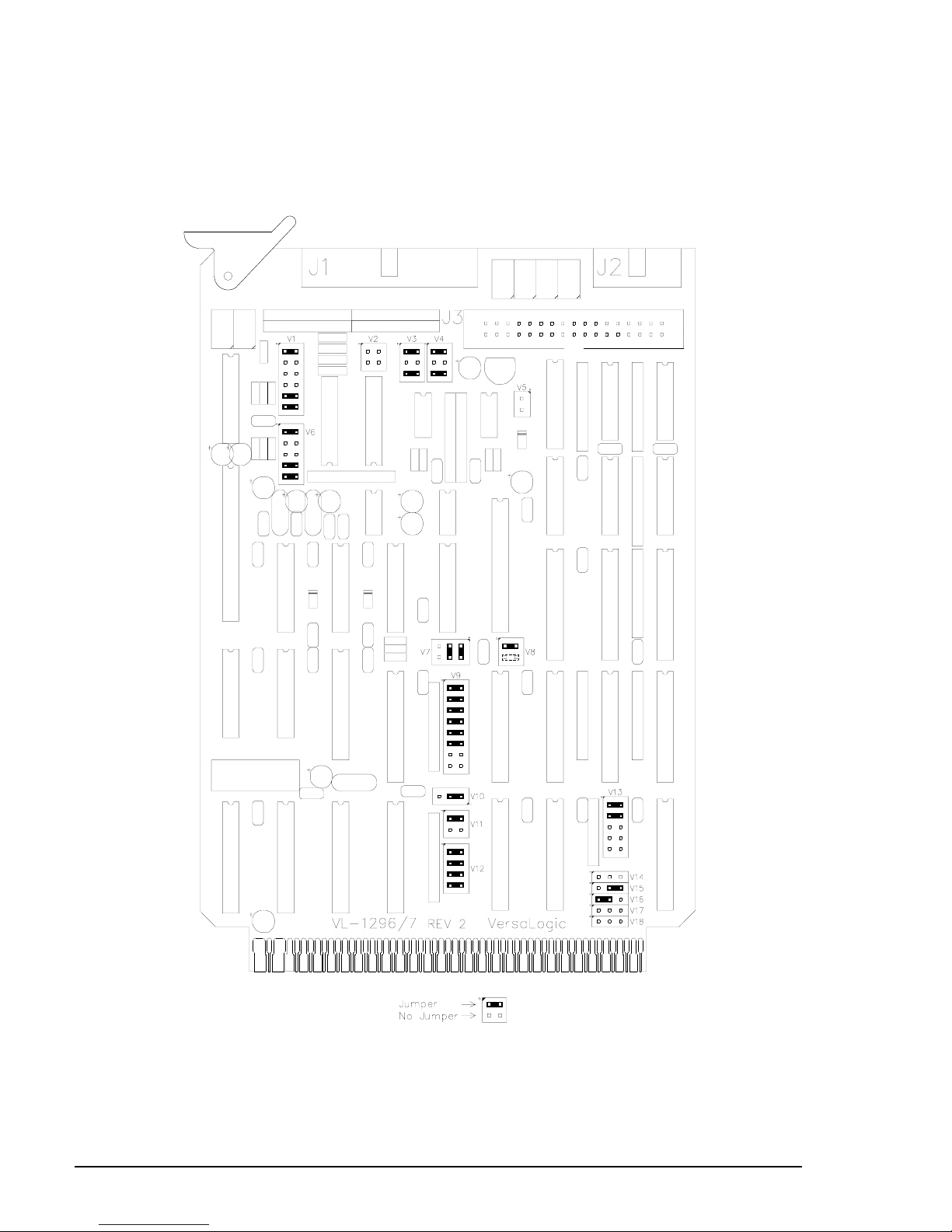
Figure 2-1 shows the jumper block locations on the VL-12CT96/7 card. The figures indicate the position
of the jumpers as shipped from the factory.
VL-12CT96/7 Analog & Digital I/O Card 2-1
Page 8
Configuration — Jumper Block Locations
VL-12CT96/7 Jumper Block Locations
Figure 2-1. Jumper Block Locations for VL-12CT96/7
2-2 VL-12CT96/7 Analog & Digital I/O Card
Page 9

Configuration — Jumper Options
VL-12CT96/7 Jumper Options
JumperJumper
Jumper
JumperJumper
BlockBlock
Block
BlockBlock
DescriptionDescription
Description
DescriptionDescription
V1[1-2] Input Mode . . . . . . . . . . . . . . . . . . . . . . . . . . . . . . . . . . . . . . . . . . . . . . . . . . . . . . . . . Single Ended 2-8
In –Single-Ended or Pseudo-Differential
Out – Differential
V1[3-4] Input Gain. . . . . . . . . . . . . . . . . . . . . . . . . . . . . . . . . . . . . . . . . . . . . . . . . . . . . . . . . . Normal 2-12
In – x100
Out – Normal
V1[5-6] Input Mode . . . . . . . . . . . . . . . . . . . . . . . . . . . . . . . . . . . . . . . . . . . . . . . . . . . . . . . . . Single Ended 2-8
In – Pseudo-Differential
Out – Single-Ended or Differential
V1[7-8] Input Mode . . . . . . . . . . . . . . . . . . . . . . . . . . . . . . . . . . . . . . . . . . . . . . . . . . . . . . . . . Single Ended 2-8
In – Differential
Out – Single-Ended or Pseudo-Differential
V1[9-10] Input Mode . . . . . . . . . . . . . . . . . . . . . . . . . . . . . . . . . . . . . . . . . . . . . . . . . . . . . . . . . Single Ended 2-8
In – Single-Ended
Out – Differential or Pseudo-Differential
V1[11-12] Differential Bias Resistor . . . . . . . . . . . . . . . . . . . . . . . . . . . . . . . . . . . . . . . . . . . . . . In Circuit 2-10
In –In Circuit
Out – Disconnected
V2[1-2] Analog Loopback (Channel 0) . . . . . . . . . . . . . . . . . . . . . . . . . . . . . . . . . . . . . . . . . . Independent 2-16
In –Connects DAC 0 output to ADC 0 input for diagnostic loopback
Out – Circuits operate independently
V2[3-4] Analog Loopback (Channel 1) . . . . . . . . . . . . . . . . . . . . . . . . . . . . . . . . . . . . . . . . . . Independent 2-16
In –Connects DAC 1 output to ADC 1 input for diagnostic loopback
Out – Circuits operate independently
V3[1-2] DAC Channel 0 Remote Sense (IR Drop Compensation) . . . . . . . . . . . . . . . . . . . . . Local sense 2-15
In –Local sense (no compensation)
Out – Remote sense
V3[3-4] Channel 0 Output Range (±5 Volt Selection) . . . . . . . . . . . . . . . . . . . . . . . . . . . . . . . ±10V 2-15
In –±5 Volts
Out – ±10 Volts
V3[5-6] Channel 0 Output Range (±10 Volt Selection) . . . . . . . . . . . . . . . . . . . . . . . . . . . . . . ±10V 2-15
In –±10 Volts
Out – ±5 Volts
V4[1-2] DAC Channel 1 Remote Sense (IR Drop Compensation) . . . . . . . . . . . . . . . . . . . . . Local Sense 2-15
In –Local sense (no compensation)
Out – Remote sense
V4[3-4] Channel 1 Output Range (±5 Volt Selection) . . . . . . . . . . . . . . . . . . . . . . . . . . . . . . . ±10V 2-15
In –±5 Volts
Out – ±10 Volts
V4[5-6] Channel 1 Output Range (±10 Volt Selection) . . . . . . . . . . . . . . . . . . . . . . . . . . . . . . ±10V 2-15
In –±10 Volts
Out – ±5 Volts
V5 Opto-22 I/O Rack Power . . . . . . . . . . . . . . . . . . . . . . . . . . . . . . . . . . . . . . . . . . . . . . External 2-17
In –I/O rack power provided locally
Out – I/O rack power provided externally
V6[1-8] Input Range . . . . . . . . . . . . . . . . . . . . . . . . . . . . . . . . . . . . . . . . . . . . . . . . . . . . . . . . ±10V 2-12
[1-2] & [7-8] In – ±10 Volts
[3-4] & [5-6] In – ±5 Volts
V6[9-10] Input Low Pass Filter . . . . . . . . . . . . . . . . . . . . . . . . . . . . . . . . . . . . . . . . . . . . . . . . . Enabled 2-13
In – Enabled
Out – Disabled
V7[1-2] Input Mode . . . . . . . . . . . . . . . . . . . . . . . . . . . . . . . . . . . . . . . . . . . . . . . . . . . . . . . . . Single Ended 2-8
In –Single-Ended or Pseudo-Differential
Out – Differential
V7[3-4] 5 µs Settling Delay . . . . . . . . . . . . . . . . . . . . . . . . . . . . . . . . . . . . . . . . . . . . . . . . . . . Enabled 2-13
In – Enabled
Out – Disabled
V7[5-6] 10 µs Settling Delay . . . . . . . . . . . . . . . . . . . . . . . . . . . . . . . . . . . . . . . . . . . . . . . . . . Disabled 2-13
In – Enabled
Out – Disabled
V8[1-2] Data Bus Width . . . . . . . . . . . . . . . . . . . . . . . . . . . . . . . . . . . . . . . . . . . . . . . . . . . . . 8-Bit 2-14
In –8-Bit Data Bus
Out – 16-Bit Data Bus
V8[3-4] Analog Input Resolution . . . . . . . . . . . . . . . . . . . . . . . . . . . . . . . . . . . . . . . . . . . . . . . Varies 2-14
In –16-Bit Resolution (VL-12CT97 only)
Out – 12-Bit Resolution (VL-12CT96 only)
AsAs
As
AsAs
ShippedShipped
Shipped
ShippedShipped
PagePage
Page
PagePage
VL-12CT96/7 Analog & Digital I/O Card 2-3
Page 10

Configuration — Jumper Options
JumperJumper
Jumper
JumperJumper
BlockBlock
Block
BlockBlock
DescriptionDescription
Description
DescriptionDescription
AsAs
As
AsAs
ShippedShipped
Shipped
ShippedShipped
PagePage
Page
PagePage
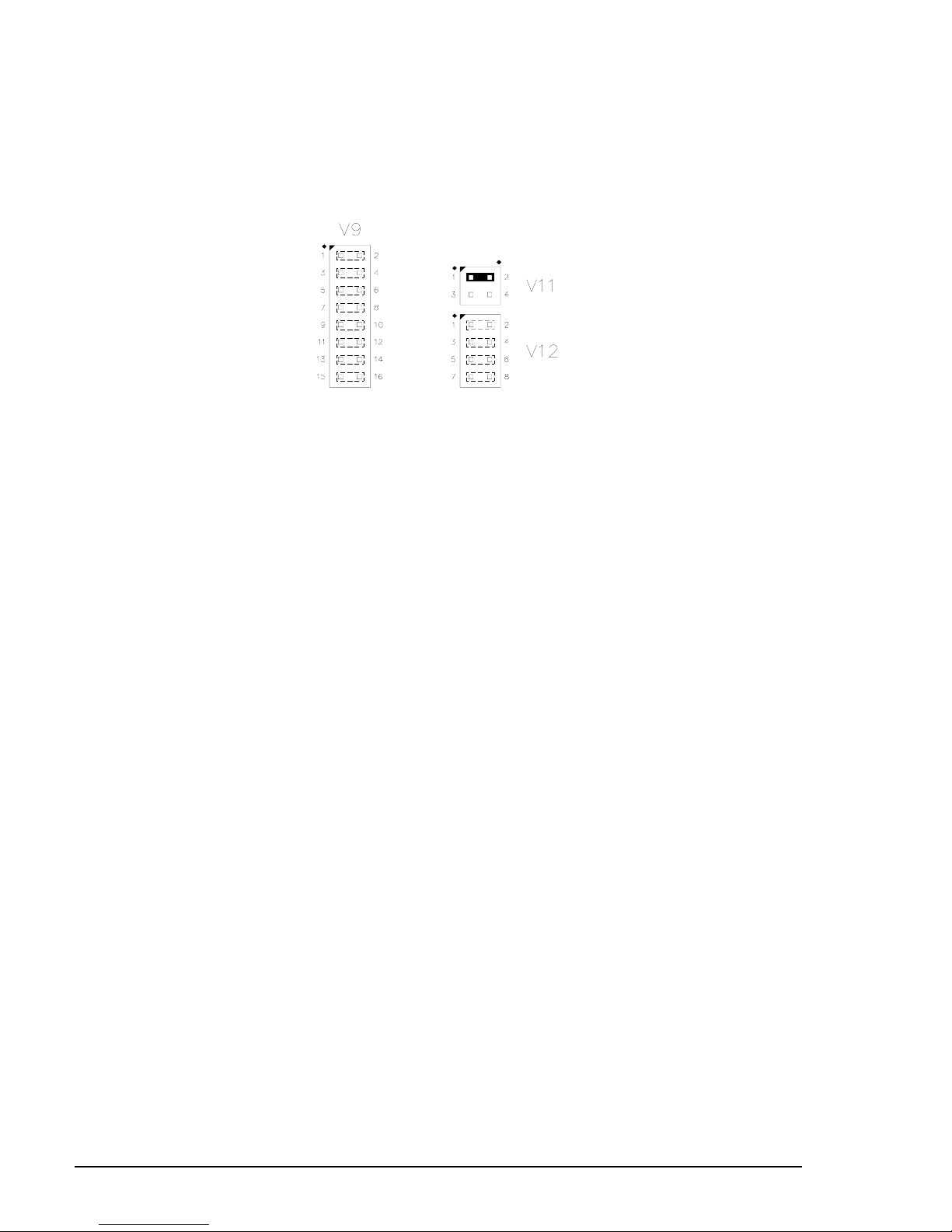
V9 Board Address (A8 – A15) . . . . . . . . . . . . . . . . . . . . . . . . . . . . . . . . . . . . . . . . . . . . . 0300H 2-6
[1-2] = In – A15 Decoded Low [1-2] = Out – A15 Decoded High
[3-4] = In – A14 Decoded Low [3-4] = Out – A14 Decoded High
[5-6] = In – A13 Decoded Low [5-6] = Out – A13 Decoded High
[7-8] = In – A12 Decoded Low [7-8] = Out – A12 Decoded High
[9-10] = In – A11 Decoded Low [9-10] = Out – A11 Decoded High
[11-12] = In – A10 Decoded Low [11-12] = Out – A10 Decoded High
[13-14] = In – A9 Decoded Low [13-14] = Out – A9 Decoded High
[15-16] = In – A8 Decoded Low [15-16] = Out – A8 Decoded High
V10 IOEXP Select. . . . . . . . . . . . . . . . . . . . . . . . . . . . . . . . . . . . . . . . . . . . . . . . . . . . . . . IOEXP Ignored 2-7
[1-2] = In – Board responds to IOEXP high and low (IOEXP ignored)
[2-3] = In – Board responds to IOEXP low
[Both] = Out – Board responds to IOEXP high
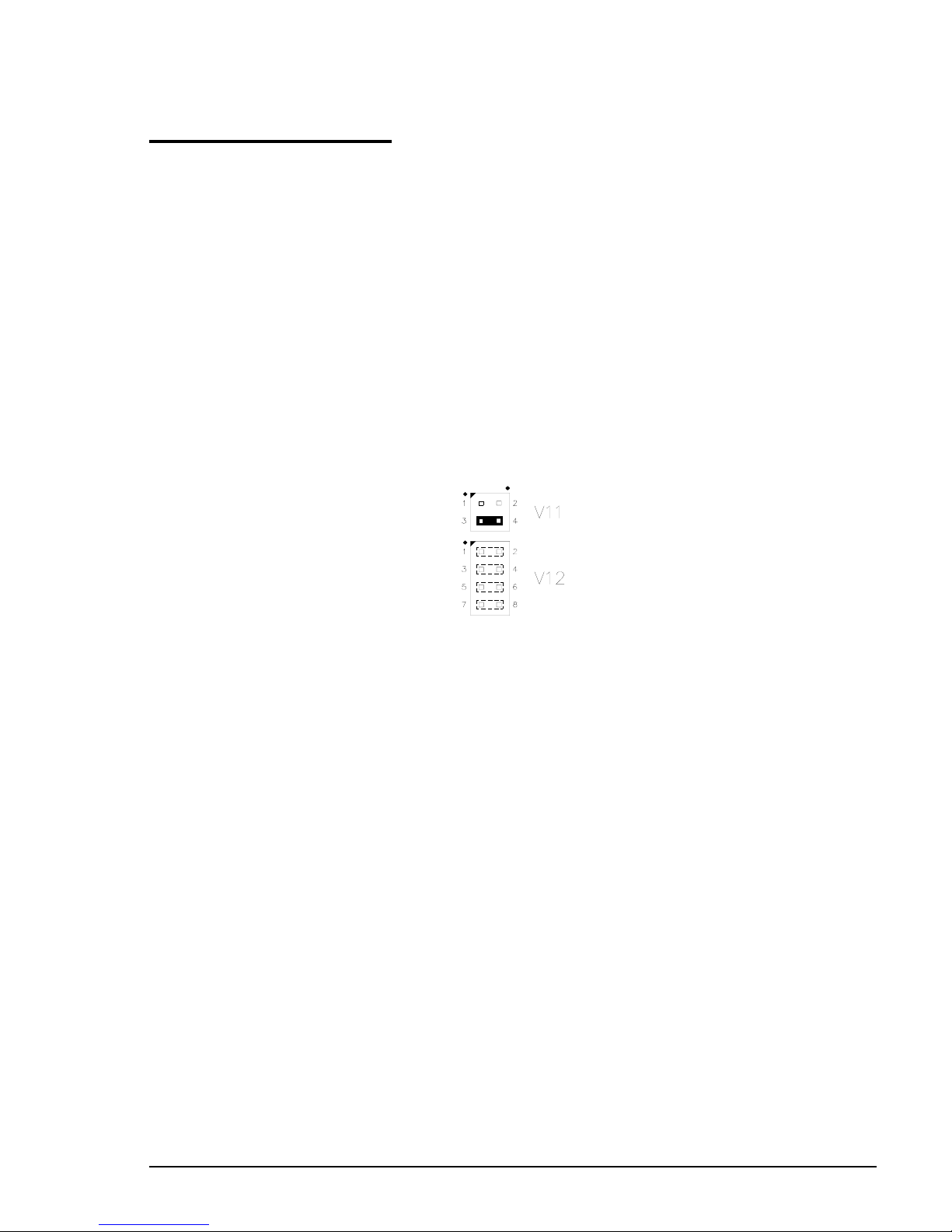
V11 Address Mode Selector . . . . . . . . . . . . . . . . . . . . . . . . . . . . . . . . . . . . . . . . . . . . . . . 16-Bit 2-5
[1-2] = In – 16-Bit Address Decoding
[3-4] = In – 8-Bit Address Decoding
V12 Board Address (A4 – A7) . . . . . . . . . . . . . . . . . . . . . . . . . . . . . . . . . . . . . . . . . . . . . . 0300H 2-5
[1-2] = In – A7 Decoded Low [1-2] = Out – A7 Decoded High
[3-4] = In – A6 Decoded Low [3-4] = Out – A6 Decoded High
[5-6] = In – A5 Decoded Low [5-6] = Out – A5 Decoded High
[7-8] = In – A4 Decoded Low [7-8] = Out – A4 Decoded High
V13[1-2] Parallel Port Interrupt Edge Selector . . . . . . . . . . . . . . . . . . . . . . . . . . . . . . . . . . . . . Rising Edge Only 2-18
In –Rising Edge Only
Out – Rising and Falling Edges
V13[3-4] Parallel Port Interrupt Select (Module 0). . . . . . . . . . . . . . . . . . . . . . . . . . . . . . . . . . . Enabled 2-18
In –Activity on Module 0 (J3 Pin 31) generates interrupt request
Out – Disabled
V13[5-6] Parallel Port Interrupt Select (Module 1). . . . . . . . . . . . . . . . . . . . . . . . . . . . . . . . . . . Disabled 2-18
In –Activity on Module 1 (J3 Pin 29) generates interrupt request
Out – Disabled
V13[7-8] Parallel Port Interrupt Select (Module 2). . . . . . . . . . . . . . . . . . . . . . . . . . . . . . . . . . . Disabled 2-18
In –Activity on Module 2 (J3 Pin 27) generates interrupt request
Out – Disabled
V13[9-10] Parallel Port Interrupt Select (Module 3). . . . . . . . . . . . . . . . . . . . . . . . . . . . . . . . . . . Disabled 2-18
In –Activity on Module 3 (J3 Pin 25) generates interrupt request
Out – Disabled
V14[1-2] Use STD Bus IRQx to carry parallel port interrupt signal . . . . . . . . . . . . . . . . . . . . . . Disabled 2-19
In –Connects parallel port interrupt circuitry to STD Bus IRQx (E47)
Out – Frees IRQx to be used for other purposes
V14[2-3] Use STD Bus IRQx to carry ADC conversion complete interrupt. . . . . . . . . . . . . . . . Disabled 2-19
In –Connects ADC interrupt circuitry to STD Bus IRQx (E47)
Out – Frees IRQx to be used for other purposes
V15[1-2] Use STD Bus IRQ* to carry parallel port interrupt signal . . . . . . . . . . . . . . . . . . . . . . Disabled 2-19
In –Connects parallel port interrupt circuitry to STD Bus IRQ* (P44)
Out – Frees IRQ* to be used for other purposes
V15[2-3] Use STD Bus IRQ* to carry ADC conversion complete interrupt . . . . . . . . . . . . . . . . Enabled 2-19
In –Connects ADC interrupt circuitry to STD Bus IRQ* (P44)
Out – Frees IRQ* to be used for other purposes
V16[1-2] Use STD Bus IRQ1* to carry parallel port interrupt signal . . . . . . . . . . . . . . . . . . . . . Enabled 2-19
In –Connects parallel port interrupt circuitry to STD Bus IRQ1* (P37)
Out – Frees IRQ1* to be used for other purposes
V16[2-3] Use STD Bus IRQ1* to carry ADC conversion complete interrupt . . . . . . . . . . . . . . . Disabled 2-19
In –Connects ADC interrupt circuitry to STD Bus IRQ1* (P37)
Out – Frees IRQ1* to be used for other purposes
V17[1-2] Use STD Bus IRQ2* to carry parallel port interrupt signal . . . . . . . . . . . . . . . . . . . . . Disabled 2-19
In –Connects parallel port interrupt circuitry to STD Bus IRQ2* (P50)
Out – Frees IRQ2* to be used for other purposes
V17[2-3] Use STD Bus IRQ2* to carry ADC conversion complete interrupt . . . . . . . . . . . . . . . Disabled 2-19
In –Connects ADC interrupt circuitry to STD Bus IRQ2* (P50)
Out – Frees IRQ2* to be used for other purposes
V18[1-2] Use STD Bus IRQ3* to carry parallel port interrupt signal . . . . . . . . . . . . . . . . . . . . . Disabled 2-19
In –Connects parallel port interrupt circuitry to STD Bus IRQ3* (E67)
Out – Frees IRQ3* to be used for other purposes
V18[2-3] Use STD Bus IRQ3* to carry ADC conversion complete interrupt . . . . . . . . . . . . . . . Disabled 2-19
In –Connects ADC interrupt circuitry to STD Bus IRQ3* (E67)
Out – Frees IRQ3* to be used for other purposes
Figure 2-2. VL-12CT96/7 Jumper Functions
2-4 VL-12CT96/7 Analog & Digital I/O Card
Page 11
Configuration — Board Addressing
Board Addressing
The VL-12CT96/7 card supports both 8- and 16-bit I/O addressing. 8-bit addressing is used with most
8-bit processors (Z80, 8085, 6809, etc.) which provide 256 I/O addresses. 16-bit addressing can be used
with 16-bit processors (i.e. 8088, 80188, etc.) to decode up to 65536 I/O port addresses.
Both 8- and 16-bit addressing can be extended (capacity doubled) using the IOEXP signal which is
decoded on board.
As shipped, the board is configured for 16-bit addressing with a board address of hex 0300. The card
occupies sixteen consecutive I/O addresses (0300H to 030FH). Twelve of these addresses are mapped
to control, data, and status registers, the remaining four are inaccessible. See the I/O Port Mapping
section on page 4-1 for further information.
8-Bit Addressing
To configure the board for an 8-bit I/O address, refer to the figure below. Use the table to select the
jumpering for the appropriate upper hex digit of the desired starting address (i.e., “3” and “0” = hex
address 30). Note: the lower digit is always “0.”
V12 V12 V12 V12 Upper Lower
1-2 3-4 5-6 7-8 Digit Digit
XXXX0 Always “0”
XXX—1
XX—X2
XX——3
X—XX 4
X—X—5
X——X 6
X——— 7
—XXX8
—XX—9
—X—XA
—X——B
——X X C
——X—D
———X E
————F
X = Jumper installed
—= Jumper removed
JumperJumper
Jumper
JumperJumper
BlockBlock
Block
BlockBlock
V12 Board Address (A4 – A7) . . . . . . . . . . . . . . . . . . . . . . . . . . . . . . . . . . . . . . . . . . . . . . . . . . 0300H (16-Bit)
DescriptionDescription
Description
DescriptionDescription
[1-2] = In – A7 Decoded Low [1-2] = Out – A7 Decoded High
[3-4] = In – A6 Decoded Low [3-4] = Out – A6 Decoded High
[5-6] = In – A5 Decoded Low [5-6] = Out – A5 Decoded High
[7-8] = In – A4 Decoded Low [7-8] = Out – A4 Decoded High
AsAs
As
AsAs
ShippedShipped
Shipped
ShippedShipped
VL-12CT96/7 Analog & Digital I/O Card 2-5
Figure 2-3. 8-Bit Address Jumpers
Page 12
Configuration — Board Addressing
16-Bit Addressing
To configure the board for a 16-bit I/O address refer to the figure below. Use the table to select the
jumpering for the appropriate four hex digits of the desired starting address (i.e., “1” and “2” and “3”
and “0” = hex address 1230). Note: the lower digit is always “0.”
V9 V9 V9 V9 Upper V9 V9 V9 V9 2nd V12 V12 V12 V12 3rd Lower
1-2 3-4 5-6 7-8 Digit 9-10 11-12 13-14 15-16 Digit 1-2 3-4 5-6 7-8 Digit Digit
XXXX0 XXXX0 XXXX0 Always “0”
XXX—1 XXX—1 XXX—1
XX—X2 XX—X2 XX—X2
XX——3 XX——3 XX——3
X—XX 4 X—X X 4 X—XX 4
X—X—5 X—X—5 X—X—5
X——X 6 X——X6 X——X 6
X——— 7 X———7 X——— 7
—XXX8 —XXX8 —XXX8
—XX—9 —XX—9 —XX—9
—X—XA —X—X A —X—XA
—X——B —X——B —X——B
——X X C ——X X C ——X X C
——X—D ——X—D ——X—D
———X E ———X E ———X E
————F ———— F ————F
X = Jumper installed
-- = Jumper removed
JumperJumper
Jumper
JumperJumper
BlockBlock
Block
BlockBlock
V9 Board Address (A8 – A15) . . . . . . . . . . . . . . . . . . . . . . . . . . . . . . . . . . . . . . . . . . . . . . . . . 0300H
V12 Board Address (A4 – A7) . . . . . . . . . . . . . . . . . . . . . . . . . . . . . . . . . . . . . . . . . . . . . . . . . . 0300H
DescriptionDescription
Description
DescriptionDescription
[1-2] = In – A15 Decoded Low [1-2] = Out – A15 Decoded High
[3-4] = In – A14 Decoded Low [3-4] = Out – A14 Decoded High
[5-6] = In – A13 Decoded Low [5-6] = Out – A13 Decoded High
[7-8] = In – A12 Decoded Low [7-8] = Out – A12 Decoded High
[9-10] = In – A11 Decoded Low [9-10] = Out – A11 Decoded High
[11-12] = In – A10 Decoded Low [11-12] = Out – A10 Decoded High
[13-14] = In – A9 Decoded Low [13-14] = Out – A9 Decoded High
[15-16] = In – A8 Decoded Low [15-16] = Out – A8 Decoded High
[1-2] = In – A7 Decoded Low [1-2] = Out – A7 Decoded High
[3-4] = In – A6 Decoded Low [3-4] = Out – A6 Decoded High
[5-6] = In – A5 Decoded Low [5-6] = Out – A5 Decoded High
[7-8] = In – A4 Decoded Low [7-8] = Out – A4 Decoded High
Figure 2-4. 16-Bit Address Jumpers
AsAs
As
AsAs
ShippedShipped
Shipped
ShippedShipped
2-6 VL-12CT96/7 Analog & Digital I/O Card
Page 13

Configuration — Board Addressing/Data Bus Width
IOEXP Signal
The IOEXP (I/O expansion) signal on the STD Bus is normally used to select between two different I/
O banks or maps. It can be used to double the number of available I/O addresses in the system (by
selecting between two banks of I/O boards). The IOEXP signal is usually controlled by (or jumpered
to ground on) the system CPU card.
A low IOEXP signal usually selects the standard or normal I/O map. A high IOEXP signal usually
selects the secondary or alternate I/O map. Boards that ignore (or do not decode) IOEXP will appear
in both I/O maps.
As shipped the IOEXP jumper is configured to ignore the IOEXP signal. The board will be addressed
whether the IOEXP signal is high or low. It can be jumpered for two other modes as shown below.
JumperJumper
Jumper
JumperJumper
BlockBlock
Block
BlockBlock
V10 IOEXP Select . . . . . . . . . . . . . . . . . . . . . . . . . . . . . . . . . . . . . . . . . . . . . . . . . . . . . . . . . . . IOEXP Ignored
DescriptionDescription
Description
DescriptionDescription
[1-2] = In – Board responds to IOEXP high and low (IOEXP ignored)
[2-3] = In – Board responds to IOEXP low
[Both] = Out – Board responds to IOEXP high
AsAs
As
AsAs
ShippedShipped
Shipped
ShippedShipped
Figure 2-5. IOEXP Options
Data Bus Width
The VL-12CT96/7 provides both 8-bit and 16-bit data paths to the bus. The 8-bit mode is compatible
with STD 80, STD Z80, and STD 32 bus specifications. The 16-bit mode is used only when operating
the card in an STD 32 card cage.
In 8-bit mode, the register map for the VL-12CT96/7 is a superset of the Analog Devices RTI-1265 board.
In 16-bit mode, the registers are remapped to even addresses for efficient I/O access. This allows the
full A/D data word to be read in a single bus cycle. See the I/O Port Mapping section on page 4-1 for
further information.
JumperJumper
Jumper
JumperJumper
BlockBlock
Block
BlockBlock
V8[1-2] Data Bus Width. . . . . . . . . . . . . . . . . . . . . . . . . . . . . . . . . . . . . . . . . . . . . . . . . . . . . . . . . . 8-Bit
DescriptionDescription
Description
DescriptionDescription
In – 8-Bit Data Bus
Out – 16-Bit Data Bus
VL-12CT96/7 Analog & Digital I/O Card 2-7
Figure 2-14. Data Bus Width Jumper
AsAs
As
AsAs
ShippedShipped
Shipped
ShippedShipped
Page 14
Configuration — Analog Input
Analog Input Configuration
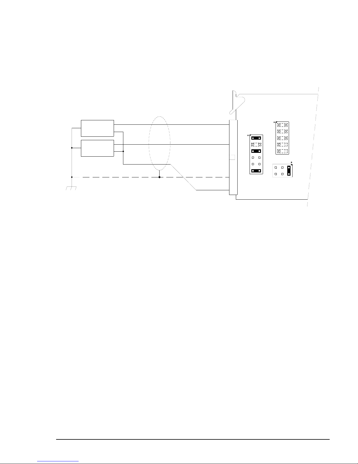
The VL-12CT96/7 board accommodates 16 single-ended or 8 differential input channels.
Input Mode
The board can be configured for three types of analog inputs: differential, single-ended, or pseudodifferential. All inputs connected to the board must be of the same type.
When operated in differential mode, four channels can be configured to accept 4-20ma current loop
input.
Typical connections for the three input modes are shown in the figures below. Since ground loops
(current flowing between various equipment ground lines) affect analog measurements made with
reference to ground, careful attention should be paid to the ground connections shown. In particular,
the STD Bus power supply logic ground line should never be connected to earth ground when operating
in the differential or pseudo-differential modes.
Single Ended Mode
Single-ended mode is used for signals that are referenced to a common ground. It is normally used only
for higher level signals on short distance runs (less than 10 feet). 16 input channels are available in
single-ended mode.
OPTIONAL
V0
V1
VL-12CT96
VL-12CT97
+
-
+
-
CHANNEL 0
CHANNEL 1
AGND
1
V1
1
3
5
5
7
9
9
11
As Shipped
V6
1
3
5
2
7
4
9
6
8
10
12
2
4
6
8
10
5
3
1
V7
2
4
6
Figure 2-6. Single Ended Input Mode
2-8 VL-12CT96/7 Analog & Digital I/O Card
Page 15
Configuration — Analog Input
Pseudo-Differential Mode
Pseudo-differential mode is used for signals that are not referenced to ground, but are all connected
to a single common return line. This mode can provide most of the advantages of full differential input
while requiring fewer total wires. 16 input channels are available in pseudo-differential mode. This
mode is used when connecting to a 5B01 signal conditioning rack.
VL-12CT96
VL-12CT97
OPTIONAL
V0
V1
+
CHANNEL 0
-
+
CHANNEL 1
-
AGND
P.D. SENSE
Figure 2-7. Pseudo-Differential Input Mode
25
V6
1
V1
1
3
5
5
7
9
11
1
3
5
7
4
9
6
8
10
12
9
2
4
62
8
10
5
3
1
V7
2
4
6
VL-12CT96/7 Analog & Digital I/O Card 2-9
Page 16
Configuration — Analog Input
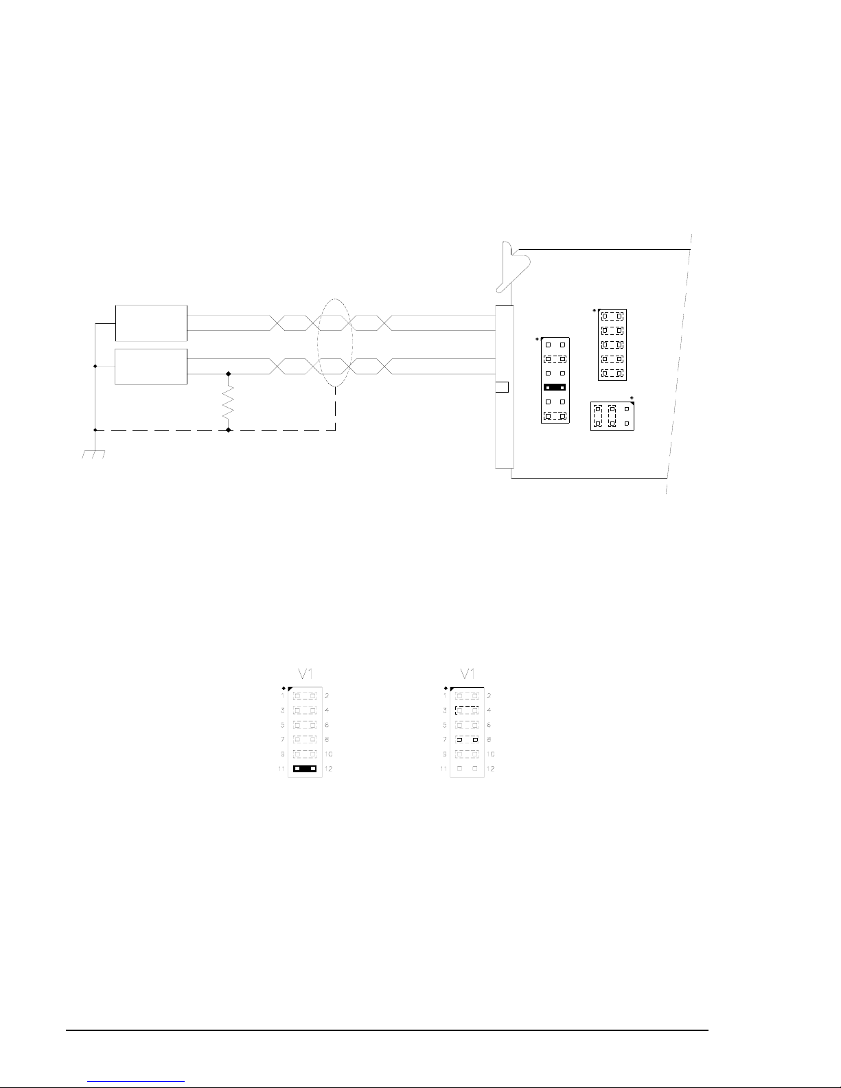
Differential Mode
Differential mode is used for signals that are not referenced to a common ground point. Each input
signal is represented as a voltage difference between two signal conductors (usually twisted wires), and
is presented to the board as a (+) and (–) pair. Differential mode reduces the effects of electromagnetically induced noise and ground currents in electrically noisy environments. It is especially useful in
eliminating the effects of common mode noise generated on input lines over longer distances. Eight
input channels are available in differential mode.
VL-12CT96
VL-12CT97
V6
1
2
3
4
5
2
4
6
8
10
12
6
7
8
9
10
5
3
1
V7
2
4
6
OPTIONAL
V0
V1
+
-
CHANNEL 0
+
-
SEE
TEXT
CHANNEL 1
+
1
-
2
+
5
-
4
V1
1
3
5
7
9
11
Figure 2-8. Differential Input Mode
Note that in full differential operation a return path must be provided for the bias currents of the input
amplifier. An on-board 1M Ω resistor is provided for this purpose. Jumper V1[11-12] should be
inserted.
In noisy electrical environments, the bias resistor should be located in close proximity to the voltage
source. Jumper V1[11-12] should be removed under these conditions.
JumperJumper
Jumper
JumperJumper
BlockBlock
Block
BlockBlock
DescriptionDescription
Description
DescriptionDescription
V1[11-12] Differential Bias Resistor. . . . . . . . . . . . . . . . . . . . . . . . . . . . . . . . . . . . . . . . . . . . . . . . In Circuit
In – In Circuit
Out – Disconnected
AsAs
As
AsAs
ShippedShipped
Shipped
ShippedShipped
Figure 2-9. Bias Resistor
2-10 VL-12CT96/7 Analog & Digital I/O Card
Page 17
Configuration — Analog Input
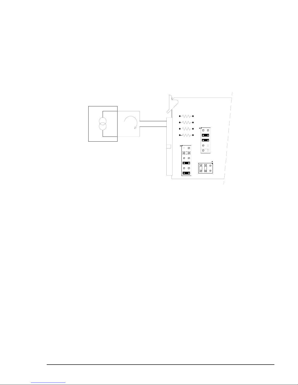
Current Loop Mode
In addition to voltage mode inputs, the VL-12CT96/7 can accept up to four 4-20 ma current loop inputs.
Channels 0 through 3 can be converted to current-loop input by installing 200 to 250 Ω, ¼W, 0.1%
precision resistors in locations R4 through R7 respectively.
The board must be jumpered for differential mode, and the input range should be jumpered for ±5V
operation when using current loop inputs. A signal proportional to the 4-20 ma current is developed
across the precision resistors. This voltage is applied to the VL-12CT96/7 as a differential-mode signal,
and is converted into digital values.
VL-12CT96
+
I
LOOP
CHANNEL 0
1
2
-
VL-12CT97
R4
R5
R6
R7
V1
1
3
5
7
9
11
V6
1
2
3
4
5
6
7
2
4
6
8
10
12
8
9
10
5
3
1
V7
2
4
6
Figure 2-10. Current Loop Input Mode
VL-12CT96/7 Analog & Digital I/O Card 2-11
Page 18
Configuration — Analog Input
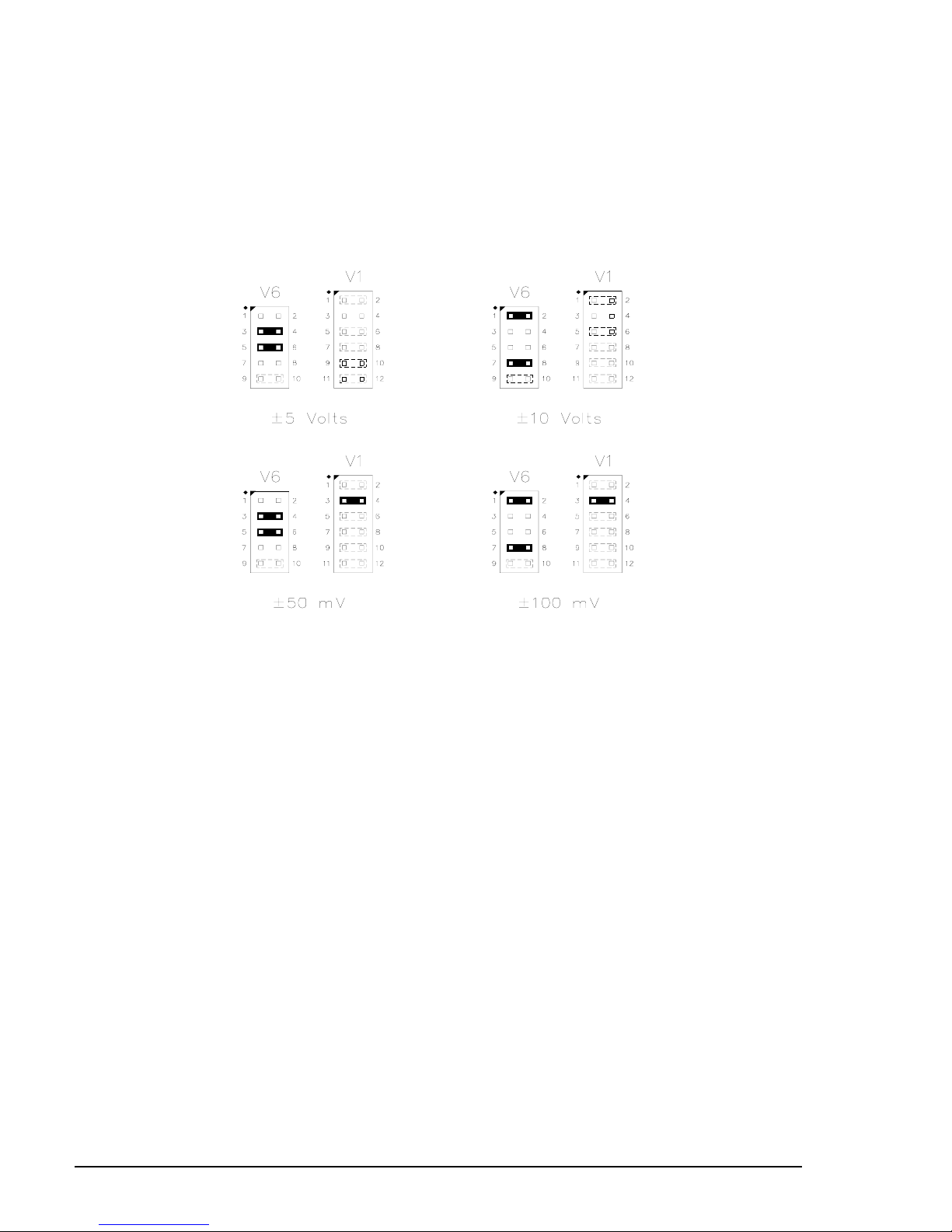
Input Range
The board may be operated with an input range of ±5 volts, ±10 volts, ±50 mv, or ±100 mv. To achieve
the maximum digital resolution and to prevent saturation, the range which most closely matches the
input signal should be chosen. All channels operate with the same input range.
As shipped the board is configured for ±10 volt operation. It can be jumpered for other ranges as shown
below.
JumperJumper
Jumper
JumperJumper
BlockBlock
Block
BlockBlock
V1[3-4] Input Gain . . . . . . . . . . . . . . . . . . . . . . . . . . . . . . . . . . . . . . . . . . . . . . . . . . . . . . . . . . . . . . Normal
V6[1-8] Input Range . . . . . . . . . . . . . . . . . . . . . . . . . . . . . . . . . . . . . . . . . . . . . . . . . . . . . . . . . . . . ±10V
DescriptionDescription
Description
DescriptionDescription
In – x100
Out – Normal
[1-2] & [7-8] In – ±10 Volts
[3-4] & [5-6] In – ±5 Volts
AsAs
As
AsAs
ShippedShipped
Shipped
ShippedShipped
Figure 2-11. Input Range Jumper
2-12 VL-12CT96/7 Analog & Digital I/O Card
Page 19
Configuration — Analog Input
Settling Time
The VL-12CT96/7 board inserts a short delay between the time a channel is selected and time the A/
D conversion begins. The delay allows the multiplexer and associated circuitry to properly settle for
a more accurate reading.
The settling delay starts when the Channel Select register is written to by software, or when the Data
High register is read (in auto increment mode). After channel selection (during the settling time), the
A/D conversion cycle can be started by writing to the Convert register; however, the A/D converter is
not triggered until the delay time elapses. The time delay is not inserted when one channel is read
repeatedly.
The standard 5 µS delay (as shipped) is used for ±5V or ±10V input ranges. The longer 10 µS settling
delay is needed for the ±50 mv or ±100 mv input ranges.
Settling delay times can be selected as indicated in the figure below.
JumperJumper
Jumper
JumperJumper
BlockBlock
Block
BlockBlock
V7[3-4] 5 µS Settling Delay . . . . . . . . . . . . . . . . . . . . . . . . . . . . . . . . . . . . . . . . . . . . . . . . . . . . . . . Enabled
V7[5-6] 10 µS Settling Delay . . . . . . . . . . . . . . . . . . . . . . . . . . . . . . . . . . . . . . . . . . . . . . . . . . . . . . Disabled
DescriptionDescription
Description
DescriptionDescription
In – Enabled
Out – Disabled
In – Enabled
Out – Disabled
AsAs
As
AsAs
ShippedShipped
Shipped
ShippedShipped
Figure 2-12. Settling Time Jumpers
Low Pass Filter
A 1 MHz low pass filter between the instrumentation amplifier and the A/D convertor can be selected
as shown in the figure below. This filter is used to reject high frequency noise and is normally enabled.
JumperJumper
Jumper
JumperJumper
BlockBlock
Block
BlockBlock
DescriptionDescription
Description
DescriptionDescription
AsAs
As
AsAs
ShippedShipped
Shipped
ShippedShipped
V6[9-10] Input Low Pass Filter . . . . . . . . . . . . . . . . . . . . . . . . . . . . . . . . . . . . . . . . . . . . . . . . . . . . . Enabled
In – Enabled
Out – Disabled
VL-12CT96/7 Analog & Digital I/O Card 2-13
Figure 2-13. Low Pass Filter Jumper
Page 20

Configuration — Analog Input
Input Resolution
The VL-12CT96 provides 12 bits of resolution (4096 digital counts). For correct operation, jumper V8[34] should be removed. The VL-12CT97 provides 16 bits of resolution (65536 counts) for applications
which require finer resolution. For correct operation, jumper V8[3-4] should be inserted.
JumperJumper
Jumper
JumperJumper
BlockBlock
Block
BlockBlock
V8[3-4] Analog Input Resolution . . . . . . . . . . . . . . . . . . . . . . . . . . . . . . . . . . . . . . . . . . . . . . . . . . . Varies
DescriptionDescription
Description
DescriptionDescription
In – 16-Bit Resolution (VL-12CT97 only)
Out – 12-Bit Resolution (VL-12CT96 only)
AsAs
As
AsAs
ShippedShipped
Shipped
ShippedShipped
Figure 2-15. Input Range Selection
Analog Output Configuration
The VL-12CT96/7 board accommodates two analog output channels. Both output channels are singleended and are referenced to analog ground. The digital data format is two’s complement.
2-14 VL-12CT96/7 Analog & Digital I/O Card
Page 21
Configuration — Analog Output
Output V oltage Range
Each output channel can be configured independently to produce output voltage ranges of ±5 volts, or
±10 volts as shown below.
JumperJumper
Jumper
JumperJumper
BlockBlock
Block
BlockBlock
V3[3-4] Channel 0 Output Range (±5 Volt Selection) . . . . . . . . . . . . . . . . . . . . . . . . . . . . . . . . . . . ±10V
V3[5-6] Channel 0 Output Range (±10 Volt Selection) . . . . . . . . . . . . . . . . . . . . . . . . . . . . . . . . . . ±10V
V4[3-4] Channel 1 Output Range (±5 Volt Selection) . . . . . . . . . . . . . . . . . . . . . . . . . . . . . . . . . . . ±10V
V4[5-6] Channel 1 Output Range (±10 Volt Selection) . . . . . . . . . . . . . . . . . . . . . . . . . . . . . . . . . . ±10V
DescriptionDescription
Description
DescriptionDescription
In – ±5 Volts
Out – ±10 Volts
In – ±10 Volts
Out – ±5 Volts
In – ±5 Volts
Out – ±10 Volts
In – ±10 Volts
Out – ±5 Volts
AsAs
As
AsAs
ShippedShipped
Shipped
ShippedShipped
Figure 2-16. Output Voltage Range
Output Local/Remote Sense
When a load is driven over a long cable, the resistance of the wire can cause a voltage drop to occur. This
can result in erroneous signal levels at the remote end of the line. The VL-12CT96/7 board can compensate
for this drop (up to 3 volts of loss) by measuring the voltage at the far end of the line through a separate
sense line.
Each channel can be jumpered for local sense (voltage measured at the card edge, no sense wire used),
or remote sense (voltage measured at the destination, sense wire required).
JumperJumper
Jumper
JumperJumper
BlockBlock
Block
BlockBlock
V3[1-2] DAC Channel 0 Remote Sense (IR Drop Compensation). . . . . . . . . . . . . . . . . . . . . . . . . . Local sense
V4[1-2] DAC Channel 1 Remote Sense (IR Drop Compensation). . . . . . . . . . . . . . . . . . . . . . . . . . Local sense
DescriptionDescription
Description
DescriptionDescription
In – Local sense (no compensation)
Out – Remote sense
In – Local sense (no compensation)
Out – Remote sense
VL-12CT96/7 Analog & Digital I/O Card 2-15
Figure 2-17. Remote Sense Jumpers
AsAs
As
AsAs
ShippedShipped
Shipped
ShippedShipped
Page 22
Configuration — Analog Output
Output Current Loop Option
Channel 0 can optionally be configured to produce current loop output in the range of 4 to 20 mA.
Normally this is a factory installed option. Contact VersaLogic for further information.
Note: When using the 4-20 mA option, channel 0 must be configured for ±10 volt output range.
An external loop power source between 15 and 30 volts must be connected to J1 pin 5 (LP0) as shown
below. This power source must be capable of providing 25 mA of current.
VL-12CT96
VL-12CT97
CHANNEL 0
0 to +10V
J2
5
~
5
~
mA
4 to 20 mA
6
4
R
LOAD
EXTERNAL LOOP
POWER SOURCE
+15V TO +30V
Figure 2-18. Current Loop Connection
Output Voltage Loopback
The output channels can be connected to their corresponding input channels for a direct readback of
the voltage. The looped back output channels are also available on J1 for user and 5B01 rack
connections.
JumperJumper
Jumper
JumperJumper
BlockBlock
Block
BlockBlock
V2[1-2] Analog Loopback (Channel 0) . . . . . . . . . . . . . . . . . . . . . . . . . . . . . . . . . . . . . . . . . . . . . . Independent
V2[3-4] Analog Loopback (Channel 1) . . . . . . . . . . . . . . . . . . . . . . . . . . . . . . . . . . . . . . . . . . . . . . Independent
DescriptionDescription
Description
DescriptionDescription
In – Connects DAC 0 output to ADC 0 input for diagnostic loopback
Out – Circuits operate independently
In – Connects DAC 1 output to ADC 1 input for diagnostic loopback
Out – Circuits operate independently
Figure 2-19. Analog Output Loopback
2-16 VL-12CT96/7 Analog & Digital I/O Card
AsAs
As
AsAs
ShippedShipped
Shipped
ShippedShipped
Page 23

Configuration — 5B01 Rack/Digital Input/Output
5B01 Analog Signal Conditioning Rack
When using a 5B01 series analog signal conditioning rack connected to J1, the input mode should be
set to Pseudo-Differential mode and the input range should be set to ±5V. The output channels can
be connected to the 5B01 rack using the Output Voltage Loopback jumpers, and should be configured
for ±5V output.
Digital Input/Output Configuration
This card has 16 digital I/O lines that can be independantly programmed as inputs or outputs. The
I/O connector is compatible with 8 and 16 position modular I/O racks.
Rack P ower Contr ol
The VL-12CT96/7 board includes provisions for powering the external I/O rack assembly with +5 volts
at 500 ma.
When jumper V5 is installed, the I/O rack power line (I/O rack pin 49) is connected directly to +5 volts
on the STD Bus. If the I/O rack is powered by a separate external supply, either a jumper from the
I/O rack or the V5 jumper must be removed.
Note that the +5 volt power output from the VL-12CT96/7 card can be shorted to ground if the connector
is not correctly oriented at either end of the interface cable. The use of keys in the connectors, or very
clear markings on the connectors, is recommended to prevent backwards connection of the cable.
JumperJumper
Jumper
JumperJumper
BlockBlock
Block
BlockBlock
V5 Opto-22 I/O Rack Power . . . . . . . . . . . . . . . . . . . . . . . . . . . . . . . . . . . . . . . . . . . . . . . . . . External
DescriptionDescription
Description
DescriptionDescription
In – I/O rack power provided by VL-12CT96/7
Out – I/O rack power provided externally
AsAs
As
AsAs
ShippedShipped
Shipped
ShippedShipped
Figure 2-20. Rack Power Control Jumper
VL-12CT96/7 Analog & Digital I/O Card 2-17
Page 24

Configuration — Digital Input/Output
Digital I/O Interrupts
Up to four parallel port signals can be selected by jumper V13 to trigger an interrupt request when the
logic state on these signals changes state.
JumperJumper
Jumper
JumperJumper
BlockBlock
Block
BlockBlock
V13[3-4] Parallel Port Interrupt Select (Module 0) . . . . . . . . . . . . . . . . . . . . . . . . . . . . . . . . . . . . . . . Enabled
V13[5-6] Parallel Port Interrupt Select (Module 1) . . . . . . . . . . . . . . . . . . . . . . . . . . . . . . . . . . . . . . . Disabled
V13[7-8] Parallel Port Interrupt Select (Module 2) . . . . . . . . . . . . . . . . . . . . . . . . . . . . . . . . . . . . . . . Disabled
V13[9-10] Parallel Port Interrupt Select (Module 3) . . . . . . . . . . . . . . . . . . . . . . . . . . . . . . . . . . . . . . . Disabled
DescriptionDescription
Description
DescriptionDescription
In – Activity on Module 0 (J3 Pin 31) generates interrupt request
Out – Disabled
In – Activity on Module 1 (J3 Pin 29) generates interrupt request
Out – Disabled
In – Activity on Module 2 (J3 Pin 27) generates interrupt request
Out – Disabled
In – Activity on Module 3 (J3 Pin 25) generates interrupt request
Out – Disabled
AsAs
As
AsAs
ShippedShipped
Shipped
ShippedShipped
Figure 2-21. Digital Interrupts
Edge Selection
Two edge options are available: single edge, and double edge mode. Single edge mode generates an
interrupt when any of the selected input signals (at connector J3) switches from high-to-low. Double
edge mode generates an interrupt on both high-to-low and low-to-high transitions.
JumperJumper
Jumper
JumperJumper
BlockBlock
Block
BlockBlock
V13[1-2] Inte rr u pt Edge Selector . . . . . . . . . . . . . . . . . . . . . . . . . . . . . . . . . . . . . . . . . . . . . . . . . . . . Rising Edge Only
DescriptionDescription
Description
DescriptionDescription
In – Rising Edge Only
Out – Rising and Falling Edges
Figure 2-22. Digital Interrupt Edge Select
2-18 VL-12CT96/7 Analog & Digital I/O Card
AsAs
As
AsAs
ShippedShipped
Shipped
ShippedShipped
Page 25

Configuration — Interrupt
Interrupt Configuration
Jumpers V14 through V18 connect the interrupt request signals from the VL-12CT96/7 card to five
STD Bus interrupt request lines. The choice of which jumper position to choose depends upon the
capabilities of the CPU or interrupt controller used in the system.
If an STD 32 Slot X interrupt controller is used, interrupts are requested on the dedicated slot specific
signal IRQx (E47).
JumperJumper
Jumper
JumperJumper
BlockBlock
Block
BlockBlock
V14[1-2] Use STD Bus IRQx to carry parallel port interrupt signal . . . . . . . . . . . . . . . . . . . . . . . . . . Disabled
V14[2-3] Use STD Bus IRQx to carry ADC conversion complete interrupt. . . . . . . . . . . . . . . . . . . . Disabled
V15[1-2] Use STD Bus IRQ* to carry parallel port interrupt signal . . . . . . . . . . . . . . . . . . . . . . . . . . Disabled
V15[2-3] Use STD Bus IRQ* to carry ADC conversion complete interrupt . . . . . . . . . . . . . . . . . . . . Enabled
V16[1-2] Use STD Bus IRQ1* to carry parallel port interrupt signal . . . . . . . . . . . . . . . . . . . . . . . . . Enabled
V16[2-3] Use STD Bus IRQ1* to carry ADC conversion complete interrupt . . . . . . . . . . . . . . . . . . . Disabled
V17[1-2] Use STD Bus IRQ2* to carry parallel port interrupt signal . . . . . . . . . . . . . . . . . . . . . . . . . Disabled
V17[2-3] Use STD Bus IRQ2* to carry ADC conversion complete interrupt . . . . . . . . . . . . . . . . . . . Disabled
V18[1-2] Use STD Bus IRQ3* to carry parallel port interrupt signal . . . . . . . . . . . . . . . . . . . . . . . . . Disabled
V18[2-3] Use STD Bus IRQ3* to carry ADC conversion complete interrupt . . . . . . . . . . . . . . . . . . . Disabled
DescriptionDescription
Description
DescriptionDescription
In – Connects parallel port interrupt circuitry to STD Bus IRQx (E47)
Out – Frees IRQx to be used for other purposes
In – Connects ADC interrupt circuitry to STD Bus IRQx (E47)
Out – Frees IRQx to be used for other purposes
In – Connects parallel port interrupt circuitry to STD Bus IRQ* (P44)
Out – Frees IRQ* to be used for other purposes
In – Connects ADC interrupt circuitry to STD Bus IRQ* (P44)
Out – Frees IRQ* to be used for other purposes
In – Connects parallel port interrupt circuitry to STD Bus IRQ1* (P37)
Out – Frees IRQ1* to be used for other purposes
In – Connects ADC interrupt circuitry to STD Bus IRQ1* (P37)
Out – Frees IRQ1* to be used for other purposes
In – Connects parallel port interrupt circuitry to STD Bus IRQ2* (P50)
Out – Frees IRQ2* to be used for other purposes
In – Connects ADC interrupt circuitry to STD Bus IRQ2* (P50)
Out – Frees IRQ2* to be used for other purposes
In – Connects parallel port interrupt circuitry to STD Bus IRQ3* (E67)
Out – Frees IRQ3* to be used for other purposes
In – Connects ADC interrupt circuitry to STD Bus IRQ3* (E67)
Out – Frees IRQ3* to be used for other purposes
AsAs
As
AsAs
ShippedShipped
Shipped
ShippedShipped
VL-12CT96/7 Analog & Digital I/O Card 2-19
Figure 2-23. Interrupt Configuration Options
Page 26

2-20 VL-12CT96/7 Analog & Digital I/O Card
Page 27

Installation
Installation
Handling
** CAUTION **** CAUTION **
** CAUTION ** The VL-12CT96/7 card uses chips which are sensitive to static electricity discharges.
** CAUTION **** CAUTION **
Normal precautions, such as discharging yourself, work stations, and tools to ground before touching
the board should be taken whenever the board is handled. The board should also be protected during
shipment or storage by placing it in a pink anti-static bag (such as the one it was received in).
Installation
The VL-12CT96/7 card can be installed in any slot of an STD Bus card cage, excluding Slot X in STD
32 cages.
Signal Levels
The STD Bus interface on the VL-12CT96/7 card is compatible with TTL and CMOS bus level signals.
Connector J1 is the analog input connector. All signals are analog level signals. The maximum non-
destructive input voltage applied to any of the inputs is ±35V with power on (±20V with power off). Each
analog channel presents a minimum input impedance of 1 x 10⁸ Ω.
Connector J2 is the analog output connector. All signals are analog level signals. The voltage outputs
can provide up to 5 ma each. The optional current loop output requires an external +15V to +30V power
supply capable of providing 25 ma of current.
Connector J3 is the digital input/output connector. Each circuit is an open collector driver with a 10K
Ω pull up resistor to +5V. Input gates are attached to each output signal for read-back. The open
collector driver must be in the off state to use a channel for input purposes. External equipment
attached to connector J3 must be able to sink 500 µA @ 5V per channel. The maximum non-destructive
input voltage applied to any channel is +5V.
All logic levels are referenced to digital ground on the same connector.
Priority Chain
The VL-12CT96/7 card does not use the STD Bus priority interrupt chain signals PCO and PCI;
however, because PCI is connected to PCO on board, the card can be installed between cards using the
chain.
VL-12CT96/7 Analog & Digital I/O Card 3-1
Page 28

Installation — External Connections
External Connections
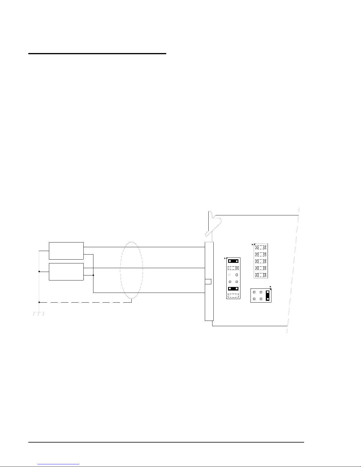
J1, J2 and J3 are unlatched header type connectors. External connections to the VL-12CT96/7 can be
made with standard cable assemblies, or with the following mating connectors:
Connector Mating Connector
J1 26-pin socket type connectors such as 3M #3399-6626
J2 10-pin socket type connectors such as 3M #3473-6610
J3 34-pin socket type connectors such as 3M #3414-6634
Figure 3-1. Mating Connectors
Figure 3-2. I/O Connector Physical Pin Locations
3-2 VL-12CT96/7 Analog & Digital I/O Card
Page 29

J1 — Analog Input Connector
Installation — External Connections
J1 Pin Differential Pesudo-Differential
1 Channel 0+ Channel 0
2 Channel 0– Channel 8
3 Analog Ground Analog Ground
4 Channel 1– Channel 9
5 Channel 1+ Channel 1
6 Analog Ground Analog Ground
7 Channel 2+ Channel 2
8 Channel 2– Channel 10
9 Analog Ground Analog Ground
10 Channel 3– Channel 11
11 Channel 3+ Channel 3
12 Analog Ground Analog Ground
13 Channel 4+ Channel 4
14 Channel 4– Channel 12
15 Analog Ground Analog Ground
16 Channel 5– Channel 13
17 Channel 5+ Channel 5
18 Analog Ground Analog Ground
19 Channel 6+ Channel 6
20 Channel 6– Channel 14
21 Analog Ground Analog Ground
22 Channel 7– Channel 15
23 Channel 7+ Channel 7
24 Analog Ground Analog Ground
25 PD PD
26 N/C N/C
Single Ended or
Figure 3-3. J1 – Analog Input Connector Pinout
Channel 0 to 15. Analog voltages are applied to these inputs for A/D conversion. In single-ended
configuration, these inputs are referenced to Analog Ground. In pseudo-differential configuration,
these inputs are considered “high side” (+) inputs and are referenced to PD.
Channel 0+ to 7+. Differential “high side” voltages are applied to these inputs for A/D conversion. Each
input is referenced to a corresponding differential “low side” (–) input.
Channel 0– to 7–. Differential “low side” voltages are applied to these inputs for A/D conversion. Each
input is referenced to a corresponding differential “high side” (+) input.
PD — Pseudo Differential “Low Side”. All “low side” (–) pseudo-differential analog voltages are connected
together and brought to this pin for differential reference.
Analog Ground. This signal is the on-board analog ground. In single-ended mode, all analog inputs are
referenced to this signal. In differential mode, a return path for the input bias currents of the on-board
instrumentation amplifiers may be connected to this pin. The use of multiple ground connections is
recommended to maintain a high degree of signal integrity.
N/C — No Connection. This signal is not connected to on-board circuitry. It has no function on the
VL-12CT96/7.
VL-12CT96/7 Analog & Digital I/O Card 3-3
Page 30

Installation — External Connections
J2 — Analog Output Connector
J2 Pin Signal Name Function
1 AGND Analog Ground
2 DA0V Channel 0 Voltage Output
3 DA0S Channel 0 Sense
4 AGND Analog Ground
5 LP0 Channel 0 Loop Power
6 DA0I Channel 0 Current Output
7 AGND Analog Ground
8 DA1V Channel 1 Voltage Output
9 DA1S Channel 1 Sense
10 AGND Analog Ground
Figure 3-4. J2 – Analog Output Connector Pinout
DA0V, DA1V — Channel 0 & 1 Voltage Output. Analog voltage outputs referenced to analog ground. Each
signal can source or sink up to 5 mA.
DA0S, DA1S — Channel 0 & 1 Sense. Remote sense inputs. Used to compensate for the voltage drop which
occurs when using long cables.
LP0 — Channel 0 Loop Power. External +15V to +30V power input. Used to provide loop power for
current loop mode.
DA0I — Channel 0 Current Output. Current loop output from channel 0.
AGND — Analog Ground. This signal is the on-board analog ground. All signals on J2 are referenced
to this signal. The use of multiple Analog Ground signals is recommended to maintain a high degree
of signal integrity.
3-4 VL-12CT96/7 Analog & Digital I/O Card
Page 31

J3—Digital I/O Connector
Installation — External Connections
J3 Pin Signal Name
1 MOD15*
2 Digital Ground
3 MOD14*
4 Digital Ground
5 MOD13*
6 Digital Ground
7 MOD12*
8 Digital Ground
9 MOD11*
10 Digital Ground
11 MOD10*
12 Digital Ground
13 MOD9*
14 Digital Ground
15 MOD8*
16 Digital Ground
17 MOD7*
18 Digital Ground
19 MOD6*
20 Digital Ground
21 MOD5*
22 Digital Ground
23 MOD4*
24 Digital Ground
25 MOD3*
26 Digital Ground
27 MOD2*
28 Digital Ground
29 MOD1*
30 Digital Ground
31 MOD0*
32 Digital Ground
33 Power
34 Digital Ground
MOD0* – MOD15*. Opto 22 bidirectional interface signals. Each signal is an open collector driver with
a 10ΚΩ pull up resistor to +5V. Input gates are attached to each signal for read-back. The open collector
driver must be in the off state to use a channel for input purposes.
used to manipulate these signals.
Power. +5V power output. When jumper V5 is installed, up to 500 mA can be drawn from this +5V
output to power the Opto 22 interface rack or other external equipment. If the I/O rack is powered by
a separate external supply, the power jumper on the I/O rack or the V5 jumper must be removed.
Digital ground. All signals on connector J3 are referenced to these digital ground connections. The use
of all ground connections is recommended to maintain a high degree of signal integrity.
VL-12CT96/7 Analog & Digital I/O Card 3-5
Figure 3-5. J3 – Digital I/O Connector Pinout
Registers PARLO and PARHI are
Page 32

3-6 VL-12CT96/7 Analog & Digital I/O Card
Page 33

Registers
Registers
Introduction
This section includes information about registers, control and status bits, and data formats. It focuses
primarily on the individual registers, the bits contained within them, and their functional descriptions.
I/O Port Mapping
The VL-12CT96/7 uses one of two I/O port maps depending upon whether the data bus is configured
for 8-bit or 16-bit operation. In 8-bit mode, registers are mapped to correspond with Analog Device’s
RTI-1265 board. In 16-bit mode, the data registers are moved to an even address boundary to facilitate
efficient single-cycle reading of the A/D data.
8-Bit Mode 8-Bit Mode 16-Bit Mode 16-Bit Mode As Shipped
Input Port Output Port Input Port Output Port Port Address Address
— DAC1HI — DAC1HI Board Address + 15 030FH
— DAC1LO — DAC1LO Board Address + 14 030EH
— DAC0HI — DAC0HI Board Address + 13 030DH
— DAC0LO — DAC0LO Board Address + 12 030CH
PARHI PARHI PARHI PARHI Board Address + 11 030BH
PARLO PARLO PARLO PARLO Board Address + 10 030AH
— CLRFLG — CLRFLG Board Address + 9 0309H
————Board Address + 8 0308H
————Board Address + 7 0307H
————Board Address + 6 0306H
— — ADCHI — Board Address + 5 0305H
ADCHI — ADCLO — Board Address + 4 0304H
ADCLO — — — Board Address + 3 0303H
— CONVERT — CONVERT Board Address + 2 0302H
— SELECT — SELECT Board Address + 1 0301H
STATUS CONTROL STATUS CONTROL Board Address + 0 0300H
Figure 4-1. I/O Port Addresses
VL-12CT96/7 Analog & Digital I/O Card 4-1
Page 34

Registers — Analog Input Registers
Analog Input Registers
The following table lists the functions assigned to each read and write register.
Write Registers Functions Page
CONTROL Interrupt, Auto-trigger, Auto increment, Scan range limit 4-2
SELECT Selects A/D channel to convert 4-4
CONVERT
CLRFLG
PARLO Parallel Port Data Low (Opto 22 Modules 8-15) 4-12
PARHI Parallel Port Data High (Opto 22 Modules 0-7) 4-12
DAC0LO D/A Channel 0 Data Low 4-10
DAC0HI D/A Channel 0 Data High 4-10
DAC1LO D/A Channel 1 Data Low 4-10
DAC1HI D/A Channel 1 Data High 4-10
Read Registers Functions Page
STATUS Busy, Done, Settling Delay, Interrupt status bits 4-6
ADCLO A/D Data Low 4-7
ADCHI A/D Data High 4-7
1
Data insensitive. Any value may be written to this port.
1
1
Triggers A/D conversion 4-5
Clears Done bit 4-5
Figure 4-2. Read and Write Register Functions
Analog Input Write Register s
Control Register
CONTROL — 0300H
7 6 5 4 3 2 1 0
D7D6D5D4D3D2D1D
Figure 4-3. Control Register
The Control register is a write register used to configure the operating mode of the VL-12CT96/7.
D7 — Not Used. This bit has no function on the VL-12CT96/7.
D6, D5 — Scan Range Limit. These two bits define and restrict the number of channels scanned in auto-
increment mode. This allows for faster throughput when only eight or four analog signals are
connected. A “1” bit in D6 or D5 forces a “0” on the multiplexer address lines MA3 or MA2 respectively.
Values other than those listed will cause channels to be skipped in groups. A board reset selects (00)
so that applications which do not use auto-increment mode are not restricted to a limited set of
channels.
0
D6 D5 Scan Range C omment
0 0 0 to 15 All 16 channels
1 0 0 to 7 Restricted range
1 1 0 to 3 Restricted range
4-2 VL-12CT96/7 Analog & Digital I/O Card
Figure 4-4. Scan Range Limit
Page 35

Registers — Analog Input Registers
(00)—Channels 0 to 15. This selection does not restrict the number of channels accessed in auto-
increment mode. (00) should be selected for applications which do not use auto-increment mode.
(10)—Channels 0 to 7. This selection causes the first eight channels to be accessed in auto-increment
mode. Channels 0 through 7 are accessed in sequence, and then repeated (modulo 8 restriction of
the value contained in the SELECT register).
(11)—Channels 0 to 3. This selection causes the first four channels to be accessed in auto-increment
mode. Channels 0 through 3 are accessed in sequence, and then repeated (modulo 4 restriction of
the value contained in the SELECT register).
D4 — Auto Increment Enable. Setting this bit to “1” places the VL-12CT96/7 in auto-increment mode. In
this mode the SELECT register increments by one after the ADCHI register is read, allowing the next
channel in sequence to be converted. The SELECT register will increment to a maximum value set
by the Scan Range Limit (bits D6 and D5 of this register) and then repeat starting again with channel
0. A settling delay set by jumper V7 is inserted after each increment. Resetting this bit to “0” disables
auto-increment mode, allowing the SELECT register to retain its value. Auto-increment is disabled
upon board reset. Auto-increment is compatible with manual and auto-trigger modes.
Before selecting auto-increment mode, the initial channel to be converted (usually channel 0) should
be selected by writing to the SELECT register.
D3 — Auto Trigger Enable. Setting this bit to “1” places the VL-12CT96/7 in auto-trigger mode. In this
mode a new A/D conversion is triggered immediately after the ADCHI register is read, eliminating the
need to trigger a conversion by writing to the CONVERT register.
There are two ways to trigger an A/D conversion: writing to the CONVERT register or reading the
ADCHI register (if auto-trigger is enabled).
To use auto-triggering, set this bit to “1,” start the first A/D “manually” by writing to the CONVERT
register, wait until Done, then read the ADCLO and ADCHI registers. From this point on, just wait
until Done and read data.
D2 — Not Used. This bit has no function on the VL-12CT96/7.
D1 — Parallel Port Interrupt Enable. Setting this bit to “1” enables parallel port interrupts. In this mode
an interrupt request is sent to the CPU when specific parallel port signal conditions are met as
determined by jumper V13. Reset this bit to “0” to disable interrupt requests from the parallel port.
See page 5-4 for further information about operating the parallel port with interrupts. An interrupt
software example is shown on page 6-8.
D0 — A/D Interrupt Enable. Setting this bit to “1” enables A/D interrupts. In this mode an interrupt
request is sent to the CPU when the A/D conversion is complete. Reset this bit to “0” to disable interrupt
requests from the A/D converter. See page 5-2 for further information about operating the A/D
converter with interrupts. An interrupt software example is shown on page 6-2.
VL-12CT96/7 Analog & Digital I/O Card 4-3
Page 36

Registers — Analog Input Registers
Channel Select Register
SELECT — 0301H
7 6 5 4 3 2 1 0
D7D6D5D4D3D2D1D
0
Figure 4-5. Channel Select Register
The SELECT register is a write register used to select the analog channel number to perform an A/D
conversion on. A word-wide output instruction to the SELECT register (out dx,ax) also writes into the
CONVERT register causing channel addressing and triggering with one CPU instruction.
D7, D6, D5, D4 — Not Used. These bits have no function on the VL-12CT96/7.
D3, D2, D1, D0 — Channel Address. These bits select the analog channel to use for A/D conversion. In
auto-increment mode, the channel address changes after each A/D conversion. In all other cases the
value remains static.
Note: The Scan Range Limit bits in the Control register affect the number stored in this register. See
page 4-2 for further information.
A settling delay set by jumper V7 is inserted whenever this register changes.
D3 D2 D1 D0 Selected Channel
0000Channel 0
0001Channel 1
0010Channel 2
0011Channel 3
0100Channel 4
0101Channel 5
0110Channel 6
0111Channel 7
1000Channel 8
1001Channel 9
1010Channel 10
1011Channel 11
1100Channel 12
1101Channel 13
1110Channel 14
1111Channel 15
Figure 4-6. Channel Selection Codes
4-4 VL-12CT96/7 Analog & Digital I/O Card
Page 37

Registers — Analog Input Registers
Convert Register
CONVERT — 0302H
7 6 5 4 3 2 1 0
D7D6D5D4D3D2D1D
0
Figure 4-7. Convert Register
The CONVERT register is a write register which, when written to, triggers (starts) an A/D conversion.
It is data insensitive; any value written to the CONVERT register will produce a trigger.
There are two ways to trigger an A/D conversion: writing to the CONVERT register or reading the
ADCHI register (if auto-trigger is enabled).
A word-wide output instruction to the SELECT register (out dx,ax) also writes into the CONVERT
register causing channel addressing and triggering with one CPU instruction.
D7-D0 — Not Used. These bits have no function on the VL-12CT96/7. Any value written triggers an A/
D conversion.
Clear Flags Register
CLRFLG — 0309H
7 6 5 4 3 2 1 0
D7D6D5D4D3D2D1D
0
Figure 4-8. Clear Flags Register
The CLRFLG register is a write register which, when written to, clears the Done bit in the STATUS
register. It is data insensitive; any value written to the CLRFLG register will clear Done.
D7-D0 — Not Used. These bits have no function on the VL-12CT96/7. Any value written will cause the
Done bit in the STATUS register to be cleared.
VL-12CT96/7 Analog & Digital I/O Card 4-5
Page 38

Registers — Analog Input Registers
Analog Input Read Registers
Status Register
STATUS — 0300H
7 6 5 4 3 2 1 0
D7D6D5D4D3D2D1D
0
Figure 4-9. Status Register
The STATUS register is a read register which contains the status of the VL-12CT96/7. It can be read
at any time to determine if an A/D conversion is complete, or if a parallel port interrupt is pending.
D7 — Busy. This bit is set to “1” when an A/D conversion is currently in progress. This bit comes directly
from the A/D converter BUSY signal and resets to “0” automatically when the A/D conversion is
complete.
D6 — Done. This bit is set to “1” when an A/D conversion has completed. It indicates that data is
available to be read from the ADCLO and ADCHI registers. When interrupts are enabled, the A/D
interrupt request signal goes active when Done is set.
The Done bit is reset to “0” when the ADCHI register is read (or it may be reset by writing to the
CLRFLG register).
D5 — Not Used. This bit has no function on the VL-12CT96/7.
D4 — Settling Delay. This bit is reset to “0” while the settling delay set by jumper V7 is in progress. The
bit is set to “1” at all other times. It is intended for factory use only.
D3, D2 — Not Used. These bits have no function on the VL-12CT96/7. They will always read as “0”.
D1 — Parallel Port Interrupt Request. Status bit indicating that a parallel port interrupt request is
pending. This bit changes from 0 to 1 when specific parallel port signal conditions are met as
determined by jumper V13. This bit changes from 1 to 0 when either PARLO or PARHI registers are
read.
4-6 VL-12CT96/7 Analog & Digital I/O Card
Page 39

Registers — Analog Input Registers
Analog Input Data Low Register
ADCLO — 0303H (8-Bit mode)
— 0304H (16-Bit mode)
7 6 5 4 3 2 1 0
D7D6D5D4D3D2D1D
0
Figure 4-10. A/D Data Low Register
The ADCLO register is a read register containing the lower 8 bits of data from the A/D conversion
results. It is used in conjunction with the ADCHI register to read the complete 12- or 16-bit data word.
After a conversion is complete (as reported by the Done bit in the STATUS register) the ADCLO register
should be read first, followed by the ADCHI register. A word-wide input instruction from the ADCLO
register (in ax,dx) will fetch data from both registers in the proper sequence. This is true for both 8bit and 16-bit modes as determined by jumper V8[1-2].
In 8-bit mode, the ADCHI and ADCLO registers are mapped to correspond with Analog Device’s RTI1265 board. In 16-bit mode, the data registers are moved to an even address boundary to facilitate
efficient single-cycle reading of the A/D data.
D7-D0 — A/D Input Data (Least Significant Byte). These bits contain data bits D7 through D0 of the
conversion results. See the A/D Data Representation section on page 4-8 for a discussion of data format.
Analog Input Data High Register
ADCHI — 0304H (8-Bit mode)
— 0305H (16-Bit mode)
7 6 5 4 3 2 1 0
D7D6D5D4D3D2D1D
0
Figure 4-11. A/D Data High Register
The ADCHI register is a read register containing the upper 8 bits of data from the A/D conversion
results. It is used in conjunction with the ADCLO register to read the complete 12- or 16-bit data word.
On the VL-12CT96, bit D3 is duplicated (sign extended) into bits D4 through D7.
When reading data, the ADCLO register should be read first, followed by the ADCHI register. See the
A/D Data Low Register section above for further information on register access.
When the ADCHI register is read the following events occur:
• The Done bit in the STATUS register is reset to “0.”
• The A/D interrupt request signal goes inactive if A/D interrupts are enabled.
• The next channel in sequence is selected if auto-increment mode enabled.
• A new A/D conversion is triggered if auto-trigger mode is enabled.
D7-D0 — A/D Input Data (Most Significant Byte). These bits contain data bits D15 through D8 of the
conversion results.
VL-12CT96/7 Analog & Digital I/O Card 4-7
Page 40

Registers — Analog Input Registers
Analog Input Data Representation (VL-12CT96, 12-Bit)
The VL-12CT96 converts applied analog voltages into 12-bit, two’s complement digital words. The full
applied analog input range is divided into 4096 steps. The output code (0000H) is associated with a midrange analog value of 0 Volts (ground). Positive analog values are represented by positive binary
numbers, whereas negative analog values are represented by negative binary numbers, i.e., -1 =
FFFFH. Bit D3 of the ADCHI register is duplicated (sign extended) into bits D4 through D7.
The formulas for calculating analog or 12-bit two’s complement digital values are given by:
Digital =————
Where:
Analog
Step
Analog = Applied voltage
Digital = A/D Conversion Data
Step = 0.00244140625 (±5V Range)
Sample 12-bit, two’s complement values are shown in the table below:
±5V Input ±10V Input ±50mV Input ±100mV Input Output Data
Voltage Voltage Voltage Voltage (Hex) (Dec) Comment
+5.0000 +10.0000 +0.0500 +0.1000 — — Out of range
+4.9976 +9.9951 +0.04998 +0.09995 07FF 2047 Maximum positive voltage
+2.5000 +5.0000 +0.0250 +0.0500 0400 1024 Positive half scale
+1.2500 +2.5000 +0.0125 +0.0250 0200 512 Positive quarter scale
+0.00244 +0.00488 +0.0000244 +0.0000488 0001 1 Positive 1 LSB
0.0000 0.0000 0.0000 0.0000 0000 0 Zero (ground input)
-0.00244 -0.00488 -0.0000244 -0.0000488 FFFF -1 Negative 1 LSB
-1.2500 -2.5000 -0.0125 -0.0250 FE00 -512 Negative quarter scale
-2.5000 -5.0000 -0.0250 -0.0500 FC00 -1024 Negative half scale
-5.0000 -10.0000 -0.0500 -0.0100 F800 -2048 Maximum negative voltage
0.0048828125 (±10V Range)
0.0000244140625 (±50 mV Range)
0.000048828125 (±100 mV Range)
Analog = Step × Digital
Figure 4-12. Two’s Complement Data Format (VL-12CT96, 12-Bit)
4-8 VL-12CT96/7 Analog & Digital I/O Card
Page 41

Registers — Analog Input Registers
Analog Input Data Representation (VL-12CT97, 16-Bit)
The VL-12CT97 converts applied analog voltages into 16-bit, two’s complement digital words. The full
applied analog input range is divided into 65536 steps. The output code (0000H) is associated with a
mid-range analog value of 0 Volts (ground). Positive analog values are represented by positive binary
numbers, whereas negative analog values are represented by negative binary numbers, i.e., -1 =
FFFFH.
The formulas for calculating analog or 16-bit two’s complement digital values are given by:
Digital =————
Where:
Analog
Step
Analog = Applied voltage
Digital = A/D Conversion Data
Step = 0.0001525878907 (±5V Range)
Sample 16-bit, two’s complement values are shown in the table below:
±5V Input ±10V Input ±50mV Input ±100mV Input Output Data
Voltage Voltage Voltage Voltage (Hex) (Dec) Comment
+5.000000 +10.000000 +0.050000 +0.100000 — — Out of range
+4.999847 +9.999695 +0.0499985 +0.099996 7FFF 32767 Maximum positive voltage
+2.500000 +5.000000 +0.025000 +0.050000 4000 16384 Positive half scale
+1.250000 +2.500000 +0.012500 +0.025000 2000 8192 Positive quarter scale
+0.000153 +0.000305 +0.0000015 +0.0000031 0001 1 Positive 1 LSB
0.000000 0.000000 0.000000 0.000000 0000 0 Zero (ground input)
-0.000153 -0.000305 -0.0000015 -0.0000031 FFFF -1 Negative 1 LSB
-1.250000 -2.500000 -0.012500 -0.025000 E000 -8192 Negative quarter scale
-2.500000 -5.000000 -0.025000 -0.050000 C000 -16384 Negative half scale
-5.000000 -10.000000 -0.050000 -0.010000 8000 -32768 Maximum negative voltage
0.0003051757813 (±10V Range)
0.000001525878907 (±50 mV Range)
0.000003051757813 (±100 mV Range)
Analog = Step × Digital
Figure 4-13. Two’s Complement Data Format (VL-12CT97, 16-Bit)
VL-12CT96/7 Analog & Digital I/O Card 4-9
Page 42

Registers — Analog Output Registers
Analog Output Registers
Analog Output Data Low Register
Channel 0 (DAC0LO) — 030CH
Channel 1 (DAC1LO) — 030EH
7 6 5 4 3 2 1 0
D7D6D5D4D3D2D1D
0
Figure 4-14. D/A Data Low Register
The DAC0LO and DAC1LO registers are write registers which receive the lower 8 bits of data used for
D/A conversion. One register is assigned for each output channel. The registers are used in conjunction
with the DAC0HI and DAC1HI registers to provide the complete 12-bit data word.
The DACxLO register should be written to first, followed by the DACxHI register. A word-wide output
instruction to the DACxLO register (out ax,dx) will write data to both registers in the proper sequence.
This is true for both 8-bit and 16-bit modes as determined by jumper V8[1-2].
Data may be written to these registers as fast as desired, since the D/A conversion is virtually
instantaneous.
D7-D0 — D/A Output Data (Least Significant Byte). The data written to these bits forms data bits D7
through D0 of the 12-bit digital value to be converted to an analog output voltage. See the D/A Data
Representation section on page 4-11 for a discussion of data format.
Analog Output Data High Register
Channel 0 (DAC0HI) — 030DH
Channel 1 (DAC1HI) — 030FH
7 6 5 4 3 2 1 0
D7D6D5D4D3D2D1D
0
Figure 4-15. D/A Data High Register
The DAC0HI and DAC1HI registers are write registers which receive the upper 4 bits of data used for
D/A conversion. One register is assigned for each output channel. The registers are used in conjunction
with the DAC0LO and DAC1LO registers to provide the complete 12-bit data word.
When writing data, the DACxLO register should be written to first, followed by the DACxHI register.
The analog output value changes when DACxHI is updated. See the D/A Data Low Register section
for further information on register access.
D7-D4 — Not Used. These bits have no function on the VL-12CT96/7.
D3-D0 — D/A Output Data (Most Significant Nibble). The data written to these bits forms data bits D11
through D8 of the 12-bit digital value to be converted to an analog output voltage. See the D/A Data
Representation section on page 4-11 for a discussion of data format.
4-10 VL-12CT96/7 Analog & Digital I/O Card
Page 43

Registers — Analog Output Registers
Analog Output Data Representation
The VL-12CT96/7 converts 12-bit, two’s complement digital words into ±5V, ±10V, or 4-20 ma output
signals. The output is divided into 4096 steps. The code 0000H produces an analog output of 0 Volts
(ground). Positive digital values produce positive analog output voltages, and negative digital values
(i.e., -1 = FFFFH) produce negative analog output voltages.
The formulas for calculating analog or two’s complement digital values are given by:
Digital =————
Where:
±5V Output ±10V Output 4-20 ma Output Output Data
Voltage Voltage Current (Hex) (Dec) Comment
+4.9976 +9.9951 20.0000 07FF 2047 Maximum positive voltage
+2.5000 +5.0000 12.0000 0400 1024 Positive half scale
+1.2500 +2.5000 8.0000 0200 512 Positive quarter scale
+0.00244 +0.00488 4.0078 0001 1 Positive 1 LSB
0.0000 0.0000 4.0000 0000 0 Zero (ground output)
-0.00244 -0.00488 Not allowed FFFF -1 Negative 1 LSB
-1.2500 -2.5000 Not allowed FE00 -512 Negative quarter scale
-2.5000 -5.0000 Not allowed FC00 -1024 Negative half scale
-5.0000 -10.0000 Not allowed F800 -2048 Maximum negative voltage
Analog
Step
Analog = Applied voltage
Digital = A/D Conversion Data
Step = 0.00244140625 (±5V Range)
0.0048828125 (±10V Range)
0.0000244140625 (±50 mV Range)
0.000048828125 (±100 mV Range)
Analog = Step × Digital
Figure 4-16. Two’s Complement Data Format
VL-12CT96/7 Analog & Digital I/O Card 4-11
Page 44

Registers — Parallel Port Registers
Parallel Por t Registers
Signal Direction
The VL-12CT96/7 parallel port signals are bidirectional. When the system is powered up, or a system
reset occurs, all of the channels are reset to inputs which causes the signal lines to go high.
Channels can be used as outputs by writing 0 or 1 to the appropriate bit in the PARHI or PARLO
register. Writing a 1 enables the open collector driver causing the signal line to go low. Writing a 0
tri-states the open collector driver, allowing the pull-up resistor to pull the signal line high.
Channels can be used as inputs by writing 0 to the appropriate bit in the PARHI or PARLO register.
Input status of the signal line can then be read by reading the same bit. Channels that are used as
inputs may be read at any time, but they must never have a 1 written to them. When writing to ports
which include both input and output channels, be certain to reset the bits corresponding to input
channels to 0.
Parallel Port Data High Register
Channel 1 (PARHI) — 030BH
7 6 5 4 3 2 1 0
D7D6D5D4D3D2D1D
0
Figure 4-17. Parallel Port Data High Register
D7-D0 — MOD0-MOD7. Data written to this register is driven onto the parallel port data signals MD0*–
MD7* on connector J3. This is an inverted data port; when a bit is set to 1 the signal line is driven low,
when a bit is reset to 0 the signal line is driven high.
Data read from this register returns the current
inverted input state of the parallel port signals. However, if a 1 has been written to a particular bit
position, that signal line is set to an output. Data will always read as 1 in this case. Please note:
D7=MOD0, D0=MOD7.
Parallel Port Data Low Register
Channel 1 (PARLO) — 030AH
7 6 5 4 3 2 1 0
D7D6D5D4D3D2D1D
0
Figure 4-18. Parallel Port Data Low Register
D7-D0 — MOD8-MOD15. Data written to this register is driven onto the parallel port data signals MD8*–
MD15* on connector J3. This is an inverted data port; when a bit is set to 1 the signal line is driven
low, when a bit is reset to 0 the signal line is driven high.
current inverted input state of the parallel port signals. However, if a 1 has been written to a particular
bit position, that signal line is set to an output. Data will always read as 1 in this case. Please note:
D7=MOD8, D0=MOD15.
4-12 VL-12CT96/7 Analog & Digital I/O Card
Data read from this register returns the
Page 45

Operation
Operation
This section describes how to operate the VL-12CT96/7. Analog input, analog output, and digital I/O
are discussed. Code examples written in 80188 assembly language are included in the next section.
Analog Input
Polled Mode Analog Input
Polled mode operation is the simplest method of analog input. In this mode, software is in control of
the analog input process at all times. It is the responsibility of the CPU to start each new A/D
conversion as desired, and to read the digital results upon completion.
Polled Mode Steps
• Channel selection
• Trigger A/D conversion
• Wait until done
• Read data
Channel selection
Output the desired channel number to the SELECT register. See page 4-4 for further information.
After the first channel selection, this step can be skipped for multiple conversions of the same channel.
This will eliminate the settling delay which is inserted every time the SELECT register is written to.
A word-wide output instruction to this register (out dx,ax) also writes into the CONVERT register
causing channel addressing and triggering with one CPU instruction.
Trigger A/D conversion
Output to the CONVERT register. The register is data insensitive, any value written to it will start
an A/D conversion. See page 4-5 for further information.
Wait until done
Read the STATUS register repeatedly until the Done bit is set to “1.” See page 4-6 for further
information.
Read data
Input from the ADCLO register first, followed by the ADCHI register. A word-wide input instruction
from the ADCLO register (in ax,dx) will fetch data from both the registers in the proper sequence. See
page 4-7 for further information.
VL-12CT96/7 Analog & Digital I/O Card 5-1
Page 46

Operation — Analog Input
Interrupt Mode Analog Input
Interrupt mode eliminates the need to repeatedly poll the STATUS register for Done status. This frees
up the CPU to execute unrelated code while the VL-12CT96/7 is busy with an A/D conversion. This
is especially useful when using long settling delays. Another use for interrupts is for handling auto
triggered applications.
Interrupt Mode Steps
• Interrupt Service Routine
• Initialize VL-12CT96/7 for interrupt mode
• Initialize VL-12CT96/7 for Auto-trigger (if desired)
• Initialize interrupt controller
• Initialize CPU to receive interrupt
• Channel selection
• Initialize VL-12CT96/7 for Auto-increment (if desired)
• Trigger A/D conversion
Interrupt Service Routine
The interrupt service routine reads A/D conversion results from the VL-12CT96/7 and stores the data
somewhere. Data is input from the ADCLO register first, followed by the ADCHI register. A wordwide input instruction from the ADCLO register (in ax,dx) will fetch data from both registers in the
proper sequence. Reading the ADCHI register clears the interrupt request.
The interrupt service routine can be written to select a different channel or trigger a new conversion.
Initialize VL-12CT96/7 for interrupt mode
Set bit D0 in the CONTROL register. See page 4-2 for further information.
Initialize VL-12CT96/7 for Auto-trigger (if desired)
Set bit D3 in the CONTROL register. See page 4-2 for further information.
Auto-trigger mode is optional when using interrupts. Use it when you want to perform a continuous
stream of analog input conversions. Auto-trigger mode eliminates the CPU overhead of writing to the
CONVERT register.
Initialize interrupt controller
This involves setting up interrupt vector registers, priority, and unmasking. See your interrupt
controller instruction manual for further information.
Initialize CPU to receive interrupts
This involves preparing the interrupt vector table, and enabling interrupts. See your CPU instruction
manual for further information.
Channel selection
Output the desired channel number to the SELECT register. See page 4-4 for further information.
5-2 VL-12CT96/7 Analog & Digital I/O Card
Page 47

Operation — Analog Output
Initialize VL-12CT96/7 for Auto-increment (if desired)
Set bit D4 in the CONTROL register. See page 4-2 for further information.
Auto-increment mode is optional when using interrupts. Use it when you want to convert a series of
analog input channels beginning with the channel in the SELECT register. Auto-increment mode
eliminates the CPU overhead of writing to the SELECT register. When disabled, the VL-12CT96/7 will
convert the channel in the SELECT register repeatedly without a settling delay penalty.
Trigger A/D conversion
Write any value to the CONVERT register to begin. An interrupt is generated when the VL-12CT96/
7 completes an A/D conversion.
Analog Output
Writing to a VL-12CT96/7 analog output channel is as simple as writing 12 bits of data to the desired
output registers. Each channel has two registers, DACxLO and DACxHI. DACxLO should be written
to first, followed by DACxHI. When DACxHI is updated the analog output value will change. See page
4-10 for further information.
• Determine address of desired channel.
• Output data to channel register: Low byte first, high byte second; or a single 16-bit output.
Digital I/O
Signal Direction
All of the VL-12CT96/7 parallel port signals are bidirectional. The logic state of any channel can be
read by reading the PARHI or PARLO register. The logic level on any channel can be manipulated by
writing a 1 or 0 to the apprioriate bit in the PARHI or PARLO register.
If a channel is driven low, that channel cannot be used for input until it is released. See page 4-12 for
further information.
• Initialize by writing zeros to all input channels.
• Output by writing bytes or words to PARLO and PARHI registers. Always write zeros to input
channels.
• Input by reading bytes or words from PARLO and PARHI registers.
VL-12CT96/7 Analog & Digital I/O Card 5-3
Page 48

Operation — System Reset
Signal Inversion
All parallel port circuits on the VL-12CT96/7 board are inverting. A high logic level on connector J3
is represented by a 0 in the PARLO or PARHI register, and a low logic level is represented by a 1.
Since Opto 22 modules invert the logic sense of signals passed through them, the register-to-module
interface is effectively positive logic. The resulting data interface levels between the VL-12CT96/7 and
I/O rack modules are shown in Figure 5-1.
Data I/O Output Input I/O Data
Written Pin Modules Modules Pin Read
0 (1) Power off Voltage absent (1) 0
1 (0) Power on Voltage present (0) 1
Figure 5-1. I/O Module Data Interface
Digital Input
The logic state of the parallel input channels can be read at any time by reading the PARLO or PARHI
registers. Simply choose the correct register and read it as an 8-bit quantity. If desired, both registers
can be read with a single 16-bit input transaction (in ax,dx) by addressing PARLO. This works with
both 8 and 16-bit data modes. If using STD 32, this data transfer will take a single bus cycle. See page
4-12 for further information on register access.
Interrupt Mode Digital Input
One of four parallel port signals can be selected by jumper V13 to trigger an interrupt request when
the logic state on these signals changes state.
Two edge options are available: single edge, and double edge mode. Single edge mode generates an
interrupt when the selected input signal (at connector J3) switches from high-to-low. Double edge
mode generates an interrupt on both high-to-low and low-to-high transitions.
The interrupt request signal is cleared when either the PARLO or PARHI register is read.
Digital Output
The logic state of any parallel output channel can be manipulated at any time by writing to the PARLO
or PARHI registers. Simply choose the correct register and write the digital value to it as an 8-bit
quantity. If desired, both registers can be written to with a single 16-bit output transaction (out dx,ax)
by addressing PARLO. This works with both 8 and 16-bit data modes. If using STD 32, this data
transfer will take a single bus cycle. See page 4-12 for further information on register access.
System Reset
When the card is powered up, or a system reset occurs, the following happens:
• Analog input channel address is reset to zero.
• Analog input status flags are cleared.
• Analog outputs are reset to 0 volts.
• Digital outputs are reset to their inactive high states.
5-4 VL-12CT96/7 Analog & Digital I/O Card
Page 49

Software Examples
Software Examples
This section shows some software examples written in Intel compatible assembly language to assist you
in constructing your own software routines. The interrupt code examples are written specifically for
use with VersaLogic’s 80188 CPU card, VL-188.
Analog Input Code Example
The following example reads channel 0 into the AX register. It assumes that the board is addressed
at location 0300H.
The key program sections are:
READ : Reads A/D channel 0 into AX register.
BUSY : Location where program loops waiting for A/D conversion to complete.
0000 .model small
0000 .stack
0000 .data
0000 .code
;VL-12CT96/7 I/O PORT ADDRESSES
= 0300 control equ 0300h ;Control Register
= 0300 status equ 0300h ;Status Register
= 0301 select equ 0301h ;Channel Select Register
= 0302 convert equ 0302h ;Convert Register
= 0303 adclo equ 0303h ;A/D Data Low Register
= 0304 adchi equ 0304h ;A/D Data High Register
= 0309 clrflg equ 0309h ;Clear Flags Register
= 030A parlo equ 030Ah ;Parallel Port Data Low Register
= 030B parhi equ 030Bh ;Parallel Port Data High Register
= 030C dac0lo equ 030Ch ;D/A Channel 0 Data Low Register
= 030D dac0hi equ 030Dh ;D/A Channel 0 Data High Register
= 030E dac1lo equ 030Eh ;D/A Channel 1 Data Low Register
= 030F dac1hi equ 030Fh ;D/A Channel 1 Data High Register
;MAINLINE CODE
0000
0000 B0 00 mov al,00h ;Select channel 0
0002 BA 0301 mov dx,select
0005 EE out dx,al
0006 BA 0302 mov dx,convert ;Trigger conversion
0009 EE out dx,al
000A BA 0300 mov dx,status ;Standby until done
000D EC
000E A8 40 test al,01000000b
0010 74 FB jz busy
read:read:
read: ;READ CHANNEL 0 INTO AX REGISTER
read:read:
busy:busy:
busy: in al,dx
busy:busy:
0012 BA 0303 mov dx,adclo ;Read data into AX register
0015 ED in ax,dx
end read
VL-12CT96/7 Analog & Digital I/O Card 6-1
Page 50

Software Examples — Analog Input Interrupt Mode
Analog Input Interrupt Mode Code Example
The following code example shows how to use analog input with interrupts. An A/D conversion is
started in the normal manner, when the data is ready, an interrupt is generated.
The key program sections are:
MAIN : Execution begins here. Installation and setup are coordinated here.
INIT_188 : Initializes the VL-188 interrupt controller to accept interrupts from the STD
Bus. Installs interrupt vector into low RAM.
INIT_1296 : Initializes the VL-12CT96/7 to generate interrupts upon conversion complete.
ISR : Interrupt Service Routine. This subroutine is responsible for reading, process-
ing, and/or storing the A/D results from the VL-12CT96/7.
0000 .model small
0000 .stack
0000 .data
0000 ???? value dw ? ;Holding variable for A/D input
0002 .code
0000 vector segment at 0 ;CPU Interrupt Vector Table
0000 vector ends
;VL-12CT96/7 I/O PORT ADDRESSES
= 0300 control equ 0300h ;Control Register
= 0300 status equ 0300h ;Status Register
= 0301 select equ 0301h ;Channel Select Register
= 0302 convert equ 0302h ;Convert Register
= 0303 adclo equ 0303h ;A/D Data Low Register
= 0304 adchi equ 0304h ;A/D Data High Register
= 0309 clrflg equ 0309h ;Clear Flags Register
= 030A parlo equ 030Ah ;Parallel Port Data Low Register
= 030B parhi equ 030Bh ;Parallel Port Data High Register
= 030C dac0lo equ 030Ch ;D/A Channel 0 Data Low Register
= 030D dac0hi equ 030Dh ;D/A Channel 0 Data High Register
= 030E dac1lo equ 030Eh ;D/A Channel 1 Data Low Register
= 030F dac1hi equ 030Fh ;D/A Channel 1 Data High Register
;VL-188 I/O PORT ADDRESSES
= FF22 eoi equ 0FF22h ;80188 EOI Register
= FF3A int1 equ 0FF3Ah ;80188 INT1 Control Register
0000
0000 B8 0000s mov ax,@data ;Set data segment register
0003 8E D8 mov ds,ax
0005 C7 06 0000r 0000 mov value,0 ;Initialize holding variable
000B E8 000D call init_188 ;Initialize VL-188 interrupts
000E E8 0028 call init_1296 ;Initialize VL-12CT96/7 interrupts
0011 FB sti ;Enable CPU interrupt flag
0012 BA 0301 mov dx,select ;Begin conversion of channel 0
0015 B8 0000 mov ax,0
0018 EF out dx,ax
;VL-12CT96/7 will generate an interrupt
;request when the conversion is
;complete (takes about 15 uS)
;The ISR is responsible for reading
;the data.
0019 EB FE stop: jmp stop ;Rest of mainline goes here
001B
main:main:
main: ;MAINLINE CODE
main:main:
init_188:init_188:
init_188: ;VL-188 INTERRUPT INITIALIZATION
init_188:init_188:
6-2 VL-12CT96/7 Analog & Digital I/O Card
Page 51

Software Examples — Analog Input Interrupt Mode
001B BA FF3A mov dx,int1 ;INT1 CONTROL REGISTER
001E B8 0017 mov ax,0017h ;D15 0 0 — = Non Functional Bit
0021 EF out dx,ax ;D14 0 0 — = Non Functional Bit
;D13 0 0 — = Non Functional Bit
;D12 0 0 — = Non Functional Bit
;D11 0 0 — = Non Functional Bit
;D10 0 0 — = Non Functional Bit
;D9 0 0 — = Non Functional Bit
;D8 0 0 — = Non Functional Bit
;D7 0 0 — = Non Functional Bit
;D6 0 SFNM = Normal
;D5 0 C = Non Cascade
;D4 1 LTM = Level Trigger
;D3 0 MSK = Non masked
;D2 1 PR2 = Priority 7
;D1 1 PR1 = Priority 7
;D0 1 PR0 = Priority 7
;Un-mask STD Bus INTRQ* interrupts
;and set to non-cascade mode because
;VL-12CT96/7 does not provide interrupt
;vector. CPU will internally
;generate type code 13.
0022 B8 0000s mov ax,vector ;Point data segment register to
0025 8E D8 mov ds,ax ;interrupt vector area
0027 C7 06 0034 0040r mov word ptr ds:[34h],offset isr
002D C7 06 0036 0000s mov word ptr ds:[36h],seg isr
0033 B8 0000s mov ax,@data ;Point data segment register to
0036 8E D8 mov ds,ax ;variable storage area
0038 C3 ret
0039
0039 B0 01 mov al,01h ;CONTROL REGISTER
003B BA 0300 mov dx,control ;D7 0 Scan Range Limit = No limit
003E EE out dx,al ;D6 0 Scan Range Limit = No limit
003F C3 ret ;D5 0 Scan Range Limit = No limit
;D4 0 Auto Increment = Off
;D3 0 Auto Trigger = Off
;D2 0 Non Functional Bit = 0
;D1 0 Parallel Int Enable = Off
;D0 1 A/D Int Enable = On
0040
0040 50 push ax ;Save CPU registers
0041 52 push dx
0042 1E push ds
0043 B8 0000s mov ax,@data ;Set data segment register
0046 8E D8 mov ds,ax
0048 BA 0303 mov dx,adclo ;Read A/D results
004B ED in ax,dx
004C A3 0000r mov value,ax ;Store results into variable
;
;Additional processing code is
;inserted here if desired.
;This could include mathematic
;manipulation, data storage,
;limit checks, etc.
004F isr_exit:
004F BA FF22 mov dx,eoi ;Issue a Non-Specific End-Of-Interrupt
0052 B8 8000 mov ax,8000h ;command to 80188 interrupt controller
init_1296:init_1296:
init_1296: ;VL-12CT96/7 INTERRUPT INITIALIZATION
init_1296:init_1296:
isr:isr:
isr: ;INTERRUPT SERVICE ROUTINE
isr:isr:
VL-12CT96/7 Analog & Digital I/O Card 6-3
Page 52

Software Examples — Analog Output
0055 EF out dx,ax
0056 1F pop ds ;Restore CPU registers
0057 5A pop dx
0058 58 pop ax
0059 CF iret ;Return to interrupted program
end main
Analog Output Code Example
The following code example shows how to operate the D/A converter.
The key program section is:
WRITE : Outputs zero volts to A/D channel 0.
0000 .model small
0000 .stack
0000 .data
0000 .code
;VL-12CT96/7 I/O PORT ADDRESSES
= 0300 control equ 0300h ;Control Register
= 0300 status equ 0300h ;Status Register
= 0301 select equ 0301h ;Channel Select Register
= 0302 convert equ 0302h ;Convert Register
= 0303 adclo equ 0303h ;A/D Data Low Register
= 0304 adchi equ 0304h ;A/D Data High Register
= 0309 clrflg equ 0309h ;Clear Flags Register
= 030A parlo equ 030Ah ;Parallel Port Data Low Register
= 030B parhi equ 030Bh ;Parallel Port Data High Register
= 030C dac0lo equ 030Ch ;D/A Channel 0 Data Low Register
= 030D dac0hi equ 030Dh ;D/A Channel 0 Data High Register
= 030E dac1lo equ 030Eh ;D/A Channel 1 Data Low Register
= 030F dac1hi equ 030Fh ;D/A Channel 1 Data High Register
0000
0000 BA 030C mov dx,dac0lo ;Select channel 0
0003 B8 0000 mov ax,0000h ;0000h = Zero volts in 2’s complement
mode
0006 EF out dx,ax ;Output data to D/A converter
end write
write:write:
write: ;OUTPUT ZERO VOLTS ON CHANNEL 0
write:write:
6-4 VL-12CT96/7 Analog & Digital I/O Card
Page 53

Software Examples — Parallel Port
Parallel Por t Code Example
The following code example shows how to operate the digital I/O port. In this example, half of the port
signals are arbitrarily defined as inputs.
The key program sections are:
MAIN : Direction initialization and calling syntax.
INIT_PAR : Defines the signal direction of the parallel port channels. All output channels
are turned off.
CHANNEL_READ : Returns the ON/OFF state of the channel specified by the AL register in the
CPU carry flag.
CHANNEL_ON : Turns the channel specified by the AL register ON.
CHANNEL_OFF : Turns the channel specified by the AL register OFF.
0000 .model small
0000 .stack
0000 .data
0000 ???? dir dw ? ;Port direction pattern
0002 .code
;VL-12CT96/7 I/O PORT ADDRESSES
= 0300 control equ 0300h ;Control Register
= 0300 status equ 0300h ;Status Register
= 0301 select equ 0301h ;Channel Select Register
= 0302 convert equ 0302h ;Convert Register
= 0303 adclo equ 0303h ;A/D Data Low Register
= 0304 adchi equ 0304h ;A/D Data High Register
= 0309 clrflg equ 0309h ;Clear Flags Register
= 030A parlo equ 030Ah ;Parallel Port Data Low Register
= 030B parhi equ 030Bh ;Parallel Port Data High Register
= 030C dac0lo equ 030Ch ;D/A Channel 0 Data Low Register
= 030D dac0hi equ 030Dh ;D/A Channel 0 Data High Register
= 030E dac1lo equ 030Eh ;D/A Channel 1 Data Low Register
= 030F dac1hi equ 030Fh ;D/A Channel 1 Data High Register
0000
0000 B8 0000s mov ax,@data ;Set data segment register
0003 8E D8 mov ds,ax
0005 B8 00FF mov ax,00FFh ;Parallel port direction control
0008 E8 001C call init_par ;D15 0 MD0 Direction = Input
;D14 0 MD1 Direction = Input
;D13 0 MD2 Direction = Input
;D12 0 MD3 Direction = Input
;D11 0 MD4 Direction = Input
;D10 0 MD5 Direction = Input
;D9 0 MD6 Direction = Input
;D8 0 MD7 Direction = Input
;D7 1 MD8 Direction = Output
;D6 1 MD9 Direction = Output
;D5 1 MD10 Direction = Output
;D4 1 MD11 Direction = Output
;D3 1 MD12 Direction = Output
;D2 1 MD13 Direction = Output
;D1 1 MD14 Direction = Output
;D0 1 MD15 Direction = Output
main:main:
main: ;MAINLINE CODE
main:main:
000B B0 0F mov al,15 ;Turn MD15 ON
000D E8 0031 call channel_on
0010 B0 0F mov al,15 ;Turn MD15 OFF
VL-12CT96/7 Analog & Digital I/O Card 6-5
Page 54

Software Examples — Parallel Port
0012 E8 0045 call channel_off
0015 B0 00 mov al,0 ;Acquire ON/OFF state of channel 0
0017 E8 001A call channel_read
001A 72 06 jc on_code ;Execute conditional branch
001C off_code: ;Process OFF code here
001C 90 nop
001D 90 nop
001E 90 nop
001F EB 04 90 jmp stop
0022 on_code: ;Process ON code here
0022 90 nop
0023 90 nop
0024 90 nop
0025 EB FE stop: jmp stop ;Rest of mainline program here
0027
;AX=Direction Pattern
;1=Output 0=Input
;Turns all output channels off
0027 52 push dx
0028 A3 0000r mov dir,ax ;Save pattern to guarantee we never
;output a “1” to an input channel
002B B8 0000 mov ax,0000h ;Turn all output channels off
002E BA 030A mov dx,parlo
0031 EF out dx,ax
0032 5A pop dx
0033 C3 ret
0034
;AL=Channel number (00h to 0Fh).
;Carry flag reflects logic state
;of input signal upon exit. Use
;conditional jump instructions
;JC or JNC as appropriate to
;control program flow after
;calling this subroutine.
;Carry=1 if selected input = ON
;Carry=0 if selected input = OFF
0034 52 push dx
0035 8A C8 mov cl,al ;Use CL register as a shift counter
0037 FE C1 inc cl ;Always want at least one shift
0039 BA 030A mov dx,parlo
003C ED in ax,dx ;Read the parallel port registers
init_par:init_par:
init_par: ;Initializes Parallel Port
init_par:init_par:
channel_read:channel_read:
channel_read: ;Used to read input channels.
channel_read:channel_read:
003D D3 E0 shl ax,cl ;Shift the channel bit into carry
003F 5A pop dx
0040 C3 ret
0041
;AL=Channel Number. If an input
;channel is specified, nothing
;happens.
0041 53 push bx
0042 51 push cx
0043 52 push dx
0044 BB 8000 mov bx,8000h ;Setup initial mask position
0047 8A C8 mov cl,al ;Use channel # as rotate counter
channel_on:channel_on:
channel_on: ;Used to turn an output channel ON
channel_on:channel_on:
6-6 VL-12CT96/7 Analog & Digital I/O Card
Page 55

Software Examples — Parallel Port
0049 D3 EB shr bx,cl ;Rotate right to align mask
004B BA 030A mov dx,parlo ;Fetch existing state of ports
004E ED in ax,dx
004F 0B C3 or ax,bx ;Set bit to turn channel on
0051 23 06 0000r and ax,dir ;Clear bits associated with input
0055 EE out dx,al ;Update parallel port
0056 5A pop dx ;Restore registers
0057 59 pop cx
0058 5B pop bx
0059 C3 ret
005A
;AL=Channel Number. If an input
;channel is specified, nothing
;happens.
005A 53 push bx
005B 51 push cx
005C 52 push dx
005D BB 7FFF mov bx,7FFFh ;Setup initial mask position
0060 8A C8 mov cl,al ;Use channel # as rotate counter
0062 D3 EB shr bx,cl ;Rotate right to align mask
0064 BA 030A mov dx,parlo ;Fetch existing state of ports
0067 ED in ax,dx
0068 23 C3 and ax,bx ;Clear bit to turn channel on
006A 23 06 0000r and ax,dir ;Clear bits associated with input
006E EE out dx,al ;Update parallel port
006F 5A pop dx ;Restore registers
0070 59 pop cx
0071 5B pop bx
0072 C3 ret
end main
channel_off:channel_off:
channel_off: ;Used to turn an output channel OFF
channel_off:channel_off:
VL-12CT96/7 Analog & Digital I/O Card 6-7
Page 56

Software Examples — Parallel Port Interrupt Mode
Parallel Por t Interrupt Mode Code Example
The following code example shows how to operate the digital I/O port using interrupts. In this example,
half of the port signals are arbitrarily defined as inputs. Signal activity on MD0, MD1, MD2, or MD3
(as selected by jumper V13) will generate an interrupt request.
The key program sections are:
MAIN : System initialization and calling syntax.
INIT_188 : Initializes the VL-188 (CPU) interrupt controller to accept interrupts from the
STD Bus. Installs interrupt vector into low RAM.
INIT_1296 : Enables parallel port interrupts on the VL-12CT96/7.
INIT_PAR : Defines the signal direction of the parallel port channels. All output channels
are turned off.
ISR : Interrupt Service Routine. This subroutine is responsible for reading, and
processing the parallel port input from the VL-12CT96/7.
0000 .model small
0000 .stack
0000 .data
0000 ???? dir dw ? ;Port direction pattern
0002 .code
0000 vector segment at 0 ;CPU Interrupt Vector Table
0000 vector ends
;VL-12CT96/7 I/O PORT ADDRESSES
= 0300 control equ 0300h ;Control Register
= 0300 status equ 0300h ;Status Register
= 0301 select equ 0301h ;Channel Select Register
= 0302 convert equ 0302h ;Convert Register
= 0303 adclo equ 0303h ;A/D Data Low Register
= 0304 adchi equ 0304h ;A/D Data High Register
= 0309 clrflg equ 0309h ;Clear Flags Register
= 030A parlo equ 030Ah ;Parallel Port Data Low Register
= 030B parhi equ 030Bh ;Parallel Port Data High Register
= 030C dac0lo equ 030Ch ;D/A Channel 0 Data Low Register
= 030D dac0hi equ 030Dh ;D/A Channel 0 Data High Register
= 030E dac1lo equ 030Eh ;D/A Channel 1 Data Low Register
= 030F dac1hi equ 030Fh ;D/A Channel 1 Data High Register
;VL-188 I/O PORT ADDRESSES
= FF22 eoi equ 0FF22h ;80188 EOI Register
= FF3A int1 equ 0FF3Ah ;80188 INT1 Control Register
0000
0000 B8 0000s mov ax,@data ;Set data segment register
0003 8E D8 mov ds,ax
0005 B8 00FF mov ax,00FFh ;Parallel port direction control
0008 E8 002E call init_par ;D15 0 MD0 Direction = Input
;D14 0 MD1 Direction = Input
;D13 0 MD2 Direction = Input
;D12 0 MD3 Direction = Input
;D11 0 MD4 Direction = Input
;D10 0 MD5 Direction = Input
;D9 0 MD6 Direction = Input
;D8 0 MD7 Direction = Input
;D7 1 MD8 Direction = Output
;D6 1 MD9 Direction = Output
;D5 1 MD10 Direction = Output
;D4 1 MD11 Direction = Output
main:main:
main: ;MAINLINE CODE
main:main:
6-8 VL-12CT96/7 Analog & Digital I/O Card
Page 57

Software Examples — Parallel Port Interrupt Mode
;D3 1 MD12 Direction = Output
;D2 1 MD13 Direction = Output
;D1 1 MD14 Direction = Output
;D0 1 MD15 Direction = Output
000B E8 0006 call init_188 ;Initialize VL-188 interrupts
000E E8 0021 call init_1296 ;Initialize VL-12CT96/7 interrupts
0011 FB sti ;Enable CPU interrupt flag
0012 EB FE stop: jmp stop ;Rest of mainline goes here
0014
0014 BA FF3A mov dx,int1 ;INT1 CONTROL REGISTER
0017 B8 0017 mov ax,0017h ;D15 0 0 — = Non Functional Bit
001A EF out dx,ax ;D14 0 0 — = Non Functional Bit
;D13 0 0 — = Non Functional Bit
;D12 0 0 — = Non Functional Bit
;D11 0 0 — = Non Functional Bit
;D10 0 0 — = Non Functional Bit
;D9 0 0 — = Non Functional Bit
;D8 0 0 — = Non Functional Bit
;D7 0 0 — = Non Functional Bit
;D6 0 SFNM = Normal
;D5 0 C = Non Cascade
;D4 1 LTM = Level Trigger
;D3 0 MSK = Non masked
;D2 1 PR2 = Priority 7
;D1 1 PR1 = Priority 7
;D0 1 PR0 = Priority 7
;Un-mask STD Bus INTRQ* interrupts
;and set to non-cascade mode because
;VL-12CT96/7 does not provide interrupt
;vector. CPU will internally
;generate type code 13.
001B B8 0000s mov ax,vector ;Point data segment register to
001E 8E D8 mov ds,ax ;interrupt vector area
0020 C7 06 0034 0046r mov word ptr ds:[34h],offset isr
0026 C7 06 0036 0000s mov word ptr ds:[36h],seg isr
002C B8 0000s mov ax,@data ;Point data segment register to
002F 8E D8 mov ds,ax ;variable storage area
0031 C3 ret
init_188:init_188:
init_188: ;VL-188 INTERRUPT INITIALIZATION
init_188:init_188:
0032
0032 B0 02 mov al,02h ;CONTROL REGISTER
0034 BA 0300 mov dx,control ;D7 0 Scan Range Limit = No limit
0037 EE out dx,al ;D6 0 Scan Range Limit = No limit
0038 C3 ret ;D5 0 Scan Range Limit = No limit
;D4 0 Auto Increment = Off
;D3 0 Auto Trigger = Off
;D2 0 Non Functional Bit = 0
;D1 0 Parallel Int Enable = On
;D0 1 A/D Int Enable = Off
0039
;AX=Direction Pattern
;1=Output 0=Input
;Turns all output channels off
0039 52 push dx
003A A3 0000r mov dir,ax ;Save pattern to guarantee we never
;output a “1” to an input channel
003D B8 0000 mov ax,0000h ;Turn all output channels off
0040 BA 030A mov dx,parlo
VL-12CT96/7 Analog & Digital I/O Card 6-9
init_1296:init_1296:
init_1296: ;VL-12CT96/7 INTERRUPT INITIALIZATION
init_1296:init_1296:
init_par:init_par:
init_par: ;Initializes Parallel Port
init_par:init_par:
Page 58

Software Examples — Parallel Port Interrupt Mode
0043 EF out dx,ax
0044 5A pop dx
0045 C3 ret
0046
0046 50 push ax ;Save CPU registers
0047 52 push dx
0048 1E push ds
0049 B8 0000s mov ax,@data ;Set data segment register
004C 8E D8 mov ds,ax
004E BA 030A mov dx,parlo ;Read parallel port
0051 ED in ax,dx
;Additional processing code is
;inserted here if desired.
;This could include mathematic
;manipulation, data storage,
;limit checks, etc.
0052 isr_exit:
0052 BA FF22 mov dx,eoi ;Issue a Non-Specific End-Of-Interrupt
0055 B8 8000 mov ax,8000h ;command to 80188 interrupt controller
0058 EF out dx,ax
0059 1F pop ds ;Restore CPU registers
005A 5A pop dx
005B 58 pop ax
005C CF iret ;Return to interrupted program
end main
isr:isr:
isr: ;INTERRUPT SERVICE ROUTINE
isr:isr:
6-10 VL-12CT96/7 Analog & Digital I/O Card
Page 59

Calibration
Calibration
The VL-12CT96/7 is calibrated before shipment. However, it may be desirable to recalibrate the card
after installation, and approximately once per year (depending upon the accuracy requirements of the
application).
Analog Input Calibration
Required Equipment
• A voltmeter with resolution and accuracy to ½ LSB of the input range being used.
• A low noise DC voltage source capable of providing a stable reference standard for calibration.
• A small flat blade screwdriver.
Calibration Procedure
• Jumper card for single ended input mode.
• Disconnect cable from connector J1. Use a shorting jumper to short pins 1 and 3 on connector
J1. This applies 0.000 volts (AGND) to channel 0.
• Using a program to continuously read channel 0, adjust the ZERO pot until the reading centers on 0000H.
• Attach the voltmeter to the voltage source, and adjust (per the table below) to the calibration
voltage appropriate for the input range being used.
• Using a program to continuously read channel 0, adjust the “GAIN” pot until the reading
centers on 07FBH (VL-12CT96) or 7FFBH (VL-12CT97).
————————————Input Range————————————
±5V ±10V ±50mV ±100mV
12 Bit Resolution +4.987793 +9.975586 +0.049878 +0.099756
16 Bit Resolution +4.999237 +9.998474 +0.049992 +0.099984
Figure 7-1. Analog Input Calibration Voltages
VL-12CT96/7 Analog & Digital I/O Card 7-1
Page 60

Calibration — Analog Output (Voltage Mode)
Analog Output Calibration (Voltage Mode)
Required Equipment
• A voltmeter with resolution and accuracy to ½ LSB of the output range being used.
• A small flat blade screwdriver.
Calibration Procedure
Channel 0
• Disconnect cable from connector J2.
• Connect the voltmeter to channel 0 on connector J2; positive lead (red) to pin 2, negative lead
(black) to pin 1.
• Write 0800H to channel 0.
• Adjust Z0 pot until voltage is exactly -10.0000V.
• Write 07FFH to channel 0.
• If using ±5V range, adjust G0 pot until voltage is exactly +4.997559V.
If using ±10V range, adjust G0 pot until voltage is exactly +9.995117V.
Channel 1
• Connect the voltmeter to channel 1 on connector J2; positive lead (red) to pin 8, negative lead
(black) to pin 7.
• Write 0800H to channel 1.
• Adjust Z1 pot until voltage is exactly -10.0000V.
• Write 07FFH to channel 1.
• If using ±5V range, adjust G1 pot until voltage is exactly +4.997559V.
If using ±10V range, adjust G1 pot until voltage is exactly +9.995117V.
7-2 VL-12CT96/7 Analog & Digital I/O Card
Page 61

Calibration — Analog Output (Current Mode)
Analog Output Calibration (Current Mode)
Required Equipment
• A milliammeter with resolution and accuracy to ½ LSB (3.9 µA).
• A low noise 24 Volt DC voltage source.
• A small flat blade screwdriver.
Calibration Procedure
The following steps describe a detailed benchtop calibration procedure. If desired, the card can be
calibrated in the field by inserting the milliammeter in series with the existing current loop.
• Disconnect cable from connector J2.
• Connect the low noise 24 Volt DC power supply to connector J2; positive to pin 5, ground to pin
4.
• Connect the milliammeter to connector J2; positive lead (red) to pin 6, negative lead (black) to
pin 7. This effectively creates a 0 ohm current loop.
• Turn G0 pot fully clockwise until it clicks. This could be up to 30 turns.
• Turn Z0 pot fully clockwise until it clicks. This could be up to 30 turns.
• Write 07FFH to channel 0.
• Measure the current flow. Call this number A.
• Write 0000H to channel 0.
• Measure the current flow. Call this number B.
• Calculate C= A–B–12
• Turn Z0 pot counterclockwise until the current flow equals “C” milliamps.
• Write 07FFH to channel 0.
• Turn G0 pot counterclockwise until the current flow equals 20.0000 milliamps.
VL-12CT96/7 Analog & Digital I/O Card 7-3
Page 62

7-4 VL-12CT96/7 Analog & Digital I/O Card
Page 63

Reference
Reference
STD 80 Bus Pinout
COMPONENT SIDE SOLDER SIDE
Pin Signal Flow Description Pin Signal Flow Description
P01 +5VDC In Logic Power P02 +5VDC In Logic Power
P03 GND In Logic Ground P04 GND I n Logic Ground
P05 VBAT — Battery Power P06 DCPDN* — DC Power Down
P07 A19/D3 I/O Address/Data P08 A23/D7 I/O Address/Data
P09 A18/D2 I/O Address/Data P10 A22/D6 I/O Address/Data
P11 A17/D1 I/O Address/Data P12 A21/D5 I/O Address/Data
P13 A16/D0 I/O Address/Data P14 A20/D4 I/O Address/Data
P15 A07 In Address P16 A15 In Address
P17 A06 In Address P18 A14 In Address
P19 A05 In Address P20 A13 In Address
P21 A04 In Address P22 A12 In Address
P23 A03 In Address P24 A11 In Address
P25 A02 In Address P26 A10 In Address
P27 A01 In Address P28 A09 In Address
P29 A00 In Address P30 A08 In Address
P31 WR* In Write Mem or I/O P32 RD* In Read Mem or I/O
P33 IORQ* In I/O Address Select P34 MEMRQ* — Memory Address Select
P35 IOEXP In I/O Expansion P36 BHE* (MEMEX) In Byte High Enable (Mem Expansion)
P37 INTRQ1* Out Interrupt Request 1 P38 ALE* — Address Latch Enable
P39 STATUS1* — CPU Status 1 P40 STATUS0* — CPU Status 0
P41 BUSAK* — Bus Acknowledge P42 BUSRQ* — Bus Request
P43 INTAK* — Interrupt Acknowledge P44 INTRQ* Out Interrupt Request
P45 WAITRQ* — Wait Request P46 NMIRQ* — Non-maskable Interrupt Request
P47 SYSRESET* In System Reset P48 PBRESET* — Push-Button Reset
P49 CLOCK* — Clock P50 CNTRL* (INTRQ2*) — Aux Timing
P51 PCO Out Priority Chain Out P52 PCI In Priority Chain In
P53 AUX GND — AUX Ground P 5 4 AUX GND — AUX Ground
P55 AUX +V — AUX Positive (+12VDC) P56 AUX -V — AUX Negative (-12VDC)
* Denotes an active low signal.
— Denotes signal not used on this board.
VL-12CT96/7 Analog & Digital I/O Card 8-1
Figure 8-1. STD 80 Bus Pinout
Page 64

Reference
STD 32 Bus Pinout Extension
COMPONENT SIDE SOLDER SIDE
Pin Signal Flow Description Pin Signal Flow Description
E01 GND — Logic Ground E02 RSVD — Reserved
E03 XA19 — Address E04 XA23 — Address
E05 XA18 — Address E06 XA22 — Address
E07 XA17 — Address E08 XA21 — Address
E09 XA16 — Address E10 XA20 — Address
E11 NOWS* — No Wait States E12 RSVD — Reserved
E13 +5VDC In Logic Power E14 +5VDC In Logic Power
E15 DAKx* — Master Acknowledge E16 DREQx* — Master Request
E17 GND In Logic Ground E18 GND I n Logic Ground
E19 D27 — Data E20 D31 — Data
E21 D26 — Data E22 D30 — Data
E23 D25 — Data E24 D29 — Data
E25 D24 — Data E26 D28 — Data
E27 D23 — Data E28 GND — Logic Ground
E29 D22 — Data E30 D15 — Data
E31 D21 — Data E32 D14 — Data
E33 D20 — Data E34 D13 — Data
E35 GND — Logic Ground E36 D12 — Data
E37 D19 — Data E38 D11 — Data
E39 D18 — Data E40 D10 — Data
E41 D17 — Data E42 D09 — Data
E43 D16 — Data E44 D08 — Data
E45 GND — Logic Ground E46 MASTER 16* — Master 16-Bit
E47 IRQx Out Interrupt Request E48 AENx* — Address Enable
E49 BE1* — Byte Enable 1 E50 BE3* — Byte Enable 3
E51 BE0* — Byte Enable 2 E52 BE2* — Byte Enable 2
E53 MEM16* — Memory 16-Bit E 54 GND — Logic Ground
E55 M-IO — Memory or I/O E5 6 W-R — Write or Read
E57 DMAIOW* — DMA I/O Write E58 DMAIOR* — DMA I/O Read
E59 IO16* — I/O 16-Bit E60 EX8* — Exchange 8-Bit
E61 CMD* — Command E62 START* — Start
E63 EX16* — Exchange 16-Bit E64 EX32* — Exchange 32-Bit
E65 EXRDY — Exchange Ready E66 T-C — Terminate or Count
E67 INTRQ3* — Lock E68 +5VDC — Logic Power
E69 MAKx* — DMA Acknowledge E70 MREQx* — DMA Request
E71 SLBURST* — Slave Burst E72 MSBURST* — Master Burst
E73 XA27* — Address E74 XA31* — Address
E75 XA26* — Address E76 XA30* — Address
E77 XA25* — Address E78 XA29* — Address
E79 XA24* — Address E80 XA28* — Address
* Denotes an active low signal.
— Denotes signal not used on this board.
Figure 8-2. STD 32 Bus Pinout Extension
8-2 VL-12CT96/7 Analog & Digital I/O Card
Page 65

VL-12CT96/7 Parts Placement
Reference
VL-12CT96/7 Analog & Digital I/O Card 8-3
Page 66

Reference
VL-12CT96/7 Schematic
+
+12V
P1
P01
P03
P05
P07
P09
P11
P13
P15
P17
P19
P21
P23
P25
P27
P29
P31
P33
P35
P37
P39
P41
P43
P45
P47
P49
P51
P53
P55
STD32P
P2
P02
P02
P04
P04
P06
P06
P08
P08
P10
P10
P12
P12
P14
P14
P16
P16
P18
P18
P20
P20
P22
P22
P24
P24
P26
P26
P28
P28
P30
P30
P32
P32
P34
P34
P36
P36
P38
P38
P40
P40
P42
P42
P44
P44
P46
P46
P48
P48
P50
P50
P52
P52
P54
P54
P56
P56
P01
P03
P05
P5
P07
P7
P09
P9
P11
P11
P13
P13
P15
P15
P17
P17
P19
P19
P21
P21
P23
P23
P25
P25
P27
P27
P29
P29
P31
P31
P33
P33
P35
P35
P37
P37
P39
P39
P41
P41
P43
P43
P45
P45
P47
P47
P49
P49
P51
P51
P53
P55
+
P6
P8
P10
P12
P14
P16
P18
P20
P22
P24
P26
P28
P30
P32
P34
P36
P38
P40
P42
P44
P46
P48
P50
P52
-12V
P3
+
VCC
+
C8
C42
GND
E13
E15
E15
E17
E19
E19
E21
E21
E23
E23
E25
E25
E27
E27
E29
E29
E31
E31
E33
E33
E35
E37
E37
E39
E39
E41
E41
E43
E43
E45
E47
E47
E49
E49
E51
E51
E53
E53
E55
E55
E57
E57
E59
E59
E61
E61
E63
E63
E65
E65
E67
E67
E69
E69
E13
E15
E17
E19
E21
E23
E25
E27
E29
E31
E33
E35
E37
E39
E41
E43
E45
E47
E49
E51
E53
E55
E57
E59
E61
E63
E65
E67
E69
STD32E
P4
E14
E14
E16
E16
E18
E18
E20
E20
E22
E22
E24
E24
E26
E26
E28
E28
E30
E30
E32
E32
E34
E34
E36
E36
E38
E38
E40
E40
E42
E42
E44
E44
E46
E46
E48
E48
E50
E50
E52
E52
E54
E54
E56
E56
E58
E58
E60
E60
E62
E62
E64
E64
E66
E66
E68
E68
E70
E70
+
E16
E20
E22
E24
E26
E30
E32
E34
E36
E38
E40
E42
E44
E46
E48
E50
E52
E56
E58
E60
E62
E64
E66
+
E68
E70
C40 C15 C31 C30C29 C24 C6C38 C39 C41 C34C7 C28 C36 C37
C32 C16
+5V
GND
8-4 VL-12CT96/7 Analog & Digital I/O Card
07/12/93 Rev2
Page 67

VL-12CT96/7 Schematic
Reference
STD Bus
P16
P18
P20
P22
P24
P26
P28
P30
P51
P52
P33
P35
P15
P17
P19
P21
P32
P31
P29
P27
P25
P23
P36
P47
+5V
GND
P13
P11
P9
P7
P14
P12
P10
P8
E44
E42
E40
E38
E36
E34
E32
E30
VCC
GND
A15
A14
A13
A12
A11
A10
A9
A8
PCI
PCO
IORQ*
IOEXP
A7
A6
A5
A4
RD*
WR*
A0
A1
A2
A3
BHE*
RST*
D0
D1
D2
D3
D4
D5
D6
D7
D8
D9
D10
D11
D12
D13
D14
D15
RST*
1
3
+5
2 18
3
4
5
6
7
8
9
2 18
3
4
5
6
7
8
9
2 3
17 18
4
15
6 7
13 14
8 9
11 12
V11
1
3
2 3
+5
17 18
+5
4
15
6 7
13 14
8 9
+5
11 12
2
3
4
5
6
7
8
9
V8
2
4
DIR LO_EN*
1
U31
1
9
XX245
DIR HI_EN*
1
U33
1
9
XX245
U35
U26
XX688
2
4
U34
XX688
P1296A
17
16
15
14
13
12
11
17
16
15
14
13
12
11
1
1
9
1
1
9
1
1
1
2
RP5A
BD0
BD1
BD2
BD3
BD4
BD5
BD6
BD7
D[0..7]
BD8
BD9
BD10
BD11
BD12
BD13
BD14
BD15
EQ*
2
3
4
5
6
7
8
2
3
4
5
6
7
8
2
3
5
16
5
16
16
15
14
12
19
18
17
13
12BIT
RP12F
+5
+5
RP15C
RP15D
RP15E
RP15F
+5
LO_EN*
HI_EN*
SW_EN*
CLR*
CH_WR*
P_RD*
PLO_WR*
PHI_WR*
RP11A
RP11B
RP11C
RP11D
RP11E
RP11F
RP11G
RP13A
RP13B
RP13C
RP13D
RP13E
RP13F
RP13G
RP14A
RP14B
IRQx
2
5
3
2
3
4
6
8
7
4
5
6
7
RP15A
RP12D
RP15B
RP12A
RP12B
RP12C
RP12E
RP12G
A0
A1
A2
A3
RD*
WR*
BHE*
RST*
BD[0..15]
V9
1
3
5
7
9
11
13
15 16
V10
2
1
3
5
7 8
V12
EQ*
U36
2
3
4
5
6
7
8
P1296B
9
DIR SW_EN*
U32
D0
D1
D2
D3
D4
D5
D6
D7
1
2 18
3
4
5
6
7
8
XX245
9
BD[0..15]
2
4
6
8
10
12
14
1 3
2
4
6
1
1
1
8
RP15G
1
9
IOEXP
V13
3
1
2
3
MD0*
MD1*
MD2*
MD3*
ST_RD*
19
CT_WR*
18
17
SCNVT*
16
AD_HI*
15
AD_LO*
14
DA_LOP_RD*
13
DA_A*
12
DA_B*
BD8
BD9
17
BD10
16
BD11
15
BD12
14
BD13
13
BD14
12
BD15
11
+5
4
5
6
7
8
9
10
P_IEN
RP16D
P_RD*
BRST*
DONE*
DONE*
AD_IEN
AD_INT
P_INT
M_DLY*
DONE*
BUSY*
BD0
BD1
BD3
BD4
BD5
BD6
BRST*
L3
1
2
C35
P_INT
1 3
1 3
1 3
1 3
1 3
RP5B
+5
1 5
2
1 2
3
1 3
4
1 4
5
6
7
8
9
U28
2
RD*
3
+5
4
5
6
7
8
9
CT_WR*
U18
3
4
6 7
13
14
BRST*
M1
+5
+15
C
-15
GND
HPR105
V14
V15
V16
V17
V18
P_INT*
P1296F
P1296C
XX174
2
2
2
2
2
(OC)
U37
1
19
18
17
16
15
14
13
12
1
1
1
19
18
17
16
15
14
13
12
1
1
9
2
5
10 11
12
15
1
6
5
4
AD_INT
IRQ*
IRQ1*
IRQ2*
IRQ3*
NC
P_INT
NC
NC
NC
AD_INT
AD_INT*
(OC)
IO16*
DIR
BD0
BD1
BD4
BD6
BD7
BD[0..15]
L1
C17
C18
L2
AD_IEN
P_IEN
ATR_EN
INC_EN
MA2_LO
MA3_LO
E47
P44
P37
P50
E67
E59
+15V
C10
AGND
C11
-15V
07/12/93 Rev2
VL-12CT96/7 Analog & Digital I/O Card 8-5
Page 68

Reference
VL-12CT96/7 Schematic
+5V
GND
+5R
SPAN
CD15
CD15
CD15
CD14
CD15
CD13
CD15
CD12
CD15
CD11
CD14
CD10
CD13
CD9
CD12
CD8
12BIT
BD[0..15]
AD_HI*
AD_LO*
+15V
AGND
-15V
VCC
+5
C9
GND
1
VR5
2
3
R1
C4
C3
13
14
10
11
6
5
3
2
12BIT
13
14
10
11
6
5
3
2
12BIT
AD_HI*
AD_LO*
+15V
C26 C22
C25
-15V
R3
CD[0..15]
U23
XX257
U24
XX257
D3
D2
CD15
CD14
CD13
CD12
CD11
CD10
CD9
CD8
1
1
ZERO
3
2
28
27
26
25
24
23
22
21
20
19
18
17
16
15
4
10
11
BUSY*
R/C*
CD0
CD1
CD2
CD3
CD4
CD5
CD6
CD7
ATR_EN
+5
+5
13
14
10
11
6
5
3
2
12BIT
13
14
10
11
6
5
3
2
12BIT
3
4
5
6
7
8
9
11
1
U27
VR6
395
INA103
BUSY*
U17
XX257
1
U16
XX257
1
2
P1296E
-15V
1287
+5
TRIG*
MCLK*
1
5
AD_LO*
1
5
AD_LO*
L_CNVT
1
U1
1
2
6
14
13
15
16
+5
XX221
+5
+5
XX221
12
9
7
4
12
9
7
4
19
18
17
16
15
14
12 13
AIN++15V
V1
1
3
5
7
9
11 12
C27
R16
9
10
CLR*
R17
R18
1
2
CLR*
BD7
BD6
BD5
BD4
BD3
BD2
BD1
BD0
CNVT*
L_CLR*
TRIG*
D_CLR*
DA_D11*
NC
BRST*
2
4
6
8
10
76
1
1
151
4
3
U19B
CLR*
5
12
135
246
C33
U19A
13
4
AIN-
PD
AIN-
AIN+
MA0
MA1
MA2
NC
R/C*
V7
DIFF
NC
M_DLY*
M_DLY*
DIFF
+5
INC_EN
CH_WR*
AD_HI*
BD8
BD9
BD10
BD11
MA2_LO
MA3_LO
4
2
3
ENA
AIN-
MA0
MA1
MA2
ENB
R8
-15V
R11
V6
1
3
5
7
9
U12
VIN
AGND
REF
CAP
AGND
D15
D14
D13
D12
D11
D10
D9
D8
GND
ADS7805
BD15
BD14
BD13
BD12
BD11
BD10
BD9
BD8
VCC
VCC
BSY
R/C
BYT
2
4
6
8
10
CS
D0
D1
D2
D3
D4
D5
D6
D7
BD[1..15]
DONE*
R/C*
CLR*
SCNVT*
AD_HI*
M_DLY*
BD11
+5
RST*
CD11
CD7
CD10
CD6
CD9
CD5
CD8
CD4
CD7
CD3
CD6
CD2
CD5
CD1
CD4
CD0
R10
R9
C2
1
R2
2
3
4
5
6
7
8
9
10
11
12
13
14
12
9
7
4
1
5
AD_HI*
12
9
7
4
1
5
AD_HI*
M+15V
C19
M-15V
RP5C
+5
U7
DG408
1
16
15
2
1
M-15V
1
16
15
2
M-15V
2
3
4
5
6
7
8
9
12
13
4
1
33
M+15V
U8
DG408
1
33
M+15V
MCLK* CH0+
U25
1
P1296D
1
1
M_DLY*
U9A
5
6
XX74
4 8
1 2
5
3 4
6
5 6
7 8
7
1 2
12
3 4
11
5 6
10
7 8
9
4 8
1 2
3 4
5
5 6
6
7 8
7
1 2
12
3 4
11
5 6
10
7 8
9
19
18
17
16
15
14
+5
BUSY*
RP1A
RP1B
RP1C
RP1D
RP2A
RP2B
RP2C
RP2D
RP3A
RP3B
RP3C
RP3D
RP4A
RP4B
RP4C
RP4D
MA0
MA1
MA2
ENA
ENB
DA0V
DA1V
12
11
DIFF
CH0+
CH1+
CH2+
CH3+
CH4+
CH5+
CH6+
CH7+
CH0CH1CH2CH3CH4CH5CH6CH7-
PD
NC
V2
1
3
I LOOP RESISTORS
R4
CH0-
R5
CH1-
R6
CH2-
R7
CH3-
+5
1
U9B
0
9
8
XX74
1
3
07/12/93 Rev2
SE
J1
CH0
CH1
CH2
CH3
CH4
CH5
CH6
CH7
CH8
CH9
CH10
CH11
CH12
CH13
CH14
CH15
TP2
TP1
(CH0)
CH0+
2
CH1+
4
(CH1)
CH0+
CH1+
CH2+
CH3+
DONE*
DONE*
8-6 VL-12CT96/7 Analog & Digital I/O Card
Page 69

VL-12CT96/7 Schematic
Reference
+15V
C20
DA_A*
REFV
RP10A
RP10B
DA_B*
LD[0..7]
LD0
LD1
LD2
LD3
LD4
LD5
LD6
LD7
+15V
+5V
GND
-15V
AGND
BD[0..15]
BD0
BD1
BD2
BD3
BD4
BD5
BD6
BD7
P_RD*
DA_LO
VCC
GND
2
5
19
12
1
2
3
4
20
5
6
9
12
15
16
19
+15V
-15V
14
16
18
5
7
9
+5V
5
6
7
8
U20
+5
C14
U21A
P_RD*
U21B
RP10C
RP10D
U13
REF01
REFV
6
C21
4
2
U15A
1
DAC7802
U14A
2
3
5
6
67891011131415161718
L
D
0
XX373
XX240
XX240
L
L
D
D
1
2
1
1
1
BD[0..15]
1
1
9
4558
U14B
4558
L
D
3
U15B
DAC7802
L
L
D
D
4
5
3 2
4
7
8
13
14
17
18
8 12
6
4
2
17 3
15
13
11
1
7
B
L
L
D
D
D
8
6
7
BD0
BD1
BD2
BD3
BD4
BD5
BD6
BD7
MD15*
MD14*
MD13*
MD12*
MD11*
MD10*
MD9*
MD8*
+10R
C12
+5R
B
D
9
B
D
1
0
1 3
VR1
4
3
+5R
C23
1 3
VR3
2
2
2
3
DA_D11*
BD0
BD1
BD2
BD3
BD4
BD5
BD6
BD7
BD8
BD9
BD10
BD11
BD12
BD13
BD14
BD15
BD8
BD9
BD10
BD11
BD12
BD13
BD14
BD15
2
2
1
2
24
1
3
4
7
8
13
14
17
18
3
4
7
8
13
14
17
18
BRST*
14
16
18
5
7
9
BRST*
U29A
P_RD*
U29B
P_RD*
RVA
C13
RVB
C5
U22
U30
-15V
RP7A
1 2
RP7B
-15V
RP8A
1 2
RP8B
1
1
XX273
1
1
1
XX273
1
XX240
1
XX240
1
9
R12
6
5
R13
R15
6
5
R14
PLO_WR*
PHI_WR*
BRST*
VR2
+15V
1 3
MD15*
MD14*
MD13*
MD12*
MD11*
MD10*
MD9*
MD8*
MD7*
MD6*
MD5*
MD4*
MD3*
MD2*
MD1*
MD0*
MD0*
MD1*
MD2*
MD3*
J2
1
DA0V
2
DA0S
3
4
LP0
5
DA0I
6
7
DA1V
8
DA1S
9
10
J3
1
2
3
4
5
6
7
8
9
10
11
12
13
14
15
16
17
18
19
20
21
22
23
24
25
26
27
28
29
30
31
32
33
34
1
V5
+5V
2
MD0*
MD1*
MD2*
MD3*
2
8
RP7D
7
3
6
RP7C
4
5
U5B
7
4558
VR4
+15V
1 3
2
8
RP8D
7
6
3
RP8C
5
4
U6B
7
4558
MO15
2
MO14
5
MO13
6
MO12
9
MO11
12
MO10
15
MO9
16
MO8
19
MO7
2
MO6
5
MO5
6
MO4
9
MO3
12
MO2
15
MO1
16
MO0
19
MD7*
8 12
MD6*
6
MD5*
4
MD4*
2
MD3*
17 3
MD2*
15
MD1*
13
MD0*
11
U5A
2
3
4
D1
6
7
2
3
2 3
5
9
12
2 3
5
9
12
2 3
5
9
12
2 3
5
9
12
1
4558
2589
OPTIONAL
XTR110
1
121
1
3
U6A
1
4558
MO0 MO1
U4
14
101
U11
U3
U10
3
14
101
3
14
101
3
14
101
3
MO2
MO4
MO6
MO8
MO10
MO12
MO14
DA0V
5
DA1V
+5R
+10R
1
0
+5R
+10R
XX126
MO3
MO5
XX126
MO7
MO9
XX126
MO11
MO13
XX126
MO15
V3
1
2
3
5
U2
16
1
13
Q1
14
1
3
5
RP5D
RP5E
6
RP5F
8
RP5G
11
RP6A
RP6B
6
RP6C
8
RP6D
11
RP6E
RP6F
6
RP6G
8
RP9A
11
RP9B
RP9C
6
RP9D
8
RP9E
11
MD[0..15]*
RVA
4
6
C1
V4
2
RVB
4
6
5
6
7
8
2
3
4
5
6
7
8
2
3
4
5
6
MD0*
MD1*
MD2*
MD3*
MD4*
MD5*
MD6*
MD7*
MD8*
MD9*
MD10*
MD11*
MD12*
MD13*
MD14*
MD15*
07/12/93 Rev2
VL-12CT96/7 Analog & Digital I/O Card 8-7
Page 70

Reference
VL-12CT96/7 Parts List
Rev. 2.00
Capacitors
C1 1 µf tantalum (optional)
C2, C33 1500 pf NPO 50V
C3, C4 2.2 µf tantalum
C10-C12, C14,C23 1 µf tantalum
C9, C42 10 µf tantalum
C5, C13 39 pf high Q ceramic
C6-C8, C15-C22, C24-C26, .1 µf Z5U
C28-C32, C34, C36-C41
C27 22 pf NPO
C35 100 µf 6.3V electrolytic, radial
Inductors
L1-L3 10 µh, 250 mH Inductor
Integrated Circuits
M1 HPR105
U1 INA103KP
U5, U6, U14 4558
U2 XTR110 (optional)
U3, U4, U10, U11 74HC126
U7, U8 DG408
U9 74HCT74
U12 ADS7804BP
ADS7805BP
U13 REF102AP
U15 DAC7802KP
U16, U17, U23, U24 74HCT257
U18 74HCT174
U19 74HCT221
U20 74HCT373
U21, U29 74ACT240
U30, U22 74ACT273
U25 PEEL18CV8-25 IP1296D Rev. 1.00
U26, U34 74HCT688
U27 PEEL18CV8-25 IP1296E Rev. 1.00
U28 GAL16V8A-25Q IP1296C Rev. 1.00
(VL-12CT96 only)
(VL-12CT97 only)
8-8 VL-12CT96/7 Analog & Digital I/O Card
Page 71

U31, U32, U33 74ACT245
U35 PEEL18CV8-25 IP1296A Rev. 1.00
U36 PEEL18CV8-25 IP1296B Rev. 1.02
U37 GAL16V8A-25Q IP1296F Rev 1.02
Resistors
R1 576K Ω, 1%, 1/8W
R2 33.2K Ω, 1%, 1/8W
R3 200 Ω, 1%, 1/8W
R4-R7 200 Ω, 0.1%, 1/4W (optional)
R8, R12, R15 1M Ω, 1%, 1/8W
R9, R11 1K Ω, 0.1%, 1/8W
R10 2.4K Ω, 0.1%, 1/8W
R13, R14 249 Ω, 1%, 1/8W
R16 3.3K Ω, 1%, 1/8W
R17 4.75K Ω, 1%, 1/8W
R18 9.53K Ω, 1%, 1/8W
RP1-RP4 1K Ω, 4 resistor SIP
RP7, RP8, RP10 10K Ω, 4 resistor SIP
RP5, RP6, RP9, P11-RP15 10K Ω, 7 resistor SIP
RP16 10K Ω, 5 resistor SIP
VR1, VR3 500 Ω trim pot, 15-turn
VR2, VR4 100K Ω trim pot, 25-turn
VR5 50K Ω trim pot, 15-turn
VR6 10K Ω trim pot, 15-turn
Reference
Semiconductors
D1 1N4148 (optional)
D2, D3 1N4148
Q1 VP0300M (optional)
VL-12CT96/7 Analog & Digital I/O Card 8-9
 Loading...