

Page 1

REV. November 2017
Viper
Programmer’s
Reference
Manual
(VL-EBX-38)
Intel® Atom™-based Single
Board Computer with Dual
Ethernet, Video, USB, SATA,
Serial I/O, Digital I/ O, Analog
I/O, Trusted Platform Module
security, Counter/Timers, Mini
PCIe, mSATA, PC/104-Plus
Interface, and SPX.
Page 2

WWW.VERSALOGIC.COM
12100 SW Tualatin Road
Tualatin, OR 97062-7341
(503) 747-2261
Fax (971) 224-4708
Copyright © 2017 VersaLogic Corp. All rights r eser ved.
Notice:
Although every effort has been made to ensure this document is error-free, VersaLogic makes no
representations or warranties with respect to this product and specifically disclaims any implied warranties
of merchantability or fitness for any particular purpose.
VersaLogic reserves the right to revise this product and associated documentation at any time without
obligation to notify anyone of such changes.
PC/104, PC/104-Plus, and the PC/104 logo are trademarks of the PC/104 Consortium.
* Other names and brands may be claimed as the property of others.
© Copyright 2017 VersaLogic Corporation
ii VL-EBX-38 Programmer’s Reference Manual
Page 3

Product Release Notes
Release 1.06
Updated AUX_PSEN and GPIO3 register information
Release 1.05
Updated register information
Release 1.00
Initial Release
Support
The EBX-38 support page contains additional information and resources for this product
including:
Reference Manual (PDF format)
Operating system information and software drivers
Data sheets and manufacturers’ links for chips used in this product
BIOS information and upgrades
Utility routines and benchmark software
This is a private page for EBX-38 users that can be accessed only be entering this address
directly. It cannot be reached from the VersaLogic homepage.
The VersaTech KnowledgeBase is an invaluable resource for resolving technical issues with
your VersaLogic product.
VersaTech KnowledgeBase
VL-EBX-38 Programmer’s Reference Manual iii
Page 4

Contents
Introduction ................................................................................................................... 1
Related Documents ............................................................................................................. 1
System Resources and Maps ....................................................................................... 2
Memory Map ...................................................................................................................... 2
Interrupts ............................................................................................................................. 2
FPGA Registers ............................................................................................................. 4
FPGA I/O Space ................................................................................................................. 4
ISA Bus Addressing and LPC I/O and Memory Map ........................................... 4
FPGA Register Descriptions............................................................................................... 6
Product Information Registers .......................................................................................... 11
BIOS and Jumper Status Register ........................................................................ 12
Timer Registers .................................................................................................... 13
SPI Control Registers .......................................................................................... 16
SPI Data Registers ............................................................................................... 18
SPI Debug Control Register and mSATA/PCIe Select Control Register ............ 19
ADM – A/D and D/A SPI Device Control Register ............................................ 20
Miscellaneous FPGA Registers ........................................................................... 21
DIOCR – Digital I/O Control Register ................................................................ 25
8254 Timer Address 0/1/2/3 Registers ................................................................ 36
Programming Information f or Hardware Interfaces .................................................. 38
Processor WAKE# Capabilities........................................................................................ 38
Watchdog Timer ............................................................................................................... 38
Industrial I/O Functions and SPI Interface ....................................................................... 39
Programmable LED .......................................................................................................... 39
Tables
Table 1: Memory Map ........................................................................................................ 2
Table 2: I/O Map ................................................................................................................. 3
Table 3: FPGA I/O Map ...................................................................................................... 4
Table 4: ISA Bus I/O Map .................................................................................................. 5
Table 5: ISA Memory Map ................................................................................................. 5
Table 6: PCR – Product Code and LED Register ............................................................. 11
Table 7: PSR – Product Status Register ............................................................................ 11
Table 8: SCR –Status/Control Register ............................................................................ 12
Table 9: TICR – 8254 Timer Interrupt Mask Register ..................................................... 13
Table 10: TISR – 8254 Timer Interrupt Status Register ................................................... 14
Table 11: TCR – 8254 Timer Control Register ................................................................ 15
iv VL-EBX-38 Programmer’s Reference Manual
Page 5

Contents
Table 12: SPI Interface Control Register .......................................................................... 16
Table 13: SPI Interface Status Register ............................................................................ 17
Table 14: SPI – SPI Debug Control Register .................................................................... 19
Table 15: MISCR1 – Misc. Control Register #1 .............................................................. 21
Table 16: MISCSR2 – Misc. Control Register #2 ............................................................ 22
Table 17: MISCR3 – Misc. Control Register #3 .............................................................. 23
Table 18: DIOIMASK1 – Digital I/O 8-1 Interrupt Mask Register .................................. 24
Table 19: DIOISTAT1 – Digital I/O 8-1 Interrupt Status Register .................................. 24
Table 20: DIOCR – Digital I/O Control Register ............................................................. 25
Table 21: AUXDIR – AUX GPIO Direction Control Register ........................................ 26
Table 22: AUXPOL – AUX GPIO Polarity Control Register .......................................... 26
Table 23: AUXOUT – AUX GPIO Output Control Register ........................................... 26
Table 24: AUXIN – AUX GPIO Input Status Register .................................................... 27
Table 25: AUXICR – AUX GPIO Interrupt Mask Register ............................................. 27
Table 26: AUXISTAT – AUX GPIO Interrupt Status Register ........................................ 27
Table 27: AUXMODE1 – AUX I/O Mode Register ........................................................ 28
Table 28: WDT_CTL – Watchdog Control Register ........................................................ 29
Table 29: WDT_VAL – Watchdog Control Register ....................................................... 30
Table 30: XCVRMODE – COM Transceiver Mode Register .......................................... 30
Table 31: AUXMODE2 - AUX I/O Mode Register #2 .................................................... 31
Table 32: FANCON – Fan Control Register .................................................................... 31
Table 33: FANTACHLS – FANTACH Status Register Least Significant Bits ............... 32
Table 34: FANTACHMS – FANTACH Status Register Most Significant Bits ............... 32
Table 35: TEMPICR – Temperature Interrupt Control Register ...................................... 33
Table 36: TEMPISTAT – Temperature Interrupt Status Register .................................... 34
Table 37: ISACON1 – ISA Control Register #1 ............................................................... 35
Table 38: ISACON2 – ISA Control Register #2 ............................................................... 36
Table 37: UARTxCR – UART Control Registers ............................................................ 37
VL-EBX-38 Programmer’s Reference Manual v
Page 6

1
This document provides information for users requiring register-level information for developing
applications with the VL-EBX-38.
Related Documents
The following documents available are on the EBX-38 Product Support Web Page:
EBX-38 Hardware Reference Manual – provides information on the board’s hardware
features including connectors and all interfaces.
This document is available through the software page:
Introduction
VersaAPI Installation and Reference Guide
reading and controlling on-board devices on certain VersaLogic products.
– describes the shared library of API calls for
1 VL-EBX-38 Programmer’s Reference Manual
Page 7
00000h – 9FFFFh
Legacy system (DOS) area
A0000h – B7FFFh
ISA memory area (VGA frame buffer is not accessible)
B8000h – BFFFFh
Text mode buffer
C0000h – CFFFFh
Video BIOS area
D0000h – DFFFFh
PCI ROM expansion area
E0000h – FFFFFh
Legacy BIOS (reserved)
2
Memory Map
Table 1: Memory Map
Interrupts
The LPC SERIRQ is used for interrupt interface to the Bay Trail SoC.
System Resources and Maps
Address Range Description
Each of the following devices can have an IRQ interrupt assigned to it and each with an interrupt
enable control for IRQ3, IRQ4, IRQ5, IRQ6, IRQ7, IRQ9, IRQ10, and IRQ11:
8254 timers (with three interrupt status bits)
32 SPI based digital I/Os (with one interrupt status bit)
8 AUX GPIOs (with one interrupt status bit)
COM 1 UART (with 16550 interrupt status bits) from the SCH3114
COM 2 UART (with 16550 interrupt status bits) from the SCH3114
COM 3 UART (with 16550 interrupt status bits) from the SCH3114
COM 4 UART (with 16550 interrupt status bits) from the SCH3114
Watchdog timer (one status bit)
SPX expansion interface (status is determined by the devices on this interface). This uses
selects from four of the “usual” IRQs.
Thermal event and battery-low interrupts
ISA interrupts
The ISA bus supports 11 interrupts: IRQ3, IRQ4, IRQ5, IRQ6, IRQ7, IRQ9, IRQ10, IRQ11,
IRQ12, IRQ14, and IRQ15. There is an interrupt enable control for each and by default they are
all disabled. ISA bus interrupts simply pass through to the SERIRQ (no capture in the FPGA).
Common interrupts can be assigned to multiple devices if software can deal with it (this is
common on UARTs being handled by a common ISR).
Interrupt status bits for everything except the UARTs will “stick” and are cleared by a “writeone” to a status register bit. The 16550 UART interrupts behave as defined for the 16550
registers and are a pass-through to the LPC SERIRQ via the SCH3114.
VL-EBX-38 Programmer’s Reference Manual 2
Page 8

System Resources and Maps
2E8h – 2EFh
COM4 serial port default
2F8h – 2FFh
COM2 serial port default
3B0h – 3DFh
Legacy VGA registers
3E8h – 3EFh
COM3 serial port default
3F8h – 3FFh
COM1 serial port default
400h – 47Fh
ACPI / Power management (reserved)
500h – 5FFh
PCH GPIO (reserved)
C80h – CBBh
EBX-38 FPGA Board Control Registers
CBCh – CBFh
EBX-38 FPGA 8254 Timer Registers
CC0h – CCFh
EBX-38 FPGA Additional Registers
Per the VersaAPI standard, anytime an interrupt on the SERIRQ is enabled, the slot becomes
active. All interrupts in the SERIRQ are high-true so when the slot becomes active, the slot will
be low when there is no interrupt and high when there is an interrupt.
Table 2: I/O Map
I/O Address Range Device/Owner
3 VL-EBX-38 Programmer’s Reference Manual
Page 9

0xC80 – 0xCBB
FPGA registers
60 bytes
0xCBC – 0xCBF
8254 timer address registers
4 bytes
0xCC0 – 0xCCF
Additional Registers (for
SCH3114 UART support)
16 Bytes
3
FPGA I/O Space
The FPGA will be mapped into I/O space on the LPC bus. The only other devices on the LPC
bus are the SCH3114 Super I/O and the TPM, but the TPM is a Memory mapped device which is
not allowed to use I/O space anymore (see the main TPM section).
FPGA Access: LPC I/O Space
FPGA Access Size: All 8-bit Byte accesses (16-bit like registers are aligned on 16-bit word
boundaries to make word access possible in software but the LPC bus still splits the accesses
into two 8-bit accesses)
FPGA Address Range: 0xC80 to 0xCCF (80 byte window)
The three 8254 timers only require 4 bytes of addressing and will be put at the end of the first 64-
byte I/O block (staying consistent with other Bay Trail boards). The only requirement is that the
base address must be aligned on a 4-byte block. Some previous FPGAs had the timer base
address programmable but there is no need for that.
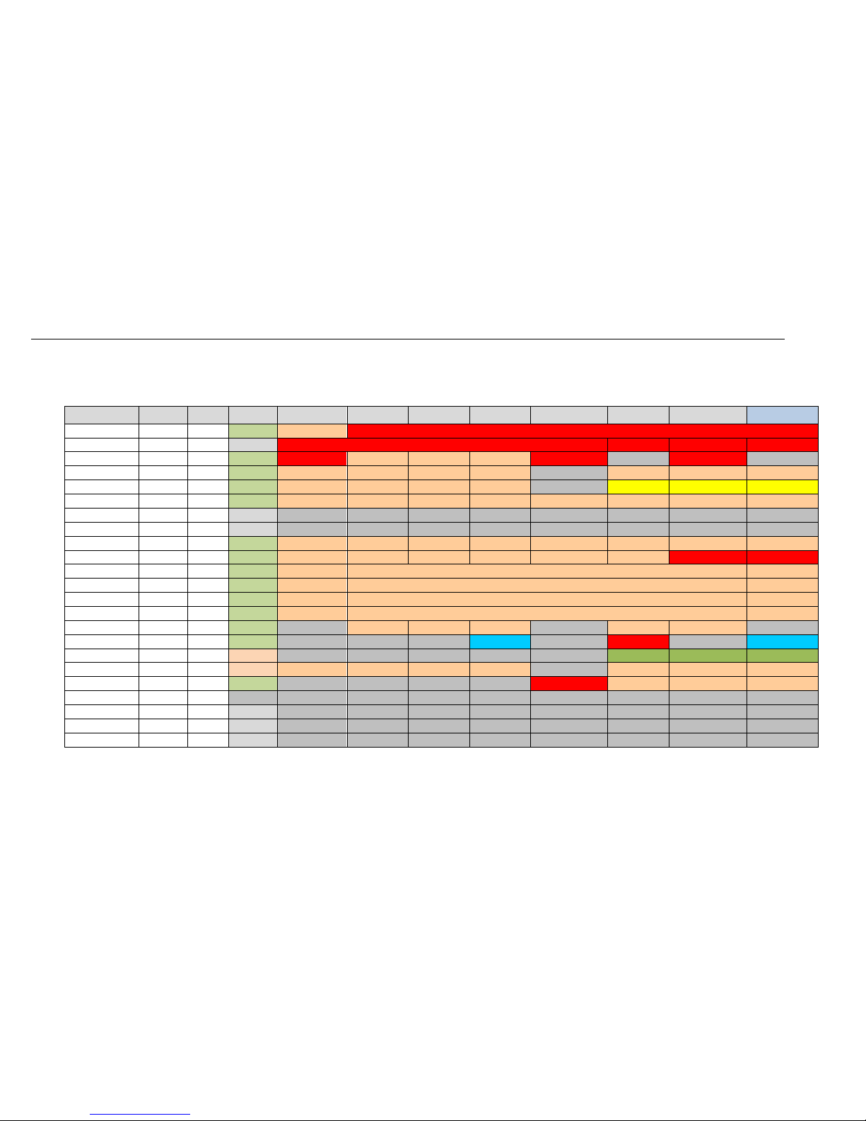
FPGA Registers
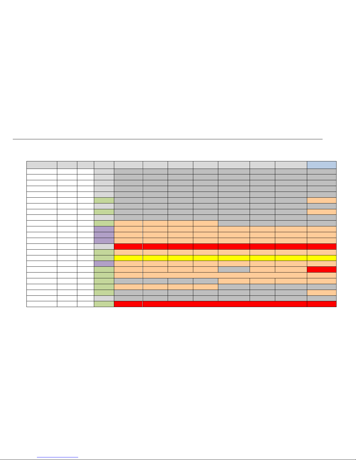
FPGA Registers
Table 3: FPGA I/O Map
Address Range Device Size
ISA BUS ADDRESSING AND LPC I/O AND MEMORY MAP
The FPGA implements an LPC-to-ISA bridge. The LPC bus only has the FPGA, the SCH3114,
and the TPM device on it. The TPM is a memory mapped device at base address 0xFED40000.
The SCH3114 uses I/O addresses 0x2E/0x2F for its index/data port. It also uses I/O space
0xC00-0xC7F for Runtime Registers. The FPGA uses I/O space 0xC80-0xCCF. The ISA bus
addressing can go up to 16Mbytes (24-bits of address). As such, the following will be the
allowed memory and I/O map for the ISA bus. Basically, all LPC I/O cycles that are unclaimed
by the FPGA will pass through to the ISA bus.
All LPC memory cycles below 16Mbytes will be passed through to the ISA bus. Note that the
actual cycles on the LPC bus are not known.
VL-EBX-38 Programmer’s Reference Manual 4
Page 10
FPGA Registers
0x2E-0x2F
SCH3114
Index/Data Port
0xC00-0xC7F
SCH3114
Runtime Registers
0xC80-0xCCF
FPGA Registers
80 Bytes
Depends on SoC LPC I/O traffic and
whether COM ports are enabled.
0x0 – 0xFFFFFF LPC memory cycles
ISA bus
Depends on SoC LPC memory traffic
0x1000000 and higher LPC memory
cycles
TPM is the only memory device on the
LPC bus
Table 4: ISA Bus I/O Map
Table 5: ISA Memory Map
Address Range Device Size
All Other LPC I/O Cycles ISA Bus
Address Range Device Size
Ignored by FPGA
5 VL-EBX-38 Programmer’s Reference Manual
Page 11
FPGA Registers
Register Access Key
WO
Write-Only
ROC
Read-Only and clear-to-0 after reading
If AUX_PSEN is a '0' in MISCSR1 (default setting) then thi s is the same as t he Platform reset. If AUX_PSEN is a
programmed to a '1' then it is the same as t he power-on reset POR.
FPGA Register Descriptions
R/W Read/Write
RO Read-only (status or reserved)
R/WC Read-status/Write-1-to-Clear
RSVD Reserved. Only write 0 to this bit; ignore all read values.
POR Power-on reset (only resets one tim e when input power comes on)
Platform Resets prior to the process or entering the S0 power state (i.e., at power-on and in sleep states)
resetSX
n/a Reset doesn't apply to status or reserved registers
Reset Key
6 VL-EBX-38 Programmer’s Reference Manual
Page 12
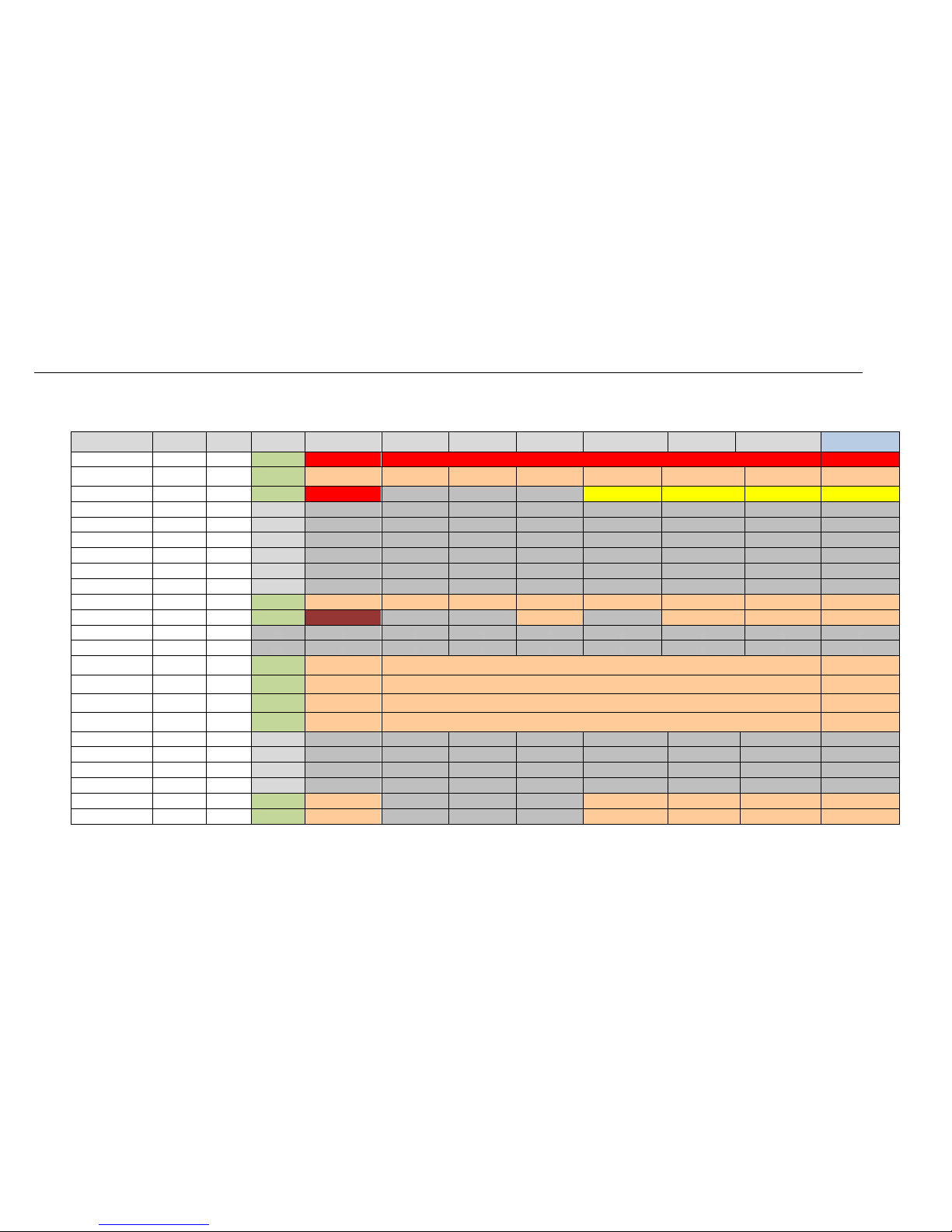
FPGA Registers
VL-EBX-38 Programmer’s Reference Manual 7
Identifier
I/O
Address
Offset
Reset
D7
D6
D5
D4
D3
D2
D1
D0
PCR
C80
0
Platform
PLED
PRODUCT_CODE
PSR
C81
1
n/a
REV_LEVEL
EXTEMP
CUSTOM
BETA
SCR
C82
2
Platform
BIOS_JMP
BIOS_OR
BIOS_SEL
LED_DEBUG
WORKVER
0
GPI_JMP 0 TIMR
C83
3
Platform
IRQEN
IRQSEL2
IRQSEL1
IRQSEL0
0
IMASK_TC5
IMASK_TC4
IMASK_TC3
TISR
C84
4
Platform
INTRTEST
TMRTEST
TMRIN4
TMRIN3
0
ISTAT_TC5
ISTAT_TC4
ISTAT_TC3
TCR
C85
5
Platform
TIM5GATE
TIM4GATE
TIM3GATE
TM45MODE
TM4CLKSEL
TM3CLKSEL
TMROCTST
TMRFULL
Reserved
C86
6
n/a 0 0 0 0 0 0 0 0
Reserved
C87
7
n/a 0 0 0 0 0 0 0 0
SPICONTROL
C88
8
Platform
CPOL
CPHA
SPILEN1
SPILEN0
MAN_SS
SS2
SS1
SS0
SPISTATUS
C89
9
Platform
IRQSEL1
IRQSEL0
SPICLK1
SPICLK0
HW_IRQ_EN
LSBIT_1ST
HW_INT
BUSY
SPIDATA0
C8A
A
Platform
msb
<============>
lsb
SPIDATA1
C8B
B
Platform
msb
<============>
lsb
SPIDATA2
C8C
C
Platform
msb
<============>
lsb
SPIDATA3
C8D
D
Platform
msb
<============>
lsb
SPIMISC
C8E
E
Platform 0 MUXSEL2
MUXSEL1
MUXSEL0
0
SERIRQEN
SPILB 0 ADM
C8F
F
Platform 0 0 0 DACLDA0
0
ADCBUSY0
0
ADCONVST0
MISCSR1
C90
10
POR 0 0 0 0 0 MINI1_PSDIS
AUX_PSEN
MINI0_PSDIS
MISCSR2
C91
11
POR
USB_HUBMODE
W_DISABLE
ETH1_OFF
ETH0_OFF
0
USB_HUBDIS
USB_PBDIS
USB_OBDIS
MISCSR3
C92
12
Platform 0 0 0 0
USB_PBOC
PBRESET
USB_PB_SMBEN
USB_OB_SMBEN
Reserved
C93
13
n/a 0 0 0 0 0 0 0 0
Reserved
C94
14
n/a 0 0 0 0 0 0 0 0
Reserved
C95
15
n/a 0 0 0 0 0 0 0 0
Reserved
C96
16
n/a 0 0 0 0 0 0 0 0
Page 13
FPGA Registers
8 VL-EBX-38 Programmer’s Reference Manual
Identifier
I/O
Address
Offset
Reset
D7
D6
D5
D4
D3
D2
D1
D0
Reserved
C97
17
n/a 0 0 0 0 0 0 0 0
Reserved
C98
18
n/a 0 0 0 0 0 0 0 0
Reserved
C99
19
n/a 0 0 0 0 0 0 0 0
Reserved
C9A
1A
n/a 0 0 0 0 0 0 0 0
Reserved
C9B
1B
n/a 0 0 0 0 0 0 0 0
DIOIMASK1
C9C
1C
Platform 0 0 0 0 0 0 0 IMASK_DIO1
DIOIMASK2
C9D
1D
n/a 0 0 0 0 0 0 0 0
DIOISTAT1
C9E
1E
Platform 0 0 0 0 0 0 0 ISTAT_DIO1
DIOISTAT2
C9F
1F
n/a 0 0 0 0 0 0 0 0
DIOCR
CA0
20
Platform
IRQEN
IRQSEL2
IRQSEL1
IRQSEL0 0 0 0 0
AUXDIR
CA1
21
resetSX
DIR_GPIO8
DIR_GPIO7
DIR_GPIO6
DIR_GPIO5
DIR_GPIO4
DIR_GPIO3
DIR_GPIO2
DIR_GPIO1
AUXPOL
CA2
22
resetSX
POL_GPIO8
POL_GPIO7
POL_GPIO6
POL_GPIO5
POL_GPIO4
POL_GPIO3
POL_GPIO2
POL_GPIO1
AUXOUT
CA3
23
resetSX
OUT_GPIO8
OUT_GPIO7
OUT_GPIO6
OUT_GPIO5
OUT_GPIO4
OUT_GPIO3
OUT_GPIO2
OUT_GPIO1
AUXIN
CA4
24
n/a
IN_GPIO8
IN_GPIO7
IN_GPIO6
IN_GPIO5
IN_GPIO4
IN_GPIO3
IN_GPIO2
IN_GPIO1
AUXIMASK
CA5
25
Platform
IMASK_GPIO8
IMASK_GPIO7
IMASK_GPIO6
IMASK_GPIO5
IMASK_GPIO4
IMASK_GPIO3
IMASK_GPIO2
IMASK_GPIO1
AUXISTAT
CA6
26
Platform
ISTAT_GPIO8
ISTAT_GPIO7
ISTAT_GPIO6
ISTAT_GPIO5
ISTAT_GPIO4
ISTAT_GPIO3
ISTAT_GPIO2
ISTAT_GPIO1
AUXMODE1
CA7
27
resetSX
MODE_GPIO8
MODE_GPIO7
MODE_GPIO6
MODE_GPIO5
MODE_GPIO4
MODE_GPIO3
MODE_GPIO2
MODE_GPIO1
WDT_CTL
CA8
28
Platform
IRQEN
IRQSEL2
IRQSEL1
IRQSEL0
0
RESET_EN
WDT_EN
WDT_STAT
WDT_VAL
CA9
29
Platform
msb
<============>
lsb
XCVRMODE
CAA
2A
Platform 0 0 0 0
COM4_MODE
COM3_MODE
COM2_MODE
COM1_MODE
AUXMODE2
CAB
2B
Platform
IRQEN
IRQSEL2
IRQSEL1
IRQSEL0 0 0 0 0
FANCON
CAC
2C
Platform 0 0 0 0 0 0 0 FAN_OFF
Reserved
CAD
2D
n/a 0 0 0 0 0 0 0 0
FANTACHLS
CAE
2E
Platform
msb
<============>
lsb
Page 14
FPGA Registers
9 VL-EBX-38 Programmer’s Reference Manual
Identifier
I/O
Address
Offset
Reset
D7
D6
D5
D4
D3
D2
D1
D0
FANTACHMS
CAF
2F
Platform
msb
<============>
lsb
TEMPICR
CB0
30
Platform
IRQEN
IRQSEL2
IRQSEL1
IRQSEL0
IMASK_BATTLO
W
IMASK_EVENT
IMASK_THERM
IMASK_ALERT
TEMPISTAT
CB1
31
Platform
BATTLOW 0 0 0 ISTAT_BATTLOW
ISTAT_EVENT
ISTAT_THERM
ISTAT_ALERT
Reserved
CB2
32
n/a 0 0 0 0 0 0 0 0
Reserved
CB3
33
n/a 0 0 0 0 0 0 0 0
Reserved
CB4
34
n/a 0 0 0 0 0 0 0 0
Reserved
CB5
35
n/a 0 0 0 0 0 0 0 0
UARTMODE1
CB6
36
n/a 0 0 0 0 0 0 0 0
UARTMODE2
CB7
37
n/a 0 0 0 0 0 0 0 0
ISACON1
CB8
38
Platform
ISA_IRQ11
ISA_IRQ10
ISA_IRQ9
ISA_IRQ7
ISA_IRQ6
ISA_IRQ5
ISA_IRQ4
ISA_IRQ3
ISACON2
CB9
39
Platform
ISA_ACCESS
0 0 ISA_16MODE
0
ISA_IRQ15
ISA_IRQ14
ISA_IRQ12
Reserved
CBA
3A
n/a 0 0 0 0 0 0 0 0
Reserved
CBB
3B
n/a 0 0 0 0 0 0 0 0
8254 Timers
Address 0
CBC
3C
Platform
msb
<============>
lsb
8254 Timers
Address 1
CBD
3D
Platform
msb
<============>
lsb
8254 Timers
Address 2
CBE
3E
Platform
msb
<============>
lsb
8254 Timers
Address 3
CBF
3F
Platform
msb
<============>
lsb
Reserved
CC0
40
n/a 0 0 0 0 0 0 0 0
Reserved
CC1
41
n/a 0 0 0 0 0 0 0 0
Reserved
CC2
42
n/a 0 0 0 0 0 0 0 0
Reserved
CC3
43
n/a 0 0 0 0 0 0 0 0
UART1CR
CC4
44
Platform
UART1_EN 0 0 0 UART1_BASE3
UART1_BASE2
UART1_BASE1
UART1_BASE0
UART2CR
CC5
45
Platform
UART2_EN 0 0 0 UART2_BASE3
UART2_BASE2
UART2_BASE1
UART2_BASE0
Page 15

FPGA Registers
10 VL-EBX-38 Programmer’s Reference Manual
Identifier
I/O
Address
Offset
Reset
D7
D6
D5
D4
D3
D2
D1
D0
UART3CR
CC6
46
Platform
UART3_EN 0 0 0 UART3_BASE3
UART3_BASE2
UART3_BASE1
UART3_BASE0
UART4CR
CC7
47
Platform
UART4_EN 0 0 0 UART4_BASE3
UART4_BASE2
UART4_BASE1
UART4_BASE0
Reserved
CC8
48
n/a 0 0 0 0 0 0 0 0
Reserved
CC9
49
n/a 0 0 0 0 0 0 0 0
Reserved
CCA
4A
n/a 0 0 0 0 0 0 0 0
Reserved
CCB
4B
n/a 0 0 0 0 0 0 0 0
Reserved
CCC
4C
n/a 0 0 0 0 0 0 0 0
Reserved
CCD
4D
n/a 0 0 0 0 0 0 0 0
Reserved
CCE
4E
n/a 0 0 0 0 0 0 0 0
Reserved
CCF
4F
n/a 0 0 0 0 0 0 0 0
Passed to ISA Bus
CD0-FFFF
--
--
Unknown
Page 16

1 – LED is on (can be used by sof tware)
6-0
PRODUCT_CODE
“0010111”
Product Code for the EBX-38 (0x17)
status bit (bit 0) i s set to ‘1’
1 – Extended Temp
0 – Production
Product Information Registers
This register drives the PLED on the paddleboard. It also provides read access to the product
code.
Table 6: PCR – Product Code and LED Register
Bit Identifier Access Default Description
7 PLED R/W 0
RO
Table 7: PSR – Product Status Register
Bit Identifier Access Default Description
7:3 REV_LEVEL[4:0]
RO
N/A
FPGA Registers
Drives the programm abl e LED on the paddleboard.
0 – LED is off (default)
Revision level of the PLD (incremented every FPGA release)
0 – Indicates production rel ease revision level when BETA
status bit (bit 0) i s set to ‘0’
1 – Indicates development release revision level when BETA
2 EXTEMP
1 CUSTOM
0 BETA
RO
RO
RO
N/A
N/A
N/A
Extended or Standard Temp Status (set via external resistor):
0 – Standard Temp
Custom or Standard Product Status (set in FPGA ):
0 – Standard Product
1 – Custom Product or P LD/ F PGA
Beta or Production Status (set in FPGA):
1 – Beta (or Debug)
VL-EBX-38 Programmer’s Reference Manual 11
Page 17

FPGA Registers
1 – BIOS Select will fol l ow the B I O S _SEL register setting
1 – LED is on (indicates FPGA is programmed by defaul t)
1 – FPGA is in a working stat e (not rel eased)
or may not be connected to a switch on the board.
0
0
Reserved. Writes are ignored; reads always return 0.
Hardware Reference Manual for more i nformation regarding the confi gurat i on switches.
BIOS AND JUMPER STATUS REGISTER
Table 8: SCR –Status/Control Register
Bit Identifier Access Default Description
7
6
5
4
3
BIOS_JMP
BIOS_OR
BIOS_SEL
LED_DEBUG
WORKVER
RO
R/W
R/W
R/W
RO
N/A
0
0
0
N/A
Status of the external BIOS switch (jumper):
1 – Primary BIOS sel ected
0 – Secondary BIOS selected
BIOS Switch (jumper) Override
0 – BIOS Select will f ol l ow the BI O S _JMP switch setting. (Note)
BIOS Select (see B I O S _OR):
1 – Primary BIOS sel ected
0 – Backup BIOS s el ected
Debug LED (controls the yellow LED):
0 – LED is off and follows it s pri mary function (MSATA_DAS)
Status used to indic at e that the FPGA is not of f i cially released
and is still in a working st at e.
0 – FPGA is released
RESERVED
2
GPI_JMP
1
RESERVED RO
Note: This corresponds to the setting of position 6 of the SW1 Configuration Switch block. Refer to the EBX-38
RO
RO
N/A Reserved. Writes are ignored; reads always return 0.
N/A Status of the GPI Jumper (switch):
0 – Switch is Off
1 – Switch is On
FYI – this is a tradit i onal “j umper” that goes to the FPGA . It may
12 VL-EBX-38 Programmer’s Reference Manual
Page 18

FPGA Registers
1 – Interrupts enabled
111 – IRQ11
1 – Interrupt enabled
1 – Interrupt enabled
TIMER REGISTERS
The FPGA implements an 8254-compatible timer/counter that includes three 16-bit timers.
Table 9: TICR – 8254 Timer Interrupt Mask Register
Bit Identifier Access Default Description
8254 Timer interrupt enable/dis abl e:
7 IRQEN
6-4 IRQSEL(2:0)
R/W
R/W
0
000
0 – Interrupts disabled
8254 Timer interrupt IRQ select in LPC SERIRQ:
000 – IRQ3
001 – IRQ4
010 – IRQ5
011 – IRQ10
100 – IRQ6
101 – IRQ7
110 – IRQ9
3 RESERVED
2 IMSK_TC5
1 IMSK_TC4
0 IMSK_TC3
RO
R/W
R/W
R/W
0 Reserved. Writes are ignored; reads al ways return 0.
8254 timer #5 interrupt mask:
0
0 – Interrupt disabled
8254 timer #4 interrupt mask:
0
0 – Interrupt disabled
1 – Interrupt enabled
8254 timer #3 interrupt mask:
0
0 – Interrupt disabled
VL-EBX-38 Programmer’s Reference Manual 13
Page 19

FPGA Registers
to be set for this)
1 – asserted
1 – asserted
3
RESERVED
0
Reserved. Writes are ignored; reads always return 0.
1 level
1 level
1 level
Table 10: TISR – 8254 Timer Interrupt Status Register
Bit Identifier Access Default Description
7 INTRTEST
6 TMRTEST
5 TMRIN4
4 TMRIN3
R/W
R/W
R/W
R/W
Debug/Test Only -- 8254 Timer I nterrupt Test (test mode only):
0 – No test interrupt: M ust be set to 0 for normal operation.
0
1 – If IRQEN is a 1 then an int errupt will assert in the selected
IRQ in the LPC SERIRQ st ream (no timer interrupt mask needs
Debug/Test Only -- 8254 Timer Test Mode:
0 – Normal operation: Must be set to 0 for normal operation.
1 – Timer test mode. In test mode t he OCT C3, OCT C4 (and
0
OCTC5 if ever implem ented) outputs are set to Hi-Z and the
ICTC3, ICTC4 timer inputs are ignored. This is basi cally the
internal timer test mode not requiring external signals.
Debug/Test Only -- 8254 Timer #4 t est signal. When TMRTEST
= 1 this signal is used for the timer input cont rol i nstead of the
external ICTC4 signal. When INTRTEST = 0 this is i gnored.
0
0 – deasserted
Debug/Test Only -- 8254 Timer #3 t est signal. When TMRTEST
= 1 this signal is used for the timer input cont rol i nstead of the
external ICTC3 signal. W hen INTRTEST = 0 this is i gnored.
0
0 – deasserted
2 ISTAT_TC5
1 ISTAT_TC4
0 ISTAT_TC3
RO
RW/C
RW/C
RW/C
N/A
N/A
N/A
Status for the 8254 Timer #5 output (terminal count ) interrupt
when read. This bit is read-status and a write-1-to-clear.
0 – Timer output (term i nal count) has not transitioned from 0 to
a 1 level
1 – Timer output (term i nal count) has transitioned from a 0 to a
Status for the 8254 Timer #4 output (terminal count ) interrupt
when read. This bit is read-status and a write-1-to-clear.
0 – Timer output (term i nal count) has not transitioned from 0 to
a 1 level
1 – Timer output (term i nal count) has transitioned from a 0 to a
Status for the 8254 Timer #3 output (terminal count ) interrupt
when read. This bit is read-status and a write-1-to-clear.
0 – Timer output (term i nal count) has not transitioned from 0 to
a 1 level
1 – Timer output (term i nal count) has transitioned from a 0 to a
14 VL-EBX-38 Programmer’s Reference Manual
Page 20

Table 11: TCR – 8254 Timer Control Register
internal clocking.
internal clocking
Timer #5 is always on internal cl ock if configured as a 16-bit clock
operation.
GPIOs to use for Timer signals (MODE_GPIO[8:3] must each be a ‘ 1’
Bit Identifier Access Default Description
Debug/Test Only: Controls the “gate” signal on 8254 timer #5 when not
using an external gate signal:
7 TMR5GATE
6 TMR4GATE
5 TMR3GATE
R/W
R/W
R/W
0 – Gate on signal GCTC5 is disabl ed
0
1 – Gate on signal GCTC5 is enabled
Always set to 0 when configuring timer modes except when TMRFULL
is ‘0’ and then it should be set to ‘1’ and not changed unless using
Controls the “gate” signal on 8254 timer #4 when not using an external
gate signal:
0 – Gate on signal GCTC4 is disabl ed
0
1 – Gate on signal GCTC4 is enabled
Always set to 0 when configuring timer modes except when TMRFULL
is ‘0’ and then it should be set to ‘1’ and not changed unless using
internal clocking
Controls the “gate” signal on 8254 timer #3 when not using an external
gate signal:
0 – Gate on signal GCTC3 is disabl ed
0
1 – Gate on signal GCTC3 is enabled
Always set to 0 when configuring timer modes except when TMRFULL
is ‘0’ and then it should be set to ‘1’ and not changed unless using
FPGA Registers
4 TM45MODE
3 TM4CLKSEL
2 TM3CLKSEL
1 TMROCTST
0 TMRFULL
R/W
R/W
R/W
R/W
R/W
Mode to set timers #4 and #5 i n:
0 – Timer #4 and #5 form one 32-bit timer controlled by timer #1 signals
1 – Timer #4 and Timer #5 are separate 16-bit timers with their own
0
control signals.
Almost always used in 32-bit mode especially when TMRFULL is a ‘0’
(the 16-bit timer #5 is of l i mited use)
Timer #4 Clock Selec t :
0 – Use internal 4.125 MHz clock (derived from PCI cloc k)
0
1 – Use external ICTC4
Timer #3 Clock Selec t :
0 – Use internal 4.125 MHz clock (deri ved f rom PCI clock)
0
1 – Use external ICTC3 assigned to Digital I/O
Debug/Test Only: Used to derive OCTCx outputs with TMRxGATE
0
signals for continuit y t esting only: Must be set to 0 for no r m al
in AUXMODE1 Register to use all the external timer signals).:
0 – 4-wire timers (GPIO4 and GPI O 3 external gat e signals not used)
are external Timer control signals
1 – 8-wire timers; six GPIOs (GPIO8 – GPIO3) are external Timer
control signals
0
Note: Since the gates-controls are not connected t o GPIOs when
TMRFULL is a ‘0’ the TMRxGATE gate controls i n t hi s register are used
so they need to be set to ‘1’ and shoul d not be toggled during operation
with external timers (since there i s no continuous clock to synchronize
them to) but can be toggled if using the internal cloc k . If you need
gating in external modes then you really need to s et T MRFULL t o a ‘ 1’ .
VL-EBX-38 Programmer’s Reference Manual 15
Page 21

FPGA Registers
SPI clock polarity – Set s the SCLK idle state.
1 – SCLK idles high
1 – Data is read on falling edge
11 – 32-bit
bits SS[2:0]
111 – DAC (digital to analog output c onvers i on devi ce)
SPI CONTROL REGISTERS
These are placed at the traditional offset 0x8 location. On-board SPI interface devices (DIOs,
ADC, and DAC for the EBX-38) and off-board SPX interface devices use this interface. The
EBX-38 is using the standard 2mm 2x7 pin header/14-pin SPX connector and can support up to
four devices and an interrupt input.
SPICONTROL
Table 12: SPI Interface Control Register
Bit Identifier Access Default Description
7 CPOL
6 CPHA
5-4
SPILEN(1:0)
3 MAN_SS
2-0 SS(2:0)
R/W 0
R/W 0
R/W 00
R/W 0
R/W 000
0 – SCLK idles low
SPI clock phase – Sets the SCLK edge on which valid data will be read.
0 – Data is read on rising edge
Determines the SPI frame length. This s el ection works in manual and
auto slave select m odes.
00 – 8-bit
01 – 16-bit
10 – 24-bit
Determines whether the slave select lines are asserted through the
user software or are automatical l y as serted by a write to SPIDATA3.
0 - The slave select operates aut omatically
1 - The slave select line is controlled manually through S PICONTROL
SPI Slave Device Select i on:
000 – None
001 – SS0# (SPX slave device 0)
010 – SS1# (SPX slave device 1)
011 – SS2# (SPX slave device 2)
100 – SS3# (SPX slave device 3)
101 – ADC (analog input to digital conversion device)
110 – DIO (two digital I/O devices , di fferentiated by SPI address i ng)
16 VL-EBX-38 Programmer’s Reference Manual
Page 22
FPGA Registers
of eight interrupts.
1 - The IRQ can be asserted
1 - Data is right-shift ed (LS B first)
interrupt is no longer present.
SPISTATUS
The SPX interrupt is not connected on this product. The control bits and status associated are
still defined in the register set but the SPX interrupt will always be de-asserted.
Table 13: SPI Interface Status Register
Bits Identifier
7-6
IRQSEL[1:0]
5-4
SPICLK(1:0)
3
HW_IRQ_EN
2
LSBIT_1ST
Access Default
R/W 00
R/W 00
R/W 0
R/W 0
Description
The SPX interrupt is not connect ed on t hi s product (always de-asserted).
Selects which IRQ will be enabled if HW_IRQ_EN = 1. Interrupts are not
used on this board, so this j ust becomes a read/write non-func tional field.
00 – IRQ3
01 – IRQ4
10 – IRQ5
11 – IRQ10
Note: These are the first four interrupts in the “usual” LP C SERIRQ group
Selects one of four SCLK f requencies. This is based on a 33 MHz LPC
clock.
00 – 1.03125 MHz (33 MHz/32)
01 – 2.0625 MHz (33 MHz/16)
10 – 4.125 MHz (33 MHz/8)
11 – 8.25 MHz (33 MHz/4)
The SPX interrupt is not connect ed on t hi s product (always de-asserted).
This enables the select ed IRQ to be activated by a SPI devic e that is
configured to use its interrupt capability.
0 - IRQs are disabled for SPI operations.
Controls the SPI shif t direction from the S PIDATA(x) registers.
0 - Data is left-shifted (MSB first).
SPX interrupt is not connected on t hi s product (always de-asserted).
Status flag which indicat es when the hardware SPX signal SINT# is
asserted.
1 HW_INT RO 0
0 BUSY
RO
N/A
0 - The hardware interrupt SINT# is de-asserted.
1 - An interrupt is present on SINT#
If HW_IRQ_EN= 1, the selected IRQ will also be asserted by the hardware
interrupt. HW_I NT i s read-only and is cleared when the external hardware
Status flag which indicat es when an SPI transaction is underway. I2C is so
slow that there is no reason to ever poll t hi s.
0 - The SPI bus is idl e.
1 - SCLK is clocking data i n/ out of the SPIDATA(x) registers (that is, busy)
VL-EBX-38 Programmer’s Reference Manual 17
Page 23

FPGA Registers
SPI DATA REGISTERS
There are four data registers used on the SPI interface. How many are used depends on the
device being communicated with. SPIDATA0 is typically the least significant byte and
SPIDATA3 is the most significant byte. Any write to the most significant byte SPIDATA3
initiates the SCLK and, depending on the MAN_SS state, will assert a slave select to begin an
SPI bus transaction.
Data is sent according to the LSBIT_1ST setting. When LSBIT_1ST = 0, the MSbit of
SPIDATA3 is sent first and received data will be shifted in the LSbit of the selected frame size
determined by SPILEN1 and SPILEN0. When LSBIT_1ST = 1, the LSbit of the selected frame
size is sent first and the received data will be shifted in the MSbit of SPIDATA3.
SPIDATA0 (Least Si gnificant Byte)
D7 D6 D5 D4 D3 D2 D1 D0
MSB LSB
SPIDATA1
D7 D6 D5 D4 D3 D2 D1 D0
MSB LSB
SPIDATA2
D7 D6 D5 D4 D3 D2 D1 D0
MSB LSB
SPIDATA3 (Most Significant Byte) [Cycle Trigger Register]
D7 D6 D5 D4 D3 D2 D1 D0
MSB LSB
18 VL-EBX-38 Programmer’s Reference Manual
Page 24

FPGA Registers
7
Reserved
0
Reserved. Writes are ignored; reads always return 0.
mSATA/PCIe Mux selection for Minicard slot (and 2nd SATA connector):
to the SATA connector.
3
Reserved
0
Reserved. Writes are ignored; reads always return 0.
Debug/Test Only: Used to loop SPI output data back to t he i nput (debug/test
1 – Loop SPI output data back to the SPI input data (data out put still active)
SPI DEBUG CONTROL REGISTER AND MSATA/PCIE SELECT CONTROL REGISTER
This register is only used to set an SPI loopback (debug/test only) but is also used for the
mSATA/PCIe Minicard Mux select.
Table 14: SPI – SPI Debug Control Register
Bit Identifier
MUXSEL
6-4
(2:0)
2
SERIRQEN
1 SPILB
Access Default
RO
R/W
RO
R/W
R/W
Description
• 000 – Selects P CI e Mode for the EBX-38. This is an Intel-Mode that i s
reliable for PCIe Minicard but not f or mSATA modules that inadvertently
ground this signal.
• 001 – Use only Pin 51 (PRE S_DISABLE2#). This is the default method
and is defined in the Draft m SATA spec but some Minicards use it as a
second wireless disable.
• 010 – Use either Pi n 43 or P i n 51. Same as 000 for EBX-38.
000
• 011 – Force PCIe mode on the Minicard
• 100 – Force mSATA mode on the Minicard.
• 101 – Undefined (same as 000)
• 110 – Undefined (same as 000)
• 111 – Undefined (same as 000)
Note: When the Mini card uses PCIe, the SATA channel autom atically switches
When an IRQ is as signed a slot in the SERIRQ, i t will drive the slot with the
interrupt state, but t hi s bi t must be set to a ‘ 1’ t o do that.
0 – Slots assigned to SERIRQ are not driven (available for other devices ).
1 – Slots assigned to SERIRQ are driven with their current interrupt state (which
0
is low since interrupts are high-true).
This is because the default int errupt settings in this FPGA can conflict with
other interrupts if the Vers aAPI is not being used (for exampl e, console redirect
using IRQ3).
mode).
0
0 – Normal operation
0
RESERVED
RO
0 Reserved. Writes are ignored; reads always return 0.
VL-EBX-38 Programmer’s Reference Manual 19
Page 25

FPGA Registers
Bits
Identifier
Access
Default
7:5
RESERVED
000
Reserved – Writes are i gnored. Reads always return 000
4
DACLDA0
0
This is the DAC load enable signal .
3
RESERVED
0
Reserved – Writes are i gnored. Reads always return 0
processing a conversion request .
1
RESERVED
0
Reserved – Writes are i gnored. Reads always return 0
0
ADCONVST0
0
This is the ADC conversion start signal.
ADM – A/D AND D/A SPI DEVICE CONTROL REGISTER
This register is used to start an Analog to Digital Conversion or load a Digital to Analog value
load via the SPI interface to the A/D and D/A devices. The bit positions match the similar
register in the EBX-41, except there are no optional controls for a second ADC and/or DAC.
Reset type is Platform.
2 ADCBUSY0
RO
WO
RO
RO
RO
WO
Description
0
This is the ADC BUSY signal. It will be low when the ADC is
20 VL-EBX-38 Programmer’s Reference Manual
Page 26

FPGA Registers
sophisticated as nec essary.
powered down in sleep modes and the configuration will remain
MISCELLANEOUS FPGA REGISTERS
MISCR1 – Miscellaneous Contr ol Register #1
This is a register in the always-on power well of the FPGA. It holds its state during sleep modes
and can only be reset by a power cycle. This is a placeholder register for features like pushing the
power-button and also for software initiated resets should those be needed. This register is only
reset by the main power-on reset since it must maintain its state in Sleep modes (for example,
S3).
Table 15: MISCR1 – Misc. Control Register #1
Bits Identifier Access Default Description
7-3 RESERVED RO
2 MINI1_PSDIS R/W
0s Reserved. Writes are ignored; reads always return 0.
Minicard1 3.3V Power Disable
0 – Minicard1 3.3V power stays on always (this is normally how
Minicards operate if they support any WAKE events)
1 – Minicard1 3.3V power will be turned off when not in S0 (in sleep
modes).
The Minicard1 3.3V power switch is control l ed by t he “OR” of the
0
S0 power control signal and the inverse of MINI1_PSDIS
Note: Either always leave on or turn it of f One Time. Otherwise
there could be issues. A res et is always a good idea after changing
the state on power since the BIOS/OS may get confus ed since
these are like hot-plug events. E ntry/exit on this can be made more
Auxiliary Power Supply enable (for Digital I/O and AUX GPIO
Power)
1 AUX_PSEN R/W
0 MINI0_PSDIS R/W
0 – The Digital I/O devices and A UX GPIO pul l -ups will be powered
0
down in sleep modes (only power in S0)
1 – The Digital I/O devices and A UX GPIO pul l -ups will not be
Minicard0 3.3V Power Disable
0 – Minicard0 3.3V power stays on always (this is normally how
Minicards operate if they support any WAKE events)
1 – Minicard0 3.3V power will be turned off when not in S0 (in sleep
modes).
The Minicard0 3.3V power switch is control l ed by t he “OR” of the
0
S0 power control signal and the inverse of MINI0_PSDIS
Note: Either always leave on or turn it of f One Time. Otherwise
there could be issues. A reset is always a good idea after changing
the state on power since the BIOS/OS may get confus ed since
these are like hot-plug events. E ntry/exit on this can be made more
sophisticated as nec essary.
MISCR2 – Miscellaneous Contr ol Register #2
This is a register in the always-on power well of the FPGA. It holds its state during sleep modes
and can only be reset by a power cycle. It is primarily used for control signals for the alwayspowered Ethernet controllers and the USB hubs. This register is only reset by the main power-on
reset since it must maintain its state in sleep modes (for example, S3).
VL-EBX-38 Programmer’s Reference Manual 21
Page 27

FPGA Registers
entering all sleep modes). USB ports cannot be used to wake-up
1 – Ethernet controller is di s abl ed (O f f)
1 – Ethernet controller is di s abl ed (O f f)
3
Reserved
0
Reserved – Writes are i gnored. Reads always return 0.
1 – USB251xB Hubs are in Reset
then a 0
at least 1 ms in bet ween
Table 16: MISCSR2 – Misc. Control Register #2
Bit
Identifier
7
6 W_DISABLE
5 ETHOFF1
4 ETHOFF0
USB_HUBMODE
Access Default
R/W
R/W
R/W
R/W
Description
Determines whether the hub resets onl y onc e (to support wake-up from
sleep modes on USB ports ) or resets every time it enters sleep modes
using the platform res et :
0
0 – USB hub is reset once at power on. Use USB _HUB DI S to manually
control the reset if nec es sary. This supports USB wake-up modes
1 – USB hub is reset by platform reset every time (will be reset when
Used to control the W_DISABLE (Wireless Disable) s i gnal goi ng t o the
PCIe Minicard:
0 – W_DISAB LE signal is not assert ed (E nabl ed)
0
1 – W_DISAB LE signal is asserted (Disabled)
Note: There are other control sourc es that can be configured to c ontrol
this signal and if enabled the control becomes t he “O R” of al l sources
Used to disable the Ethernet controller #1 (controls the ETH_OFF#
input to the I210-IT):
0
0 – Ethernet controller is enabl ed (On)
Used to disable the Ethernet controller #0 (controls the ETH_OFF#
input to the I210-IT):
0
0 – Ethernet controller is enabl ed (On)
2 USB_HUBDIS
1 USB_PBDIS
0 USB_OBDIS
RO
R/W
R/W
R/W
Control the reset on the USB251xB Hubs.
0’s
0 – USB251xB Hubs are Enabled (reset released)
Disable control for the paddleboard USB port VBUS power switches
(there are two power-switches but they have a common power enable
and overcurrent status)
0 – VBUS power switches are enabled
0
1 – VBUS power switched are disabled.
Note: The power switches latch-of f in overcurrent and can only be re-
enabled by a power-cycle or by setting this bit to a 1, wait >1 ms, and
Disable control for the on-board USB port VBUS power switches (there
are two with a common overcurrent):
0 – VBUS power switches are enabled
0
1 – VBUS power switched are disabled.
Note: The power switches latch-of f in overcurrent and can only be re-
enabled by a power-cycle of by setting this bit to a 1 and then a 0 with
22 VL-EBX-38 Programmer’s Reference Manual
Page 28

FPGA Registers
7-4
Reserved
0000
Reserved. Writes are ignored; reads always return 0.
1 – Overcurrent is asserted (power switch i s off)
so it is somewhat “write-only”.
(for SMBus connection)
MISCR3 – Miscellaneous Contr ol Register #3
This register has miscellaneous control and status signals. The USB paddleboard power switch
overcurrent status, the push-button reset signal control, and the SMBus enables for the USB Hub
devices reside here.
Table 17: MISCR3 – Misc. Control Register #3
Bits Identifier Access Default Description
RO
Reads the overcurrent status f or the USB paddleboard
power switches (there are two power switches for the four
3 USB_PBOC
2 PBRESET
RO
R/W
N/A
---
ports but they have a comm on overcurrent status).
0 – Overcurrent is not ass ert ed (power switc h i s on)
When written to, t hi s will do the same thing as pus hi ng the
reset button, which could be useful for a software-initiated
watchdog.
0 – No action
1 – Activate the reset push-button
Note: Because this generat es a reset that will reset thi s
register, it isn’t li kely a value of a ‘1’ can ever be read-back,
1 USB_PB_SMBEN
0 USB_OB_SMBEN
R/W
R/W
0
0
USB Paddle-Board Hub (USB2514B) SMBus enable signal
USB On-Board Hub (USB2513B) SMBus enable signal (for
SMBus connection) – when this is on USB_PB_SMBEN will
be forced off by the FPGA regardles s of the setting in its
register since the parts share the same address and would
cause a conflict if both were enabled during an access
intended for only one of them.
VL-EBX-38 Programmer’s Reference Manual 23
Page 29

FPGA Registers
7-1
RESERVED
Reserved – Writes are i gnored. Reads always return 0’s
Bits
Identifier
Access
Default
Description
7-1
RESERVED
0’s
Reserved – Writes are i gnored. Reads always return 0’s
N/A
from low-to-high on the shared interrupt input.
DIOIMASK1 – Digital I/O Interrupt Mask Register
This is the interrupt mask register for the digital I/Os (the two SPI devices share a common
interrupt input).
Reset type is Platform.
Table 18: DIOIMASK1 – Digital I/O 8-1 Interrupt Mask Register
Bits Identifier Access Default Description
0 IMASK_DIO1
DIOISTAT1 – Digital I/O Interrupt Status Register
Reset type is Platform
RO 0’s
R/W 0
Digital I/O Interrupt Mask :
0 – Interrupt disabled
1 – Interrupt enabled.
Table 19: DIOISTAT1 – Digital I/O 8-1 Interrupt Status Register
RO
0 ISTAT_DIO1
RW/C
DIOx interrupt status. A read ret urns the interrupt status . Writing a ‘1’
will clear the interrupt status. This bit is set to a ‘1’ on a t rans i tion
24 VL-EBX-38 Programmer’s Reference Manual
Page 30

DIOCR – DIGITAL I/O CONTROL REGISTER
1 – Interrupts enabled.
FYI – same values are other products.
3-0
RESERVED
0’s
Reserved – Writes are i gnored. Reads always return 0
One interrupt can be generated for the 32 SPI based digital I/Os.
Reset type is Platform
Table 20: DIOCR – Digital I/O Control Register
Bits Identifier Access Default Description
DIO Interrupt Enable/Disabl e:
7 IRQEN
6-4 IRQSEL(2:0)
R/W
R/W
0
000
0 – Interrupts disabled
DIO Interrupt IRQ Select i n LP C S ERIRQ:
000 – IRQ3
001 – IRQ4
010 – IRQ5
011 – IRQ10
100 – IRQ6
101 – IRQ7
110 – IRQ9
111 – IRQ11
FPGA Registers
RO
VL-EBX-38 Programmer’s Reference Manual 25
Page 31

FPGA Registers
1 – Output
edge used.
1 – Asserts the output (1 i f polarity not-inverted, 0 if inverted)
AUXDIR – AUX GPIO Direction Control Register
This register controls the direction of the eight AUX GPIO signals.
This reset depends on the state of the AUX_PSEN signal. If AUX_PSEN is a ‘0’ then the reset is
the power-on and Platform Reset. If AUX_PSEN is a ‘1’ then this register is only reset at poweron.
Table 21: AUXDIR – AUX GPIO Direction Control Register
Bit Identifier Access Default Description
7-0 DIR_GPIO[8:1]
AUXPOL – AUX GPIO Polarity Control Register
This register controls the polarity of the eight AUX GPIO signals.
This reset depends on the state of the AUX_PSEN signal. If AUX_PSEN is a ‘0’ then the reset is
the power-on and Platform Reset. If AUX_PSEN is a ‘1’ then this register is only reset at poweron.
R/W
Sets the direction of the AUX GPIOx lines. For each bit:
0
0 – Input
Table 22: AUXPOL – AUX GPIO Polarity Control Register
Bits Identifier Access Default Description
Sets the polarity of the A UX GPIOx lines . F or each bit:
0 – No inversion
7-0 POL_GPIO[8:1]
R/W
0
1 – Invert
Note: This impac ts the polarity as well as the int errupt status
AUXOUT – AUX GPIO Output Control Regi st er
This register sets the AUX GPIO output value. This value will only set the actual output if the
GPIO direction is set as an output. Reading this register does not return the actual input value of
the GPIO (use the AUXIN register for that). As such, this register can actually be used to detect
input/output conflicts.
This reset depends on the state of the AUX_PSEN signal. If AUX_PSEN is a ‘0’ then the reset is
the power-on and Platform Reset. If AUX_PSEN is a ‘1’ then this register is only reset at poweron.
Table 23: AUXOUT – AUX GPIO Output Control Register
Bits Identifier Access Default Description
Sets the AUX GPIOx output values. For eac h bi t :
7-0 OUT_GPIO[8:1]
R/W
0 – De-asserts the output (0 if polarity not-inverted, 1 if i nvert ed)
0
26 VL-EBX-38 Programmer’s Reference Manual
Page 32

FPGA Registers
de-asserted if polarity inverted
1 – Interrupt enabled
(POL_DIOx=0) or high-to-low (POL_DIOx=1).
AUXIN – AUX GPIO I/O Input Status Register
This registers sets the AUX GPIO input value. It will read the input value regardless of the
setting on the direction (that is, it always reads the input). This reads the actual state of the GPIO
pin into the part.
Table 24: AUXIN – AUX GPIO Input Status Register
Bits Identifier Access Default Description
Reads the GPIOx input status. For each bit:
7-0 IN_GPIOIO[8:1]
RO
N/A
0 – Input de-asserted if polarit y not -inverted;
asserted if polarity inverted
1 Input asserted if polarit y not-inverted;
AUXIMASK – AUX GPIO Interrupt Mask Register
This is the interrupt mask registers for the AUX GPIOs and the interrupt enable selection. The
reset type is Platform Reset because interrupts always have to be setup after exiting sleep states.
Table 25: AUXICR – AUX GPIO Interrupt Mask Register
Bits Identifier Access Default Description
GPIOx interrupt mask. For each bit:
7-0
IMASK_GPIO[8:1]
R/W
0
0 – Interrupt disabled
AUXISTAT – AUX GPIO I/O Interrupt Status Register
Table 26: AUXISTAT – AUX GPIO Interrupt Status Register
Bits Identifier Access Default Description
GPIOx interrupt status. A read ret urns the interrupt status. Writing
7-0
ISTAT_GPIO[8:1]
RW/C
N/A
a ‘1’ clears the interrupt s tatus.
This bit is set t o a ‘ 1’ on a t ransition from low-to-high
VL-EBX-38 Programmer’s Reference Manual 27
Page 33

FPGA Registers
1 – ICTC3 (Input clock f or T i mer 3)
1 – ICTC4 (Input clock f or T i mer 4)
1 – OCTC4 (Output for Timer 4)
1 – GCTC3 (Input gate for Timer 3)
1 – GCTC4 (Input gate for Timer 4)
1 – SLEEP# (Output, ac t i ve l ow SLEE P now signal)
AUXMODE1– AUX I/O Mode Register #1
These two registers selected the mode on each AUX GPIO. This reset depends on the state of the
AUX_PSEN signal. If AUX_PSEN is a ‘0’ then the reset is the power-on and Platform Reset. If
AUX_PSEN is a ‘1’ then this register is only reset at power-on.
Table 27: AUXMODE1 – AUX I/O Mode Register
Bit Identifier Access Default Description
7 MODE_GPIO8
6 MODE_GPIO7
5 MODE_GPIO6
4 MODE_GPIO5
R/W
R/W
R/W
R/W
GPIO 8 Mode:
0
0 – GPIO (I/O)
GPIO 7 Mode:
0
0 – GPIO (I/O)
GPIO 6 Mode:
0
0 – GPIO (I/O)
1 – OCTC3 (Output for Timer 3)
GPIO 5 Mode:
0
0 – GPIO (I/O)
3 MODE_GPIO4
2 MODE_GPIO3
1 MODE_GPIO2
0 MODE_GPIO1
R/W
R/W
R/W
R/W
GPIO 4 Mode:
0
0 – GPIO (I/O)
GPIO 3 Mode:
0
0 – GPIO (I/O)
GPIO 2 Mode:
0
0 – GPIO (I/O)
GPIO 1 Mode:
0
0 – GPIO (I/O)
1 – WAKE# (I nput, active low WA K E up signal)
28 VL-EBX-38 Programmer’s Reference Manual
Page 34

WDT_CTL – Watchdog Control Register
1 – Interrupts enabled
111 – IRQ11
1 – Board will be reset if the Watchdog “fires”
Note:
a reset occurs
Reset type is Platform.
Table 28: WDT_CTL – Watchdog Control Register
Bits Identifier Access Default Description
Watchdog int errupt enable/disable:
7 IRQEN
6-4 IRQSEL(2:0)
R/W
R/W
0
000
0 – Interrupts disabled
Watchdog interrupt I RQ select in LPC SERIRQ:
000 – IRQ3
001 – IRQ4
010 – IRQ5
011 – IRQ10
100 – IRQ6
101 – IRQ7
110 – IRQ9
FPGA Registers
3 Reserved
2 RESET_EN
1 WDT_EN
0 WDT_STAT
RO
R/W
R/W
RO
0 Reserved. Writes are ignored; reads al ways return 0.
Enable the Watchdog to assert the push-butt on reset if it “fires”.
0
0 – Watchdog will not reset the board
Watchdog Enable:
0 – Watchdog is disabled
0
1 – Watchdog is enabled
The WDT_VAL regis ter must be set before enabl i ng.
Watchdog St at us:
0 – Watchdog disabled or watchdog has not “fired”
1 – Watchdog f i red.
Note: Once set to a ‘1’, it will remain so until any of the following
0
occurs:
• the WDT_VAL register is written to
• the WDT_EN is disabled
•
VL-EBX-38 Programmer’s Reference Manual 29
Page 35

FPGA Registers
Bits
Identifier
Access
Default
Description
set to a ‘1’.
7-4
Reserved
0s
Reserved. Writes are ignored; reads always return 0.
1 – RS422/485
1 – RS422/485
WDT_VAL – Watchdog Value Register
This register sets the number of seconds for a Watchdog prior to enabling the watchdog. By
writing this value, the watchdog can be prevented from “firing”. A watchdog fires whenever this
registers value is all 0s, so it must be set to a non-zero value before enabling the watchdog to
prevent an immediate “firing”.
Reset type is Platform.
The value written should always be 1 greater than the desired timeout value due to a 0-1 second
“tick” error band (values written should range from 2-255 because a 1 could cause an immediate
trigger); that is, the actual timeout is WDT_VAL seconds with a -1 second to 0 second error
band.
Table 29: WDT_VAL – Watchdog Control Register
7-0 WDT_VAL(7:0)
R/W
0x00
Number of seconds before the Watchdog fires. By default, it is
set to zero which results in an immediate watchdog if WDT_EN is
XCVRMODE – COM Transceiver Mode Register
Sets the RS232 vs RS422/485 mode on the COM port Transceivers. These drive the UART_SEL
signals from the FPGA to the Transceivers.
Reset type is Platform.
Note: The values shown are for the default BIOS configuration.
Table 30: XCVRMODE – COM Transceiver Mode Register
Bits Identifier Access Default Description
RO
COM4 Transceiver mode:
3 COM4_MODE
2 COM3_MODE
R/W
R/W
0
0 – RS232
1 – RS422/485
COM3 Transceiver mode:
0
0 – RS232
1 COM2_MODE
0 COM1_MODE
30 VL-EBX-38 Programmer’s Reference Manual
R/W
R/W
COM2 Transceiver mode:
0
0 – RS232
1 – RS422/485
COM1 Transceiver mode:
0
0 – RS232
Page 36

AUXMODE2– AUX I/O Mode Register #2
1 – Interrupts enabled
111 – IRQ11
3-0
Reserved
0000
Reserved. Writes are ignored; reads always return 0.
Note: The BIOS (via ACPI) may modify this register when in an ACPI-capable
unless you are using a non-ACPI operating system.
7-1
Reserved
0000000
Reserved. Writes are ignored; reads always return 0.
1 – Fan is off
This register defines the interrupt mapping for the AUX GPIOs.
Reset type is Platform.
Table 31: AUXMODE2 - AUX I/O Mode Register #2
Bits Identifier Access Default Description
AUX GPIO interrupt enable/disable:
7 IRQEN
6-4 IRQSEL(2:0)
R/W
R/W
0
000
0 – Interrupts disabled
AUX GPIO interrupt IRQ select in LPC SERIRQ:
000 – IRQ3
001 – IRQ4
010 – IRQ5
011 – IRQ10
100 – IRQ6
101 – IRQ7
110 – IRQ9
FPGA Registers
RO
FANCON – Fan Control Register
The fan is always off in any sleep mode. When the processor comes out of a sleep state, this
register must be setup again since it will be reset to default by the platform reset signal. The fan
is always turned “off” in sleep modes. No PWM fan control is supported on the EBX-38.
Reset type is Platform.
operating system. The register can be read for status purposes but do not write to it
Table 32: FANCON – Fan Control Register
Bits Identifier Access Default Description
RO
Fan enable:
0 FAN_OFF
R/W
0
0 – Fan is on
VL-EBX-38 Programmer’s Reference Manual 31
Page 37

FPGA Registers
significant eight bits.
Read this register after reading FA NT A CHLS .
Integrator’s Note:
The FANTACHLS register must be read first. It will latch a copy of the MS bits so that when
on the LPC bus reads the even (LS) address before the odd (MS) address.
FANTACHLS, FANTACHMS – Fan Tach Status Registers
These registers contain the number of fan tach output samples over a one-second sampling
period. The value is always valid after the fan speed stabilizes and is updated every 1 second
(after a delay of 1 second). Currently, only the lower 10-bits have a valid tach reading (that is,
the upper 6 bits will always be zero). The fan tach count should never overflow in the one second
period, but it if does, the value will “stick” at 0x03FF.
The board can handle up at least a 10,000 RPM fan with a fan tach output of up to four uniform
pulses per revolution. The duty cycle of the fan tach output pulse can be as low as 25% (typically
they are very close to 50%). The conversion to RPM is as follows:
RPM = (FANTACH x 60) / PPR
Where…
• FANTACH - the 16-bit register reading
• PPR – fan tach pulses per revolution (typically either 1, 2, or 4)
Reset type is n/a.
Table 33: FANTACHLS – FANTACH Status Register Least Significant Bits
Bits Identifier Access Default Description
Least significant ei ght bits of FANTACH.
7-0 FANTACH[7:0]
RO
N/A
Read this register first since it latches t he val ue f or the most
Table 34: FANTACHMS – FANTACH Status Register Most Significant Bits
Bits Identifier Access Default Description
7-0 FANTACH[15:8]
RO
N/A
Most significant eight bi ts of FANTACH.
FANTACHMS is read, it is based on the same 16-bit value. This assumes that a 16-bit word read
32 VL-EBX-38 Programmer’s Reference Manual
Page 38

FPGA Registers
1 – Interrupts enabled
111 – IRQ11
1 – Interrupt enabled.
1 – Interrupt enabled.
1 – Interrupt enabled.
TEMPICR – Temperature Interrupt Contr ol Regi st er
This is the interrupt mask register for the temperature sensor thermal alerts and the DDR3L
SODIMM EVENT signals and the interrupt enable and selection. The SODIMM may not have
any temperature event capability.
Reset type is Platform.
Table 35: TEMPICR – Temperature Interrupt Control Register
Bits Identifier Access Default Description
7 IRQEN
6-4 IRQSEL(2:0)
R/W
R/W
000
Temperature interrupt enable/di sable:
0
0 – Interrupts disabled
Temperature interrupt IRQ s el ect in LPC SERIRQ:
000 – IRQ3
001 – IRQ4
010 – IRQ5
011 – IRQ10
100 – IRQ6
101 – IRQ7
110 – IRQ9
3 IMASK_BATTLOW
2 IMASK_EVENT
1 IMASK_THERM
0 IMASK_ALERT
R/W
R/W
R/W
R/W
Battery-low interrupt mask:
0
0 – Interrupt disabled
SODIMM EVENT output interrupt mask:
0
0 – Interrupt disabled
Temperature Sensor THERM output i nterrupt mask:
0
0 – Interrupt disabled
Temperature Sensor ALERT output interrupt mask :
0
0 – Interrupt disabled
1 – Interrupt enabled.
TEMPISTAT – Temperature Interrupt Status Register
This is the interrupt status register for the temperature interrupt sources. It also contains
the battery low input status.
VL-EBX-38 Programmer’s Reference Manual 33
Page 39

FPGA Registers
1 – battery-low is asserted (battery is low)
6-4
Reserved
000
Reserved. Writes are ignored; reads always return 0.
status. Writing a ‘1’ will clear the int errupt status
interrupt status. Writing a ‘1’ clears the interrupt status
interrupt status. Writing a ‘1’ clears the interrupt status
Reset type is Platform.
Table 36: TEMPISTAT – Temperature Interrupt Status Register
Bits Identifier Access Default Description
7 IN_BATTLOW
3
2 ISTAT_EVENT
ISTAT_BATTLOW
Reads the battery low input status .
RO
RO
RW/C
RW/C
N/A
N/A
N/A
0 – battery-low is de-asserted (battery is OK)
Battery-Low interrupt status. A read returns the interrupt status.
Writing a ‘1’ c l ears the interrupt status . This bit is set t o a ‘ 1’ on a
transition from de-asserted-to-asserted
SODIMM EVENT interrupt stat us. A read returns the interrupt
1 ISTAT_THERM
0 ISTAT_ALERT
RW/C
RW/C
N/A
N/A
Temperature Sensor THERM interrupt status. A read returns the
Temperature Sensor ALERT interrupt status. A read returns the
34 VL-EBX-38 Programmer’s Reference Manual
Page 40

FPGA Registers
1 – Pass ISA interrupt to SERIRQ
1 – Pass ISA interrupt to SERIRQ
1 – Pass ISA interrupt to SERIRQ
1 – Pass ISA interrupt to SERIRQ
1 – Pass ISA interrupt to SERIRQ
1 – Pass ISA interrupt to SERIRQ
ISACONx (x = 1,2) – ISA Control Registers
These register are used to enable ISA interrupts on the LPC SERIRQ. ISA interrupts simply pass
through to SERIRQ and - per the ISA bus standard - are always high-true. The SERIRQEN
control bit is not used for the ISA interrupt mask and should not be set until the interrupt
processing is ready.
Note: The values shown are for the default BIOS configuration.
Table 37: ISACON1 – ISA Control Register #1
Bits Identifier Access Default Description
7 ISA_IRQ11
R/W
0
Interrupt enable for ISA int errupt
0 – Do not pass ISA interrupt to SERIRQ
6 ISA_IRQ10
5 ISA_IRQ9
4 ISA_IRQ7
3 ISA_IRQ6
2 ISA_IRQ5
1 ISA_IRQ4
0 ISA_IRQ3
R/W
R/W
R/W
R/W
R/W
R/W
R/W
0
0
0
0
0
0
0
Interrupt enable for ISA int errupt
0 – Do not pass ISA interrupt to SERIRQ
Interrupt enable for ISA int errupt
0 – Do not pass ISA interrupt to SERIRQ
1 – Pass ISA interrupt to SERIRQ
Interrupt enable for ISA int errupt
0 – Do not pass ISA interrupt to SERIRQ
Interrupt enable for ISA int errupt
0 – Do not pass ISA interrupt to SERIRQ
Interrupt enable for ISA i nt errupt
0 – Do not pass ISA interrupt to SERIRQ
Interrupt enable for ISA int errupt
0 – Do not pass ISA interrupt to SERIRQ
Interrupt enable for ISA int errupt
0 – Do not pass ISA interrupt to SERIRQ
1 – Pass ISA interrupt to SERIRQ
VL-EBX-38 Programmer’s Reference Manual 35
Page 41

FPGA Registers
running that access the ISA bus
ISA 16-Bit Mode (applies to cards that assert IOCS16#,
change it.
3
Reserved
0
Reserved. Writes are ignored; reads always return 0.
1 – Pass ISA interrupt to SERIRQ
1 – Pass ISA interrupt to SERIRQ
Table 38: ISACON2 – ISA Control Register #2
Bits Identifier Access Default Description
7 ISA_ACCESS
ROC
Status bit that is set and held when a prior LPC access was
decoded to go to the ISA bus. Writes t o the register bit are
ignored.
0 – No ISA Access has been made since last t i me this register
was read
0
1 – ISA Access was made. This bit is c l eared-to-zero after thi s
register is read.
Note: This is an alternati ve t o using the ISASCAN m ethod and is
easier (no shorting of ISA dat a l i nes) and more reliable. This is
not intended to be used for normal operation … just debug/test .
This is not very useful for an I SASCAN if there are any ISRs
6-5 Reserved
4 ISA_16MODE
2 ISA_IRQ15
1 ISA_IRQ14
0 ISA_IRQ12
RO
R/W
RO
R/W
R/W
R/W
0 Reserved. W ri t es are ignored; reads always return 0.
MEM16#).
0 – 16-bits cards support both 8-bi t (using SBHE) and 16-bit
accesses (Standard 16-bit ISA Mode)
0
0
0
0
1 – 16-bit cards support only 16-bit ac cesses (not 8-bit).
Sometimes ref erred to as “Optia 16-Bit ISA Mode” (AK A “Legacy”
Mode)
Currently defaults to “Standard ISA” mode but the BIOS can
Interrupt enable for ISA int errupt
0 – Do not pass ISA interrupt to SERIRQ
Interrupt enable for ISA int errupt
0 – Do not pass ISA interrupt to SERIRQ
Interrupt enable for ISA int errupt
0 – Do not pass ISA interrupt to SERIRQ
1 – Pass ISA interrupt to SERIRQ
8254 TIMER ADDRESS 0/1/2/3 REGISTERS
The 8254 timers require four byte wide registers to select provide read/write access to
each of the three counters and the control word register – see the 8254 datasheet for use
details.
Reset type is Platform.
36 VL-EBX-38 Programmer’s Reference Manual
Page 42

FPGA Registers
1 – UARTx is enabled
UARTxCR (x = 1,2,3,4) – UART Control Registers
These register are used to enable or disable the UART I/O Space for ISA bus use, and should
only be used when the same changes are made for the SCH3114 register settings. The BIOS sets
these according to the UART settings assigned in BIOS Setup, so do not use these unless you
know what you are doing.
Note: The values shown are for the default BIOS configuration.
Table 39: UARTxCR – UART Control Registers
Bits Identifier
7 UARTx_EN
6-4 Reserved
3-0 UARTx_BASE
Acces
s
R/W
RO
R/W
Default Description
1
0s Reserved
----
UARTx Enable/Disable
0 – UARTx is disabled
UART Base Address
0000 - 3F8h<= COM1 Default
0001 - 2F8h <= COM2 Default
0010 - 3E8h<= COM3 Default
0011 - 2E8h<= COM4 Default
0100 - 200h
0101 - 208h
0110 - 220h
0111 - 228h
1000 - 238h
1001 - 338h
1010-1111 - <reserved … do not use>
VL-EBX-38 Programmer’s Reference Manual 37
Page 43

4
Programming Info rmat ion for Hardware
Processor WAKE# Capabilities
The following devices can wake up the processor using the PCIE_WAKE# signal to the SoC:
Ethernet port 0 controller
Ethernet port 1 controller
PCIe Minicard 0 and/or 1 (when +3.3 V power is left on during sleep modes)
FPGA via AUX GPIO1 input when set to its secondary mode (WAKE#)
The following USB devices can wake up the processor using the in-band SUSPEND protocol:
On-board USB 3.0 port (J16)
On-board USB 2.0 port (J18) that directly connects to the Bay Trail SoC
Interfaces
On-board USB 2.0 port (J22) via the USB2513B Hub
Any of the four Paddleboard USB Ports via the USB2514B Hub
USB Minicard0 or 1 (when +3.3 V power is left on during sleep modes) via the USB2513B
Hub
Watchdog Timer
A Watchdog timer is implemented within the FPGA. When triggered, the Watchdog timer can set
a status bit, generate an interrupt and/or hit the push-button-reset. The Watchdog timer
implements a 1-255 second timeout.
The Watchdog time out is set in an 8-bit register (WDT_VAL). When the Watchdog is enabled,
the WDT_VAL will start to count down. If the Watchdog is enabled and whenever WDT_VAL
is zero, the Watchdog is triggered (so a non-zero value must be written before enabling the
watchdog). Software must periodically write a non-zero value to WDT_VAL to prevent this
trigger. The value written should always be 1 greater than the desired timeout value due to a 0-1
second error band. Values written should be from 2-255 because a 1 could cause an immediate
trigger); that is, the actual timeout is WDT_VAL seconds with a -1 second to 0 second error
band.
The Watchdog control/status register(s) have bits for the following:
Watchdog enable/disable (disabled by default)
Watchdog timeout status (This is cleared when the Watchdog is disabled or when a new
value is written to WDT_VAL. Writing WDT_VAL would be the interrupt-acknowledge.)
Watchdog interrupt IRQ select (from the same list of eight interrupts supported on the LPC
SERIRQ)
Interrupt enable
38 VL-EBX-38 Programmer’s Reference Manual
Page 44

Programming Information for Hardware Interfaces
Board reset enable (when set, the board will be reset when the Watchdog timer expires).
Industrial I/O Functions and SPI Interface
The EBX-38 employs a set of I/O registers for controlling external serial peripheral interface
(SPI) devices. Refer to the descriptions of the SPICONTROL (page 16), SPISTATUS (page 17),
and SPIDATA[0:3] (page 18) registers for more information.
The SPI bus specifies four logic signals:
SCLK – Serial clock (output from master)
MOSI – Master output, slave input (output from master)
MISO – Master input, slave output (output from slave)
SS – Slave select (output from master)
The EBX-38 SPI implementation adds additional features, such as hardware interrupt input to the
master. The master initiates all SPI transactions. A slave device responds when its slave select is
asserted and it receives clock pulses from the master.
Slave selects are controlled in one of two modes: manual or automatic. In automatic mode, the
slave select is asserted by the SPI controller when the most significant data byte is written. This
initiates a transaction to the specified slave device. In manual mode, the slave select is controlled
by the user and any number of data frames can be sent. The user must command the slave select
high to complete the transaction.
The SPI clock rate can be software configured to operate at speeds between 1 MHz and 8 MHz.
All four common SPI modes are supported through the use of clock polarity and clock phase
controls.
To initiate an SPI transaction, configure SPI registers SPICONTROL and SPISTATUS as shown
in Table 12 and Table 13 for the desired I/O device. For additional information on
communicating with specific SPI devices, refer to their respective manufacturer’s datasheets.
Programmable LED
User I/O connector J4 includes an output signal for attaching a software controlled LED.
Connect the cathode of the LED to J4, pin 16; connect the anode to +3.3 V. An on-board resistor
limits the current when the circuit is turned on. A programmable LED is provided on the
CBR-4005B paddleboard. Refer to the EBX-38 Hardware Reference Manual for the location of
the Programmable LED on the CBR-4005B paddleboard.
To switch the PLED on and off, refer to Table 6: PCR – Product Code and LED Register, on
page 11.
*** End of document ***
VL-EBX-38 Programmer’s Reference Manual 39
 Loading...