

Page 1
REV. November 2018
SandCat
Programmer’s
Reference
Manual
(VL-EPM-39)
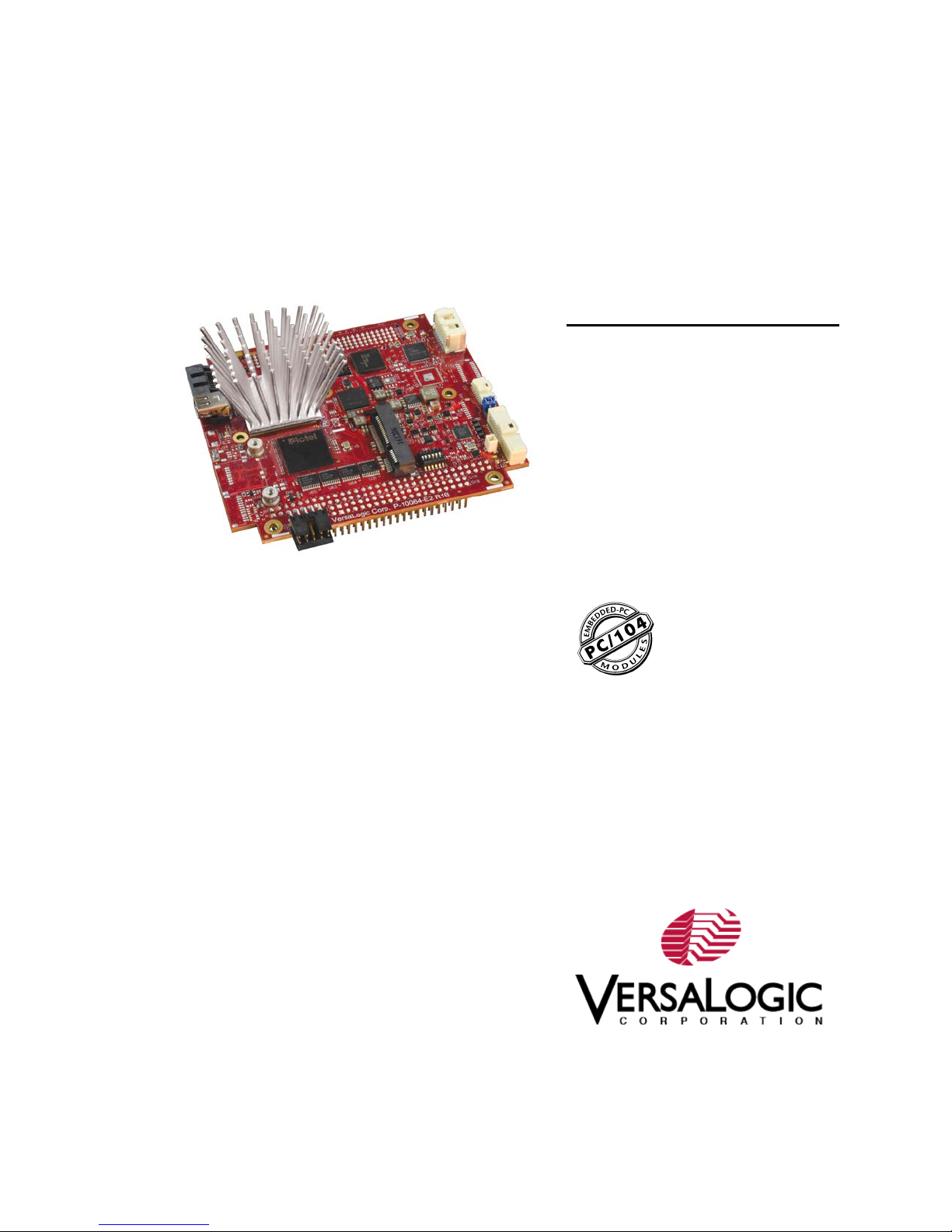
Intel® Atom™-based Single
Board Computer with Ethernet ,
Video, USB, SATA, Serial I/O,
Digital I/O, Counter/Timers, Mini
PCIe, mSATA and
PCI/104-Plus Interface.
Page 2

WWW.VERSALOGIC.COM
12100 SW Tualatin Road
Tualatin, OR 97062-7341
(503) 747-2261
Fax (971) 224-4708
Copyright © 2018 VersaLogic Corp. All right s r es er ved.
Notice:
Although every effort has been made to ensure this document is error-free, VersaLogic makes no
representations or warranties with respect to this product and specifically disclaims any implied warranties
of merchantability or fitness for any particular purpose.
VersaLogic reserves the right to revise this product and associated documentation at any time without
obligation to notify anyone of such changes.
PC/104, PC/104-Plus, and the PC/104 logo are trademarks of the PC/104 Consortium.
EPM-39 Programmer’s Reference Manual ii
Page 3

Product Release Notes
Release 1
First release of this document.
Support
The EPM-39 support page contains additional information and resources for this product
including:
Reference Manual (PDF format)
Operating system information and software drivers
Data sheets and manufacturers’ links for chips used in this product
BIOS information and upgrades
Utility routines and benchmark software
The VersaTech KnowledgeBase is an invaluable resource for resolving technical issues with
your VersaLogic product.
VersaTech KnowledgeBase
EPM-39 Programmer’s Reference Manual iii
Page 4

Contents
Introduction ................................................................................................................... 1
Related Documents ............................................................................................................. 1
System Resources and Maps ....................................................................................... 2
Memory Map ...................................................................................................................... 2
Interrupts ............................................................................................................................. 2
FPGA Registers ............................................................................................................. 4
FPGA I/O Space ................................................................................................................. 4
ISA Bus Addressing and LPC I/O and Memory Map ........................................... 4
FPGA Register Map ........................................................................................................... 5
FPGA Register Descriptions............................................................................................... 8
Product Information Registers ............................................................................... 8
BIOS and Jumper Status Register .......................................................................... 9
Timer Registers .................................................................................................... 10
Miscellaneous FPGA Registers ........................................................................... 13
Programming Information f or Hardware Interfaces .................................................. 28
Processor WAKE# Capabilities........................................................................................ 28
Watchdog Timer ............................................................................................................... 28
Programmable LED .......................................................................................................... 28
Tables
Table 1: Memory Map ........................................................................................................ 2
Table 2: I/O Map ................................................................................................................. 3
Table 3: FPGA I/O Map ...................................................................................................... 4
Table 4: ISA Bus I/O Map .................................................................................................. 4
Table 5: ISA Memory Map ................................................................................................. 4
Table 6: PCR – Product Code and LED Register ............................................................... 8
Table 7: PSR – Product Status Register .............................................................................. 8
Table 8: SCR –Status/Control Register .............................................................................. 9
Table 9: TICR – 8254 Timer Interrupt Control Register .................................................. 10
Table 10: TISR – 8254 Timer Interrupt Status Register ................................................... 11
Table 11: TCR – 8254 Timer Control Register ................................................................ 12
Table 12: MISCR1 – Misc. Control Register #1 .............................................................. 13
Table 13: MISCSR2 – Misc. Control Register #2 ............................................................ 14
Table 14: MISCR3 – Misc. Control Register #3 .............................................................. 15
Table 15: AUXDIR – AUX GPIO Direction Control Register ........................................ 16
Table 16: AUXPOL – AUX GPIO Polarity Control Register .......................................... 16
EPM-39 Programmer’s Reference Manual iv
Page 5

Contents
Table 17: AUXOUT – AUX GPIO Output Control Register ........................................... 16
Table 18: AUXIN – AUX GPIO Input Status Register .................................................... 17
Table 19: AUXICR – AUX GPIO Interrupt Mask Register ............................................. 17
Table 20: AUXISTAT – AUX GPIO Interrupt Status Register ........................................ 17
Table 21: AUXMODE1 – AUX I/O Mode Register ........................................................ 18
Table 22: WDT_CTL – Watchdog Control Register ........................................................ 19
Table 23: WDT_VAL – Watchdog Value Register .......................................................... 20
Table 24: XCVRMODE – COM Transceiver Mode Register .......................................... 20
Table 25: AUXMODE2 - AUX I/O Mode Register #2 .................................................... 21
Table 29: TEMPICR – Temperature Interrupt Control Register ...................................... 22
Table 30: TEMPISTAT – Temperature Interrupt Status Register .................................... 22
Table 31: UART1CR – UART1 Control Register (COM1) ............................................. 23
Table 32: UARTMODE1 – UART MODE Register #1 ................................................... 24
Table 33: UARTMODE2 – UART MODE Register #2 ................................................... 26
Table 34: ISACON1 – ISA Control Register #1 ............................................................... 27
Table 35: ISACON2 – ISA Control Register #2 ............................................................... 27
EPM-39 Programmer’s Reference Manual v
Page 6

1
This document provides information for users requiring register-level information for developing
applications with the VL-EPM-39.
Related Documents
The following documents available are on the EPM-39 Product Support Web Page:
EPM-39 Hardware Reference Manual – provides information on the board’s hardware
features including connectors and all interfaces.
Introduction
EPM-39 Programmer’s Reference Manual 1
Page 7

00000h – 9FFFFh
Legacy system (DOS) area
A0000h – B7FFFh
ISA memory area (VGA frame buffer is not accessible)
B8000h – BFFFFh
Text mode buffer
C0000h – CFFFFh
Video BIOS area
D0000h – DFFFFh
PCI ROM expansion area
E0000h – FFFFFh
Legacy BIOS (reserved)
2
Memory Map
Table 1: Memory Map
Interrupts
The LPC SERIRQ is used for interrupt interface to the BayTrail SoC.
System Resources and Maps
Address Range Description
Each of the following devices can have an IRQ interrupt assigned to it and each with an interrupt
enable control for IRQ3, IRQ4, IRQ5, IRQ6, IRQ7, IRQ9, IRQ10, and IRQ11:
8254 timers (with three interrupt status bits)
8 AUX GPIOs (with one interrupt status bit)
COM 1 UART (with 16550 interrupt status bits)
Watchdog timer (one status bit)
Thermal event interrupts
ISA interrupts
The ISA bus supports 11 interrupts: IRQ3, IRQ4, IRQ5, IRQ6, IRQ7, IRQ9, IRQ10, IRQ11,
IRQ12, IRQ14, and IRQ15. There is an interrupt enable control for each and by default they are
all disabled. ISA bus interrupts simply pass through to the SERIRQ (no capture in the FPGA).
Common interrupts can be assigned to multiple devices if software can deal with it (this is
common on UARTs being handled by a common ISR).
Interrupt status bits for everything except the UARTs will “stick” and are cleared by a “writeone” to a status register bit. The 16550 UART interrupts behave as defined for the 16550
registers and are a pass-through to the LPC SERIRQ.
Per the VersaAPI standard, anytime an interrupt on the SERIRQ is enabled, the slot becomes
active. All interrupts in the SERIRQ are high-true so when the slot becomes active, the slot will
be low when there is no interrupt and high when there is an interrupt.
EPM-39 Programmer’s Reference Manual 2
Page 8

Table 2: I/O Map
3F8h – 3FFh
COM1 serial port default
400h – 47Fh
ACPI / Power management (reserved)
500h – 5FFh
PCH GPIO (reserved)
C80h – CBBh
EPM-39 FPGA Board Control Registers
CBCh – CBFh
EPM-39 FPGA 8254 Timer Registers
I/O Address Range Device/Owner
System Resources and Maps
EPM-39 Programmer’s Reference Manual 3
Page 9

0xC80 – 0xCBB
FPGA registers
60 bytes
0xCBC – 0xCBF
8254 timer address registers
4 bytes
0xC80 - 0xCBF
FPGA registers
64 bytes
All other LPC I/O cycles
ISA bus
Depends on SoC LPC I/O traffic
0x0 – 0xFFFFFF LPC memory cycles
ISA bus
Depends on SoC LPC memory traffic
0x1000000 and higher LPC memory
cycles
TPM is the only memory device on the
LPC bus
3
FPGA I/O Space
The FPGA is mapped into I/O space on the LPC bus
FPGA access: LPC I/O space
FPGA access size: All 8-bit byte accesses (16-bit like registers are aligned on 16-bit word
boundaries to make word access possible in software but the LPC bus still splits the accesses
into two 8-bit accesses)
FPGA address range: 0xC80 to 0xCBF (64-byte window)
The three 8254 timers only require four bytes of addressing and are located at the end of the
64-byte I/O block. The only requirement is that the base address must be aligned on a 4-byte
block. The table below lists the FPGA’s I/O map.
FPGA Register s
Table 3: FPGA I/O Map
Address Range Device Size
ISA BUS ADDRE S S ING AND LPC I/O AND MEMORY MAP
The FPGA implements an LPC-to-ISA bridge. The LPC bus only has the he FPGA uses I/O
space 0xC80-0xCBF. The ISA bus memory address space is16 Mbytes (24-bits of address); ISA
busy I/O addressing is limited to 64 Kbytes (16 bits of address). As such, the following will be
the allowed memory and I/O map for the ISA bus.
All LPC I/O cycles that are unclaimed by the FPGA will pass through to the ISA bus. Similarly,
all LPC memory cycles below 16 Mbytes will be passed through to the ISA bus.
Table 4: ISA Bus I/O Map
Address Range Device Size
Table 5: ISA Memory Map
Address Range Device Size
EPM-39 Programmer’s Reference Manual 4
Ignored by FPGA
Page 10
EPM-39 Programmer’s Reference Manual 5
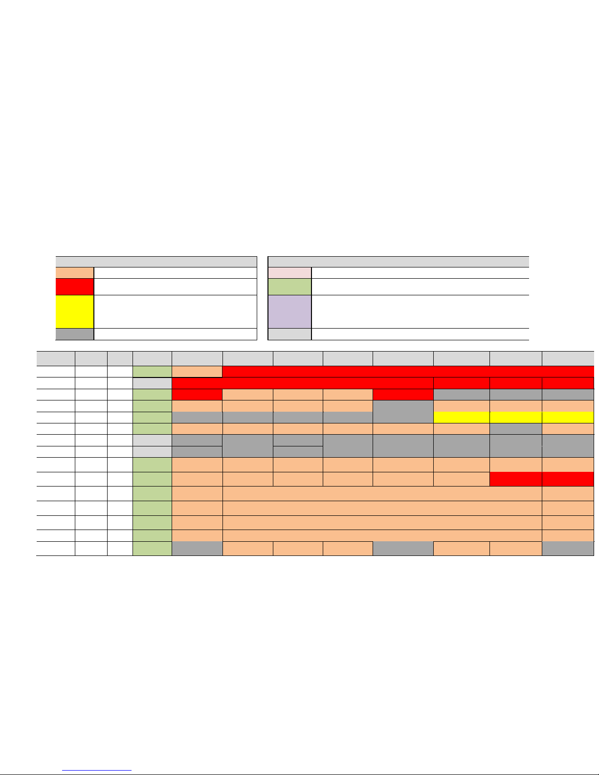
FPGA Register Map
Register Access Key
Reset Status Key
R/W Read/Write POR Power-on reset (only resets one time when input power comes on)
RO Read-only (status or reserved) Platform
Resets prior to the processor entering t he S0 power state (that is, at power-on
and in sleep states)
R/WC Read-status/Write-1-to-Clear resetSX
• If FPGA_PSEN is a '0' in MISCSR1 (default setting), t hen this is the
same as the Platform reset.
• If FPGA_PSEN is a programmed to a '1', then it is the same as the
Power-On Reset (POR).
RSVD Reserved. Only write 0 to this bit; ignore all read values. n/a Reset doesn't apply to status or res erved registers
Identifier
I/O
Address
Offset
Reset
Type
D7 D6 D5 D4 D3 D2 D1 D0
PCR C80 0 Platform PLED PRODUCT_CODE
PSR C81 1 n/a REV_LEVEL EXTEMP CUSTOM BETA
SCR C82 2 Platform LED_DEBUG WORKVER
RSVD
RSVD RSVD
TICR C83 3 Platform IRQEN IRQSEL2 IRQSEL1 IRQSEL0 RSVD IMASK_TC5 IMASK_TC4 IMASK_TC3
TISR C84 4 Platform RSVD RSVD RSVD RSVD RSVD ISTAT_TC5 ISTAT_TC4 ISTAT_TC3
TCR C85 5 Platform TIM5GATE TIM4GATE TIM3GATE TM45MODE TM4CLKSEL TM3CLKSEL RSVD TMRFULL
Reserved C86 6 n/a RSVD RSVD RSVD RSVD RSVD RSVD RSVD RSVD
Reserved C87 7 n/a RSVD RSVD RSVD RSVD RSVD RSVD RSVD RSVD
Reserved
C88 8 n/a RSVD RSVD RSVD RSVD RSVD RSVD RSVD RSVD
Reserved
C89 9 n/a RSVD RSVD RSVD RSVD RSVD RSVD RSVD RSVD
Reserved
C8A A n/a RSVD RSVD RSVD
Reserved
C8B B n/a RSVD RSVD RSVD
Reserved
C8C C n/a RSVD RSVD RSVD
Reserved C8D D n/a RSVD RSVD RSVD
Reserved
C8E E n/a RSVD RSVD RSVD RSVD RSVD RSVD RSVD RSVD
Page 11

FPGA Registers
EPM-39 Programmer’s Reference Manual 6
Identifier
I/O
Address
Offset
Reset
Type
D7 D6 D5 D4 D3 D2 D1 D0
Reserved C8F F n/a
RSVD RSVD RSVD RSVD RSVD RSVD RSVD RSVD
MISCSCR1
C90 10 POR
RSVD RSVD RSVD RSVD RSVD RSVD FPGA_PSEN MINI_PSDIS
MISCSR2 C91 11 POR
USB_HUBMODE
W_DISABLE USB_USBID USB_HUBDIS USB_PBDIS USB_OBDIS
MISCSR3 C92 12 Platform RSVD RSVD RSVD RSVD USB_PBOC PBRESET RSVD RSVD
Reserved C93 13 n/a RSVD RSVD RSVD RSVD RSVD RSVD RSVD RSVD
AUXDIR CA1 21 resetSX
DIR_GPIO8 DIR_GPIO7 DIR_GPIO6 DIR_GPIO5 DIR_GPIO4 DIR_GPIO3 DIR_GPIO2 DIR_GPIO1
AUXPOL CA2 22 resetSX
POL_GPIO8 POL_GPIO7 POL_GPIO6 POL_GPIO5 POL_GPIO4 POL_GPIO3 POL_GPIO2 POL_GPIO1
AUXOUT CA3 23 resetSX
OUT_GPIO8 OUT_GPIO7 OUT_GPIO6 OUT_GPIO5 OUT_GPIO4 OUT_GPIO3 OUT_GPIO2 OUT_GPIO1
AUXIN CA4 24 n/a
IN_GPIO8 IN_GPIO7 IN_GPIO6 IN_GPIO5 IN_GPIO4 IN_GPIO3 IN_GPIO2 IN_GPIO1
AUXIMASK
CA5 25 Platform IMASK_GPIO8 IMASK_GPIO7 IMASK_GPIO6 IMASK_GPIO5 IMASK_GPIO4 IMASK_GPIO3 IMASK_GPIO2 IMASK_GPIO1
AUXISTAT
CA6 26 Platform ISTAT_GPIO8 ISTAT_GPIO7 ISTAT_GPIO6 ISTAT_GPIO5 I STAT_GPIO4 ISTAT_GPIO3 ISTAT_GPIO2 ISTAT_GPIO1
AUXMODE1
CA7 27 resetSX MODE_GPIO8 MODE_GPIO7 MODE_GPIO6 MODE_GPIO5 MODE_GPIO4 MODE_GPIO3 MODE_GPIO2 MODE_GPIO1
WDT_CTL CA8 28 Platform
IRQEN IRQSEL2 IRQSEL1 IRQSEL0
RSVD
RESET_EN WDT_EN WDT_STAT
WDT_VAL CA9 29 Platform MSB
<========================>
LSB
XCVRMODE
CAA 2A Platform RSVD
RSVD
RSVD
RSVD
RSVD
RSVD
COM2_MODE COM1_MODE
AUXMODE2
CAB 2B Platform
IRQEN IRQSEL2 IRQSEL1 IRQSEL0
RSVD RSVD RSVD RSVD
FANCON CAC 2C Platform RSVD RSVD RSVD RSVD RSVD RSVD RSVD
FAN_OFF
Reserved CAD 2D n/a RSVD RSVD RSVD RSVD RSVD RSVD RSVD RSVD
FANTACHLS
CAE 2E Platform MSB
<========================>
LSB
FANTACHMS
CAF 2F Platform MSB
<========================>
LSB
TEMPICR CB0 30 Platform IRQEN IRQSEL2 IRQSEL1 IRQSEL0 MASK_BATTLOW IMASK_EVENT
IMASK_THERM
IMASK_ALERT
TEMPISTAT
CB1 31 Platform BATTLOW RSVD RSVD RSVD ISTAT_BATTLOW ISTAT_EVENT ISTAT_THERM ISTAT_ALERT
UART1CR CB2 32 Platform IRQEN IRQSEL2 IRQSEL1 IRQSEL0 UART1_BASE3 UART1_BASE2 UART1_BASE1 UART1_BASE0
UART2CR CB3 33 Platform IRQEN IRQSEL2 IRQSEL1 IRQSEL0 UART2_BASE3 UART2_BASE2 UART2_BASE1 UART2_BASE0
Reserved CB4 34 n/a RSVD RSVD RSVD RSVD RSVD RSVD RSVD RSVD
Reserved CB5 35 n/a RSVD RSVD RSVD RSVD RSVD RSVD RSVD RSVD
UARTMODE1
CB6 36 Platform RSVD RSVD
UART2_485ADC UART1_485ADC
RSVD RSVD UART2_EN UART1_EN
Page 12

FPGA Registers
EPM-39 Programmer’s Reference Manual 7
Identifier
I/O
Address
Offset
Reset
Type
D7 D6 D5 D4 D3 D2 D1 D0
UARTMODE2
CB7 37 Platform RSVD RSVD RSVD RSVD RSVD RSVD RSVD FAST_MODE
ISACON1 CB8 38 Platform ISA_IRQ11 ISA_IRQ10 ISA_IRQ9 ISA_IRQ7 ISA_IRQ6 ISA_IRQ5 ISA_IRQ4 ISA_IRQ3
ISACON2 CB9 39 Platform RSVD RSVD RSVD RSVD RSVD ISA_IRQ15 ISA_IRQ14 ISA_IRQ12
Reserved CBA 3A n/a RSVD RSVD RSVD RSVD RSVD RSVD RSVD RSVD
Reserved CBB 3B n/a RSVD RSVD RSVD RSVD RSVD RSVD RSVD RSVD
8254_ADD0
CBC 3C Platform MSB
<========================>
LSB
8254_ADD1
CBD 3D Platform MSB
<========================>
LSB
8254_ADD2
CBE 3E Platform MSB
<========================>
LSB
8254_ADD3
CBF 3F Platform MSB
<========================>
LSB
Page 13
1 – LED is on (can be used by sof tware)
6-0
PRODUCT_CODE
0010001
Product Code for the EPM-39 (0x11)
1 – Extended Temp (probably always set)
1 – Custom Product or P LD/ F PGA
FPGA Register Descriptions
Register Access Key
R/W Read/Write
RO Read-only (status or reserved)
R/WC Read-status/Write-1-to-Clear
RSVD Reserved. Only write 0 to this bit; ignore all read values.
PRODUCT INFORMATION REGISTERS
This register drives the PLED on the paddleboard. It also provides read access to the product
code.
Table 6: PCR – Product Code and LED Register
Bit Identifier Access Default Description
7 PLED R/W 0
Drives the programm abl e LED on the paddleboard.
0 – LED is off (default)
RO
Table 7: PSR – Product Status Register
Bit Identifier Access Default Description
Revision level of the PLD (incremented every FPGA release)
7:3 REV_LEVEL[4:0]
2 EXTEMP
1 CUSTOM
0 BETA
RO
RO
RO
RO
N/A
N/A
N/A
N/A
0 – Indicates product i on release revision level when BETA
status bit (bit 0) i s set to ‘0’
1 – Indicates development release revision level when BETA
status bit (bit 0) i s set to ‘1’
Extended or Standard Temp Status (set via external resistor):
0 – Standard Temp
Custom or Standard Product Status (set in FPGA):
0 – Standard Product
Beta or Production Status (set in FPGA):
1 – Beta (or Debug)
0 – Production
EPM-39 Programmer’s Reference Manual 8
Page 14

BIOS AND JUMPER STATUS REGISTER
1 – LED is on (indicates FPGA is programmed by default)
1 – FPGA is in a working stat e (not rel eased)
1
N/A
Reserved. Writes are ignored; reads always return 0.
0
0
Reserved. Writes are ignored; reads always return 0.
Table 8: SCR –Status/Control Register
Bit Identifier Access Default Description
FPGA Registers
7
RESERVED
6
RESERVED
5
RESERVED
LED_DEBUG
4
WORKVER
3
RESERVED
2
RESERVED RO
RESERVED RO
Note: This corresponds to the setting of posit i on 6 of the SW1 Configuration Switch block. Refer to the EPM-39
Hardware Reference Manual for more i nformation regarding the configurat i on switches.
R/W
RO
RO
Debug LED (controls the yellow LED):
0
0 – LED is off and follows it s pri mary function (MSATA_DAS)
Status used to indic at e that the FPGA is not off i cially released
N/A
N/A Reserved. Wri t es are ignored; reads always return 0.
and is still in a working st at e.
0 – FPGA is released
EPM-39 Programmer’s Reference Manual 9
Page 15

FPGA Registers
1 – Interrupts enabled
111 – IRQ11
1 – Interrupt enabled
1 – Interrupt enabled
TIMER REGISTERS
The FPGA implements an 8254-compatible timer/counter that includes three 16-bit timers.
Table 9: TICR – 8254 Timer Interrupt Control Register
Bit Identifier Access Default Description
8254 Timer interrupt enable/dis abl e:
7 IRQEN
6-4 IRQSEL(2:0)
R/W
R/W
0
000
0 – Interrupts disabled
8254 Timer interrupt IRQ select in LPC SERIRQ:
000 – IRQ3
001 – IRQ4
010 – IRQ5
011 – IRQ10
100 – IRQ6
101 – IRQ7
110 – IRQ9
3 RESERVED
2 IMSK_TC5
1 IMSK_TC4
0 IMSK_TC3
RO
R/W
R/W
R/W
0 Reserved. Writes are ignored; reads always return 0.
8254 timer #5 interrupt mask:
0
0 – Interrupt disabled
8254 timer #4 interrupt mask:
0
0 – Interrupt disabled
1 – Interrupt enabled
8254 timer #3 interrupt mask:
0
0 – Interrupt disabled
EPM-39 Programmer’s Reference Manual 10
Page 16

Table 10: TISR – 8254 Timer Interrupt Status Register
7
RESERVED
0
Reserved. Writes are ignored; reads always return 0.
6
RESERVED
0
Reserved. Writes are ignored; reads always return 0.
5
RESERVED
0
Reserved. Writes are ignored; reads always return 0.
4
RESERVED
0
Reserved. Writes are ignored; reads always return 0.
3
RESERVED
0
Reserved. Writes are ignored; reads always return 0.
1 level
Bit Identifier Access Default Description
RO
RO
RO
RO
RO
Status for the 8254 Timer #5 output (terminal count) interrupt
when read. This bit is read-status and a write-1-to-clear.
2 ISTAT_TC5
1 ISTAT_TC4
RW/C
RW/C
N/A
N/A
0 – Timer output (term i nal count) has not transitioned f rom 0 to
a 1 level
1 – Timer output (term i nal count) has transitioned from a 0 to a
1 level
Status for the 8254 Timer #4 output (terminal count) interrupt
when read. This bit is read-status and a write-1-to-clear.
0 – Timer output (term i nal count) has not transitioned f rom 0 to
a 1 level
1 – Timer output (term i nal count) has transitioned from a 0 to a
FPGA Registers
0 ISTAT_TC3
RW/C
N/A
Status for the 8254 Timer #3 output (terminal count) interrupt
when read. This bit is read-status and a write-1-to-clear.
0 – Timer output (term i nal count) has not transitioned f rom 0 to
a 1 level
1 – Timer output (term i nal count) has transitioned from a 0 to a
1 level
EPM-39 Programmer’s Reference Manual 11
Page 17

Table 11: TCR – 8254 Timer Control Register
internal clocking.
internal clocking
Timer #5 is always on internal cl ock if configured as a 16-bit c l ock
1
RESERVED
0
Reserved. Writes are ignored; reads always return 0.
Bit Identifier Access Default Description
Debug/Test Only: Controls the “gate” signal on 8254 timer #5 when not
using an external gate signal:
7 TMR5GATE
6 TMR4GATE
5 TMR3GATE
R/W
R/W
R/W
0 – Gate on signal GCTC5 is disabl ed
0
1 – Gate on signal GCTC5 is enabled
Always set to 0 when configuring tim er modes except when TMRFULL
is ‘0’ and then it should be set to ‘1’ and not changed unless us i ng
Controls the “gate” signal on 8254 timer #4 when not using an external
gate signal:
0 – Gate on signal GCTC4 is disabl ed
0
1 – Gate on signal GCTC4 is enabled
Always set to 0 when configuring timer modes except when TMRFULL
is ‘0’ and then it should be set to ‘1’ and not changed unless us i ng
internal clocking
Controls the “gate” signal on 8254 timer #3 when not using an external
gate signal:
0 – Gate on signal GCTC3 is disabl ed
0
1 – Gate on signal GCTC3 is enabled
Always set to 0 when configuring timer modes except when TMRFULL
is ‘0’ and then it should be set to ‘1’ and not changed unless us i ng
FPGA Registers
4 TM45MODE
3 TM4CLKSEL
2 TM3CLKSEL
0 TMRFULL
R/W
R/W
R/W
RO
R/W
Mode to set timers #4 and #5 i n:
0 – Timer #4 and #5 form one 32-bit timer controlled by timer #1 signals
1 – Timer #4 and Timer #5 are separate 16-bit timers with their own
0
control signals.
Almost always used in 32-bit mode especially when TMRFULL is a ‘0’
(the 16-bit timer #5 if of l i mited use)
Timer #4 Clock Selec t :
0 – Use internal 4.125 MHz clock (deri ved f rom PCI clock)
0
1 – Use external ICTC4
Timer #3 Clock Selec t :
0
0 – Use internal 4.125 MHz clock (deri ved f rom PCI clock)
1 – Use external ICTC3 assigned to Di gi tal I/O
DIOs to use for timer signals (TMREN m ust be a ‘1’ in the DIOCR
register to use the timers).
0 – 4-wire timers and DIO16-DIO13 are external timer control signals
1 – 8-wire and DIO16-DIO9 are external timer control s i gnal s
Because the gates-cont rol s are not connected to digital I /Os when
0
TMRFULL is a ‘0’, the TIMxGATE gate controls in this register are us ed
so they need to be set to ‘1’ and shoul d not be toggled during operation
with external timers (since there i s no continuous clock to synchronize
them to) but can be toggled if using the internal clock. If you need
gating in external modes, set T MRFULL to a ‘ 1’ .
EPM-39 Programmer’s Reference Manual 12
Page 18

FPGA Registers
FPGA_PSEN
power control signal and the inverse of MINI_PSDIS.
MISCELLANEOUS FPGA REGISTERS
MISCR1 – Miscellaneous Contr ol Register #1
This is a register in the always-on power well of the FPGA. It holds its state during sleep modes
and can only be reset by a power cycle. This is a placeholder register for features like pushing
the power-button and also for software initiated resets should those be needed. This register is
only reset by the main power-on reset since it must maintain its state in Sleep modes (for
example, S3).
Table 12: MISCR1 – Misc. Control Register #1
Bits Identifier Access Default Description
7-2 Reserved
1 FPGA_PSEN
RO
R/W
000000 Reserved. Writes are i gnored; reads always return 0.
FPGA digital I/O and AUX GPIO bank I/O power enable
0 – The digital I/O and AUX GPIO bank will be powered down in
sleep modes (only power in S0)
1 – The digital I/O and AUX GPIO bank will not be powered down in
0
sleep modes and the confi guration will remain.
The FPGA 3.3 V I/O bank power switc h i s controlled by the “OR” of
the S0 power control signal and FPGA_PSEN.
Note: Some regist er res ets are conditional on the state of
Minicard 3.3 V power disable
0 – Minicard 3.3 V power stays on always (this is norm al l y how
minicards operate if they support any Wake events)
0 MINI_PSDIS
R/W
0
1 – Minicard 3.3 V power will be turned off when not in S0 (in s l eep
modes).
The Minicard 3.3 V power switch is cont rol l ed by t he “OR” of the S0
MISCR2 – Miscellaneous Contr ol Register #2
This is a register in the always-on power well of the FPGA. It holds its state during sleep
modes and can only be reset by a power cycle. It is primarily used for control signals for
the always-powered Ethernet controllers and the USB hubs. This register is only reset by
the main power-on reset since it must maintain its state in sleep modes (for example, S3).
EPM-39 Programmer’s Reference Manual 13
Page 19

Table 13: MISCSR2 – Misc. Control Register #2
entering all sleep modes). USB ports cannot be used to wake-up
Reserved
1 – Ethernet controller is di s abl ed (O f f)
disable VBUS power)
1 – USB2513 hub is in reset
and then a 0
Bit
Identifier
7
USB_HUBMODE
6 W_DISABLE
5
4 ETHOFF0
Access Default
R/W
R/W
R/W
Description
Determines whether the hub resets onl y onc e (to support wake-up from
sleep modes on USB ports ) or resets every time it enters sleep modes
using the platform res et :
0
0 – USB hub is reset once at power on. Use USB_HUBDIS t o manually
control the reset if nec es sary. This supports USB wake-up modes
1 – USB hub is reset by platform reset every time (will be reset when
Used to control the W_DISABLE (Wireless Disable) signal going to the
PCIe Mincard:
0 – W_DISAB LE signal is not asserted (E nabl ed)
0
1 – W_DISAB LE signal is asserted (Dis abl ed)
Note: There are other control sourc es that can be configured to control
this signal and if enabled the control becomes the “OR” of al l sources
Used to disable the Ethernet controller #0 (controls the E TH_OF F #
input to the I210-IT):
0
0 – Ethernet controller is enabl ed (On)
FPGA Registers
3 USB_USBID
2 USB_HUBDIS
1 USB_PBDIS
0 USB_OBDIS
R/W
R/W
R/W
R/W
Set to use the “ID” signal on t he on-board USB 3.0 signal to control the
VBUS power. USB OTG (on-the-go) uses this si gnal t o tell whether an
“A” or “B” cable is plugged in a mi cro-USB 3.0 “AB” connector. When
USB_USBID is set t o a ‘ 1’ , an “A” cable will turn VBUS power on and a
“B” will turn it off (because “B” devices are not supported).
0
0 – Do not use “ID” signal to cont rol VBUS power (VBUS power
controlled only by USB_OBDIS)
1 – Use “ID” signal to control V BUS power (USB_OBDIS will still
Control the reset on the USB2513B Hub.
0
0 – USB2513 hub is enabled (reset released)
Disable control for the paddleboard USB port VBUS power switches
(there are two power-switches but they have a common power enable
and overcurrent status)
0 – VBUS power switches are enabled
0
1 – VBUS power switched are disabled.
Note: The I2164 power switches latc h-of f i n overcurrent and can only
be re-enabled by a power-cycle or by setting this bit t o a 1, wait >1 ms,
Disable control for the on-board USB port VBUS power switches (there
are two with a common overcurrent):
0 – VBUS power switches are enabled
0
1 – VBUS power switched are disabled.
Note: The I2164 power switches latc h-of f i n overcurrent and can only
be re-enabled by a power-cycle of by setting this bit to a 1 and then a 0
with at least 1 ms in bet ween
EPM-39 Programmer’s Reference Manual 14
Page 20

MISCR3 – Miscellaneous Contr ol Register #3
1 – Overcurrent is asserted (power switch i s off)
1-0
Reserved
00
Reserved. Writes are ignored; reads always return 0.
This register sets the SMBus addresses on the 4-Port PCIe Switch.
Table 14: MISCR3 – Misc. Control Register #3
Bits Identifier Access Default Description
7-4 Reserved
3 USB_PBOC
2 PBRESET
RO
RO
R/W
RO
0000 Reserved. Writes are ignored; reads always return 0.
Reads the overcurrent status f or the USB paddleboard power
switches (there are two power switches for the four port s but they
N/A
---
have a common overcurrent st atus).
0 – Overcurrent is not assert ed (power switch i s on)
When written to, t hi s will do the same thing as pushi ng the reset
button, which could be useful f or a software-initiated watchdog.
0 – No action
1 – Activate the reset push-button
Note: Because this generat es a reset that will reset this register, it
isn’t likely a value of a ‘1’ can ever be read-back, so it is s omewhat
“write-only”.
FPGA Registers
EPM-39 Programmer’s Reference Manual 15
Page 21

FPGA Registers
1 – Output
edge used.
1 – Asserts the output (1 i f polarity not-inverted, 0 if inverted)
AUXDIR – AUX GPIO Direction Control Register
This register controls the direction of the eight AUX GPIO signals.
This reset depends on the state of the FPGA_PSEN signal. If FPGA_PSEN is a ‘0’ then the reset
is the power-on and Platform Reset. If FPGA_PSEN is a ‘1’ then this register is only reset at
power-on.
Table 15: AUXDIR – AUX GPIO Direction Control Register
Bit Identifier Access Default Description
Sets the direction of the AUX GPIOx lines. For each bit:
7-0 DIR_GPIO[8:1]
R/W
0
0 – Input
AUXPOL – AUX GPIO Polarity Control Register
This register controls the polarity of the eight AUX GPIO signals.
This reset depends on the state of the FPGA_PSEN signal. If FPGA_PSEN is a ‘0’ then the reset
is the power-on and Platform Reset. If FPGA_PSEN is a ‘1’ then this register is only reset at
power-on.
Table 16: AUXPOL – AUX GPIO Polarity Control Register
Bits Identifier Access Default Description
Sets the polarity of the A UX GPIOx lines . F or each bit:
0 – No inversion
7-0 POL_GPIO[8:1]
R/W
0
1 – Invert
Note: This impac ts the polarity as well as the interrupt status
AUXOUT – AUX GPIO Output Control Register
This register sets the AUX GPIO output value. This value will only set the actual output if the
GPIO direction is set as an output. Reading this register does not return the actual input value of
the GPIO (use the AUXIN register for that). As such, this register can actually be used to detect
input/output conflicts.
This reset depends on the state of the FPGA_PSEN signal. If FPGA_PSEN is a ‘0’ then the reset
is the power-on and Platform Reset. If FPGA_PSEN is a ‘1’ then this register is only reset at
power-on.
Table 17: AUXOUT – AUX GPIO Output Control Register
Bits Identifier Access Default Description
Sets the AUX GPIOx output values. For eac h bi t :
7-0 OUT_GPIO[8:1]
R/W
0 – De-asserts the output (0 if polarity not-inverted, 1 if i nvert ed)
0
EPM-39 Programmer’s Reference Manual 16
Page 22
FPGA Registers
de-asserted if pol ari ty inverted
1 – Interrupt enabled
Bits
Identifier
Access
Default
Description
(POL_DIOx=0) or high-to-low (POL_DIOx=1).
AUXIN – AUX GPIO I/O Input Status Register
This registers sets the AUX GPIO input value. It will read the input value regardless of the
setting on the direction (that is, it always reads the input). This reads the actual state of the GPIO
pin into the part.
Table 18: AUXIN – AUX GPIO Input Status Register
Bits Identifier Access Default Description
Reads the GPIOx input status. For each bit:
7-0 IN_GPIOIO[8:1]
RO
N/A
0 – Input de-asserted if polari t y not -inverted;
asserted if polarity inverted
1 Input asserted if polarit y not-inverted;
AUXIMASK – AUX GPIO Interrupt Mask Register
This is the interrupt mask registers for the AUX GPIOs and the interrupt enable selection. The
reset type is Platform Reset because interrupts always have to be setup after exiting sleep states.
Table 19: AUXICR – AUX GPIO Interrupt Mask Register
Bits Identifier Access Default Description
GPIOx interrupt mask. For each bit:
7-0
IMASK_GPIO[8:1]
R/W
0
0 – Interrupt disabled
AUXISTAT – AUX GPIO I/O Interrupt Status Register
Table 20: AUXISTAT – AUX GPIO Interrupt Status Register
GPIOx interrupt status. A read ret urns the interrupt status. Writing
7-0
ISTAT_GPIO[8:1]
RW/C
N/A
a ‘1’ clears the interrupt s tatus.
This bit is set t o a ‘ 1’ on a t ransition from low-to-high
EPM-39 Programmer’s Reference Manual 17
Page 23

FPGA Registers
be read.
be read.
be read.
polarity control applies. T he GPIO input status can still be read.
be read.
1 – Reserved for future secondary mode (do not set)
1 – Reserved for future secondary mode (do not set)
1 – Reserved (same as GPIO)
AUXMODE1– AUX I/O Mode Register #1
These two registers selected the mode on each AUX GPIO. This reset depends on the state of the
FPGA_PSEN signal. If FPGA_PSEN is a ‘0’ then the reset is the power-on and Platform Reset.
If FPGA_PSEN is a ‘1’ then this register is only reset at power-on.
Table 21: AUXMODE1 – AUX I/O Mode Register
Bit Identifier Access Default Description
GPIO8 mode.
0 – GPIO (I/O)
7 MODE_GPIO8
6 MODE_GPIO7
R/W
R/W
1 – W_DISAB LE (input). In this mode, the GPIO is passed
0
through to the W_DISABLE# signal.
The GPIO polarity control applies. The GPIO input status can still
GPIO7 mode.
0 – GPIO (I/O)
1 – SLEEP (output). In t hi s mode, the GPIO indic ates that the
0
CPU is in a sleep mode (S3 or higher).
The GPIO polarity control applies. The GPIO input status can still
5 MODE_GPIO6
4 MODE_GPIO5
3 MODE_GPIO4
2 MODE_GPIO3
1 MODE_GPIO2
0 MODE_GPIO1
R/W
R/W
R/W
R/W
R/W
R/W
GPIO6 mode.
0 – GPIO (I/O)
1 – PWM0 from B ayTrai l SoC (output). In this mode, the GPIO
0
tracks the PWM0 signal from the BayTrail SoC.
The GPIO polarity control applies. The GPIO input status can still
GPIO5 mode.
0 – GPIO (I/O)
0
1 – Power Good (output). In this m ode, the GPIO indicates that
the board is in the S0 state and all power is good. The GPIO
GPIO4 mode.
0 – GPIO (I/O)
1 – Watchdog Res et (output). In this mode, the GPIO will be the
0
watchdog timer trigger output that signals external equipment that
the watchdog fired.
The GPIO polarity control applies. The GPIO input status can still
GPIO3 mode.
0
0 – GPIO (I/O)
GPIO2 mode.
0
0 – GPIO (I/O)
GPIO1 mode.
0
0 – GPIO (I/O)
EPM-39 Programmer’s Reference Manual 18
Page 24

WDT_CTL – Watchdog Control Register
1 – Interrupts enabled
111 – IRQ11
1 – Board will be reset if the Watchdog “fires”
Note:
a reset occurs
Reset type is Platform.
Table 22: WDT_CTL – Watchdog Control Register
Bits Identifier Access Default Description
Watchdog int errupt enable/disable:
7 IRQEN
6-4 IRQSEL(2:0)
R/W
R/W
0
000
0 – Interrupts disabled
Watchdog interrupt I RQ select in LPC SERIRQ:
000 – IRQ3
001 – IRQ4
010 – IRQ5
011 – IRQ10
100 – IRQ6
101 – IRQ7
110 – IRQ9
FPGA Registers
3 Reserved
2 RESET_EN
1 WDT_EN
0 WDT_STAT
RO
R/W
R/W
RO
0 Reserved. Writes are ignored; reads always return 0.
Enable the Watchdog to assert the push-button reset if it “fires”.
0
0 – Watchdog will not reset the board
Watchdog Enable:
0 – Watchdog is disabled
0
1 – Watchdog is enabled
The WDT_VAL regis ter must be set before enabling.
Watchdog St at us:
0 – Watchdog disabled or watchdog has not “fired”
1 – Watchdog fired.
Note: Once set to a ‘1’, it will remain so until any of the following
0
occurs:
• the WDT_VAL register is written to
• the WDT_EN is di sabled
•
EPM-39 Programmer’s Reference Manual 19
Page 25

FPGA Registers
set to a ‘1’.
7-4
Reserved
0000
Reserved. Writes are igno red; reads always return 0.
1 – RS422/485
1 – RS422/485
WDT_VAL – Watchdog Value Register
This register sets the number of seconds for a Watchdog prior to enabling the watchdog. By
writing this value, the watchdog can be prevented from “firing”. A watchdog fires whenever this
registers value is all 0s, so it must be set to a non-zero value before enabling the watchdog to
prevent an immediate “firing”. Reset type is Platform.
The value written should always be 1 greater than the desired timeout value due to a 0-1 second
“tick” error band (values written should range from 2-255 because a 1 could cause an immediate
trigger); that is, the actual timeout is WDT_VAL seconds with a -1 second to 0 second error
band.
Table 23: WDT_VAL – Watchdog Value Register
Bits Identifier Access Default Description
7-0 WDT_VAL(7:0)
R/W
0x00
Number of seconds before the Watchdog fires . By default, it is
set to zero which results in an immediate watchdog if WDT_EN is
XCVRMODE – COM Transceiver Mode Register
Sets the RS232 vs RS422/485 mode on the COM port Transceivers. These drive the UART_SEL
signals from the FPGA to the Transceivers.
Reset type is Platform.
Note: The values shown are for the default BIOS configuration.
Table 24: XCVRMODE – COM Transceiver Mode Register
Bits Identifier Access Default Description
RO
3-2 Reserved
1 COM2_MODE
0 COM1_MODE
RO
R/W
R/W
00 Reserved. Writes are ignored; reads al ways return 0.
COM2 Transceiver mode:
0
0 – RS232
COM1 Transceiver mode:
0
0 – RS232
EPM-39 Programmer’s Reference Manual 20
Page 26

FPGA Registers
1 – Interrupts enabled
111 – IRQ11
AUXMODE2– AUX I/O Mode Register #2
This register defines the interrupt mapping for the AUX GPIOs. Reset type is Platform.
Table 25: AUXMODE2 - AUX I/O Mode Register #2
Bits Identifier Access Default Description
AUX GPIO interrupt enable/disable:
7 IRQEN
6-4 IRQSEL(2:0)
R/W
R/W
0
000
0 – Interrupts disabled
AUX GPIO interrupt IRQ select in LPC SERIRQ:
000 – IRQ3
001 – IRQ4
010 – IRQ5
011 – IRQ10
100 – IRQ6
101 – IRQ7
110 – IRQ9
3-0 Reserved
RO
0000 Reserved. Writes are ignored; reads always return 0.
EPM-39 Programmer’s Reference Manual 21
Page 27

FPGA Registers
1 – Interrupts enabled
111 – IRQ11
1 – Interrupt enabled.
1 – Interrupt enabled.
1 – Interrupt enabled.
Reserved
Reserved
status. Writing a ‘1’ will clear the interrupt status
interrupt status. Writing a ‘1’ clears the interrupt status
TEMPICR – Temperature Interrupt Contr ol Regi st er
This is the interrupt mask register for the temperature sensor thermal alerts and the DDR3
SODIMM EVENT signals and the interrupt enable and selection. The SODIMM may not have
any temperature event capability. Reset type is Platform.
Table 26: TEMPICR – Temperature Interrupt Control Register
Bits Identifier Access Default Description
7 IRQEN
6-4 IRQSEL(2:0)
R/W
R/W
000
Temperature interrupt enable/di sable:
0
0 – Interrupts disabled
Temperature interrupt IRQ s el ect in LPC SERIRQ:
000 – IRQ3
001 – IRQ4
010 – IRQ5
011 – IRQ10
100 – IRQ6
101 – IRQ7
110 – IRQ9
3 IMASK_BATTLOW
2 IMASK_EVENT
1 IMASK_THERM
0 IMASK_ALERT
R/W
R/W
R/W
R/W
Battery-low interrupt mask:
0
0 – Interrupt disabled
SODIMM EVENT output interrupt mask:
0
0 – Interrupt disabled
Temperature Sensor THERM output i nterrupt mask:
0
0 – Interrupt disabled
1 – Interrupt enabled.
Temperature Sensor ALERT output interrupt mask:
0
0 – Interrupt disabled
TEMPISTAT – Temperature Interrupt Status Register
Reset type: n/a.
Table 27: TEMPISTAT – Temperature Interrupt Status Register
Bits Identifier Access Default Description
7
6-4 Reserved
3
2 ISTAT_EVENT
RO
RO
RW/C
RW/C
000 Reserved. Writ es are ignored; reads always return 0.
N/A
SODIMM EVENT interrupt st atus. A read returns the interrupt
1 ISTAT_THERM
0 ISTAT_ALERT
EPM-39 Programmer’s Reference Manual 22
RW/C
RW/C
N/A
N/A
Temperature Sensor THERM interrupt status. A read returns the
interrupt status. Writing a ‘1’ clears the interrupt status
Temperature Sensor ALERT i nterrupt status. A read returns t he
Page 28

UART1CR – UART1 Control Regi st er (COM1)
Note: The BIOS (via ACPI) may modify this register when in an ACPI-capable
unless you are using a non-ACPI operating system.
111 – IRQ11
1010-1111 [ These values are reserved; do no t use.]
Reset type is Platform.
operating system. The register can be read for status purposes but do not write to it
Table 28: UART1CR – UART1 Control Register (COM1)
Bits Identifier Access Default Description
UART interrupt enable/disabl e:
7 IRQEN
6-4 IRQSEL(2:0)
R/W
R/W
0
001
0 – Interrupts disabled
1 – Interrupts enabled
UART interrupt IRQ selec t in LPC SERIRQ:
000 – IRQ3
001 – IRQ4 [ COM1 Default]
010 – IRQ5
011 – IRQ10
100 – IRQ6
101 – IRQ7
110 – IRQ9
FPGA Registers
3-0 UART1_BASE(3:0)
R/W
0000
UART Base Address:
0000 - 3F8h [ COM1 Default]
0001 - 2F8h
0010 - 3E8h
0011 - 2E8h
0100 - 200h
0101 - 208h
0110 - 220h
0111 - 228h
1000 - 238h
1001 - 338h
EPM-39 Programmer’s Reference Manual 23
Page 29

FPGA Registers
Note: Terminal software, expecting an RS-232 port, may set RTS to '1' and disable the
transmitting when in Manual Direction Control mode.
7-6
Reserved
00
Reserved. Writes are i gnored; reads always return 0.
XCVRMODE register must also be set to a ’1’
3-2
Reserved
00
Reserved. Writes are ignored; reads always return 0.
1 – Tx and RTS outputs are enabled
1 – Tx and RTS outputs are enabled
When a UART is disabled, there will be no decoding of the UART I/O address range
and any I/O activity will be passed to the ISA bus (this allows COM ports to be on the
UARTMODE1 – UART MODE REGISTER #1
When the COM Transceiver Mode is set to RS422/485 (in the XCVRMODE register) and the
RS-485 Automatic Direction Control is enabled (e.g., UART1_485ADC set to ‘1’) then the
transceiver Tx output is enabled when there are bytes to transmit and the transceiver Tx output is
disabled (i.e., tri-stated) when there are no bytes to transmit.
When the COM Transceiver Mode is set to RS422/485 and Automatic Direction Control is
disabled (e.g., UART1_485ADC set to ‘0’) then the UART is in Manual Direction Control mode
and the transceiver Tx output enable is controlled by software using the RTS bit in the UART
Modem Control Register.
RTS = '0' - Transceiver Tx output is enabled.
RTS = '1' - Transceiver Tx output is disabled (i.e., tri-stated).
Reset type is Platform.
transmitter when initializing an RS-422/485 port in Manual Direction Control mode.
Application software that handles the RS-422/485 port should set RTS to '0' to enable
Table 29: UARTMODE1 – UART MODE Register #1
Bits Identifier Access Default Description
RO
COM2 RS-485 Automatic Direc tion Control:
0 – Disabled
5 UART2_485ADC
4 UART1_485ADC
1 UART2_EN
0 UART1_EN
R/W
R/W
RO
R/W
R/W
0
1 – Enabled
Note: Only enable in RS-485 mode. The COM2_MODE in
XCVRMODE register must also be set to a ’1’
COM1 RS-485 Automat i c Direction Control:
0 – Disabled
0
1 – Enabled
Note: Only enable in RS-485 mode. . T he COM1_MODE in
UART #2 Output Enable:
0 – Tx and RTS outputs are disabled and UART I/ O accesses
1
are passed to the ISA bus.
UART #1 Output Enable:
0 – Tx and RTS outputs are disabled and UART I/ O accesses
1
are passed to the ISA bus
Note:
EPM-39 Programmer’s Reference Manual 24
Page 30

Note:
ISA bus if the FPGA UARTs are not used). This means that the UART must be
enabled before accessing registers.
FPGA Registers
EPM-39 Programmer’s Reference Manual 25
Page 31

FPGA Registers
7-1
Reserved
0000000
Reserved. Writes are ignored; reads always return 0.
Note: This must be set to ‘1’ to use baud rates above 115,200.
UARTMODE2 – UART MODE REGISTER #2
Standard software (the BIOS and the operating system) assumes the baud-rate clock is
1.8432 MHz and programs the divisors accordingly; however, a faster oscillator is needed for
baud rates higher than 115,200.
The FAST_MODE bit in this register is used to shift the divisor by 4 bits (multiply by 16) so that
the legacy baud rate comes out correctly for the 16x UART clock. This bit must be set to use
rates above 115,200 and may require custom software.
Reset type is Platform.
Note: The values shown are for the default BIOS configuration.
Table 30: UARTMODE2 – UART MODE Register #2
Bits Identifier Access Default Description
RO
Sets how the baud-rate divisor for the 16550 UART s are
interpreted (applies to all ports ):
0 FAST_MODE
R/W
0
0 – Divisor is multi pl i ed by 16 (legacy mode for 1.8432 MHz
clock)
1 – Divisor is not modified (fast mode for 16x 1.8432 MHz clock)
EPM-39 Programmer’s Reference Manual 26
Page 32

FPGA Registers
1 – Pass ISA interrupt to SERIRQ
1 – Pass ISA interrupt to SERIRQ
1 – Pass ISA interrupt to SERIRQ
1 – Pass ISA interrupt to SERIRQ
1 – Pass ISA interrupt to SERIRQ
1 – Pass ISA interrupt to SERIRQ
7
RSVD
0
Reserved. Only write 0 to this bit; ignore all read values.
6-3
Reserved
0
Reserved. Writes are ignored; reads always return 0.
1 – Pass ISA interrupt to SERIRQ
ISACONx (x = 1,2) – ISA Control Registers
These register are used to enable ISA interrupts on the LPC SERIRQ. ISA interrupts simply pass
through to SERIRQ and - per the ISA bus standard - are always high-true. The SERIRQEN
control bit is not used for the ISA interrupt mask and should not be set until the interrupt
processing is ready.
Note: The values shown are for the default BIOS configuration.
Table 31: ISACON1 – ISA Control Register #1
Bits Identifier Access Default Description
7 ISA_IRQ11
R/W
0
Interrupt enable for ISA int errupt
0 – Do not pass ISA interrupt to SERIRQ
6 ISA_IRQ10
5 ISA_IRQ9
4 ISA_IRQ7
3 ISA_IRQ6
2 ISA_IRQ5
1 ISA_IRQ4
0 ISA_IRQ3
R/W
R/W
R/W
R/W
R/W
R/W
R/W
0
0
0
0
0
0
0
Interrupt enable for ISA int errupt
0 – Do not pass ISA interrupt to SERIRQ
Interrupt enable for ISA int errupt
0 – Do not pass ISA interrupt to SERIRQ
1 – Pass ISA interrupt to SERIRQ
Interrupt enable for ISA int errupt
0 – Do not pass ISA interrupt to SERIRQ
Interrupt enable for ISA int errupt
0 – Do not pass ISA interrupt to SERIRQ
Interrupt enable for ISA int errupt
0 – Do not pass ISA interrupt to SERIRQ
Interrupt enable for ISA int errupt
0 – Do not pass ISA interrupt to SERIRQ
Interrupt enable for ISA int errupt
0 – Do not pass ISA interrupt to SERIRQ
1 – Pass ISA interrupt to SERIRQ
Table 32: ISACON2 – ISA Control Register #2
Bits Identifier Access Default Description
RSVD
RO
2 ISA_IRQ15
1 ISA_IRQ14
R/W
R/W
0
0
Interrupt enable for ISA int errupt
0 – Do not pass ISA interrupt to SERIRQ
1 – Pass ISA interrupt to SERIRQ
Interrupt enable for ISA int errupt
0 – Do not pass ISA interrupt to SERIRQ
0 ISA_IRQ12
EPM-39 Programmer’s Reference Manual 27
R/W
0
Interrupt enable for ISA int errupt
0 – Do not pass ISA interrupt to SERIRQ
1 – Pass ISA interrupt to SERIRQ
Page 33

4
Programming Info rmat ion for Hardware
Processor WAKE# Capabilities
The following devices can wake up the processor using the PCIE_WAKE# signal to the SoC:
Ethernet port 0 controller
FPGA via the AUX connector GPIO(3) secondary function
The following USB devices can wake up the processor using the in-band SUSPEND protocol:
Any of the three Paddleboard USB Ports via the USB2513B Hub
The USB 2.0 port on the paddleboard that directly connects to the Baytrail SoC
Watchdog Timer
Interfaces
A Watchdog timer is implemented within the FPGA. When triggered, the Watchdog timer can set a
status bit, generate an interrupt and/or hit the push-button-reset. The Watchdog timer implements a
1-255 second timeout.
The Watchdog time out is set in an 8-bit register (WDT_VAL). When the Watchdog is enabled, the
WDT_VAL will start to count down. If the Watchdog is enabled and whenever WDT_VAL is zero,
the Watchdog is triggered (so a non-zero value must be written before enabling the watchdog).
Software must periodically write a non-zero value to WDT_VAL to prevent this trigger. The value
written should always be 1 greater than the desired timeout value due to a 0-1 second error band.
Values written should be from 2-255 because a 1 could cause an immediate trigger); that is, the
actual timeout is WDT_VAL seconds with a -1 second to 0 second error band.
The Watchdog control/status register(s) have bits for the following:
Watchdog enable/disable (disabled by default)
Watchdog timeout status (This is cleared when the Watchdog is disabled or when a new value is
written to WDT_VAL. Writing WDT_VAL would be the interrupt-acknowledge.)
Watchdog interrupt IRQ select (from the same list of eight interrupts supported on the LPC
SERIRQ)
Interrupt enable
Board reset enable (when set, the board will be reset when the Watchdog timer expires).
Programmable LED
User I/O connector J4 includes an output signal for attaching a software controlled LED. Connect
the cathode of the LED to J4, pin 16; connect the anode to +3.3 V. An on-board resistor limits the
current when the circuit is turned on. A programmable LED is provided on the CBR-4005B
paddleboard. Refer to the EPM-39 Hardware Reference Manual for the location of the
Programmable LED on the CBR-4005B paddleboard.
EPM-39 Programmer’s Reference Manual 28
*** End of document ***
 Loading...