

Page 1
Programmer’s
Reference
Manual
REV. May 2018
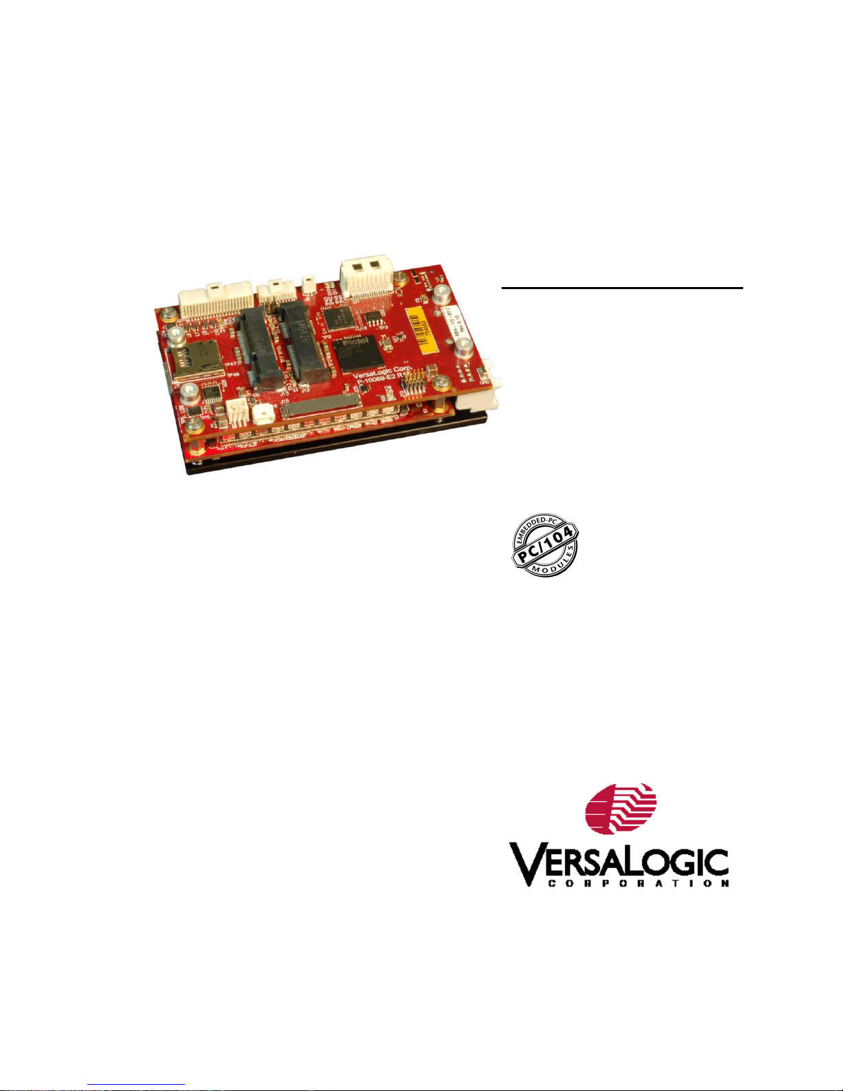
Osprey
(VL-EPU-3311)
Intel® Atom™ E38xx-based
Embedded Processing Unit with
SATA, Ethernet, USB, Serial,
Video, Mini PCIe Sockets, and
microSD.
Page 2

WWW.VERSALOGIC.COM
12100 SW Tualatin Road
Tualatin, OR 97062-7341
(503) 747-2261
Fax (971) 224-4708
Copyright © 2016-2018 VersaLogic Corp. All rights reserved.
Notice:
Although every effort has been made to ensure this document is error-free, VersaLogic makes no
representations or warranties with respect to this product and specifically disclaims any implied warranties
of merchantability or fitness for any particular purpose.
VersaLogic reserves the right to revise this product and associated documentation at any time without
obligation to notify anyone of such changes.
PC/104, PC/104-Plus, and the PC/104 logo are trademarks of the PC/104 Consortium.
EPU-3311 Programmer’s Reference Manual ii
Page 3

Product Release Notes
VersaTech KnowledgeBase
Release 1.3
Updated the Uartmode1 – Uart Mode Register #1 section
Release 1.2
Updated the UART Base Addresses in Tables 23 and 24.
Release 1.1
Updated Related Documents section.
Release 1
First release of this document.
Support
The EPU-3311 support page, at www.versalogic.com/private/ospreysupport.asp contains additional
information and resources for this product including:
Reference Manual (PDF format)
Operating system information and software drivers
Data sheets and manufacturers’ links for chips used in this product
BIOS information and upgrades
Utility routines and benchmark software
The VersaTech KnowledgeBase is an invaluable resource for resolving technical issues with
your VersaLogic product.
EPU-3311 Programmer’s Reference Manual iii
Page 4

Contents
Introduction ................................................................................................................... 1
Related Documents ............................................................................................................. 1
System Resources ........................................................................................................ 2
Interrupts ............................................................................................................................. 2
FPGA I/O Space ................................................................................................................. 2
FPGA Registers ............................................................................................................. 3
Register Access Key ........................................................................................................... 3
Reset Status Key ................................................................................................................. 3
FPGA Register Map ........................................................................................................... 4
FPGA Register Descriptions............................................................................................... 7
Product Information Registers ............................................................................... 7
BIOS and Jumper Status Register .......................................................................... 8
Timer Registers ...................................................................................................... 8
Miscellaneous FPGA Registers ........................................................................... 11
Programming Information for Hardware Interfaces .................................................. 24
Watchdog Timer ............................................................................................................... 24
Programmable LED .......................................................................................................... 24
Processor WAKE# Capabilities........................................................................................ 25
Tables
Table 1: FPGA I/O Map ...................................................................................................... 2
Table 2: FPGA Register Map.............................................................................................. 4
Table 3: PCR – Product Code and LED Register ............................................................... 7
Table 4: PSR – Product Status Register .............................................................................. 7
Table 5: SCR –Status/Control Register .............................................................................. 8
Table 6: TICR – 8254 Timer Interrupt Control Register .................................................... 8
Table 7: TISR – 8254 Timer Interrupt Status Register ....................................................... 9
Table 8: TCR – 8254 Timer Control Register .................................................................. 10
Table 9: MISCSR1 – Misc. Control Register #1 .............................................................. 11
Table 10: MISCSR2 – Misc. Control Register #2 ............................................................ 12
Table 11: MISCSR3 – Misc. Control Register #3 ............................................................ 13
Table 12: AUXDIR – AUX GPIO Direction Control Register ........................................ 14
Table 13: AUXPOL – AUX GPIO Polarity Control Register .......................................... 14
Table 14: AUXOUT – AUX GPIO Output Control Register ........................................... 14
Table 15: AUXIN – AUX GPIO Input Status Register .................................................... 15
Table 16: AUXICR – AUX GPIO Interrupt Mask Register ............................................. 15
EPU-3311 Programmer’s Reference Manual iv
Page 5

Contents
Table 17: AUXISTAT – AUX GPIO Interrupt Status Register ........................................ 15
Table 18: AUXMODE1 – AUX I/O Mode Register ........................................................ 16
Table 19: WDT_CTL – Watchdog Control Register ........................................................ 17
Table 20: WDT_VAL – Watchdog Control Register ....................................................... 18
Table 21: XCVRMODE – COM Transceiver Mode Register .......................................... 18
Table 22: AUXMODE2 - AUX I/O Mode Register #2 .................................................... 19
Table 23: UART1CR – UART1 Control Register (COM1) ............................................. 20
Table 24: UART2CR – UART2 Control Register (COM2) ............................................. 21
Table 25: UARTMODE1 – UART MODE Register #1 ................................................... 22
Table 26: UARTMODE2 – UART MODE Register #2 ................................................... 23
EPU-3311 Programmer’s Reference Manual v
Page 6

1
This document provides information for users requiring register-level information for developing
applications with the VL-EPU-3311.
Related Documents
The following documents available are on the EPU-3311 Product Support Web Page:
VL-EPU-3311 Hardware Reference Manual – provides information on the board’s hardware
features including connectors and all interfaces.
This document is available through the software page:
VersaAPI Installation and Reference Guide – describes the shared library of API calls for
reading and controlling on-board devices on certain VersaLogic products.
Introduction
EPU-3311 Programmer’s Reference Manual 1
Page 7

Address Range
Device
Size
0x1C80 – 0x1CBB
FPGA registers
60 bytes
0x1CBC – 0x1CBF
8254 timer address registers
4 bytes
2
Interrupts
The LPC SERIRQ is used for interrupt interface to the BayTrail SoC.
Each of the following devices can have an IRQ interrupt assigned to it and each with an interrupt
enable control for IRQ3, IRQ4, IRQ5, IRQ6, IRQ7, IRQ9, IRQ10, and IRQ11:
8254 timers (with three interrupt status bits)
8x GPIOs (with one interrupt status bit per GPIO)
COM 1 UART (with 16550 interrupt status bits)
COM 2 UART (with 16550 interrupt status bits)
Watchdog timer (one status bit)
Common interrupts can be assigned to multiple devices if software can deal with it (this is
common on UARTs being handled by a common ISR).
System Resources
Interrupt status bits for everything except the UARTs will “stick” and are cleared by a “writeone” to a status register bit. The 16550 UART interrupts behave as defined for the 16550
registers and are a pass-through to the LPC SERIRQ.
Per the VersaAPI standard, anytime an interrupt on the SERIRQ is enabled, the slot becomes
active. All interrupts in the SERIRQ are high-true so when the slot becomes active, the slot will
be low when there is no interrupt and high when there is an interrupt.
FPGA I/O Space
The FPGA is mapped into I/O space on the LPC bus. The address range is mapped into a 64 byte
I/O window.
FPGA access: LPC I/O space
FPGA access size: All 8-bit byte accesses (16-bit like registers are aligned on 16-bit word
boundaries to make word access possible in software but the LPC bus still splits the accesses
into two 8-bit accesses)
FPGA address range: 0x1C80 to 0x1CBF (a 64-byte window)
The three 8254 timers only require four bytes of addressing and are located at the end of the
64-byte I/O block. The only requirement is that the base address must be aligned on a 4-byte
block. Table 1 lists the FPGA’s I/O map.
EPU-3311 Programmer’s Reference Manual 2
Table 1: FPGA I/O Map
Page 8
Register Access Key
R/W
Read/Write
RO
Read-only (status or reserved)
R/WC
Read-status/Write-1-to-Clear
RSVD
Reserved. Only write 0 to this bit; ignore all read values.
Reset Status Key
POR
Power-on reset (only resets one time when input power comes on)
Platform
Resets prior to the processor entering the S0 power state (that is, at power-on and in sleep states)
resetSX
If AUX_PSEN is a '0' in MISCSR1 (default setting), then this is the same as the Platform reset.
If AUX_PSEN is a programmed to a '1', then it is the same as the Power-On Reset (POR).
n/a
Reset doesn't apply to status or reserved registers
3
This chapter describes the FPGA registers.
Table 2 (beginning on the following page) lists all 64 FPGA registers
Table 3 (refer to page 7) through Table 26 provide bit-level information on the individual
FPGA registers
Register Access Key
FPGA Registers
Reset Status Key
EPU-3311 Programmer’s Reference Manual 3
Page 9
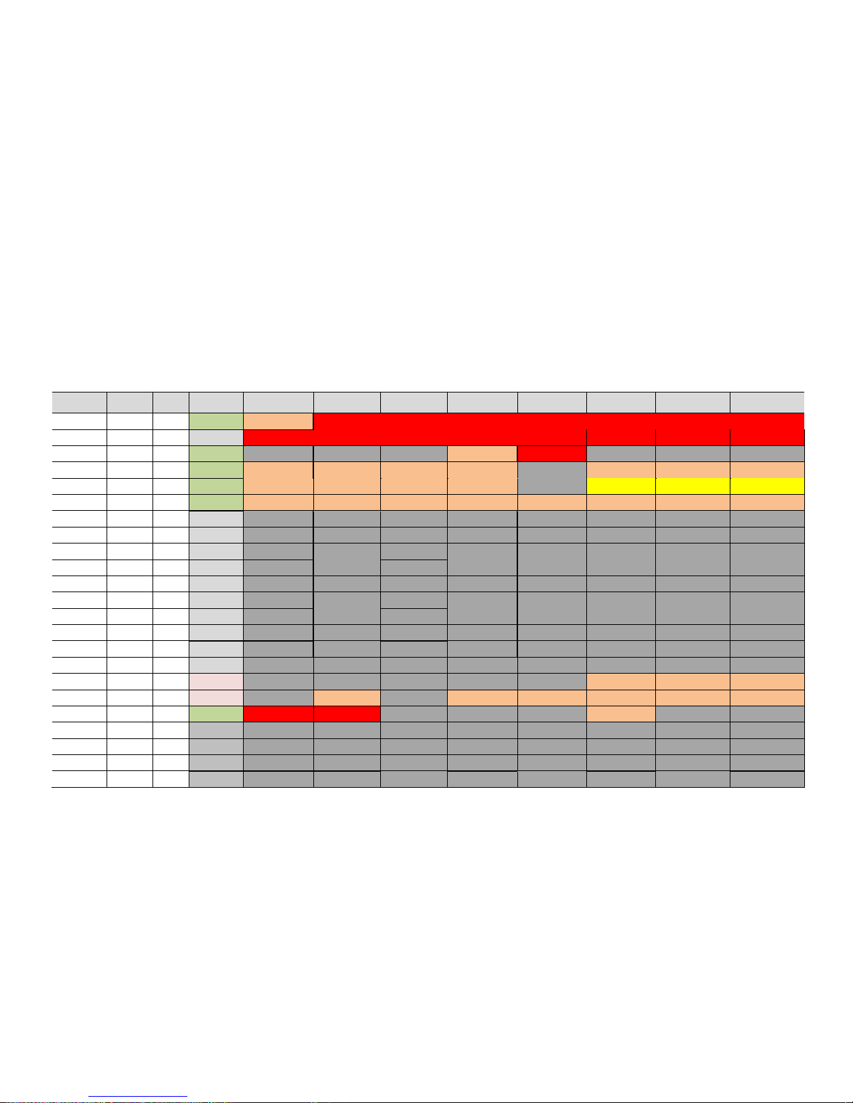
EPU-3311 Programmer’s Reference Manual 4
FPGA Register Map
Table 2: FPGA Register Map
Identifier
I/O
Address
Offset
Reset
Type
D7
D6
D5
D4
D3
D2
D1
D0
PCR
1C80 0 Platform
PLED
PRODUCT_CODE
PSR
1C81 1 n/a
REV_LEVEL
EXTEMP
CUSTOM
BETA
SCR
1C82 2 Platform 0 0
0
LED_DEBUG
WORKVER 0 0 0 TICR
1C83 3 Platform
IRQEN
IRQSEL2
IRQSEL1
IRQSEL0
0
IMASK_TC5
IMASK_TC4
IMASK_TC3
TISR
1C84 4 Platform
INTRTEST
TMRTEST
TMRIN4
TMRIN3
0
ISTAT_TC5
ISTAT_TC4
ISTAT_TC3
TCR
1C85 5 Platform
TIM5GATE
TIM4GATE
TIM3GATE
TM45MODE
TM4CLKSEL
TM3CLKSEL
TMROCTST
TMRFULL
Reserved
1C86 6 n/a 0 0 0 0 0 0 0 0
Reserved
1C87 7 n/a 0 0 0 0 0 0 0 0
Reserved
1C88 8 n/a 0 0 0 0 0 0 0 0
Reserved
1C89 9 n/a 0 0 0 0 0 0 0 0
Reserved
1C8A A n/a 0 0 0 0 0 0 0 0
Reserved
1C1B B n/a 0 0 0 0 0 0 0 0
Reserved
1C8C C n/a 0 0 0 0 0 0 0 0
Reserved
1C8D D n/a 0 0 0 0 0 0 0 0
Reserved
1C8E E n/a 0 0 0 0 0 0 0 0
Reserved
1C8F F n/a 0 0 0 0 0 0 0 0
MISCSR1
1C90
10
POR 0 0 0 0
0
MINI2_PSDIS
AUX_PSEN
MINI1_PSDIS
MISCSR 2
1C91
11
POR
0
W_DISABLE
0
ETH0_OFF
USB_USBID
USB_PB2DIS
USB_PB1DIS
USB_OBDIS
MISCSR 3
1C92
12
Platform
PROCHOT
LVDS_OC 0 0 0 PBRESET 0 0
Reserved
1C93
13
n/a 0 0 0 0 0 0 0 0
Reserved
1C94
14
n/a 0 0 0 0 0 0 0 0
Reserved
1C95
15
n/a 0 0 0 0 0 0 0 0
Reserved
1C96
16
n/a 0 0 0 0 0 0 0 0
Page 10

FPGA Registers
EPU-3311 Programmer’s Reference Manual 5
Identifier
I/O
Address
Offset
Reset
Type
D7
D6
D5
D4
D3
D2
D1
D0
Reserved
1C97
17
n/a 0 0 0 0 0 0 0 0
Reserved
1C98
18
n/a 0 0 0 0 0 0 0 0
Reserved
1C99
19
n/a 0 0 0 0 0 0 0 0
Reserved
1C9A
1A
n/a 0 0 0 0 0 0 0 0
Reserved
1C9B
1B
n/a 0 0 0 0 0 0 0 0
Reserved
1C9C
1C
n/a 0 0 0 0 0 0 0 0
Reserved
1C9D
1D
n/a 0 0 0 0 0 0 0 0
Reserved
1C9E
1E
n/a 0 0 0 0 0 0 0 0
Reserved
1C9F
1F
n/a 0 0 0 0 0 0 0 0
Reserved
1CA0
20
n/a 0 0 0 0 0 0 0 0
AUXDIR
1CA1
21
resetSX
DIR_GPIO8
DIR_GPIO7
DIR_GPIO6
DIR_GPIO5
DIR_GPIO4
DIR_GPIO3
DIR_GPIO2
DIR_GPIO1
AUXPOL
1CA2
22
resetSX
POL_GPIO8
POL_GPIO7
POL_GPIO6
POL_GPIO5
POL_GPIO4
POL_GPIO3
POL_GPIO2
POL_GPIO1
AUXOUT
1CA3
23
resetSX
OUT_GPIO8
OUT_GPIO7
OUT_GPIO6
OUT_GPIO5
OUT_GPIO4
OUT_GPIO3
OUT_GPIO2
OUT_GPIO1
AUXIN
1CA4
24
n/a
IN_GPIO8
IN_GPIO7
IN_GPIO6
IN_GPIO5
IN_GPIO4
IN_GPIO3
IN_GPIO2
IN_GPIO1
AUXIMASK
1CA5
25
Platform
IMASK_GPIO8
IM ASK_ GPI O7
IM ASK_ GPI O6
IMASK_GPIO5
IM AS K_G PIO 4
IM AS K_G PIO 3
IM ASK _ GP IO2
IM ASK _ GP IO1
AUXISTAT
1CA6
26
Platform
ISTAT_GPIO8
ISTAT_GPIO7
ISTAT_GPIO6
ISTAT_GPIO5
ISTAT_GPIO4
ISTAT_GPIO3
IS T AT_ GPI O 2
IS T AT_ GPI O 1
AUXMODE1
1CA7
27
resetSX
MO DE_G PIO 8
MO DE _G PIO7
MO DE _G PIO6
MO DE_G PIO 5
MO DE_G PIO 4
MO DE_G PIO 3
MOD E_ GPI O2
MOD E_ GPI O1
WDT_CTL
1CA8
28
Platform
IRQEN
IRQSEL2
IRQSEL1
IRQSEL0
0
RESET_EN
WDT_EN
WDT_STAT
WDT_VAL
1CA9
29
Platform
MSB
<========================>
LSB
XCVRMODE
1CAA
2A
Platform 0 0 0 0 0 0
COM2_MODE
COM1_MODE
AUXMODE2
1CAB
2B
Platform
IRQEN
IRQSEL2
IRQSEL1
IRQSEL0 0 0 0 0
Reserved
1CAC
2C
n/a 0 0 0 0 0 0 0 0
Reserved
1CAD
2D
n/a 0 0 0 0 0 0 0 0
Reserved
1CAE
2E
n/a 0 0 0 0 0 0 0 0
Reserved
1CAF
2F
n/a 0 0 0 0 0 0 0 0
Reserved
1CB0
30
n/a 0 0 0 0 0 0 0 0
Reserved
1CB1
31
n/a 0 0 0 0 0 0 0 0
Page 11

FPGA Registers
EPU-3311 Programmer’s Reference Manual 6
Identifier
I/O
Address
Offset
Reset
Type
D7
D6
D5
D4
D3
D2
D1
D0
UART1CR
1CB2
32
Platform
IRQEN
IRQSEL2
IRQSEL1
IRQSEL0
UART1_BASE3
UART1_BASE2
UA RT1 _B ASE 1
UA RT1 _B ASE 0
UART2CR
1CB3
33
Platform
IRQEN
IRQSEL2
IRQSEL1
IRQSEL0
UART2_BASE3
UART2_BASE2
UA RT2 _B ASE 1
UA RT2 _B ASE 0
Reserved
1CB4
34
n/a 0 0 0 0 0 0 0 0
Reserved
1CB5
35
n/a 0 0 0 0 0 0 0 0
UARTM ODE 1
1CB6
36
Platform 0 0
UART2_485ADC
UAR T1_ 485 AD C
0 0 UART2_EN
UART1_EN
UARTM ODE 2
1CB7
37
Platform 0 0 0 0 0 0
0
FAST_MODE
Reserved
1CB8
38
n/a 0 0 0 0 0 0 0 0
Reserved
1CB9
39
n/a 0 0 0 0 0 0 0 0
Reserved
1CBA
3A
n/a 0 0 0 0 0 0 0 0
Reserved
1CBB
3B
n/a 0 0 0 0 0 0 0 0
8254_ADD0
1CBC
3C
Platform
MSB
<========================>
LSB
8254_ADD1
1CBD
3D
Platform
MSB
<========================>
LSB
8254_ADD2
1CBE
3E
Platform
MSB
<========================>
LSB
8254_ADD3
1CBF
3F
Platform
MSB
<========================>
LSB
Page 12

Register Access Key
R/W
Read/Write
RO
Read-only (status or reserved)
R/WC
Read-status/Write-1-to-Clear
RSVD
Reserved. Only write 0 to this bit; ignore all read values.
Bit
Identifier
Access
Default
Description
7
PLED
R/W
0
Drives the programmable LED on the paddleboard.
0 – LED is off (default)
1 – LED is on
6-0
PRODUCT_CODE
RO
0010011
Product Code for the EPU-3311 (0x13)
Bit
Identifier
Access
Default
Description
7:3
REV_LEVEL[4:0]
RO
N/A
Revision level of the PLD (incremented every FPGA release)
0 – Indicates production release revision level when BETA
status bit (bit 0) is set to ‘0’
1 – Indicates development release revision level when BETA
status bit (bit 0) is set to ‘1’
2
EXTEMP
RO
N/A
Extended or Standard Temp Status (set via external resistor):
0 – Standard Temp
1 – Extended Temp (always set)
1
CUSTOM
RO
N/A
Custom or Standard Product Status (set in FPGA):
0 – Standard Product
1 – Custom Product or PLD/FPGA
0
BETA
RO
N/A
Beta or Production Status (set in FPGA):
1 – Beta (or Debug)
0 – Production
FPGA Register Descriptions
PRODUCT INFORMATION REGISTERS
This register drives the PLED on the paddleboard. It also provides read access to the product
code.
Table 3: PCR – Product Code and LED Register
Table 4: PSR – Product Status Register
EPU-3311 Programmer’s Reference Manual 7
Page 13

BIOS AND JUMPER STATUS REGISTER
Bit
Identifier
Access
Default
Description
7:5
RESERVED
RO
N/A
Reserved. Writes are ignored; reads always return 0.
4
LED_DEBUG
R/W
0
Debug LED (controls the yellow LED):
0 – LED is off and follows its primary function (MSATA_DAS)
1 – LED is on
3
WORKVER
RO
N/A
Status used to indicate that the FPGA is not officially released
and is still in a working state.
0 – FPGA is released
1 – FPGA is in a working state (not released)
2:0
RESERVED
RO
N/A
Reserved. Writes are ignored; reads always return 0.
Bit
Identifier
Access
Default
Description
7
IRQEN
R/W
0
8254 Timer interrupt enable/disable:
0 – Interrupts disabled
1 – Interrupts enabled
6-4
IRQSEL(2:0)
R/W
000
8254 Timer interrupt IRQ select in LPC SERIRQ:
000 – IRQ3
001 – IRQ4
010 – IRQ5
011 – IRQ10
100 – IRQ6
101 – IRQ7
110 – IRQ9
111 – IRQ11
3
RESERVED
RO
0
Reserved. Writes are ignored; reads always return 0.
2
IMASK_TC5
R/W
0
8254 timer #5 interrupt mask:
0 – Interrupt disabled
1 – Interrupt enabled
1
IMASK_TC4
R/W
0
8254 timer #4 interrupt mask:
0 – Interrupt disabled
1 – Interrupt enabled
0
IMASK_TC3
R/W
0
8254 timer #3 interrupt mask:
0 – Interrupt disabled
1 – Interrupt enabled
Table 5: SCR –Status/Control Register
FPGA Registers
TIMER REGISTERS
The FPGA implements an 8254-compatible timer/counter that includes three 16-bit timers.
Table 6: TICR – 8254 Timer Interrupt Control Register
EPU-3311 Programmer’s Reference Manual 8
Page 14

Table 7: TISR – 8254 Timer Interrupt Status Register
Bit
Identifier
Access
Default
Description
7
RESERVED
RO
0
Reserved. Writes are ignored; reads always return 0.
6
RESERVED
RO
0
Reserved. Writes are ignored; reads always return 0.
5
RESERVED
RO
0
Reserved. Writes are ignored; reads always return 0.
4
RESERVED
RO
0
Reserved. Writes are ignored; reads always return 0.
3
RESERVED
RO
0
Reserved. Writes are ignored; reads always return 0.
2
ISTAT_TC5
RW/C
N/A
Status for the 8254 Timer #5 output (terminal count) interrupt
when read. This bit is read-status and a write-1-to-clear.
0 – Timer output (terminal count) has not transitioned from 0 to
a 1 level
1 – Timer output (terminal count) has transitioned from a 0 to a
1 level
1
ISTAT_TC4
RW/C
N/A
Status for the 8254 Timer #4 output (terminal count) interrupt
when read. This bit is read-status and a write-1-to-clear.
0 – Timer output (terminal count) has not transitioned from 0 to
a 1 level
1 – Timer output (terminal count) has transitioned from a 0 to a
1 level
0
ISTAT_TC3
RW/C
N/A
Status for the 8254 Timer #3 output (terminal count) interrupt
when read. This bit is read-status and a write-1-to-clear.
0 – Timer output (terminal count) has not transitioned from 0 to
a 1 level
1 – Timer output (terminal count) has transitioned from a 0 to a
1 level
FPGA Registers
EPU-3311 Programmer’s Reference Manual 9
Page 15

Table 8: TCR – 8254 Timer Control Register
Bit
Identifier
Access
Default
Description
7
TMR5GATE
R/W
0
Debug/Test Only: Controls the “gate” signal on 8254 timer #5 when not
using an external gate signal:
0 – Gate on signal GCTC5 is disabled
1 – Gate on signal GCTC5 is enabled
Always set to 0 when configuring timer modes except when TMRFULL
is ‘0’ and then it should be set to ‘1’ and not changed unless using
internal clocking.
6
TMR4GATE
R/W
0
Controls the “gate” signal on 8254 timer #4 when not using an external
gate signal:
0 – Gate on signal GCTC4 is disabled
1 – Gate on signal GCTC4 is enabled
Always set to 0 when configuring timer modes except when TMRFULL
is ‘0’ and then it should be set to ‘1’ and not changed unless using
internal clocking
5
TMR3GATE
R/W
0
Controls the “gate” signal on 8254 timer #3 when not using an external
gate signal:
0 – Gate on signal GCTC3 is disabled
1 – Gate on signal GCTC3 is enabled
Always set to 0 when configuring timer modes except when TMRFULL
is ‘0’ and then it should be set to ‘1’ and not changed unless using
internal clocking
4
TM45MODE
R/W
0
Mode to set timers #4 and #5 in:
0 – Timer #4 and #5 form one 32-bit timer controlled by timer #1 signals
1 – Timer #4 and Timer #5 are separate 16-bit timers with their own
control signals.
Almost always used in 32-bit mode especially when TMRFULL is a ‘0’
(the 16-bit timer #5 if of limited use)
3
TM4CLKSEL
R/W
0
Timer #4 Clock Select:
0 – Use internal 4.125 MHz clock (derived from LPC clock)
1 – Use external ICTC4 assigned to digital I/O
Timer #5 is always on internal clock if configured as a 16-bit clock
2
TM3CLKSEL
R/W
0
Timer #3 Clock Select:
0 – Use internal 4.125 MHz clock (derived from LPC clock)
1 – Use external ICTC3 assigned to digital I/O
1
TMROCTST
R/W
0
Debug/Test Only: Used to derive OCTCx outputs with TIMxGATE
signals for continuity testing only:
0 – Normal operation
1 – Drive OCTCx outputs with corresponding TMRxGATE control
registers (for example, OCTC4 with TMR4GATE) for continuity testing.
0
TMRFULL
R/W
0
This bit can be read or written to, but it has no function.
FPGA Registers
EPU-3311 Programmer’s Reference Manual 10
Page 16

FPGA Registers
Bits
Identifier
Access
Default
Description
7-3
Reserved
RO
00000
Reserved. Writes are ignored; reads always return 0.
2
MINI2_PSDIS
R/W
0
Minicard #2 3.3 V power disable
0 – Minicard 3.3 V power stays on always (this is normally how
minicards operate if they support any Wake events)
1 – Minicard 3.3 V power will be turned off when not in S0 (in sleep
modes).
The Minicard 3.3 V power switch is controlled by the “OR” of the S0
power control signal and the inverse of MINI2_PSDIS.
1
AUX_PSEN
R/W
0
CBR-4005B 8xGPIO (sometimes called “AUX” GPIOs) I/O Power
Enable
0 – The GPIO pullups will be powered down in sleep modes (only
power in S0)
1 – The GPIO pullups will not be powered down in sleep modes
and the configuration will remain.
This power is used for both the GPIO pullup voltage and for the
3.3V power on Pin 37 of the User Interface connector J2.
Note: Some register resets are conditional on the state of
AUX_PSEN
0
MINI1_PSDIS
R/W
0
Minicard #1 3.3 V power disable
0 – Minicard 3.3 V power stays on always (this is normally how
minicards operate if they support any Wake events)
1 – Minicard 3.3 V power will be turned off when not in S0 (in sleep
modes).
The Minicard 3.3 V power switch is controlled by the “OR” of the S0
power control signal and the inverse of MINI1_PSDIS.
MISCELLANEOUS FPGA REGISTERS
MISCSR1 – Miscellaneous Control Register #1
This is a register in the always-on power well of the FPGA. It holds its state during sleep modes
and can only be reset by a power cycle. This is a placeholder register for features like pushing the
power-button and also for software initiated resets should those be needed.
Reset: This register is only reset by the main power-on reset since it must maintain its state in
Sleep modes (for example, S3).
Table 9: MISCSR1 – Misc. Control Register #1
EPU-3311 Programmer’s Reference Manual 11
Page 17

FPGA Registers
Bit Identifier
Access
Default
Description
7
Reserved
RO
0
Reserved. Writes are ignored; reads always return 0.
6
W_DISABLE
R/W
0
Controls the W_DISABLE (Wireless Disable) signal going to the PCIe
Minicards (disables both minicards if asserted):
0 – W_DISABLE signal is not asserted (Enabled)
1 – W_DISABLE signal is asserted (Disabled)
Note: There are other control sources that can be configured to control
this signal and if enabled the control becomes the “OR” of all sources
5
Reserved
RO
0
Reserved. Writes are ignored; reads always return 0.
4
ETHOFF0
R/W
0
Disables Ethernet controller #0 (controls the ETH_OFF# input to the
I210-IT):
0 – Ethernet controller is enabled (On)
1 – Ethernet controller is disabled (Off)
3
USB_USBID
R/W
0
Set to use the “ID” signal on the on-board USB 3.0 signal to control the
VBUS power. USB OTG (on-the-go) uses this signal to tell whether an
“A” or “B” cable is plugged in a micro-USB 3.0 “AB” connector. When
USB_USBID is set to a ‘1’, an “A” cable will turn VBUS power on and a
“B” will turn it off (because “B” devices are not supported).
0 – Do not use “ID” signal to control VBUS power (VBUS power
controlled only by USB_OBDIS)
1 – Use “ID” signal to control VBUS power (USB_OBDIS will still
disable VBUS power)
2
USB_PB1DIS
R/W
0
Disable control for the paddleboard USB ports 2 and 4 VBUS power
switches (there are two power-switches but they have a common power
enable and overcurrent status)
0 – VBUS power switches are enabled
1 – VBUS power switched are disabled
Note: The power switches latch-off in overcurrent and can only be reenabled by a power-cycle or by setting this bit to a 1, wait >1 ms, and
then a 0
1
USB_PB1DIS
R/W
0
Disable control for the paddleboard USB ports 0 and 1 VBUS power
switches (there are two power-switches but they have a common power
enable and overcurrent status)
0 – VBUS power switches are enabled
1 – VBUS power switched are disabled
Note: The power switches latch-off in overcurrent and can only be reenabled by a power-cycle or by setting this bit to a 1, wait >1 ms, and
then a 0
0
USB_OBDIS
R/W
0
Disable control for the on-board USB 3.0 port VBUS power switch:
0 – VBUS power switch is enabled
1 – VBUS power switch is disabled
Note: The power switch latches-off in overcurrent and can only be reenabled by a power-cycle or by setting this bit to a 1 and then a 0 with
at least 1 ms in between
MISCSR2 – Miscellaneous Control Register #2
This is a register in the always-on power well of the FPGA. It holds its state during sleep
modes and can only be reset by a power cycle. It is primarily used for control signals for
the always-powered Ethernet controllers and the USB hubs. This register is only reset by
the main power-on reset since it must maintain its state in sleep modes (for example, S3).
Table 10: MISCSR2 – Misc. Control Register #2
EPU-3311 Programmer’s Reference Manual 12
Page 18

MISCSR3 – Miscellaneous Control Register #3
Bits
Identifier
Access
Default
Description
7
PROCHOT
RO
N/A
The status of the THERMTRIP signal from the CPU module.
0 – THERMTRIP is not asserted (not hot)
1 – THERMTRIP is asserted
6
LVDS_OC
RO
N/A
The overcurrent status from the LVDS panel power switch. If this is
ever asserted, the LVDS panel enable signal must be de-asserted
and then asserted to “unlatch” the power fault condition on the
power switch.
0 – LVDS Overcurrent is not asserted
1 – LVDS Overcurrent is asserted
3-5
Reserved
RO
N/A
Reads the overcurrent status for the USB paddleboard power
switches (there are two power switches for the four ports but they
have a common overcurrent status).
0 – Overcurrent is not asserted (power switch is on)
1 – Overcurrent is asserted (power switch is off)
2
PBRESET
R/W
---
When written to, this will do the same thing as pushing the reset
button, which could be useful for a software-initiated watchdog.
0 – No action
1 – Activate the reset push-button
Note: Because this generates a reset that will reset this register, it
isn’t likely a value of a ‘1’ can ever be read-back, so it is somewhat
“write-only”.
1-0
Reserved
RO
00
Reserved. Writes are ignored; reads always return 0.
This register enables software to “push” the reset button.
Table 11: MISCSR3 – Misc. Control Register #3
FPGA Registers
EPU-3311 Programmer’s Reference Manual 13
Page 19

FPGA Registers
Bit
Identifier
Access
Default
Description
7-0
DIR_GPIO[8:1]
R/W
0
Sets the direction of the AUX GPIOx lines. For each bit:
0 – Input
1 – Output
Bits
Identifier
Access
Default
Description
7-0
POL_GPIO[8:1]
R/W
0
Sets the polarity of the AUX GPIOx lines. For each bit:
0 – No inversion
1 – Invert
Note: This impacts the polarity as well as the interrupt status
edge used.
Bits
Identifier
Access
Default
Description
7-0
OUT_GPIO[8:1]
R/W
0
Sets the AUX GPIOx output values. For each bit:
0 – De-asserts the output (0 if polarity not-inverted, 1 if inverted)
1 – Asserts the output (1 if polarity not-inverted, 0 if inverted)
AUXDIR – AUX GPIO Direction Control Register
This register controls the direction of the eight AUX GPIO signals.
This reset depends on the state of the FPGA_PSEN signal. If FPGA_PSEN is a ‘0’ then the reset
is the power-on and Platform Reset. If FPGA_PSEN is a ‘1’ then this register is only reset at
power-on.
Table 12: AUXDIR – AUX GPIO Direction Control Register
AUXPOL – AUX GPIO Polarity Control Register
This register controls the polarity of the eight AUX GPIO signals.
This reset depends on the state of the FPGA_PSEN signal. If FPGA_PSEN is a ‘0’ then the reset
is the power-on and Platform Reset. If FPGA_PSEN is a ‘1’ then this register is only reset at
power-on.
Table 13: AUXPOL – AUX GPIO Polarity Control Register
AUXOUT – AUX GPIO Output Control Register
This register sets the AUX GPIO output value. This value will only set the actual output if the
GPIO direction is set as an output. Reading this register does not return the actual input value of
the GPIO (use the AUXIN register for that). As such, this register can actually be used to detect
input/output conflicts.
This reset depends on the state of the FPGA_PSEN signal.
If FPGA_PSEN is a ‘0’ then the reset is the power-on and Platform Reset.
If FPGA_PSEN is a ‘1’ then this register is only reset at power-on.
Table 14: AUXOUT – AUX GPIO Output Control Register
EPU-3311 Programmer’s Reference Manual 14
Page 20

FPGA Registers
Bits
Identifier
Access
Default
Description
7-0
IN_GPIOIO[8:1]
RO
N/A
Reads the GPIOx input status. For each bit:
0 – Input de-asserted if polarity not-inverted;
asserted if polarity inverted
1 Input asserted if polarity not-inverted;
de-asserted if polarity inverted
Bits
Identifier
Access
Default
Description
7-0
IMASK_GPIO[8:1]
R/W
0
GPIOx interrupt mask. For each bit:
0 – Interrupt disabled
1 – Interrupt enabled
Bits
Identifier
Access
Default
Description
7-0
ISTAT_GPIO[8:1]
RW/C
N/A
GPIOx interrupt status. A read returns the interrupt status. Writing
a ‘1’ clears the interrupt status.
This bit is set to a ‘1’ on a transition from low-to-high
(POL_DIOx=0) or high-to-low (POL_DIOx=1).
AUXIN – AUX GPIO I/O Input Status Register
This registers sets the AUX GPIO input value. It will read the input value regardless of the
setting on the direction (that is, it always reads the input). This reads the actual state of the GPIO
pin into the part.
Table 15: AUXIN – AUX GPIO Input Status Register
AUXIMASK – AUX GPIO Interrupt Mask Register
This is the interrupt mask registers for the AUX GPIOs and the interrupt enable selection. The
reset type is Platform Reset because interrupts always have to be setup after exiting sleep states.
Table 16: AUXICR – AUX GPIO Interrupt Mask Register
AUXISTAT – AUX GPIO I/O Interrupt Status Register
Table 17: AUXISTAT – AUX GPIO Interrupt Status Register
EPU-3311 Programmer’s Reference Manual 15
Page 21

FPGA Registers
Bit
Identifier
Access
Default
Description
7
MODE_GPIO8
R/W
0
GPIO8 mode.
0 – GPIO (I/O)
1 – ICTC3 (input)
6
MODE_GPIO7
R/W
0
GPIO7 mode.
0 – GPIO (I/O)
1 – ICTC4 (input)
5
MODE_GPIO6
R/W
0
GPIO6 mode.
0 – GPIO (I/O)
1 – OCTC3 (output)
4
MODE_GPIO5
R/W
0
GPIO5 mode.
0 – GPIO (I/O)
1 – OCTC4 (output)
3
MODE_GPIO4
R/W
0
GPIO4 mode.
0 – GPIO (I/O)
1 – WDOG_RESET# (output only). In this mode, the GPIO will be
the FPGA watchdog timer trigger output that signals external
equipment that the watchdog fired.
The GPIO input status can still be read. Default is low-true.
Setting GPIO polarity to ‘1’ makes it high-true.
2
MODE_GPIO3
R/W
0
GPIO3 mode.
0 – GPIO (I/O)
1 – WAKE# (input only). In this mode, the GPIO is passed
through to the PCI_WAKE# signal.
Default is low-true. Setting GPIO polarity to ‘1’ makes it high-true.
The GPIO input status can still be read.
1
MODE_GPIO2
R/W
0
GPIO2 mode.
0 – GPIO (I/O)
1 – W_DISABLE# (input only). In this mode, the GPIO is passed
through to the W_DISABLE# signal.
The GPIO input status can still be read. Default is low-true.
Setting GPIO polarity to ‘1’ makes it high-true.
0
MODE_GPIO1
R/W
0
GPIO1 mode.
0 – GPIO (I/O)
1 – SLEEP# (input only). This is the sleep signal on the
baseboard power connector. It passes through the SLEEP# input
on the CPU module. Default is low-true. Setting GPIO polarity to
‘1’ makes it high-true.
AUXMODE1– AUX I/O Mode Register #1
These two registers select the mode on each AUX GPIO. This reset depends on the state of the
FPGA_PSEN signal. If FPGA_PSEN is a ‘0’ then the reset is the power-on and Platform Reset:
If AUX_PSEN is a ‘0’ then the reset is the power-on and Platform Reset.
If AUX_PSEN is a ‘1’ then this register is only reset at power-on.
Table 18: AUXMODE1 – AUX I/O Mode Register
EPU-3311 Programmer’s Reference Manual 16
Page 22

WDT_CTL – Watchdog Control Register
Bits
Identifier
Access
Default
Description
7
IRQEN
R/W
0
Watchdog interrupt enable/disable:
0 – Interrupts disabled
1 – Interrupts enabled
6-4
IRQSEL(2:0)
R/W
000
Watchdog interrupt IRQ select in LPC SERIRQ:
000 – IRQ3
001 – IRQ4
010 – IRQ5
011 – IRQ10
100 – IRQ6
101 – IRQ7
110 – IRQ9
111 – IRQ11
3
Reserved
RO
0
Reserved. Writes are ignored; reads always return 0.
2
RESET_EN
R/W
0
Enable the Watchdog to assert the push-button reset if it “fires”.
0 – Watchdog will not reset the board
1 – Board will be reset if the Watchdog “fires”
1
WDT_EN
R/W
0
Watchdog Enable:
0 – Watchdog is disabled
1 – Watchdog is enabled
Note: The WDT_VAL register must be set before enabling.
0
WDT_STAT
RO
0
Watchdog Status:
0 – Watchdog disabled or watchdog has not “fired”
1 – Watchdog fired.
Note: Once set to a ‘1’, it will remain so until any of the following
occurs:
the WDT_VAL register is written to
the WDT_EN is disabled
a reset occurs
Reset type is Platform.
Table 19: WDT_CTL – Watchdog Control Register
FPGA Registers
EPU-3311 Programmer’s Reference Manual 17
Page 23

FPGA Registers
Bits
Identifier
Access
Default
Description
7-0
WDT_VAL(7:0)
R/W
0x00
Number of seconds before the Watchdog fires. By default, it is
set to zero which results in an immediate watchdog if WDT_EN is
set to a ‘1’.
Bits
Identifier
Access
Default
Description
7-4
Reserved
RO
0000
Reserved. Writes are ignored; reads always return 0.
3-2
Reserved
RO
00
Reserved. Writes are ignored; reads always return 0.
1
COM2_MODE
R/W
0
COM2 Transceiver mode:
0 – RS232
1 – RS422/485
0
COM1_MODE
R/W
0
COM1 Transceiver mode:
0 – RS232
1 – RS422/485
WDT_VAL – Watchdog Value Register
This register sets the number of seconds for a Watchdog prior to enabling the watchdog. By
writing this value, the watchdog can be prevented from “firing”. A watchdog fires whenever this
registers value is all 0s, so it must be set to a non-zero value before enabling the watchdog to
prevent an immediate “firing”. Reset type is Platform.
The value written should always be 1 greater than the desired timeout value due to a 0-1 second
“tick” error band (values written should range from 2-255 because a 1 could cause an immediate
trigger); that is, the actual timeout is WDT_VAL seconds with a -1 second to 0 second error
band.
Table 20: WDT_VAL – Watchdog Control Register
XCVRMODE – COM Transceiver Mode Register
Sets the RS232 vs RS422/485 mode on the COM port transceivers. These drive the UART_SEL
signals from the FPGA to the transceivers.
Reset type is Platform.
Table 21: XCVRMODE – COM Transceiver Mode Register
EPU-3311 Programmer’s Reference Manual 18
Page 24

FPGA Registers
Bits
Identifier
Access
Default
Description
7
IRQEN
R/W
0
AUX GPIO interrupt enable/disable:
0 – Interrupts disabled
1 – Interrupts enabled
6-4
IRQSEL(2:0)
R/W
000
AUX GPIO interrupt IRQ select in LPC SERIRQ:
000 – IRQ3
001 – IRQ4
010 – IRQ5
011 – IRQ10
100 – IRQ6
101 – IRQ7
110 – IRQ9
111 – IRQ11
3-0
Reserved
RO
0000
Reserved. Writes are ignored; reads always return 0.
AUXMODE2– AUX I/O Mode Register #2
This register defines the interrupt mapping for the AUX GPIOs. Reset type is Platform.
Table 22: AUXMODE2 - AUX I/O Mode Register #2
EPU-3311 Programmer’s Reference Manual 19
Page 25

UART1CR – UART1 Control Register (COM1)
Note: The BIOS (via ACPI) may modify this register when in an ACPI-capable
operating system. The register can be read for status purposes but do not write to it
unless you are using a non-ACPI operating system.
Bits
Identifier
Access
Default
Description
7
IRQEN
R/W
0
UART interrupt enable/disable:
0 – Interrupts disabled
1 – Interrupts enabled
6-4
IRQSEL(2:0)
R/W
001
UART interrupt IRQ select in LPC SERIRQ:
000 – IRQ3
001 – IRQ4 [ COM1 Default]
010 – IRQ5
011 – IRQ10
100 – IRQ6
101 – IRQ7
110 – IRQ9
111 – IRQ11
3-0
UART1_BASE(3:0)
R/W
0000
UART Base Address:
0000 - 3F8h [ COM1 Default]
0001 - 2F8h
0010 - 3E8h
0011 - 2E8h
0100 - 200h
0101 - 220h
0110 - 228h
0111 - 338h
1000 - 238h
1001 - 338h
1010-1111 [ These values are reserved; do not use.]
Reset type is Platform.
Table 23: UART1CR – UART1 Control Register (COM1)
FPGA Registers
EPU-3311 Programmer’s Reference Manual 20
Page 26

UART2CR – UART2 Control Register (COM2)
Bits
Identifier
Access
Default
Description
7
IRQEN
R/W
0
UART interrupt enable/disable:
0 – Interrupts disabled
1 – Interrupts enabled
6-4
IRQSEL(2:0)
R/W
000
UART interrupt IRQ select in LPC SERIRQ:
000 – IRQ3 [ COM2 Default]
001 – IRQ4
010 – IRQ5
011 – IRQ10
100 – IRQ6
101 – IRQ7
110 – IRQ9
111 – IRQ11
3-0
UART2_BASE(3:0)
R/W
0001
UART Base Address:
0000 - 3F8h
0001 - 2F8h [ COM2 Default]
0010 - 3E8h
0011 - 2E8h
0100 - 200h
0101 - 220h
0110 - 228h
0111 - 338h
1000 - 238h
1001 - 338h
1010-1111 [ These values are reserved; do not use.]
Reset type is Platform.
Table 24: UART2CR – UART2 Control Register (COM2)
FPGA Registers
EPU-3311 Programmer’s Reference Manual 21
Page 27

FPGA Registers
Bits
Identifier
Access
Default
Description
7-6
Reserved
RO
00
Reserved. Writes are ignored; reads always return 0.
5
UART2_485ADC
R/W
0
COM2 RS-485 Automatic Direction Control:
0 – Disabled
1 – Enabled
Note: Only enable in RS-485 mode. The COM2_MODE in
XCVRMODE register must also be set to a ’1’.
4
UART1_485ADC
R/W
0
COM1 RS-485 Automatic Direction Control:
0 – Disabled
1 – Enabled
Note: Only enable in RS-485 mode. . The COM1_MODE in
XCVRMODE register must also be set to a ’1’.
3-2
Reserved
RO
00
Reserved. Writes are ignored; reads always return 0.
1
UART2_EN
R/W
1
UART #2 Output Enable:
0 – Tx and RTS outputs are disabled
1 – Tx and RTS outputs are enabled
Note: If disabled, the UART I/O space is freed up.
0
UART1_EN
R/W
1
UART #1 Output Enable:
0 – Tx and RTS outputs are disabled
1 – Tx and RTS outputs are enabled
Note: If disabled, the UART I/O space is freed up.
UARTMODE1 – UART MODE REGISTER #1
When the COM Transceiver Mode is set to RS422/485 (in the XCVRMODE register) and the
RS-485 Automatic Direction Control is enabled (e.g., UART1_485ADC set to ‘1’) then the
transceiver Tx output is enabled. When there are bytes to transmit and the transceiver Tx output
is disabled (i.e., tri-stated) when there are no bytes to transmit.
When the COM Transceiver Mode is set to RS422/485 and Automatic Direction Control is
disabled (e.g., UART1_485ADC set to ‘0’) then the UART is in Manual Direction Control mode
and the transceiver Tx output enable is controlled by software using the RTS bit in the UART
Modem Control Register.
RTS = '0' - Transceiver Tx output is enabled.
RTS = '1' - Transceiver Tx output is disabled (i.e., tri-stated).
Warning: Terminal software, expecting an RS-232 port, may set RTS to '1' and disable the
transmitter when initializing an RS-422/485 port in Manual Direction Control mode. Application
software that handles the RS-422/485 port should set RTS to '0' to enable transmitting when in
Manual Direction Control mode.
Table 25: UARTMODE1 – UART MODE Register #1
EPU-3311 Programmer’s Reference Manual 22
Page 28

FPGA Registers
Note: The values shown are for the default BIOS configuration.
Bits
Identifier
Access
Default
Description
7-1
Reserved
RO
0000000
Reserved. Writes are ignored; reads always return 0.
0
FAST_MODE
R/W
0
Sets how the baud-rate divisor for the 16550 UARTs are
interpreted (applies to all ports):
0 – Divisor is multiplied by 16 (legacy mode for 1.8432 MHz
clock)
1 – Divisor is not modified (fast mode for 16x 1.8432 MHz clock)
Note: This must be set to ‘1’ to use baud rates above 115,200.
UARTMODE2 – UART MODE REGISTER #2
Standard software (the BIOS and the operating system) assumes the baud-rate clock is
1.8432 MHz and programs the divisors accordingly; however, a faster oscillator is needed for
baud rates higher than 115,200.
The FAST_MODE bit in this register shifts the divisor by 4 bits (multiply by 16) so that the
legacy baud rate comes out correctly for the 16x UART clock. This bit must be set to use rates
above 115,200 and may require custom software.
Reset type is Platform.
Table 26: UARTMODE2 – UART MODE Register #2
EPU-3311 Programmer’s Reference Manual 23
Page 29

4
Programming Information for Hardware
Watchdog Timer
A Watchdog timer is implemented within the FPGA. When triggered, the Watchdog timer can set
a status bit, generate an interrupt and/or hit the push-button-reset. The Watchdog timer
implements a 1-255 second timeout.
The Watchdog time out is set in an 8-bit register (WDT_VAL). When the Watchdog is enabled,
the WDT_VAL will start to count down. If the Watchdog is enabled and whenever WDT_VAL
is zero, the Watchdog is triggered (so a non-zero value must be written before enabling the
watchdog). Software must periodically write a non-zero value to WDT_VAL to prevent this
trigger. The value written should always be 1 greater than the desired timeout value due to a 0-1
second error band. Values written should be from 2-255 because a 1 could cause an immediate
trigger); that is, the actual timeout is WDT_VAL seconds with a -1 second to 0 second error
band.
Interfaces
The Watchdog control/status register(s) have bits for the following:
Watchdog enable/disable (disabled by default)
Watchdog timeout status (This is cleared when the Watchdog is disabled or when a new
value is written to WDT_VAL. Writing WDT_VAL would be the interrupt-acknowledge.)
Watchdog interrupt IRQ select (from the same list of eight interrupts supported on the LPC
SERIRQ)
Interrupt enable
Board reset enable (when set, the board will be reset when the Watchdog timer expires).
Programmable LED
User I/O connector J2 includes an output signal for attaching a software controlled LED.
Connect the cathode of the LED to J2, pin 16; connect the anode to +3.3 V. An on-board resistor
limits the current when the circuit is turned on. A programmable LED is provided on the
CBR-4005B paddleboard. Refer to the VL-EPU-3311 Hardware Reference Manual for the
location of the Programmable LED on the CBR-4005B paddleboard.
To switch the PLED on and off, refer to Table 3: PCR – Product Code and LED Register, on
page 7.
EPU-3311 Programmer’s Reference Manual 24
Page 30

Processor WAKE# Capabilities
The following devices can wake up the processor using the PCIE_WAKE# signal to the CPU
module:
I210 Ethernet controller
Minicard #1 WAKE# signal
Minicard #2 WAKE# signal
FPGA via a secondary function on one of the 8x GPIOs
The following USB devices can wake up the processor using the in-band SUSPEND protocol:
On-board USB 3.0 port
Any of the four USB Ports on the CBR-4005B paddleboard
Minicard #1 USB port
Minicard #2 USB port
Programming Information for Hardware Interfaces
*** End of document ***
EPU-3311 Programmer’s Reference Manual 25
 Loading...