

Page 1
REV. May 2018
Programmer’s
Reference
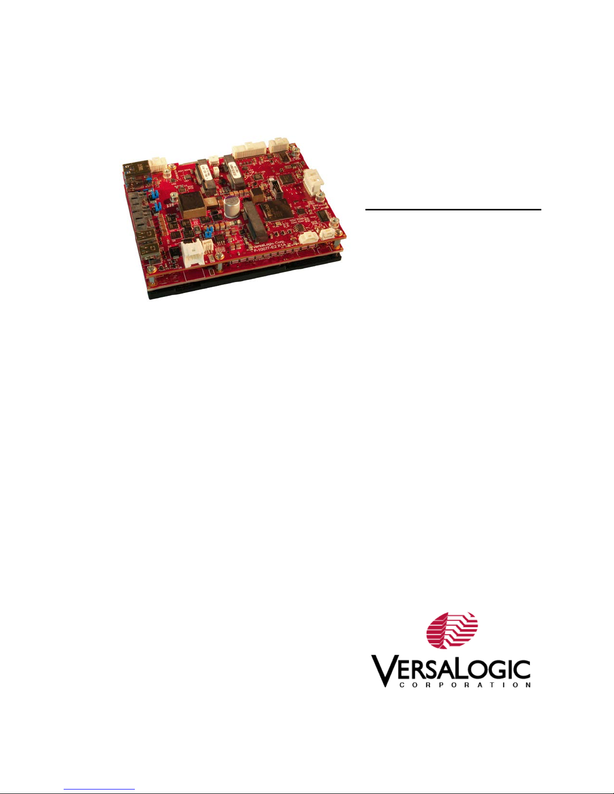
Blackbird
Manual
(VL-EPU-4562)
Intel® Core™-based Embedded
Processing Unit with SATA,
Dual Ethernet, USB, Digital I/O,
Serial, Video, Mini PCIe
Sockets, SPX, Trusted Platform
Module.
Page 2

WWW.VERSALOGIC.COM
12100 SW Tualatin Road
Tualatin, OR 97062-7341
(503) 747-2261
Fax (971) 224-4708
Copyright © 2017-2018 VersaLogic Corp. All right s r eser ved.
Notice:
Although every effort has been made to ensure this document is error-free, VersaLogic makes no
representations or warranties with respect to this product and specifically disclaims any implied warranties
of merchantability or fitness for any particular purpose.
VersaLogic reserves the right to revise this product and associated documentation at any time without
obligation to notify anyone of such changes.
PC/104, PC/104-Plus, and the PC/104 logo are trademarks of the PC/104 Consortium.
* Other names and brands may be claimed as the property of others.
EPU-4562 Programmer’s Reference Manual ii
Page 3

Product Release Notes
Release 1.1
Updated Uartmode1 – Uart Mode Register #1 section
Release 1.0
Initial Release.
Support
The EPU-4562 support page contains additional information and resources for this product
including:
Reference Manual (PDF format)
Operating system information and software drivers
Data sheets and manufacturers’ links for chips used in this product
BIOS information and upgrades
Utility routines and benchmark software
The VersaTech KnowledgeBase is an invaluable resource for resolving technical issues with
your VersaLogic product.
VersaTech KnowledgeBase
EPU-4562 Programmer’s Reference Manual iii
Page 4

Contents
Introduction ................................................................................................................... 1
Related Documents ............................................................................................................. 1
System Resources ........................................................................................................ 2
Interrupts ............................................................................................................................. 2
FPGA I/O Space ................................................................................................................. 2
FPGA Registers ............................................................................................................. 4
Register Access Key ........................................................................................................... 4
Reset Status Key ................................................................................................................. 4
FPGA Register Map ........................................................................................................... 5
FPGA Register Descriptions............................................................................................... 8
Product Information Registers ............................................................................... 8
BIOS and Jumper Status Register .......................................................................... 9
Timer Registers .................................................................................................... 10
Miscellaneous FPGA Registers ........................................................................... 13
SPI Control Registers .......................................................................................... 18
SPI Data Registers ............................................................................................... 20
SPI Debug Control Register and mSATA/PCIe Select Control Register ............ 21
ADM – ADC Control/Status Register ................................................................. 21
This register is used as the interrupt control/status register for the TI ADS8668A
and is primarily related to the ALARM signal output from the A/D. ................. 21
FANCON – Fan Control Register ....................................................................... 31
FANTACHLS, FANTACHMS – FANTACH Status Registers .......................... 32
Programming Information f or Hardware Interfaces .................................................. 41
Watchdog Timer ............................................................................................................... 41
Programmable LED .......................................................................................................... 41
Processor WAKE# Capabilities........................................................................................ 42
Tables
Table 1: FPGA I/O Map ...................................................................................................... 3
Table 2: FPGA Register Map.............................................................................................. 5
Table 3: PCR – Product Code and LED Register ............................................................... 8
Table 4: PSR – Product Status Register .............................................................................. 8
Table 5: SCR –Status/Control Register .............................................................................. 9
Table 6: TICR – 8254 Timer Interrupt Control Register .................................................. 10
Table 7: TISR – 8254 Timer Interrupt Status Register ..................................................... 11
Table 8: TCR – 8254 Timer Control Register .................................................................. 12
Table 9: MISCSR1 – Misc. Control Register #1 .............................................................. 13
EPU-4562 Programmer’s Reference Manual iv
Page 5

Contents
Table 10: MISCSR2 – Misc. Control Register #2 ............................................................ 15
Table 11: MISCSR3 – Misc. Control Register #3 ............................................................ 16
Table 11: MISCSR4 – Misc. Control Register #4 ............................................................ 17
Table 12: SPI Interface Control Register .......................................................................... 18
Table 13: SPI Interface Status Register ............................................................................ 19
Table 14: SPI – SPI Debug Control Register .................................................................... 21
Table 18: DIODIR1 – Digital I/O 8-1 Direction Control Register ................................... 22
Table 19: DIODIR2 – Digital I/O 16-9 Direction Control Register ................................. 22
Table 20: DIOPOL1 – Digital I/O 8-1 Polarity Control Register ..................................... 23
Table 21: DIOPOL2 – Digital I/O 16-9 Polarity Control Register ................................... 23
Table 22: DIOOUT1 – Digital I/O 8-1 Output Control Register ...................................... 23
Table 23: DIOOUT2 – Digital I/O 16-9 Output Control Register .................................... 23
Table 24: DIOIN1 – Digital I/O 8-1 Input Status Register ............................................... 24
Table 25: DIOIN2 – Digital I/O 16-9 Input Status Register ............................................. 24
Table 26: DIOIMASK1 – Digital I/O 8-1 Interrupt Mask Register .................................. 24
Table 27: DIOIMASK2 – Digital I/O 16-9 Interrupt Mask Register ................................ 24
Table 28: DIOISTAT1 – Digital I/O 8-1 Interrupt Mask Register ................................... 24
Table 29: DIOISTAT2 – Digital I/O 16-9 Interrupt Mask Register ................................. 25
Table 30: DIOCR – Digital I/O Control Register ............................................................. 25
Table 31: AUXDIR – AUX GPIO Direction Control Register ........................................ 26
Table 32: AUXPOL – AUX GPIO Polarity Control Register .......................................... 26
Table 33: AUXOUT – AUX GPIO Output Control Register ........................................... 27
Table 34: AUXIN – AUX GPIO Input Status Register .................................................... 27
Table 35: AUXICR – AUX GPIO Interrupt Mask Register ............................................. 27
Table 36: AUXISTAT – AUX GPIO Interrupt Status Register ........................................ 27
Table 37: AUXMODE1 – AUX I/O Mode Register ........................................................ 28
Table 38: WDT_CTL – Watchdog Control Register ........................................................ 29
Table 39: WDT_VAL – Watchdog Control Register ....................................................... 30
Table 40: XCVRMODE – COM Transceiver Mode Register .......................................... 30
Table 41: AUXMODE2 - AUX I/O Mode Register #2 .................................................... 31
Table 41: FANCON – Fan Control Register .................................................................... 32
Table 41: FANTACHLS – FANTACH Status Register LS Bits ...................................... 33
Table 41: FANTACHMS – FANTACH Status Register MS Bits.................................... 33
Table 42: UART1CR – UART1 Control Register (COM1) ............................................. 34
Table 43: UART2CR – UART2 Control Register (COM2) ............................................. 35
Table 43: UART3CR – UART3 Control Register (COM3) ............................................. 36
Table 43: UART4CR – UART4 Control Register (COM4) ............................................. 37
Table 44: UARTMODE1 – UART MODE Register #1 ................................................... 39
Table 45: UARTMODE2 – UART MODE Register #2 ................................................... 40
EPU-4562 Programmer’s Reference Manual v
Page 6

1
This document provides information for users requiring register-level information for developing
applications with the VL-EPU-4562.
Related Documents
The following documents are available on the EPU-4562 Product Support Web Page:
VL-EPU-4562 Hardware Reference Manual – provides information on the board’s hardware
features including connectors and all interfaces.
Introduction
Operating System compatibility and software package downloads are available at the
Software Support page.
VersaLogic
EPU-4562 Programmer’s Reference Manual 1
Page 7

2
Interrupts
The LPC SERIRQ is used for interrupt interface to the Skylake SoC.
Each of the following devices can have an IRQ interrupt assigned to it and each with an interrupt
enable control for IRQ3, IRQ4, IRQ5, IRQ6, IRQ7, IRQ9, IRQ10, and IRQ11:
8254 timers (with three interrupt status bits)
8x GPIOs (with one interrupt status bit per GPIO)16x Digital I/Os (with 1 interrupt status bit
per GPIO)
COM 1 UART (with 16550 interrupt status bits)
COM 2 UART (with 16550 interrupt status bits)
COM 3 UART (with the usual 16550 interrupt status bits).
System Resources
COM 4 UART (with the usual 16550 interrupt status bits).
Watchdog timer (one status bit)
Common interrupts can be assigned to multiple devices if software can deal with it (this is
common on UARTs being handled by a common ISR).
Interrupt status bits for everything except the UARTs will “stick” and are cleared by a “writeone” to a status register bit. The 16550 UART interrupts behave as defined for the 16550
registers and are a pass-through to the LPC SERIRQ.
Per the VersaAPI standard, anytime an interrupt on the SERIRQ is enabled, the slot becomes
active. All interrupts in the SERIRQ are high-true so when the slot becomes active, the slot will
be low when there is no interrupt and high when there is an interrupt.
FPGA I/O Space
The FPGA is mapped into I/O space on the LPC bus. The address range is mapped into a 64 byte
I/O window.
FPGA access: LPC I/O space
FPGA access size: All 8-bit byte accesses (16-bit like registers are aligned on 16-bit word
boundaries to make word access possible in software but the LPC bus still splits the accesses
into two 8-bit accesses)
FPGA address range: 0x1C80 to 0x1CBF (a 64-byte window)
The three 8254 timers only require four bytes of addressing and are located at the end of the
64-byte I/O block. The only requirement is that the base address must be aligned on a 4-byte
block. The table below lists the FPGA’s I/O map.
EPU-4562 Programmer’s Reference Manual 2
Page 8

Table 1: FPGA I/O Map
0x1C80 – 0x1CBB
FPGA registers
60 bytes
0x1CBC – 0x1CBF
8254 timer address registers
4 bytes
Address Range Device Size
System Resources and Maps
EPU-4562 Programmer’s Reference Manual 3
Page 9

Key:
R/W
Read/Write
RO
Read-Only
R/WC
Read-Status/Write-1-to-Clear
WO
Write-Only
ROC
Read-Only and clear-to-0 after reading
RSVD
Not implemented. Returns 0 when read. Writes are
ignored
• If AUX_PSEN is a '0' in MISCSR1 (default setting), then this is the same as the Platform reset.
If AUX_PSEN is programmed to a '1' , then it is the same as the Power-On Reset (POR).
3
This chapter describes the FPGA registers.
Table 2 (beginning on the following page) lists all 64 FPGA registers
Table 3 (refer to page 8) through Table 48 provide bit-level information on the individual
FPGA registers
Register Access Key
FPGA Registers
Reset Status Key
POR Power-on reset (only resets one time when input power comes on)
Platform Resets prior to the process or entering the S0 power state (that is, at power-on and in sleep states)
resetSX
n/a Reset doesn't apply to status or reserved registers
•
Reset Status Key
EPU-4562 Programmer’s Reference Manual 4
Page 10
EPU-4562 Programmer’s Reference Manual 5
FPGA Register Map
Table 2: FPGA Register Map
I/O
Address
Offset
Reset
D7
D6
D5
D4
D3
D2
D1
D0
C80
0
Platform
PLED
PRODUCT_CODE
C81
1
n/a
REV_LEVEL
EXTEMP
CUSTOM
BETA
C82
2
Platform
BIOS_JMP
BIOS_OR
BIOS_SEL
LED_DEBUG
WORKVER
0
WP_JMP
WP_EN
C83
3
Platform
IRQEN
IRQSEL2
IRQSEL1
IRQSEL0
0
IMASK_TC5
IMASK_TC4
IMASK_TC3
C84
4
Platform
INTRTEST
TMRTEST
TMRIN4
TMRIN3
0
ISTAT_TC5
ISTAT_TC4
ISTAT_TC3
C85
5
Platform
TIM5GATE
TIM4GATE
TIM3GATE
TM45MODE
TM4CLKSEL
TM3CLKSEL
TMROCTST
TMRFULL
C86
6
n/a 0 0 0 0 0 0 0 0
C87
7
n/a 0 0 0 0 0 0 0 0
C88
8
Platform
CPOL
CPHA
SPILEN1
SPILEN0
MAN_SS
SS2
SS1
SS0
C89
9
Platform
IRQSEL1
IRQSEL0
SPICLK1
SPICLK0
HW_IRQ_EN
LSBIT_1ST
HW_INT
BUSY
C8A
A
Platform
msb
<============>
lsb
C8B
B
Platform
msb
<============>
lsb
C8C
C
Platform
msb
<============>
lsb
C8D
D
Platform
msb
<============>
lsb
C8E
E
Platform 0 MUXSEL2
MUXSEL1
MUXSEL0
0
SERIRQEN
SPILB
DACLDA
C8F
F
Platform
IRQEN
IRQSEL2
IRQSEL1
IRQSEL0
ADC_RESET
IN_ALARM
ISTAT_ALARM
IMASK_ALAR
M
C90
10
POR 0 0 0 0
MINI3_PSDIS
MINI2_PSDIS
AUX_PSEN
MINI1_PSDIS
C91
11
POR
USB_HUBMOD
E
W_DISABLE
USB_HUBDIS
ETH0_OFF
USB2_OC2
USB2_OC1
USB2_DIS2
USB2_DIS1
C92
12
Platform
PROCHOT
LVDS_OC 0 0 0 PBRESET
0
TPM_PP
C93
13
POR 0 0
USB3_OC2
USB3_OC1 0 0
USB3_DIS2
USB3_DIS1
C94
14
resetSX
DIR_DIO8
DIR_DIO7
DIR_DIO6
DIR_DIO5
DIR_DIO4
DIR_DIO3
DIR_DIO2
DIR_DIO1
C95
15
resetSX
DIR_DIO16
DIR_DIO15
DIR_DIO14
DIR_DIO13
DIR_DIO12
DIR_DIO11
DIR_DIO10
DIR_DIO9
C96
16
resetSX
POL_DIO8
POL_DIO7
POL_DIO6
POL_DIO5
POL_DIO4
POL_DIO3
POL_DIO2
POL_DIO1
C97
17
resetSX
POL_DIO16
POL_DIO15
POL_DIO14
POL_DIO13
POL_DIO12
POL_DIO11
POL_DIO10
POL_DIO9
C98
18
resetSX
OUT_DIO8
OUT_DIO7
OUT_DIO6
OUT_DIO5
OUT_DIO4
OUT_DIO3
OUT_DIO2
OUT_DIO1
C99
19
resetSX
OUT_DIO16
OUT_DIO15
OUT_DIO14
OUT_DIO13
OUT_DIO12
OUT_DIO11
OUT_DIO10
OUT_DIO9
C9A
1A
n/a
IN_DIO8
IN_DIO7
IN_DIO6
IN_DIO5
IN_DIO4
IN_DIO3
IN_DIO2
IN_DIO1
C9B
1B
n/a
IN_DIO16
IN_DIO15
IN_DIO14
IN_DIO13
IN_DIO12
IN_DIO11
IN_DIO10
IN_DIO9
Page 11
FPGA Registers
EPU-4562 Programmer’s Reference Manual 6
I/O
Address
Offset
Reset
D7
D6
D5
D4
D3
D2
D1
D0
C9C
1C
Platform
IMASK_DIO8
IMASK_DIO7
IMASK_DIO6
IMASK_DIO5
IMASK_DIO4
IMASK_DIO3
IMASK_DIO2
IMASK_DIO1
C9D
1D
Platform
IMASK_DIO16
IMASK_DIO15
IMASK_DIO14
IMASK_DIO13
IMASK_DIO12
IMASK_DIO11
IMASK_DIO10
IMASK_DIO9
C9E
1E
Platform
ISTAT_DIO8
ISTAT_DIO7
ISTAT_DIO6
ISTAT_DIO5
ISTAT_DIO4
ISTAT_DIO3
ISTAT_DIO2
ISTAT_DIO1
C9F
1F
Platform
ISTAT_DIO16
ISTAT_DIO15
ISTAT_DIO14
ISTAT_DIO13
ISTAT_DIO12
ISTAT_DIO11
ISTAT_DIO10
ISTAT_DIO9
CA0
20
Platform
IRQEN
IRQSEL2
IRQSEL1
IRQSEL0 0 0 0 TMREN
CA1
21
resetSX
DIR_GPIO8
DIR_GPIO7
DIR_GPIO6
DIR_GPIO5
DIR_GPIO4
DIR_GPIO3
DIR_GPIO2
DIR_GPIO1
CA2
22
resetSX
POL_GPIO8
POL_GPIO7
POL_GPIO6
POL_GPIO5
POL_GPIO4
POL_GPIO3
POL_GPIO2
POL_GPIO1
CA3
23
resetSX
OUT_GPIO8
OUT_GPIO7
OUT_GPIO6
OUT_GPIO5
OUT_GPIO4
OUT_GPIO3
OUT_GPIO2
OUT_GPIO1
CA4
24
n/a
IN_GPIO8
IN_GPIO7
IN_GPIO6
IN_GPIO5
IN_GPIO4
IN_GPIO3
IN_GPIO2
IN_GPIO1
CA5
25
Platform
IMASK_GPIO8
IMASK_GPIO7
IMASK_GPIO6
IMASK_GPIO5
IMASK_GPIO4
IMASK_GPIO3
IMASK_GPIO2
IMASK_GPIO1
CA6
26
Platform
ISTAT_GPIO8
ISTAT_GPIO7
ISTAT_GPIO6
ISTAT_GPIO5
ISTAT_GPIO4
ISTAT_GPIO3
ISTAT_GPIO2
ISTAT_GPIO1
CA7
27
resetSX
MODE_GPIO8
MODE_GPIO7
MODE_GPIO6
MODE_GPIO5
MODE_GPIO4
MODE_GPIO3
MODE_GPIO2
MODE_GPIO1
CA8
28
Platform
IRQEN
IRQSEL2
IRQSEL1
IRQSEL0
0
RESET_EN
WDT_EN
WDT_STAT
CA9
29
Platform
msb
<============>
lsb
CAA
2A
Platform 0 0 0 0
COM4_MODE
COM3_MODE
COM2_MODE
COM1_MODE
CAB
2B
Platform
IRQEN
IRQSEL2
IRQSEL1
IRQSEL0 0 0 0 0
CAC
2C
Platform
COM_MODE 0 0 0 0 0 0
FAN_OFF
CAD
2D
n/a 0 0 0 0 0 0 0 0
CAE
2E
Platform
msb
<============>
lsb
CAF
2F
Platform
msb
<============>
lsb
CB0
30
n/a 0 0 0 0 0 0 0 0
CB1
31
n/a 0 0 0 0 0 0 0 0
CB2
32
Platform
IRQEN
IRQSEL2
IRQSEL1
IRQSEL0
UART1_BASE
3
UART1_BASE
2
UART1_BASE
1
UART1_BASE0
CB3
33
Platform
IRQEN
IRQSEL2
IRQSEL1
IRQSEL0
UART2_BASE
3
UART2_BASE
2
UART2_BASE
1
UART2_BASE0
CB4
34
Platform
IRQEN
IRQSEL2
IRQSEL1
IRQSEL0
UART3_BASE
3
UART3_BASE
2
UART3_BASE
1
UART3_BASE0
CB5
35
Platform
IRQEN
IRQSEL2
IRQSEL1
IRQSEL0
UART4_BASE
3
UART4_BASE
2
UART4_BASE
1
UART4_BASE0
CB6
36
Platform
UART4_485ADC
UART3_485ADC
UART2_485ADC
UART1_485ADC
UART4_EN
UART3_EN
UART2_EN
UART1_EN
CB7
37
Platform 0 0 0 0 0 0 0 FAST_MODE
CB8
38
n/a 0 0 0 0 0 0 0 0
CB9
39
n/a 0 0 0 0 0 0 0 0
CBA
3A
n/a 0 0 0 0 0 0 0 0
Page 12
FPGA Registers
EPU-4562 Programmer’s Reference Manual 7
I/O
Address
Offset
Reset
D7
D6
D5
D4
D3
D2
D1
D0
CBB
3B
n/a 0 0 0 0 0 0 0 0
CBC
3C
Platform
msb
<============>
lsb
CBD
3D
Platform
msb
<============>
lsb
CBE
3E
Platform
msb
<============>
lsb
CBF
3F
Platform
msb
<============>
lsb
Page 13
Key:
R/W
Read/Write
RO
Read-Only
R/WC
Read-Status/Write-1-to-Clear
WO
Write-Only
ROC
Read-Only and clear-to-0 after reading
RSVD
Not implemented. Returns 0 when read. Writes are
ignored
6-0
PRODUCT_CODE
0010011
Product Code for the EPU-4562 (0x13)
status bit (bit 0) i s set to ‘1’
1 – Custom Product or P LD/ F PGA
0 – Production
FPGA Register Descriptions
PRODUCT INFORMATION REGISTERS
This register drives the PLED on the paddleboard. It also provides read access to the product
code.
Table 3: PCR – Product Code and LED Register
Bit Identifier Access Default Description
7 PLED R/W 0
RO
Drives the programm abl e LED on the paddleboard.
0 – LED is off (default)
1 – LED is on
Table 4: PSR – Product Status Register
Bit Identifier Access Default Description
Revision level of the PLD (incremented every FPGA release)
7:3 REV_LEVEL[4:0]
2 EXTEMP
1 CUSTOM
0 BETA
RO
RO
RO
RO
N/A
N/A
N/A
N/A
0 – Indicates production rel ease revision level when BETA
status bit (bit 0) i s set to ‘0’
1 – Indicates development release revision level when BETA
Extended or Standard Temp Status (set via external resistor):
0 – Standard Temp
1 – Extended Temp (always set)
Custom or Standard Product Status (set in FPGA):
0 – Standard Product
Beta or Production Status (set in FPGA):
1 – Beta (or Debug)
EPU-4562 Programmer’s Reference Manual 8
Page 14
BIOS AND JUMPER STATUS REGISTER
external jumper is installed.
1 – BIOS Select will fol l ow the B I O S _SEL register setting
‘1’ for this to have any affect.
1 – LED is on
2
N/A
Reserved. Writes are ignored; reads always return 0.
1 – write protected (drives output low)
Table 5: SCR –Status/Control Register
Bit Identifier Access Default Description
7 BIOS_JMP RO N/A Status of the external BIOS s witch (jumper):
1 – Primary BIOS sel ected (the one on the COM Module)
0 – Backup BIOS sel ected (the one on the base board)
Note: For this implementation this reads the status of the jumper
all the time is es sentially the “AND” of the jumper sett i ng and (if
the BIOS_OR is set t o a ‘ 1’ ) the BIOS_SEL setting. Note that i f
BIOS_SEL sets a ‘ 1’ but a ‘ 0’ i s read here then that means the
6 BIOS_OR R/W 0 BIOS Switch (jumper) Override
0 – BIOS Select will f ol l ow the BI O S _JMP switch setting (FPGA
BIOS_SEL setting has no affect)
5 BIOS_SEL R/W 0 BIOS Select (see BIOS_OR):
0 – Primary BIOS sel ected (the one on the COM Module)
1 – Backup BIOS sel ected (the one on the base board)
Note: If the external BIOS configuration jumper is set to Backup
then setting this will not have any affect. The jumper must not be
installed to use this selection mode. Must have BIOS_OR set to a
FPGA Registers
Debug LED (controls the yellow LED):
LED_DEBUG
4
WORKVER
3
RESERVED RO
1 WP_JMP RO N/A Back-up BI O S Write protect jumper s t atus. WP_EN has to be set
0 WP_EN R/W 0 Back-up BIOS Write protect control. It drives an open-drain
R/W
RO
0
N/A
0 – LED is off and follows it s pri mary function (MSATA_DAS)
Status used to indic at e that the FPGA is not official l y released
and is still in a working state.
0 – FPGA is released
1 – FPGA is in a working stat e (not rel eased)
to a ‘0’ to read the actual jumper.
0 – Jumper is inst al l ed (write-protect is enabled)
1 – Jumper is removed (not write prot ected)
output.
0 – not write protected (open-drain output is Hi-Z so WP jumper
can be read)
EPU-4562 Programmer’s Reference Manual 9
Page 15
FPGA Registers
1 – Interrupts enabled
111 – IRQ11
1 – Interrupt enabled
1 – Interrupt enabled
TIMER REGISTERS
The FPGA implements an 8254-compatible timer/counter that includes three 16-bit timers.
Table 6: TICR – 8254 Timer Interrupt Control Register
Bit Identifier Access Default Description
8254 Timer interrupt enable/dis abl e:
7 IRQEN
6-4 IRQSEL(2:0)
R/W
R/W
0
000
0 – Interrupts disabled
8254 Timer interrupt IRQ select in LPC SERIRQ:
000 – IRQ3
001 – IRQ4
010 – IRQ5
011 – IRQ10
100 – IRQ6
101 – IRQ7
110 – IRQ9
3 RESERVED
2 IMASK_TC5
1 IMASK_TC4
0 IMASK_TC3
RO
R/W
R/W
R/W
0 Reserved. Writes are ignored; reads always return 0.
8254 timer #5 interrupt mask:
0
0 – Interrupt disabled
8254 timer #4 interrupt mask:
0
0 – Interrupt disabled
1 – Interrupt enabled
8254 timer #3 interrupt mask:
0
0 – Interrupt disabled
EPU-4562 Programmer’s Reference Manual 10
Page 16

Table 7: TISR – 8254 Timer Interrupt Status Register
7
RESERVED
0
Reserved. Writes are ignored; reads always return 0.
6
RESERVED
0
Reserved. Writes are ignored; reads always return 0.
5
RESERVED
0
Reserved. Writes are ignored; reads always return 0.
4
RESERVED
0
Reserved. Writes are ignored; reads always return 0.
3
RESERVED
0
Reserved. Writes are ignored; reads always return 0.
1 level
Bit Identifier Access Default Description
RO
RO
RO
RO
RO
Status for the 8254 Timer #5 output (terminal count) interrupt
when read. This bit is read-status and a write-1-to-clear.
2 ISTAT_TC5
1 ISTAT_TC4
RW/C
RW/C
N/A
N/A
0 – Timer output (terminal count) has not transitioned from 0 to
a 1 level
1 – Timer output (term i nal count) has transitioned from a 0 to a
1 level
Status for the 8254 Timer #4 output (terminal count) interrupt
when read. This bit is read-status and a write-1-to-clear.
0 – Timer output (term i nal count) has not transitioned from 0 to
a 1 level
1 – Timer output (term i nal count) has transitioned from a 0 to a
FPGA Registers
0 ISTAT_TC3
RW/C
N/A
Status for the 8254 Timer #3 output (terminal count) interrupt
when read. This bit is read-status and a write-1-to-clear.
0 – Timer output (term i nal count) has not transitioned from 0 to
a 1 level
1 – Timer output (term i nal count) has transitioned from a 0 to a
1 level
EPU-4562 Programmer’s Reference Manual 11
Page 17

Table 8: TCR – 8254 Timer Control Register
internal clocking.
internal clocking
Timer #5 is always on internal cl ock if configured as a 16-bit clock
registers (for example, OCTC4 with TMR4GATE ) for continuity testing.
0
TMRFULL
0
This bit can be read or written to, but i t has no function.
Bit Identifier Access Default Description
Debug/Test Only: Controls the “gate” signal on 8254 timer #5 when not
using an external gate signal:
7 TMR5GATE
6 TMR4GATE
5 TMR3GATE
R/W
R/W
R/W
0 – Gate on signal GCTC5 is disabl ed
0
1 – Gate on signal GCTC5 is enabled
Always set to 0 when configuring timer modes except when TMRFULL
is ‘0’ and then it should be set to ‘1’ and not changed unless using
Debug/Test Only: Controls the “gate” signal on 8254 timer #4 when not
using an external gate signal:
0 – Gate on signal GCTC4 is disabl ed
0
1 – Gate on signal GCTC4 is enabled
Always set to 0 when configuring timer modes except when TMRFULL
is ‘0’ and then it should be set to ‘1’ and not changed unless using
internal clocking
Debug/Test Only: Controls the “gate” signal on 8254 timer #3 when not
using an external gate signal:
0 – Gate on signal GCTC3 is disabl ed
0
1 – Gate on signal GCTC3 is enabled
Always set to 0 when configuring timer modes except when TMRFULL
is ‘0’ and then it should be set to ‘1’ and not changed unless using
FPGA Registers
4 TM45MODE
3 TM4CLKSEL
2 TM3CLKSEL
1 TMROCTST
R/W
R/W
R/W
R/W
R/W
Mode to set timers #4 and #5 i n:
0 – Timer #4 and #5 form one 32-bit timer controlled by timer #1 s i gnal s
1 – Timer #4 and Timer #5 are separate 16-bit timers with their own
0
control signals.
Almost always used in 32-bit mode especially when TMRFULL is a ‘0’
(the 16-bit timer #5 if of l i mited use)
Timer #4 Clock Selec t :
0 – Use internal 4.125 MHz clock (deri ved f rom LPC clock)
0
1 – Use external ICTC4 assigned to digital I/O
Timer #3 Clock Selec t :
0
0 – Use internal 4.125 MHz clock (deri ved f rom LPC clock)
1 – Use external ICTC3 assigned to digital I/O
Debug/Test Only: Used to derive OCTCx outputs with T I MxGATE
signals for continuit y t esting only:
0
0 – Normal operation
1 – Drive OCTCx outputs with corresponding TMRxGATE control
EPU-4562 Programmer’s Reference Manual 12
Page 18

FPGA Registers
power control signal and the inverse of MINI2_PSDIS.
AUX_PSEN
power control signal and the inverse of MINI1_PSDIS.
MISCELLANEOUS FPGA REGISTERS
MISCSR1 – Miscellaneous Control Regi st er #1
This is a register in the always-on power well of the FPGA. It holds its state during sleep modes
and can only be reset by a power cycle. This is a placeholder register for features like pushing the
power-button and also for software initiated resets should those be needed.
Reset: This register is only reset by the main power-on reset since it must maintain its state in
Sleep modes (for example, S3).
Table 9: MISCSR1 – Misc. Control Register #1
Bits Identifier Access Default Description
7-4 Reserved
2 MINI2_PSDIS
RO
R/W
00000 Reserved. Writes are ignored; reads always return 0.
Minicard #2 3.3 V power disable
0 – Minicard 3.3 V power stays on always (this is normally how
minicards operate if they support any Wake events)
0
1 – Minicard 3.3 V power will be turned off when not in S0 (in sleep
modes).
The Minicard 3.3 V power switch is control l ed by t he “OR” of the S0
1 AUX_PSEN
0 MINI1_PSDIS
R/W
R/W
CBR-4005B 8xGPIO (sometimes called “AUX” GPIOs) I/O Power
Enable
0 – The GPIO pullups will be powered down in sleep modes (onl y
power in S0)
1 – The GPIO pullups will not be powered down in sleep m odes
0
and the configuration will remain.
This power is used for both the GPIO pul l up voltage and for the
3.3V power on Pin 37 of the User Interface connector J2.
Note: Some register resets are conditional on the state of
Minicard #1 3.3 V power disable
0 – Minicard 3.3 V power stays on always (this is normally how
minicards operate if they support any Wake events)
0
1 – Minicard 3.3 V power will be turned off when not in S0 (in sleep
modes).
The Minicard 3.3 V power switch is control l ed by t he “OR” of the S0
EPU-4562 Programmer’s Reference Manual 13
Page 19

FPGA Registers
MISCSR2 – Miscellaneous Control Regi st er #2
This is a register in the always-on power well of the FPGA. It holds its state during sleep modes
and can only be reset by a power cycle. It is primarily used for control signals for the alwayspowered Ethernet controllers and the USB hubs. This register is only reset by the main power-on
reset since it must maintain its state in sleep modes (for example, S3).
EPU-4562 Programmer’s Reference Manual 14
Page 20

Table 10: MISCSR2 – Misc. Control Register #2
when entering all sleep modes). USB port s cannot be used to wake-up
at power on.
then a ‘0’
then a ‘0’
then a ‘0’
Bit
Identifier
USB_HUBMODE
7
6 W_DISABLE
5 USB_HUBDIS
Access Default
R/W
R/W
R/W
0
0
0
Description
Determines whether the hub resets onl y onc e (to support wake-up from
sleep modes on USB ports ) or resets every time it enters sleep modes
using the platform res et :
0 – USB Hub will be reset once at power on. Use USB_HUBDIS to
manually control the reset i f necessary. This supports USB Wake-up
modes
1 – USB Hub will be reset by platform reset every time (will be reset
Controls the W_DI SABLE (Wireless Dis abl e) signal going to the PCIe
Minicards (disables both minicards if asserted):
0 – W_DISAB LE signal is not asserted (Enabled)
1 – W_DISAB LE signal is asserted (Disabled)
Note: There are other control s ourc es that can be configured to control
this signal and if enabled the control becomes the “OR” of all sources
Control the reset on the USB2513B Hub (used for 3x Minicard USB
ports).
0 – USB2513 Hub is Enabled (reset released)
1 – USB2513 Hub is in Reset
Note: FPGA was changed so t hat Platform reset drives this res et once
FPGA Registers
4 ETHOFF0
3 USB2_OC2
2 USB2_OC1
1 USB2_DIS2
R/W
RO
RO
R/W
Disables Ethernet control l er #0 (controls the ETH_OFF# input to the
I210-IT):
0
0 – Ethernet controller is enabl ed (On)
1 – Ethernet controller is di sabled (Off)
Overcurrent Status from the USB 2.0 port 2,3 VBUS power switches.
This signal also pass ed to the fourth USB_6_7_OC# input on the COM
Express connector.
0 – VBUS power switch is not in overcurrent (ei t her O K or di sabled)
N/A
1 – VBUS power switch is in overcurrent and is now off.
Note: The power switches latch-of f in overcurrent and can only be re-
enabled by a power-cycle or by setting this bit to a ‘1’, wait >1msec and
Overcurrent Status from the USB 2.0 port 0,1 VBUS power switches.
This signal also pass ed to the third USB_4_5_OC# input on the COM
Express connector.
0 – VBUS power switch is not in overcurrent (ei t her O K or di sabled)
N/A
1 – VBUS power switch is in overcurrent and is now off.
Note: The power switches latch-of f in overcurrent and can only be re-
enabled by a power-cycle or by setting this bit to a ‘1’, wait >1msec and
Disable control for the paddleboard USB 2. 0 ports 2,3 VBUS power
switches (there are two power-switches but they have a common power
enable and overcurrent status)
0 – VBUS power switches are enabled
0
1 – VBUS power switched are disabled.
Note: The power switches latch-of f in overcurrent and can only be re-
enabled by a power-cycle or by setting this bit to a ‘1’, wait >1msec and
EPU-4562 Programmer’s Reference Manual 15
Page 21

Bit
then a ‘0’
1 – THERMTRIP is as serted
1 – Overcurrent is asserted (power switch i s off)
1-0
Reserved
00
Reserved. Writes are ignored; reads always return 0.
Identifier
0 USB2_DIS1
Access Default
R/W
0
Description
Disable control for the paddleboard USB 2.0 ports 0,1 VBUS power
switches (there are two power-switches but they have a common power
enable and overcurrent status)
0 – VBUS power switches are enabled
1 – VBUS power switched are disabled.
Note: The power switches latch-of f in overcurrent and can only be re-
enabled by a power-cycle or by setting this bit to a ‘1’, wait >1msec and
MISCSR3 – Miscellaneous Control Regi st er #3
This register enables software to “push” the reset button.
Table 11: MISCSR3 – Misc. Control Register #3
Bits Identifier Access Default Description
The status of the THERMTRIP signal from the CPU module.
7 PROCHOT
RO
N/A
0 – THERMTRIP is not asserted (not hot)
FPGA Registers
6 LVDS_OC
3-5 Reserved
2 PBRESET
RO
RO
R/W
RO
N/A
N/A
---
The overcurrent status from the LVDS panel power switch. If this is
ever asserted, the LVDS panel enabl e s i gnal must be de-asserted
and then asserted to “unlatch” t he power fault condition on the
power switch.
0 – LVDS Overcurrent is not asserted
1 – LVDS Overcurrent is asserted
Reads the overcurrent status f or the USB paddleboard power
switches (there are two power switches for the four port s but they
have a common overcurrent st atus).
0 – Overcurrent is not assert ed (power switch i s on)
When written to, this will do the sam e thing as pushing the reset
button, which could be useful f or a software-initiated watchdog.
0 – No action
1 – Activate the reset push-button
Note: Because this generates a reset that will reset this register, it
isn’t likely a value of a ‘1’ can ever be read-back, so it is somewhat
“write-only”.
EPU-4562 Programmer’s Reference Manual 16
Page 22

FPGA Registers
6
RESERVED
RO 0 Reserved – Writes are i gnored. Reads always return 0
state and must be res t arted
3
RESERVED
RO 0 Reserved – Writes are i gnored. Reads always return 0
2
RESERVED
RO 0 Reserved – Writes are i gnored. Reads always return 0
1 – USB 3.0 VBUS power switch is di sabled
MISCSR4 – Miscellaneous Cont r ol Regi st er #4
This register is used to monitor the overcurrent status of the 2x USB 3.0 VBUS power switch.
Table 12: MISCSR4 – Misc. Control Register #4
Bits Identifier Access Default Description
7 RESERVED RO 0 Reserved – Writ es are ignored. Reads always return 0
5 USB3_OC2 RO N/A The status of the overc urrent signal on VBUS power switch for
4 USB3_OC1 RO N/A The status of the overc urrent signal on VBUS power switch for first
1 USB3_DIS2 R/W 0 Used to control the enable on VBUS power switc h f or second USB
0 USB3_DIS1 R/W 0 Used to control the enable on VB US power switch for first USB 3.0
second USB 3.0 Port 2. This signal also passed to the second
USB_2_3_OC# input on the COM Express connector.
0 – USB 3.0 VBUS power switch is operat i ng normally or it is
disabled
1 – USB 3.0 VBUS power switch is i n an overc urrent shutdown
state and must be res t arted
USB 3.0 Port 1. This si gnal al so passed to the first USB_0_1_OC#
input on the COM Express connector.
0 – USB 3.0 VBUS power switch is operat i ng normally or it is
disabled
1 – USB 3.0 VBUS power switch is i n an overc urrent shutdown
3.0 Port 2.
0 – USB 3.0 VBUS power switch is enabl ed
Port 1.
0 – USB 3.0 VBUS power switch is enabl ed
1 – USB 3.0 VBUS power switch is di sabled
EPU-4562 Programmer’s Reference Manual 17
Page 23

FPGA Registers
SPI clock polarit y – S ets the SCLK idle state.
1 – SCLK idles high
1 – Data is read on falling edge
bits SS[2:0]
SPI CONTROL REGISTERS
These are placed at the traditional offset 0x8 location. Only external SPX interface devices use
this interface. Because the board uses a 9-pin SPX connector, only two devices are supported.
SPICONTROL
Table 13: SPI Interface Control Register
Bit Identifier
7 CPOL
6 CPHA
5-4 SPILEN(1:0)
3 MAN_SS
2-0 SS(2:0)
Access Default
R/W 0
R/W 0
R/W 00
R/W 0
R/W 000
Description
0 – SCLK idles low
SPI clock phase – Sets the SCLK edge on which valid data will be read.
0 – Data is read on rising edge
Determines the SPI frame length. This selection works i n manual and
auto slave select m odes.
00 – 8-bit
01 – 16-bit
10 – 24-bit
11 – 32-bit
Determines whether the slave select lines are asserted through the
user software or are automatical l y as serted by a write to SPIDATA3.
0 - The slave select operates aut omatically
1 - The slave select line is controlled manually through SPICONTROL
SPI slave device selec t i on:
000 – None
001 – SS0#
010 – SS1#
011 – Undefined (ignored)
100 – Undefined (ignored)
101 – Undefined (ignored)
110 – Undefined (ignored)
111 – Undefined (ignored)
EPU-4562 Programmer’s Reference Manual 18
Page 24

FPGA Registers
group of eight interrupts.
1 - The IRQ can be asserted
external hardware interrupt is no longer present.
SPISTATUS
The SPX interrupt is not connected on this product. The control bits and status associated are
still defined in the register set but the SPX interrupt will always be de-asserted.
Table 14: SPI Interface Status Register
Bits Identifier Access Default Description
The SPX interrupt is not connect ed on t hi s product (always deasserted).
Selects which IRQ will be enabled if HW_IRQ_EN = 1. Interrupts are
not used on this board, so thi s j ust becomes a read/write nonfunctional field.
7-6 IRQSEL[1:0] R/W 00
5-4 SPICLK(1:0) R/W 00
3 HW_IRQ_EN R/W 0
00 – IRQ3
01 – IRQ4
10 – IRQ5
11 – IRQ10
Note: These are the firs t four interrupts in the “usual” LPC SERI RQ
Selects one of four SCLK frequencies. This is based on a 33 MHz
LPC clock.
00 – 0.75Mhz(24Mhz/32)
01 – 1.5 Mhz(24Mhz/16)
10 – 2 Mhz(24 Mhz/8)
11 – 6 Mhz (24Mhz/4)
The SPX interrupt is not connect ed on t hi s product (always de-
asserted).
This enables the select ed IRQ to be activated by a SPI device that is
configured to use its interrupt capability.
0 - IRQs are disabled for SPI operations.
Controls the SPI shif t direction from the SPIDATA (x) regist ers.
2 LSBIT_1ST R/W 0
1 HW_INT RO 0
0 BUSY
RO
N/A
0 - Data is left-shifted (MSB first).
1 - Data is right-shifted (LS B first)
SPX interrupt is not connected on t hi s product (always de-asserted).
Status flag which indicat es when the hardware SPX signal SINT# is
asserted.
0 - The hardware interrupt SINT# is de-asserted.
1 - An interrupt is present on S I NT #
If HW_IRQ_EN= 1, the selected IRQ will also be asserted by the
hardware interrupt. HW_INT is read-only and is cleared when the
Status flag which indicat es when an SPI transaction is underway. I2C
is so slow that there is no reas on t o ever pol l t hi s.
0 - The SPI bus is idle.
1 - SCLK is clocki ng data in/out of the SPIDATA(x) registers (t hat i s,
busy)
EPU-4562 Programmer’s Reference Manual 19
Page 25

FPGA Registers
SPI DATA REGISTERS
There are four data registers used on the SPI interface. How many are used depends on the
device being communicated with. SPIDATA0 is typically the least significant byte and
SPIDATA3 is the most significant byte. Any write to the most significant byte SPIDATA3
initiates the SCLK and, depending on the MAN_SS state, will assert a slave select to begin an
SPI bus transaction.
Data is sent according to the LSBIT_1ST setting. When LSBIT_1ST = 0, the MSbit of
SPIDATA3 is sent first and received data will be shifted in the LSbit of the selected frame size
determined by SPILEN1 and SPILEN0. When LSBIT_1ST = 1, the LSbit of the selected frame
size is sent first and the received data will be shifted in the MSbit of SPIDATA3.
SPIDATA0 (Least Significant Byte)
D7 D6 D5 D4 D3 D2 D1 D0
MSB LSB
SPIDATA1
D7 D6 D5 D4 D3 D2 D1 D0
MSB LSB
SPIDATA2
D7 D6 D5 D4 D3 D2 D1 D0
MSB LSB
SPIDATA3 (Most Signifi cant Byte) [Cycle Trigger Register]
D7 D6 D5 D4 D3 D2 D1 D0
MSB LSB
EPU-4562 Programmer’s Reference Manual 20
Page 26

FPGA Registers
7
Reserved
0
Reserved. Writes are ignored; reads always return 0.
mSATA/PCIe Mux selection for Minicard slot (and 2nd SATA
switches to the SATA c onnector.
console redirect using IRQ3).
Debug/Test Only: Used to loop SP I output data back to the input
active) 0 Reserved
0
Reserved. Writes are i gnored; reads always return 0.
7
IRQEN
R/W
ADC ALARM Interrupt Enable/Disabl e.
Note: This is ess entially the interrupt mask.
SPI DEBUG CONTROL REGISTER AND MSATA/PCIE SELECT CONTROL REGISTER
This register is only used to set an SPI loopback (debug/test only) but is also used for the
mSATA/PCIe Minicard Mux select.
Table 15: SPI – SPI Debug Control Register
Bit Identifier Access Default Description
RO
connector):
• 000 – Select mSAT A using only pin 43 (MSATA_DETECT). This
is an Intel-mode that i s rel i abl e for PCIe Minicards but not for
mSATA modules that inadvertently ground this signal.
• 001 – Use only Pin 51 (PRES_DISA B LE2#). This is the default
method and is defined in the Draf t mSATA spec but som e
Minicards use it as a sec ond wireles s disable.
6-4
MUXSEL(2:0)
R/W
000
• 010 – Use either Pin 43 or Pin 51. This will work just like 001
because Pin 43 is disabled by an FP G A pul l -down.
• 011 – Force PCIe mode on the Minic ard
• 100 – Force mSATA mode on the Minicard.
• 101 – Undefined (same as 000)
• 110 – Undefined (same as 000)
• 111 – Undefined (same as 000)
Note: When the Minic ard uses PCIe, the SATA channel automatically
3 Reserved
2 SERIRQEN
1 SPILB
RO
R/W
R/W
RO
ADM – ADC CONTROL/STATUS REGISTER
This register is used as the interrupt control/status register for the TI ADS8668A and is
primarily related to the ALARM signal output from the A/D.
Bit Identifier Access Default Description
0 Reserved. Writes are ignored; reads always return 0.
When an IRQ is as signed a slot in the SERIRQ, it will drive the s l ot
with the interrupt state, but this bit must be set to a ‘1’ t o do that.
0 – Slots assigned to SERIRQ are not driven (available for other
devices).
0
1 – Slots assigned to SERIRQ are driven with their current interrupt
state (which is low since interrupts are high-true).
This is because the defaul t interrupt settings in this FP GA can conflict
with other interrupts if the Vers aAPI is not being used (for example,
(debug/test mode).
0 – Normal operation
0
1 – Loop SPI output data back to the SPI input data (data output stil l
0
0 – Interrupts disabled
1 – Interrupts enabled.
EPU-4562 Programmer’s Reference Manual 21
Page 27

Bit Identifier Access Default Description
6-4
IRQSEL(2:0)
R/W
ADC ALARM Interrupt IRQ Select i n LP C SERIRQ:
FYI – same values are other products.
3
ADC_RESET
R/W
ADS8668A ADC RESET
reset will reset the A/D to a power-on reset s tate.
2
IN_ALARM
RO
Returns the ADS8668A ADC ALARM st atus value.
1 – ALARM is asserted
1
ISTAT_ALARM
RO
ADC ALARM interrupt status. A read returns the interrupt status.
assertion)
0
IMASK_ALARM
RW
ADC ALARM Interrupt Mask :
1 – Interrupt enabled.
1 – Output
Bits
Identifier
Access
Default
Description
1 – Output
000 – IRQ3
001 – IRQ4
010 – IRQ5
000
0
011 – IRQ10
100 – IRQ6
101 – IRQ7
110 – IRQ9
111 – IRQ11
0 – deassert reset (normal operation)
1 – assert reset
NOTE: Always assert this for >400nsec since the part has some
strange modes for shorter resets. Regardless a standard Platform
FPGA Registers
N/A
N/A
0
0 – ALARM is deasserted
Writing a ‘1’ will clear the interrupt status. This bit is set to a ‘1’ on
a transition from low-to-high of the ADC ALARM signal (alarm
0 – Interrupt disabled
DIODIRx (x=1,2) – Digital I /O Direction Control Registers
These two registers control the directions of the 16 digital I/O signals.
This reset depends on the state of the FPGA_PSEN signal. If FPGA_PSEN is a ‘0’ then the reset
is the power-on and Platform Reset. If FPGA_PSEN is a ‘1’ then this register is only reset at
power-on.
Table 16: DIODIR1 – Digital I/O 8-1 Direction Control Register
Bits Identifier Access Default Description
Sets the DIOx direction. For each bit:
7-0 DIR_DIO[8:1]
R/W
0x00
0 – Input
Table 17: DIODIR2 – Digital I/O 16-9 Direction Control Register
7-0 DIR_DIO[16:9]
R/W
EPU-4562 Programmer’s Reference Manual 22
0x00
Sets the DIOx direction. For each bit:
0 – Input
Page 28

FPGA Registers
1 – Invert polarity
1 – Invert polarity
1 – Asserts the output (1 i f polarity not-inverted, 0 if inverted)
DIOPOLx (x=1,2) – Digital I/O Polarity Control Registers
These two registers control the polarity of the 16 Digital I/O signals.
This reset depends on the state of the FPGA_PSEN signal. If FPGA_PSEN is a ‘0’ then the reset
is the power-on and Platform Reset. If FPGA_PSEN is a ‘1’ then this register is only reset at
power-on.
Table 18: DIOPOL1 – Digital I/O 8-1 Polarity Control Register
Bits Identifier Access Default Description
Sets the DIOx polarity. For eac h bi t:
7-0 POL_DIO[8:1]
R/W
0x00
0 – No polarity inversion
Table 19: DIOPOL2 – Digital I/O 16-9 Polarity Control Register
Bits Identifier Access Default Description
Sets the DIOx polarity. For eac h bi t:
7-0 POL_DIO[16:9]
R/W
0x00
0 – No polarity inversion
DIOOUTx (x=1,2) – Digital I / O Output Control Registers
These two registers set the DIO output value. This value will only set the actual output if the DIO
direction is set as an output. Reading this register does not return the actual input value of the
DIO (use the DIOIN register for that). As such, this register can actually be used to detect
input/output conflicts.
This reset depends on the state of the FPGA_PSEN signal. If FPGA_PSEN is a ‘0’ then the reset
is the power-on and Platform Reset. If FPGA_PSEN is a ‘1’ then this register is only reset at
power-on.
Table 20: DIOOUT1 – Digital I/O 8-1 Output Control Register
Bits Identifier Access Default Description
Sets the DIOx output. For each bit :
7-0 OUT_DIO[8:1]
R/W
0x00
0 – De-asserts the output (0 if polarity not invert ed, 1 i f inverted)
1 – Asserts the output (1 i f polarity not-inverted, 0 if inverted)
Table 21: DIOOUT2 – Digital I/O 16-9 Output Control Register
Bits Identifier Access Default Description
Sets the DIOx output. For each bit :
7-0 OUT_DIO[16:9]
R/W
0x00
0 – De-asserts the output (0 if polarity not invert ed, 1 i f inverted)
DIOINx (x=1,2) – Digital I/O Input Status Registers
These two registers set the DIO input value. It will read the input value regardless of the setting
on the direction (that is, it always reads the input). This reads the actual state of the DIO pin into
the part.
EPU-4562 Programmer’s Reference Manual 23
Page 29

FPGA Registers
de-asserted if polarity inverted
de-asserted if polarity inverted
1 – Interrupt enabled
Bits
Identifier
Access
Default
Description
(POL_DIOx=0) or high-to-low (POL_DIOx=1).
Table 22: DIOIN1 – Digital I/O 8-1 Input Status Register
Bits Identifier Access Default Description
Reads the DIO input stat us. For each bit:
7-0 IN_DIO[8:1]
RO
N/A
0 – Input de-asserted if polarity not-inverted;
as serted if polarity inverted
1 Input asserted if polarit y not-inverted;
Table 23: DIOIN2 – Digital I/O 16-9 Input Status Register
Bits Identifier Access Default Description
Reads the DIO input stat us. For each bit:
7-0 IN_DIO[16:9]
RO
N/A
DIOIMASKx (x=1,2) – Digital I/O Interrupt Mask Registers
These two registers are the interrupt mask registers for the digital IOs. The reset type is Platform
Reset because interrupts always have to be setup after exiting sleep states.
0 – Input de-asserted if polarity not-inverted;
as serted if polarity inverted
1 Input asserted if polarit y not-inverted;
Table 24: DIOIMASK1 – Digital I/O 8-1 Interrupt Mask Register
Bits Identifier Access Default Description
Digital I/O 8-1 interrupt mask. For each bit:
7-0 IMASK_DIO[8:1]
R/W
0
0 – Interrupt disabled
1 – Interrupt enabled
Table 25: DIOIMASK2 – Digital I/O 16-9 Interrupt Mask Register
Bits Identifier Access Default Description
Digital I/O 16-9 interrupt m ask. For each bit:
7-0
IMASK_DIO[16:9]
R/W
0
0 – Interrupt disabled
DIOISTATx (x=1,2) – Digital I/O Interrupt Status Registers
Table 26: DIOISTAT1 – Digital I/O 8-1 Interrupt Mask Register
DIOx interrupt status. A read returns the interrupt status. Writing
7-0 ISTAT_DIO[8:1]
RW/C
N/A
a ‘1’ clears the interrupt s t atus.
This bit is set t o a ‘ 1’ on a t ransition from low-to-high
EPU-4562 Programmer’s Reference Manual 24
Page 30

Table 27: DIOISTAT2 – Digital I/O 16-9 Interrupt Mask Register
(POL_DIOx=0) or high-to-low (POL_DIOx=1).
1 – Interrupts enabled
111 – IRQ11
3-1
RESERVED
000
Reserved. Writes are ignored; reads always return 0.
Bits Identifier Access Default Description
DIOx interrupt status. A read returns the interrupt status. Writing
7-0
ISTAT_DIO[16:9]
RW/C
N/A
a ‘1’ clears the interrupt s tatus.
This bit is set t o a ‘ 1’ on a t ransition from low-to-high
DIOCR – Digital I/O Control Register
One interrupt can be generated for the 16 digital I/Os. Reset type is Platform.
Table 28: DIOCR – Digital I/O Control Register
Bits Identifier Access Default Description
DIO interrupt enable/disable:
7 IRQEN
6-4 IRQSEL(2:0)
R/W
R/W
0
000
0 – Interrupts disabled
DIO interrupt IRQ select i n LPC SERIRQ:
000 – IRQ3
001 – IRQ4
010 – IRQ5
011 – IRQ10
100 – IRQ6
101 – IRQ7
110 – IRQ9
FPGA Registers
0 TMREN
RO
R/W
Timer enable signals (used to switch digital I/Os to timer control
signals):
0
0 – Timers disabled
1 – Timers enabled and some DIOs are used based on the
TMRFULL setting in the Timer control register (TCR)
EPU-4562 Programmer’s Reference Manual 25
Page 31

FPGA Registers
1 – Output
edge used.
AUXDIR – AUX GPIO Direction Control Register
This register controls the direction of the eight AUX GPIO signals.
This reset depends on the state of the FPGA_PSEN signal. If FPGA_PSEN is a ‘0’ then the reset
is the power-on and Platform Reset. If FPGA_PSEN is a ‘1’ then this register is only reset at
power-on.
Table 29: AUXDIR – AUX GPIO Direction Control Register
Bit Identifier Access Default Description
Sets the direction of the AUX GPIOx lines. For each bit:
7-0 DIR_GPIO[8:1]
R/W
0
0 – Input
AUXPOL – AUX GPIO Polarity Control Register
This register controls the polarity of the eight AUX GPIO signals.
This reset depends on the state of the FPGA_PSEN signal.
If FPGA_PSEN is a ‘0’ then the reset is the power-on and Platform Reset.
If FPGA_PSEN is a ‘1’ then this register is only reset at power-on.
Table 30: AUXPOL – AUX GPIO Polarity Control Register
Bits Identifier Access Default Description
Sets the polarity of the A UX GPIOx lines . For each bit:
0 – No inversion
7-0 POL_GPIO[8:1]
R/W
0
1 – Invert
Note: This impacts the polarity as well as the interrupt status
AUXOUT – AUX GPIO Output Control Register
This register sets the AUX GPIO output value. This value will only set the actual output if the
GPIO direction is set as an output. Reading this register does not return the actual input value of
the GPIO (use the AUXIN register for that). As such, this register can actually be used to detect
input/output conflicts.
This reset depends on the state of the FPGA_PSEN signal.
If FPGA_PSEN is a ‘0’ then the reset is the power-on and Platform Reset.
If FPGA_PSEN is a ‘1’ then this register is only reset at power-on.
EPU-4562 Programmer’s Reference Manual 26
Page 32

FPGA Registers
de-asserted if polarity inverted
1 – Interrupt enabled
Table 31: AUXOUT – AUX GPIO Output Control Register
Bits Identifier Access Default Description
Sets the AUX GPIOx output values. For eac h bi t :
7-0 OUT_GPIO[8:1]
R/W
0 – De-asserts the output (0 if polarity not-inverted, 1 if i nvert ed)
0
1 – Asserts the output (1 i f polarity not-inverted, 0 if inverted)
AUXIN – AUX GPIO I/O Input Status Regi st er
This register sets the AUX GPIO input value. It will read the input value regardless of the setting
on the direction (that is, it always reads the input). This reads the actual state of the GPIO pin
into the part.
Table 32: AUXIN – AUX GPIO Input Status Register
Bits Identifier Access Default Description
Reads the GPIOx input status. For each bit:
7-0 IN_GPIOIO[8:1]
RO
N/A
0 – Input de-asserted if polarity not-inverted;
as serted if polarity inverted
1 Input asserted if polarit y not -inverted;
AUXIMASK – AUX GPIO Interrupt Mask Register
This is the interrupt mask register for the AUX GPIOs and the interrupt enable selection. The
reset type is Platform Reset because interrupts always have to be setup after exiting sleep states.
Table 33: AUXICR – AUX GPIO Interrupt Mask Register
Bits Identifier Access Default Description
GPIOx interrupt mask. For each bit:
7-0
IMASK_GPIO[8:1]
R/W
0
0 – Interrupt disabled
AUXISTAT – AUX GPIO I/O Interrupt Status Register
Table 34: AUXISTAT – AUX GPIO Interrupt Status Register
Bits Identifier Access Default Description
GPIOx interrupt status. A read returns the interrupt status. Writing
7-0
ISTAT_GPIO[8:1]
RW/C
N/A
a ‘1’ clears the interrupt s tatus.
This bit is set t o a ‘ 1’ on a t ransition from low-to-high
(POL_DIOx=0) or high-to-low (POL_DIOx=1).
EPU-4562 Programmer’s Reference Manual 27
Page 33

AUXMODE1– AUX I/O Mode Register #1
Bit
Identifier
Access
Default
Description
1 – ICTC3 (input)
1 – OCTC3 (output)
1 – OCTC4 (output)
Setting GPIO polarity to ‘ 1’ makes it high-true.
The GPIO input status can still be read.
Setting GPIO polarity to ‘ 1’ makes it high-true.
‘1’ makes it high-true.
These two registers select the mode on each AUX GPIO.
This reset depends on the state of the FPGA_PSEN signal.
If FPGA_PSEN is a ‘0’ then the reset is the power-on and Platform Reset.
If FPGA_PSEN is a ‘1’ then this register is only reset at power-on.
Table 35: AUXMODE1 – AUX I/O Mode Register
GPIO8 mode.
7 MODE_GPIO8
6 MODE_GPIO7
5 MODE_GPIO6
R/W
R/W
R/W
0
0
0
0 – GPIO (I/O)
GPIO7 mode.
0 – GPIO (I/O)
1 – ICTC4 (input)
GPIO6 mode.
0 – GPIO (I/O)
FPGA Registers
4 MODE_GPIO5
3 MODE_GPIO4
2 MODE_GPIO3
1 MODE_GPIO2
0 MODE_GPIO1
R/W
R/W
R/W
R/W
R/W
GPIO5 mode.
0
0 – GPIO (I/O)
GPIO4 mode.
0 – GPIO (I/O)
1 – WDOG_RESET# (output only). In this mode, the GPIO will be
0
the FPGA watchdog timer trigger output that signals external
equipment that the watchdog fired.
The GPIO input status can still be read. Default is low-true.
GPIO3 mode.
0 – GPIO (I/O)
1 – WAKE# (i nput onl y). In this mode, the GPIO is pas sed
0
through to the PCI_WAKE# signal.
Default is low-true. Setting GP IO polarity to ‘1’ makes it high-true.
GPIO2 mode.
0 – GPIO (I/O)
1 – W_DISABLE# (input only). In this mode, the GPIO is passed
0
through to the W_DISABLE# signal.
The GPIO input status can still be read. Default is low-true.
GPIO1 mode.
0 – GPIO (I/O)
1 – SLEEP# (input only). This is the sleep s i gnal on the
0
baseboard power connector. It passes through the SLEEP# input
on the CPU module. Default is l ow-true. S etting GPIO polarity to
EPU-4562 Programmer’s Reference Manual 28
Page 34

WDT_CTL – Watchdog Control Register
1 – Interrupts enabled
111 – IRQ11
1 – Board will be reset if the Watchdog “fires”
Note:
a reset occurs
Reset type is Platform.
Table 36: WDT_CTL – Watchdog Control Register
Bits Identifier Access Default Description
Watchdog int errupt enable/disable:
7 IRQEN
6-4 IRQSEL(2:0)
R/W
R/W
0
000
0 – Interrupts disabled
Watchdog interrupt I RQ select in LPC SERIRQ:
000 – IRQ3
001 – IRQ4
010 – IRQ5
011 – IRQ10
100 – IRQ6
101 – IRQ7
110 – IRQ9
FPGA Registers
3 Reserved
2 RESET_EN
1 WDT_EN
0 WDT_STAT
RO
R/W
R/W
RO
0 Reserved. Writes are ignored; reads always return 0.
Enable the Watchdog to assert the push-button reset if i t “fires”.
0
0 – Watchdog will not reset the board
Watchdog Enable:
0 – Watchdog is disabled
0
1 – Watchdog is enabled
The WDT_VAL regis ter must be set before enabling.
Watchdog St at us:
0 – Watchdog disabled or watchdog has not “fired”
1 – Watchdog f i red.
Note: Once set to a ‘1’, it will remain so until any of the following
0
occurs:
• the WDT_VAL register is written to
• the WDT_EN is di sabled
•
EPU-4562 Programmer’s Reference Manual 29
Page 35

FPGA Registers
Bits
Identifier
Access
Default
Description
set to a ‘1’.
7-4
Reserved
0000
Reserved. Writes are ignored; reads always return 0.
1 – RS422/485
1 – RS422/485
1 – RS422/485
1 – RS422/485
WDT_VAL – Watchdog Value Register
This register sets the number of seconds for a Watchdog prior to enabling the watchdog. By
writing this value, the watchdog can be prevented from “firing”. A watchdog fires whenever this
registers value is all 0s, so it must be set to a non-zero value before enabling the watchdog to
prevent an immediate “firing”.
Reset type is Platform.
The value written should always be 1 greater than the desired timeout value due to a 0-1 second
“tick” error band (values written should range from 2-255 because a 1 could cause an immediate
trigger); that is, the actual timeout is WDT_VAL seconds with a -1 second to 0 second error
band.
Table 37: WDT_VAL – Watchdog Control Register
7-0 WDT_VAL(7:0)
R/W
0x00
Number of seconds before the Watchdog fires. By default, it is
set to zero which results in an immediate watchdog if WDT_EN is
XCVRMODE – COM Transceiver Mode Register
Sets the RS232 vs RS422/485 mode on the COM port transceivers. These drive the UART_SEL
signals from the FPGA to the transceivers.
Reset type is Platform.
Table 38: XCVRMODE – COM Transceiver Mode Register
Bits Identifier Access Default Description
RO
3-2 Reserved
3 COM4_MODE
2 COM3_MODE
1 COM2_MODE
RO
R/W
R/W
R/W
00 Reserved. Writes are i gnored; reads always return 0.
COM4 Transceiver mode:
0
0 – RS232
COM3 Transceiver mode:
0
0 – RS232
COM2 Transceiver mode:
0
0 – RS232
0 COM1_MODE
EPU-4562 Programmer’s Reference Manual 30
R/W
COM1 Transceiver mode:
0
0 – RS232
Page 36

AUXMODE2– AUX I/O Mode Register #2
1 – Interrupts enabled
111 – IRQ11
3-0
Reserved
0000
Reserved. Writes are ignored; reads always return 0.
This register defines the interrupt mapping for the AUX GPIOs.
Reset type is Platform.
Table 39: AUXMODE2 - AUX I/O Mode Register #2
Bits Identifier Access Default Description
AUX GPIO interrupt enable/disable:
7 IRQEN
6-4 IRQSEL(2:0)
R/W
R/W
0
000
0 – Interrupts disabled
AUX GPIO interrupt IRQ select in LPC SERIRQ:
000 – IRQ3
001 – IRQ4
010 – IRQ5
011 – IRQ10
100 – IRQ6
101 – IRQ7
110 – IRQ9
FPGA Registers
RO
FANCON – FAN CONTROL REGISTER
The fan is always off in any sleep mode. When the processor comes out of sleep this register
must be setup again since it will be reset to default by the platform reset signal. The fan is always
turned “off” in sleep modes.
On other products the FPGA controlled the fan and monitored fan speed. The FPGA on this
products does that as well but the COM Module can also control the fan (either on/off or PWM)
and monitor the fan speed. The FPGA currently only allows the fan to be turned on or off (no
PWM since that requires interleaved fan-speed monitoring). This is the same case with the COM
Module unless a 4-wire fan is used in which case the COM Module can use PWM fan-speed
control and monitor fan speed.
On all FPGA releases after DEV-0.02 (which only support the R1B PCB rev 0.20A or later) the
fan tach signal is monitored by both the FPGA and COM Module all the time (COM_MODE
does not impact this). The only purpose of COM_MODE is to select whether the COM Module
or the FPGA controls the fan on/off (or PWM speed should that be used on the COM Module).
Reset type is Reset.
EPU-4562 Programmer’s Reference Manual 31
Page 37

Table 40: FANCON – Fan Control Register
be used to monitor if the fan is stuck or not).
6-1
RESERVED
RO
Reserved – Writes are i gnored. Reads always return 0
fan on/off).
Bits Identifier Access Default Description
Selects the COM Module fan control i nstead of the FPGA.
0 – FPGA controls fan on/off.
1 – COM Module controls fan on/off (or PWM if used) .
1
7 COM_MODE R/W
0 FAN_OFF R/W
Note: COM Module will only operate with 4-wire fans if using PWM
speed control. 3-wire fans are fine as long as it is just turned on or
off. PWM speed can be used with either type fan but the fan-tach
readings will not be stable on a 3-wire fan (but could pos sibly still
0
Fan Disable:
0 – Fan is On
1 – Fan is Off
0
Note: On is the default in case there is no software turning it on.
This control only applies when COM_MODE is a ‘0’ (F P GA controls
FPGA Registers
FANTACHLS, FANTACHMS – FANTACH STATUS REGISTERS
The FPGA fan tach readings are always available and do not depend on either COM_MODE or
the FAN_OFF settings.
The number of fan tach output samples over a 1 second sampling period. The value is always
valid after the fan speed stabilizes and is updated every 1 sec (after a delay of 1 sec). Currently
only the lower 10-bits have a valid tach reading (i.e., the upper 6 bits will always be zero). The
fan tach count should never overflow in the 1 second period but it if does the value will “stick” at
0x03FF.
The design can handle up at least a 10,000 rpm fan with a fan tach output of up to 4 uniform
pulses per revolution. The duty cycle of the fan tach output pulse can be as low as 25% (typically
they are very close to 50%). The conversion to RPM is:
RPM = (FANTACH x 60) / PPR
Where,
FANTACH - the 16-bit register reading
PPR – fan tach pulses per revolution (typ either 1,2 or 4)
Reset type: Not Applicable
EPU-4562 Programmer’s Reference Manual 32
Page 38

FPGA Registers
the MS 8 bits)
the MS 8 bits)
Table 41: FANTACHLS – FANTACH Status Register LS Bits
Bits Identifier Access Default Description
7-0 FANTACH[7:0]
RO
N/A
LS 8-bits of FANTACH (read this first since it latches t he value for
Table 42: FANTACHMS – FANTACH Status Register MS Bits
Bits Identifier Access Default Description
7-0 FANTACH[15:8]
RO
N/A
LS 8-bits of FANTACH (read this first since it latches t he value for
Note: The FANTACHLS register must be read first. It will latch a copy of the MS bits so that
when FANTACHMS is read it is based on the same 16-bit value. This assumes that a 16-bit word
read on the LPC bus read the even (LS) address before the odd (MS) address.
EPU-4562 Programmer’s Reference Manual 33
Page 39

FPGA Registers
111 – IRQ11
1010-1111 [ These values are reserved; do not u se.]
UART1CR – UART1 Control Register (COM1)
Reset type is Platform.
Note: The BIOS (via ACPI) may modify this register when in an ACPI-capable operating
system. The register can be read for status purposes but do not write to it unless you are using a
non-ACPI operating system.
Table 43: UART1CR – UART1 Control Register (COM1)
Bits Identifier Access Default Description
UART interrupt enable/disabl e:
7 IRQEN
6-4 IRQSEL(2:0)
R/W
R/W
0
001
0 – Interrupts disabled
1 – Interrupts enabled
UART interrupt IRQ selec t in LPC SERIRQ:
000 – IRQ3
001 – IRQ4 [ COM1 Default]
010 – IRQ5
011 – IRQ10
100 – IRQ6
101 – IRQ7
110 – IRQ9
3-0 UART1_BASE(3:0)
R/W
0000
UART Base Address:
0000 - 3F8h [ COM1 Default]
0001 - 2F8h
0010 - 3E8h
0011 - 2E8h
0100 - 200h
0101 - 220h
0110 - 228h
0111 - 338h
1000 - 238h
1001 - 338h
EPU-4562 Programmer’s Reference Manual 34
Page 40

UART2CR – UART2 Control Register (COM2)
1 – Interrupts enabled
111 – IRQ11
1010-1111 [ These values are reserved; do no t use.]
Reset type is Platform.
Table 44: UART2CR – UART2 Control Register (COM2)
Bits Identifier Access Default Description
UART interrupt enable/disabl e:
7 IRQEN
6-4 IRQSEL(2:0)
R/W
R/W
0
000
0 – Interrupts disabled
UART interrupt IRQ selec t in LPC SERIRQ:
000 – IRQ3 [ COM2 Default]
001 – IRQ4
010 – IRQ5
011 – IRQ10
100 – IRQ6
101 – IRQ7
110 – IRQ9
FPGA Registers
3-0 UART2_BASE(3:0)
R/W
0001
UART Base Address:
0000 - 3F8h
0001 - 2F8h [ COM2 Default]
0010 - 3E8h
0011 - 2E8h
0100 - 200h
0101 - 208h
0110 - 220h
0111 - 228h
1000 - 238h
1001 - 338h
EPU-4562 Programmer’s Reference Manual 35
Page 41

UART3CR – UART3 Control Register (COM3)
1 – Interrupts enabled
111 – IRQ11
1010-1111 [ These values are reserved; do not u se.]
Reset type is Platform.
Table 45: UART3CR – UART3 Control Register (COM3)
Bits Identifier Access Default Description
UART interrupt enable/disabl e:
7 IRQEN
6-4 IRQSEL(2:0)
R/W
R/W
0
101
0 – Interrupts disabled
UART interrupt IRQ selec t in LPC SERIRQ:
000 – IRQ3
001 – IRQ4
010 – IRQ5
011 – IRQ10
100 – IRQ6
101 – IRQ7[ COM3 Default]
110 – IRQ9
FPGA Registers
3-0 UART2_BASE(3:0)
R/W
0010
UART Base Address:
0000 - 3F8h
0001 - 2F8h
0010 - 3E8h [ COM3 Default]
0011 - 2E8h
0100 - 200h
0101 - 208h
0110 - 220h
0111 - 228h
1000 - 238h
1001 - 338h
EPU-4562 Programmer’s Reference Manual 36
Page 42

UART4CR – UART4 Control Register (COM4)
1 – Interrupts enabled
111 – IRQ11
1010-1111 [ These values are reserved; do not u se.]
Reset type is Platform.
Table 46: UART4CR – UART4 Control Register (COM4)
Bits Identifier Access Default Description
UART interrupt enable/disabl e:
7 IRQEN
6-4 IRQSEL(2:0)
R/W
R/W
0
011
0 – Interrupts disabled
UART interrupt IRQ selec t in LPC SERIRQ:
000 – IRQ3
001 – IRQ4
010 – IRQ5
011 – IRQ10[ COM4 Default]
100 – IRQ6
101 – IRQ7
110 – IRQ9
FPGA Registers
3-0 UART2_BASE(3:0)
R/W
0011
UART Base Address:
0000 - 3F8h
0001 - 2F8h
0010 - 3E8h
0011 - 2E8h [ COM4 Default]
0100 - 200h
0101 - 208h
0110 - 220h
0111 - 228h
1000 - 238h
1001 - 338h
EPU-4562 Programmer’s Reference Manual 37
Page 43

FPGA Registers
UARTMODE1 – UART MODE REGISTER #1
When the COM Transceiver Mode is set to RS422/485 (in the XCVRMODE register) and the
RS-485 Automatic Direction Control is enabled (e.g., UART1_485ADC set to ‘1’) then the
transceiver Tx output is enabled. When there are bytes to transmit and the transceiver Tx output
is disabled (i.e., tri-stated) when there are no bytes to transmit.
When the COM Transceiver Mode is set to RS422/485 and Automatic Direction Control is
disabled (e.g., UART1_485ADC set to ‘0’) then the UART is in Manual Direction Control mode
and the transceiver Tx output enable is controlled by software using the RTS bit in the UART
Modem Control Register.
RTS = '0' - Transceiver Tx output is enabled.
RTS = '1' - Transceiver Tx output is disabled (i.e., tri-stated).
Warning: Terminal software, expecting an RS-232 port, may set RTS to '1' and disable the
transmitter when initializing an RS-422/485 port in Manual Direction Control mode. Application
software that handles the RS-422/485 port should set RTS to '0' to enable transmitting when in
Manual Direction Control mode.
Reset type is Platform.
EPU-4562 Programmer’s Reference Manual 38
Page 44

Table 47: UARTMODE1 – UART MODE Register #1
XCVRMODE register must also be set to a ’1’
XCVRMODE register must al so be set to a ’1’
XCVRMODE register must also be set to a ’1’
XCVRMODE register must also be set to a ’1’
Note: If disabled the UART I /O space is freed up.
Note: If disabled the UART I /O space is freed up.
Note: If disabled the UART I /O space is freed up.
Note: If disabled the UART I/O space is freed up.
Bits Identifier Access Default Description
COM4 RS-485 Automatic Direc tion Control:
0 – Disabled
7 UART4_485ADC R/W 0
6 UART3_485ADC R/W 0
5 UART2_485ADC R/W 0
4 UART1_485ADC R/W 0
1 – Enabled
Note: Only enable in RS-485 mode. The COM4_MODE in
COM3 RS-485 Automatic Direc tion Control:
0 – Disabled
1 – Enabled
Note: Only enable in RS-485 mode. The COM3_MODE in
COM2 RS-485 Automatic Direc tion Control:
0 – Disabled
1 – Enabled
Note: Only enable in RS-485 mode. The COM2_MODE in
COM1 RS-485 Automatic Di rection Control:
0 – Disabled
1 – Enabled
Note: Only enable in RS-485 mode. . The COM1_MODE in
FPGA Registers
3 UART4_EN R/W 0
2 UART3_EN R/W 0
1 UART2_EN R/W 0
0 UART1_EN R/W 0
UART #4 Output Enable:
0 – Tx and RTS outputs are disabled
1 – Tx and RTS outputs are enabled
UART #3 Output Enable:
0 – Tx and RTS outputs are disabled
1 – Tx and RTS outputs are enabled
UART #2 Output Enable:
0 – Tx and RTS outputs are disabled
1 – Tx and RTS outputs are enabled
UART #1 Output Enable:
0 – Tx and RTS outputs are disabled
1 – Tx and RTS outputs are enabled
EPU-4562 Programmer’s Reference Manual 39
Page 45

FPGA Registers
7-1
Reserved
0000000
Reserved. Writes are ignored ; reads always return 0.
Note: This must be set to ‘1’ to use baud rates above 115,200.
UARTMODE2 – UART MODE REGISTER #2
Standard software (the BIOS and the operating system) assumes the baud-rate clock is
1.8432 MHz and programs the divisors accordingly; however, a faster oscillator is needed for
baud rates higher than 115,200.
The FAST_MODE bit in this register shifts the divisor by 4 bits (multiply by 16) so that the
legacy baud rate comes out correctly for the 16x UART clock. This bit must be set to use rates
above 115,200 and may require custom software.
Reset type is Platform.
Note: The values shown are for the default BIOS configuration.
Table 48: UARTMODE2 – UART MODE Register #2
Bits Identifier Access Default Description
RO
Sets how the baud-rate divisor for the 16550 UARTs are
interpreted (applies to all ports ):
0 FAST_MODE
R/W
0
0 – Divisor is multi pl i ed by 16 (legacy mode for 1.8432 MHz
clock)
1 – Divisor is not modified (fast mode for 16x 1.8432 MHz clock)
EPU-4562 Programmer’s Reference Manual 40
Page 46

4
Programming Info rmat ion for Hardware
Watchdog Timer
A Watchdog timer is implemented within the FPGA. When triggered, the Watchdog timer can set
a status bit, generate an interrupt and/or hit the push-button-reset. The Watchdog timer
implements a 1-255 second timeout.
The Watchdog time out is set in an 8-bit register (WDT_VAL). When the Watchdog is enabled,
the WDT_VAL will start to count down. If the Watchdog is enabled and whenever WDT_VAL
is zero, the Watchdog is triggered (so a non-zero value must be written before enabling the
watchdog). Software must periodically write a non-zero value to WDT_VAL to prevent this
trigger. The value written should always be 1 greater than the desired timeout value due to a 0-1
second error band. Values written should be from 2-255 because a 1 could cause an immediate
trigger); that is, the actual timeout is WDT_VAL seconds with a -1 second to 0 second error
band.
Interfaces
The Watchdog control/status register(s) have bits for the following:
Watchdog enable/disable (disabled by default)
Watchdog timeout status (This is cleared when the Watchdog is disabled or when a new
value is written to WDT_VAL. Writing WDT_VAL would be the interrupt-acknowledge.)
Watchdog interrupt IRQ select (from the same list of eight interrupts supported on the LPC
SERIRQ)
Interrupt enable
Board reset enable (when set, the board will be reset when the Watchdog timer expires).
Programmable LED
User I/O connector J2 includes an output signal for attaching a software controlled LED.
Connect the cathode of the LED to J2, pin 16; connect the anode to +3.3 V. An on-board resistor
limits the current when the circuit is turned on. A programmable LED is provided on the
CBR-4005B paddleboard. Refer to the VL-EPU-4562 Hardware Reference Manual for the
location of the Programmable LED on the CBR-4005B paddleboard.
To switch the PLED on and off, refer to Table 3: PCR – Product Code and LED Register, on
page 8.
EPU-4562 Programmer’s Reference Manual 41
Page 47

Processor WAKE# Capabilities
The following devices can wake up the processor using the PCIE_WAKE# signal to the CPU
module:
I210 Ethernet controller
Minicard #1 WAKE# signal
Minicard #2 WAKE# signal
FPGA via a secondary function on one of the 8x GPIOs
The following USB devices can wake up the processor using the in-band SUSPEND protocol:
On-board USB 3.0 port
Any of the four USB Ports on the CBR-4005B paddleboard
Minicard #1 USB port
Minicard #2 USB port
Programming Information for Hardware Interfaces
*** End of document ***
EPU-4562 Programmer’s Reference Manual 42
 Loading...