

Page 1
TRANSPORT
7654321
8910
®
4010 DDS CSU/DSU
Configuration Guide
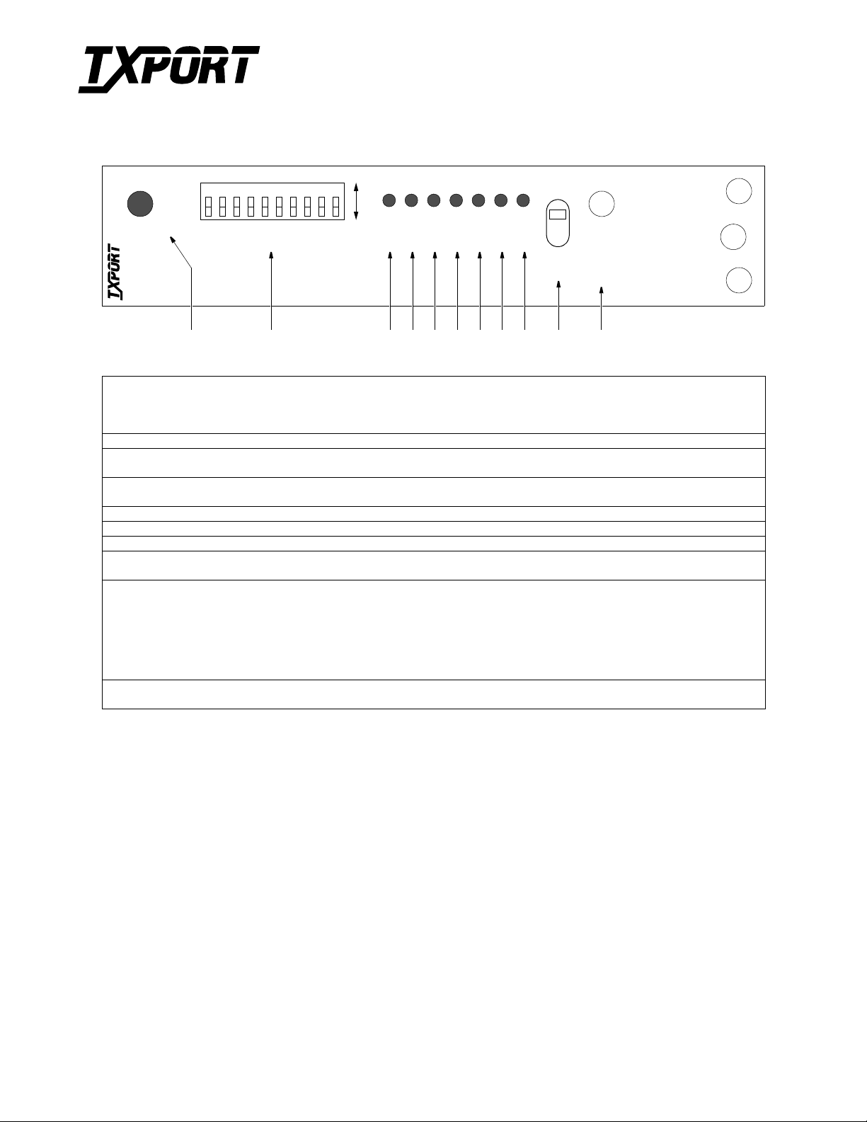
4010 Front Panel
LOC
Part Number 45-00084
Rev 1.01
®
TRANSPORT
IN SERVICE
SW1
DDS
4010
CSU/DSU
1
2 3 4 5 6 7 8 9 10 11
AB
TXD
RXD
RTS
CTS
DCD
232
V.35
FAR
LOOP TEST
Front Panel Description
1 In Service: This three-color IN SERVICE LED indicates the DDS loop receiver’s operating status as follows:
GREEN: Indicates DDS signal at the receiver (either customer dat a or zero suppression).
AMBER: Indicates DDS signal is still present, but received data is idle or out of service.
RED: Indicates an insufficient signal for the DDS receiver to operate properly.
2 Switch SW1: This 10-position LED switch is described on the reverse side.
3 TXD: This green transmit-data LED lights when the data lead is a mark and is off when the data lead is a space.
Therefore, the LED varies from full intensity to off, depending on the relative number of marks and spaces.
4 RXD: This green receive-data LED lights when the data lead is a mark and is off when the data lead is a space.
Therefore, the LED varies from full intensity to off, depending on the relative number of marks and spaces.
5 RTS: This green request-to-send LED lights when circuit CA is in the ON state at the DSU interface.
6 CTS: This green clear-to-send LED lights when circuit CB is in the ON state at the DSU interface.
7 DCD: This green receive-line-signal-detector LED lights when circuit CF is in the ON state at the DSU interface.
8, 9 V.3 5 and 232: The green V . 35 LED is ON when the DTE electrical interface is set to V.35. The green 232 LED is ON when
the interface is set to RS-232. If neither light is on, the configuration switches are set incorrectly.
10 Test Switch: This three-position switch operates as follows:
The LOC position places the unit in a local-loop mode. Data from the DTE is looped back to the DTE. Data from the
network is looped back to the network.
The FAR position initi ates an automated V.54 remote loop and BERT sequence of assigned data channels. The TEST LED is
green if the test is successful (the far-end unit loops and returns the data error free with the V.54 code). If errors are detected, the
TEST LED is red.
The center positi on deactivates the loop codes for normal operation.
11 LOOP TEST: This LED remains amber if there is a local loop or a remote loop. The LED turns red if the V.54 BERT test
fails or green if the V.54 BERT test passes.
Specifications
Network Interface
Line Rate: 2.4, 4.8, 9.6, 19.2, 28, 38.4, 56, and 64 kbps
Line Code: AMI
Line Impedance: balanced 135 Ω
Input Signal: +1 to - 4 0 dB (ALBO)
Output Signal: 3.0 V (±15% ) ba se-peak into 135 ¾,
1.5 V (±15%) at the 9.6 kbps line rate
Line Protection: 1000 V lightning, input and output
Power
Power: -4 8 VDC (± 10%), 50 mA max,
3 watts, 10 BTU max
Connection: Powered throug h chassis
Mechanical
Mounting: 1051 nest mount chassis
Dimensions: 6.8" H, 1.75" W , 10.5" D
Weight: 2 lbs.
Industry Standards
FCC Compliance: Part 15 Subpart B, Class A
FCC Part 68 Reg: FXKUSA-2 2989 -DE -N
NRTL:
CSA Certified:
AT&T TR 62310
AT&T TR 41450
Environmental
Operating Temp: 0° to 50°C (32° to 122°F)
Storage Temp: -20° to 85°C (-4° to 185°F)
Humidity: 95% max (non-condensing)
Page 2
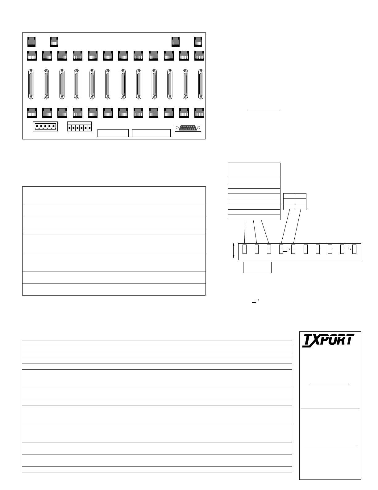
TxPORT 1051-2 Chassis Rear View
Notes:
( B )
NMS
IN
12
11 10 9 8 7 6 5 4 3 2 1
TB1 TB2
( B )
NMS
OUT
T1 DTE
High Speed DTE
T1 NET
TB1 TB2
( A )
NMS
IN
( A )
NMS
OUT
ENET
123456789101112
123456789101112
The RS-232 version of the chassis is shown. The V.35 version is also available.
The 4010 DDS CSU/DSU is only for use in the TxPORT-model 1051 chassis.
Switch SW1 Description
1 - 3 Channel Bit Rate Select: These three positio ns select t he channe l bit rate (refer to
the table on the right). The RTS-to-CTS delays are multiplied by two when SW1-10 is
in the B position.
4 Line Clock: This positi on selec t s ei th er an inte rna l clo ck ing s ou rce or a loo p tim ing
source from the received data.
5 Internal Clock: This position selects either the DSU external clock input or the crystal
oscillator as the clocking source. It is applicable only if SW1-4 is in the B position.
6 V.54 Loop Operation: This position enables or inhibits V.54 loop operation.
7 Data Polarity: This position determines whether data bits are inverted. In the A position,
marks equals pulses. In the B position, spaces equal pulses. Receipt of OOF, OOS, idle, or
loop codes forces the DSU data to all marks (A position) or spaces (B position).
8 Circuit Assurance: On allows the status of CF (rec eive line signal detector) and CA
(request to send) to control the output CB (clear to send). If either CA or CF is Off (A
position), CB is Off. If CA and CF are On (B posit ion ), CB is On.
9 RTS/CTS Control: In the B position, CTS is forced On regardless of the RTS input
status. In the A position, delays are deter mine d by SW1- 10.
10 RTS-to-CTS Delay: In the A position, the RTS-to-CTS delay is as shown in the bit
rate table of the diagra m . In the B position, the de lays shown are multiplied by two.
Standard Equi pment:
A cable is supplied for the NET
connector which puts the DDS si gn al on th e prop er pai rs.
The TxPORT part number is 9-1001-069-1. If this cable
is not used, the DD S output (TX ) is on pins 4 and 5 and
the DDS input ( RX) is on pi ns 1 an d 2 of t h e T1 n et work
connector.
DTE Interface:
The rear of the circuit card has Switch
S1 and Switch S2 which are used to select the type of
DTE interface. Move
select a V.35 interface
both
switches to the V.35 position to
(factory default) or move
both
switches to the 232 position to select an RS-232 in terfa ce.
Factory Defaults:
The A position is the factory default
for Switch SW1 settings. If a particular user configuration requires that a switch be place d in the B position,
then mark this sheet for future reference.
Switch SW1
Rate
123
(kbps)
2.4 B B B 8 ms
4.8 A B B 4 ms
9.6 B A B 2 ms
19.2 A A B 1 ms
28 B B A 0.8 ms
38.4 A B A 0.5 ms
56 B A A 0.4 ms
64 A A A 0.3 ms
A
B
Channel
Bit Rate
The symbol indicates that th e sw itch po inte d to d oes not f unction unless the opposite end of the arrow is in the position shown. For
example, SW1-5 does not function unless SW1-4 is in the B position.
RTS-
to-CTS
Delay
Network (slave)
n/a
BAA
BBExternal
Line Clock
Master
V.54 Loop
Inhibited
65431 7 982
Enabled
V.54 Loop
Internal Clock
RTS-to-CTS Delay
Data Polarity
Circuit Assurance
Normal
Off
On
Inverted
Data Polarity
Circuit Assurance
RTS/CTS Control
RTS/CTS Control
RTS Normal Delay
10
RTS Control On
Normal
2
×
RTS-to-CTS Delay
V.35 and RS-232 Interface
Ckt. V.3 5 RS-232 Signal Name - Function DCE
101 A 1 Frame Ground - This circuit is used to terminate shields. Gnd
102 B 7 Signa l Gro und - This circuit is used as the retu rn reference for unbalanced signals. Gnd
103 P/S 2 / 14 Transmit Data - This input is used for synchronous TD from the DTE. It is transmitted on the DDS side. In
104 R/T 3 / 16 Receive Data - This output is the data decoded from the incoming DDS receive data. Out
105 C 4 Request To Send - This input is a control line from the DTE, indicating data is to be transmitted. When RTS
is ON (space), the data tra nsmitter, the zero suppression circuit ry, and the CTS are ena bled. Wh en RTS is
106 D 5 Clear To Send - This output is a DCE respo nse, i ndica ting that eith er RTS is ON or SW1-9, posit ion B, is
107 E 6 Data Set Ready - This output is ON when t he unit is not in a test mode (other than a V.54 test). Out
109 F 8 Data Carrier Detect - This outp ut is ON when the correct data or zero suppression cod e is being rec eived
113 U/W 24 / 11 External Transmit Clock - This is the synchronous transmit clock input from the DTE. When both SW1- 4 and
114 Y/AA 15 / 12 T ransmit Clock - This output is supplied by the DCE as an external DTE timing source. It is generated from the
115 V/X 17 / 9 Receive Clock - This clock output is the timing for the RD and is always used to time the receive data. This
OFF, the transmitter sends idle code and the CTS is forced OFF.
Out
forcing RTS ON. When SW1-8 is in position B, RTS and RLSD must be ON for CTS to be ON.
Out
and DSR is ON. It is OFF when either DSR is OFF, the DDS receiver has lost sufficient signal to operate
for at least one second, or the receiver has received OOS, OOF, idle, or loop codes for about 20 U.I.
SW1-5 are in the B position, this clock controls the frequency of the DDS transmit clock and clocks circuit 103
(TD). When either SW1-4 or SW1-5 is in the A position, this input has no effect on DDS operation.
Out
internal data clock or the far-end transmit data. Not available if SW1-4 and S1-5 are in the B position.
Out
clock is always derived from the DDS receive data.
Note: When two pins are listed, RS-232 uses the first pin. All pins not specified are open.
TRANSPORT
TxPORT
127 Jetplex Circle
In
Madison, Ala ba m a 35758
Customer Service
800-926-0085, ext. 2227
888-4TxPORT, ext. 2227
Product Technical Support
(8 a.m. to 5 p.m. Central)
888-4TxPORT ,
In
800-285-2755, or
205-772-3770
Emergency After Hours
800-285-2755
E-Mail (Internet Address):
support@txport.com
customer@txport.com
®
 Loading...