

Page 1
TRANSPORT
TRANSPORT
4010
DDS
CSU\DSU
LOOP TEST
INSERVICE
SW1
1 2 3 4 5 6 7 8 9 10
TSD
RXD
RTS
CTS
DCD
V.35
232
LOCFAR
1
2
3
4
5
6
7
8
9
10
11
®
Pins Description
1
2
3
4
5
6
7
8, 9
10
11
PRISM 4010
45-000135
1.0
Configuration Guide (Standalone Version)
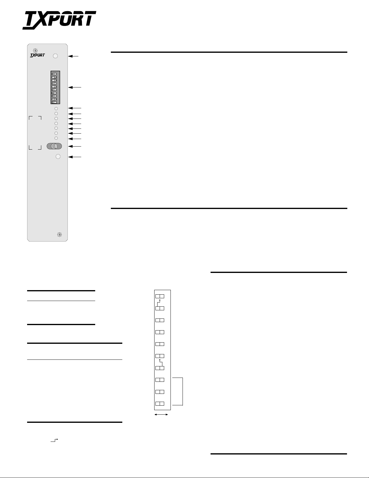
Front Panel Description
In Service - This three-color IN SERVICE LED indicates the DDS loop receiver’s operating status as follows.
Green: Indicates DDS signal at the receiver (either customer data or zero suppression).
Amber: Indicates DDS signal is still present, but received data is idle or out of service.
Red: Indicates an insufficient signal for the DDS receiver to operate properly.
Switch SW1 - This 10- position LED switch is described below.
TXD - This green transmit-data LED lights w hen the data lead is a mark and is off when the data lead is a space.
Therefore, the LED varies from full intensity to off, depending on the relative number of marks and spaces.
RXD - This green re ceive-data LED lights when the da ta lead is a mark and is off when the data lead is a space.
Therefore, the LED varies from full intensity to off, depending on the relative number of marks and spaces.
RTS - This green request-to-send LED lights when circuit CA is in the ON state at the DSU interface.
CTS - This green clear-to-send LED l igh ts when circuit CB is in the ON state at the DSU interface.
DCD - This green receive-line-signal-detector LED lights when circuit CF is in the ON state at the DSU interface.
V.35 and 232 - The green V .35 LED is on when the DTE electrical interface is set to V.35. The green 232 LED is
on when the interface is set to RS- 232. If neither light is on, the configuration switc hes are set incorrectly.
Test Switch - This three- position switch operates as follows.
The LOC position places the unit in a local-loop mode. Data from the DTE is looped back to the DTE. Data from
the network is looped back to the network.
The FAR position initiates an automated V.54 remote loop and BERT sequence of assigned data chann el s . T he
TEST LED is green if the test is successful (th e far-end unit loops and returns the data error free with the V.54
code). If errors are dete ct ed, the TEST LED is red.
The center position dea ct ivates the loop codes for normal operation.
LOOP TEST - This LED remains amber if there is a local loop or a remote loop. The LED turns red if the V.54
BERT test fails or green if the V.54 BERT test passes.
PRISM 4010
Front Panel
Switch SW1
Rate (kbps) SW1-4 SW1-5
Network (slave) A n/a
Master B A
External B B
Rate
SW1-1 SW1-2 SW1-3
(kbps)
RTS-toCTS Delay
2.4 B B B 8 ms
4.8 A B B 4 ms
9.6 B A B 2 ms
19.2 A A B 1 ms
28 B B A 0.8 ms
38.4 A B A 0.5 ms
56 B A A 0.4 ms
64 A A A 0.3 ms
The symbol in dicates that the switch pointed to does not function unless the opposite end of the arrow is in the position shown. For example,
SW1-5 does not function unless SW1-4 is in the B posi ti on.
RTS-to-CTS
Delay Normal
RTS / CTS Control
RTS Normal Delay
Circuit Assurance
Off
Data Polarity
V.54 Loop
Inhibited
A
RTS-to-CTS
10
Delay × 2
RTS/CTS Control
RTS Control On
Circuit Assurance
On
Data Polarity
InvertedNormal
V.54 Loop
65431 7 982
Enabled
Internal Clock
Line Clock
Bit Rate
Channel
B
Pins Description
1 - 3 Channel Bit Rate Sele ct - These three positions select the
channel bit rate (refer to the table on the right). The RTS-toCTS delays are multiplied by two when SW1-10 is in the B
position.
4 Line Clock - This posit ion sele cts either an internal clocking
source or a loop timing source from the received data.
5 Internal Clock - This position selects either the DSU external
clock input or the crystal oscillator as the clocking source. It is
applicable only if SW1-4 is in the B posi ti on.
6 V.54 Loop Operati on - This position enables or inhibits V.54
loop operation.
7 Data Polarity - This position determines whether data bits are
inverted. In the A position, marks equals pulses. In th e B
position, sp aces equal pulses. Receipt of OOF, OO S , i d le, or
loop codes forces the DSU data to all marks (A position) or
spaces (B position).
8 Circuit Assurance - On allows the status of CF (receive line
signal detector) and CA (reque st t o send) to control the output
CB (clear to send). If either CA or CF is Off (A position), CB is
Off. If CA and CF are On (B position), CB is On.
9 RTS/CTS Contro l - In the B position, CTS is forced On
regardless of the RTS input status. In the A po s ition, delays are
determined by SW1-10.
10 RTS-to-CTS Delay - In the A position, the RTS-to-CTS delay is
as shown in the bi t r ate table of the diagram. In the B po sition,
the delays show n are multiplied by two.
Page 2
Rear Panel Pinout
V.35 and RS-232 Interface
NETWORK
Pin
(rear panel)
NETWORK
(9-1001-075-1)
ALARM/POWER
1 Data In (T) Data Out (R1) 48 V Return
2 Data In (R) Data Out (T1) Signal Ground
3 not connected not used -48 VDC
4 Data Out (T1) not used Frame Ground
5 Data Out (R1) not used not applicable
6 not connected not used not applicable
7 Frame Ground Data In (T) not applicable
8 Frame Ground Data In (R) not applicable
1
14
DTE
PORT
25
13
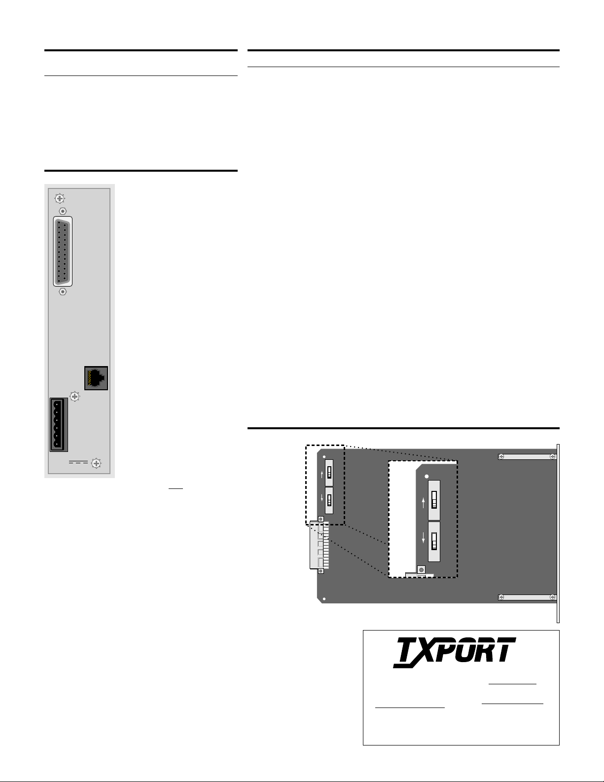
Switch S1 and S2
Access Procedure
1. Open the door.
2. Using both thumbs, gently
spread the plastic front panel
bezel near the LEDs until it
NETWORK
1
8
1
detaches from the fr ont
panel.
3. Remove the screws from the
front panel.
4. Grasp the sides of the front
panel and remove the unit
from the housing.
ALARM/POWER
6
-48 VDC
5. Refer to Figure Side View of
the 4010 to set S1 and S2.
Switch S1 and S2
PRISM 4010
Rear Panel
V.35: Set both switches Up.
RS-232: Set both switches Down.
Ckt. RS-232 Signal Name - Function DCE
101 1 Frame Ground - This circuit is used to terminate sh ie lds. Gnd
102 7 Signal Grou nd - This circuit i s used as the re turn reference f or unbalance d signals. Gnd
103 2 / 14 Transmit Data - This input is used for synchrono us TD from the DTE. It is
In
transmitted on the DDS side.
104 3/16 Receive Data - This output is the data decoded from the incoming DDS
Out
receive data.
105 4 Request T o Send - This input is a control line from the DTE, indicating data
In
is to be transmitted. When RTS is ON (space), the data transmitter, the zero
suppression circuitry, and the CTS are enable d. When RTS is OFF, the
transmitter sends idle code and the CTS is force d O F F.
106 5 Clear T o Send - This output is a DCE response, indicating that either RTS is
Out
ON or SW1-9, position B, is forcing RTS ON. When SW1-8 is in position
B, RTS and RLSD must be ON for CTS to be ON.
107 6 Data Se t Ready - This output is ON whe n the unit is not in a test mode
Out
(other than a V.54 test).
109 8 Data Carrie r Det ec t - Thi s ou tput is ON when the correct data or zero
Out
suppression code is being received and DSR is ON. It is OFF when either
DSR is OFF, the DDS receiver has lost sufficient signal to operate for a t
least one second, or the receiver has received OOS, OOF, idle, or loop
codes for about 20 U.I.
113 24/11 External Transmit Clock - This is the synchronous transmit clock input
In
from the DTE. When both SW1-4 and SW1-5 are in the B position, this
clock controls the frequency of the DDS transmit clock and clocks circuit
103 (TD). When either SW1-4 or SW1-5 is in the A position, this input has
no effect on DDS operation.
114 15/12 Transmit Clock - This output is suppl i ed by the D CE as an ext ernal DTE
Out
timing source. It is generated from the internal data c loc k or the far-end
transmit data. No t availabl e if SW1-4 and S1-5 are in the B posi tion.
115 17/9 Receive Clock - This clock output is the timing for the RD and is always
Out
used to time the receive data. This clock is always derived from the DDS
receive data.
Note: When two pins are li sted, RS-232 only uses the first pin; V.35 uses both. All pins not
specified are open.
S1 S2
V.35 S1, S2 RS232
S1 S2
V.35 S1, S2 RS232
Specifications
Network Interface
Line Rate: 2.4, 4.8, 9.6,19.2, 28,
38.4, 56, and 64 kbps
Line Code: AMI
Line Impeda nce: balanced 135 Ω
Input Signal: +1 to - 40 dB
(ALBO)
Output Sig n a l: 3.0 V (±15%) base-
peak into 135 Ω,
1.5 V (±15%) at the
9.6 kbps line rate
Line Protection: 1000 V lightning,
input and output
Power
Power: -48 VDC (± 10%),
50 mA max,
3 watts,10 BTU max
Connection: Terminal strip
Mechanical
Mounting: Standalone
Dimensions: 6.8" H, 1.75" W,
10.5" D
Weight: 2 lbs
Industry Standards
FCC Compliance:Part 15 Subpart B,
Class A
Part 68 Reg
Industry Canada: CS03
US Safety: UL 1459
Canadian Safety: CSA22.2,No. 225-M90
AT&T TR 62310
AT&T TR 41450
Environmental
Operating Temp: 0° to 50° C
(32° to 122°F)
Storage Temp: -20° to 85°C
(-4 ° t o 185°F)
Humidity: 95% max
(non-condensing)
Side View of the 4010
TRANSPORT
127 Jetplex Circle
Madison, Alabama 35758
Sales and Marketing
800-926-0085
256-772-3770
info@txport.com
®
Returns/RMA
800-926-0085, ext. 2227
Technical Support
800-285-2755
256-772-3770
support@txport.com
 Loading...