

Page 1
TRANSPORT
®
400 DDS DSU/CSU
Configuration Guide
45-00061
3.0
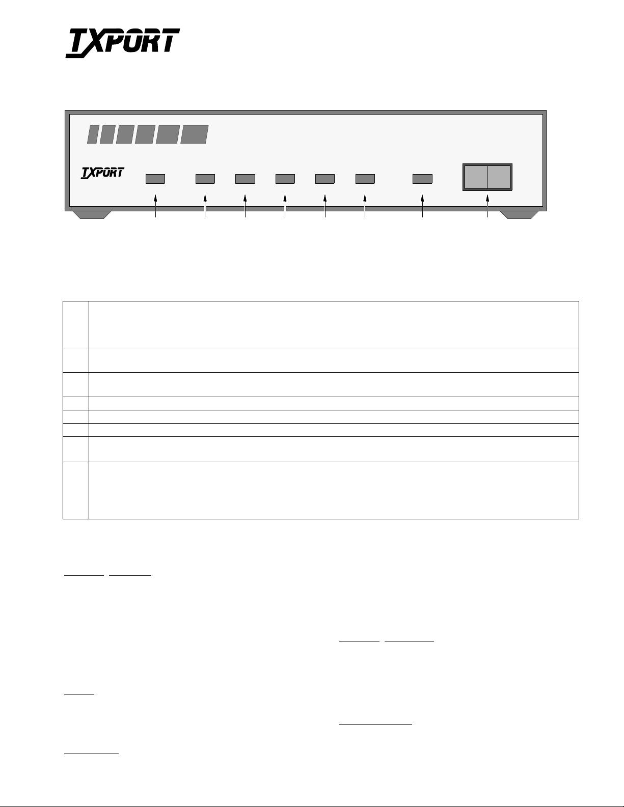
TxPORT 400 Front Panel
PRODUCTIVITY SERIES 400
NORM
RL LL
8
TRANSPORT
DSU/CSU
®
OOS
1
SD RD RTS CTS RLSD
(BA) (BB) (CA) (CB) (CF)
LOOP
TEST
765432
Front Panel Description
1
2
3
4
5
6
7
8
This three color Out Of Service LED indicates the DDS loop receiver’s operating status as follows:
OOS:
Green: Indicates DDS signal at the receiver (either customer data or zero suppression).
Amber: Indicates DDS signal is still present, but received data is idle or out of service.
Red: Indi cates an insufficient signal for the DDS receiver to operate properly.
This green Send Data LED illuminates when the data lead is a mark and is Off when the data lead is a space.
SD:
Therefore, the LED will vary from full intensity to Off depending on the relative number of marks and spaces.
This green Receive Data LED illuminates when the data lead is a mark and is Off when the data lead is a space.
RD:
Therefore, the LED will vary from full intensity to Off depending on the relative number of marks and spaces.
This green Request To Send LEDilluminates when circuit CA is in the On state at the DSU interface.
RTS:
This green Clear To Send LED illuminatets when circuit CB is in the On state at the DSU interface.
CTS:
RLSD:
TEST:
of a test command from the facility. The LED turns red or green at the end of a V .54 test indicating the pass or fail state of the BERT.
Test Switch:
looped back to the DTE. Data from the network is looped back to the network. The RL position initiates an automated V.54 remote
loop and BERT sequence of assigned data channels. The TEST LED will illuminate green if the test is successful (the far end unit
loops and returns the data error free with the V.54 code). If errors are detected, the TEST LED will illuminate red. The NORM
position deactivates the loop codes for normal operation.
This green Receive Line Signal Detector LED illuminates when ci rcuit CF is in the On state at the DSU interface.
This amber LED remains i llumina ted if the u nit is in a t est m ode, eith er b y m anually dep ressing th e loop switch o r b y rec eipt
This 3-position switch is used as follo ws: The LL position places the unit in a loc al loop mode. Data from the DTE is
Network Interface
Line Rate: 2.4, 4.8, 9.6, 19.2, 28, 38.4, 56,
and 64 kbps
Line Code: AMI
Line Impedance: balanced 135 Ω
Input Signal: +1 to -40 dB (ALBO)
Output Signal: 3.0 V (±15%) base-peak into 135 Ω,
1.5 V (±15%) at the 9.6 kbps line rate
Line Protection: 1000 V lightning, input/output
Power
AC Power: 115 VAC (± 10%), 150 mA max,
20 Watts, 73 BTU max.
Connection: 5-foot power cord
Mechanical
Mounting: Desktop or wall
Specifications
Dimensions: Height: 1.75 inches (4.45 cm)
Wide: 6.8 inches (17.27 cm)
Depth: 10.5 inches (26.67 cm)
W e ig ht: 2 pounds (0.91 kg)
Industry Standards
FCC Compliance: Part 15 Subpart B, Class A, Part 68
U.S. Safety: UL 1459
Canadian Safety: CSA C22.2 No. 225-M90
IC: CS03
Environmental
Operating Temp: 0° to 50° C (32° to 122°F)
Storage Temp: -20° to 85° C (-4° to 185°F)
Humidity: 95% max (non-condensing)
Page 2
115 VAC
TRANSPORT
®
V.35
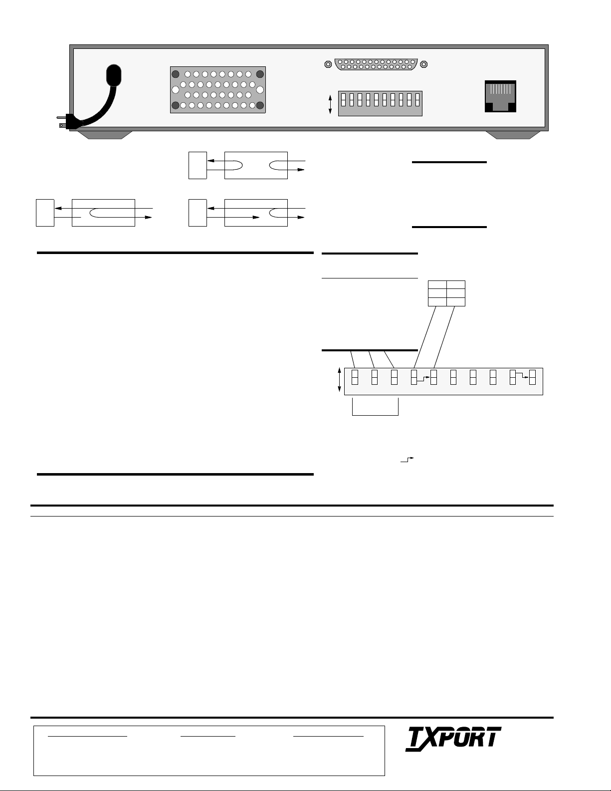
TxPORT 400 Rear Panel
13 1
A
B
RS232
S1
DDS
1425
10765432 81
9
NET
81
Local Loopback
DDS NET Pinout
Remote Channel Loop
(V.54) and Data Set Loop
DTE
Loops
NET
DTE
Channel Lo op (Manda tory Loop)
DTE
NET
NET
1 Data Out R
2 Data O ut T
3-6 Not Used
7 Data In T1
8 Data In R1
Switch S1
1-3
Channel Bitrate Select:
table on the right). The RTS to CTS delays are multiplied by 2 when S1-10 is in the B
position.
4
Line Clock:
source from the received data.
5
Internal Clock:
crystal oscillator as the clocking source. It is applicable only if S1-4 is in the B
position.
6
V.54 Loop Oper at ion :
7
Data Polarity:
position, marks equal pulses. In the B positio n, spaces equal pulses. Receipt of OOF,
OOS, idle, or loop codes forces the DSU data to all ma rk s (A pos ition) or spaces (B
position).
8
Circuit Assurance:
(request to send) to control the output CB (clear to send). If either CA or CF is Off
(position A), CB is Off. If CA and CF are On (position ‘B’), CB is On.
9
RTS/CTS Control:
status. In the A position, delays are dete r mi ne d by S1-10.
10
RTS -> CTS Delay:
rate table of the diagram. In the B position, the delays shown are multiplied by two.
This position selects either an int e rn al clocki ng source or a loop timing
These 3 positions select the channel bit rate (refer to the
This position selects either the DSU exter n a l clock input or the
This position enables or inhibits V.54 loop operation.
This position determines whether data bits are inverted. In the A
On allows the status of CF (receive line signal detector) and CA
In the B position, CTS is forced On regardless of the RTS input
In the A position, the RTS to CTS delay is as shown in the bit
Rate
S1-1 S1-2 S1-3
(kbps)
2.4 B B B 8 ms
4.8 A B B 4 ms
9.6 B A B 2 ms
19.2 A A B 1 ms
28 B B A .8 ms
38.4 A B A .5 ms
56 B A A .4 ms
64 A A A .3 ms
A
B
Channel
Bit Rate
Note: The symbol ‘ ’ indicates that the switch pointed to is not
functional unless the opposite end of the arrow is in the position shown.
For example, S1-5 is not functional unless S1-4 is in the B position.
RTS
to CTS
Delay
Line Clock
n/a
BAA
BB
V.54 Loop
Inhibited
65431 7 982
Enabled
V.54 Loop
Internal Clock
Network (slave)
Master
External
Data Polarity
Circuit Assurance
Normal
Off
On
Inverted
Data Polarity
Circuit Assurance
RTS/CTS Control
RTS/CTS Control
RTS Normal Delay
RTS Control On
RTS - > C TS Delay
10
RTS->CTS Delay
V.35 and RS-232 Interface
Ckt. V.3 5 RS-232
101 A 1 Frame Ground - This circuit is used to terminate shields. Gnd
102 B 7 Signal Ground - This circuit is used as the return reference for unbalanced signa ls. Gnd
103 P /S 2 Transmit Data - This input is used for synchronous TD from the DTE. It is transmitted on the DDS side. In
104 R/T 3 Receive Data - This output is the data decoded from the incoming DDS receive data. Out
105 C 4 Request To Send - This input is a control line from the DTE indi cating data is to be transmitted. When RTS is On (space), the data transmitter,
106 D 5 Clear To Send - This output is a DCE response, indica ting that either RTS is On or S1-8, position B, is forcing RTS ON. When S1- 7 is in
107 E 6 Data Set Ready - This output is On when the unit is no t in a test mode (o the r tha n a V.54 test). Out
109 F 8 Data Carrier Detect - This output is On when the correct data or zero suppression code is being received and DSR is On. It is Off when either
113 U/W 24 External Transmit C loc k - This is the synchronous transmit clock input from the DTE. When both S1-3 and S1-4 are in the B position, this
114 Y/AA 15 Transmit Clock - This output is suppli ed by the DCE as an external DTE timing source. It is generated fro m the internal data clock or the far
115 V/X 1 7 Receive Clock - This clock output is the timing for the RD and is always used to time the receive data. This clock is always derived from the
142 K 2 5 Test Mode - This output is On when the unit is in the Test/Loop mode. Out
the zero suppression circuitry, and the CTS are enabled. When RTS is Off, the transmitter sends idle code and the CTS is forced Off.
position B, RTS and RLSD must be On for CTS to be On.
DSR is Off, the DDS receiver has lost sufficient signal to operate for at least one second, or the receiver has received OOS, OOF, idle, or loop
codes for about 20 U.I.
clock controls the frequency of the DDS transmit clock and clocks circuit 103 (TD). When e ither S1- 3 or S1-4 is in the A po sit ion, this input
has no effect on DDS operation.
end transmit data. Not available when S1-3 and S1-4 are in the B position.
DDS receive data.
Signal Name - Function
(Note: all other pins are open)
DCE
Out
Out
Out
Out
Normal
X 2
In
In
Sales and Marketing
800-285-2755
205-772-3770
info@txport.com
Returns/RMA
800-926-0085, ext. 2282
205-772-3770, ext. 2282
Technical Support
800- 285-2755
205- 772-3770
support@txport.com
127 Jetplex Circle
Madison, AL 35758
 Loading...