

Page 1
©
Panel Scope
VPS10
Technical Doc
10/02/2005
Page 2

A division of Velleman® Components
Legen Heirweg 33
9890 Gavere
BELGIUM Europe
www.vellemaninstruments.com
VPS10 TD1.0
Page 3
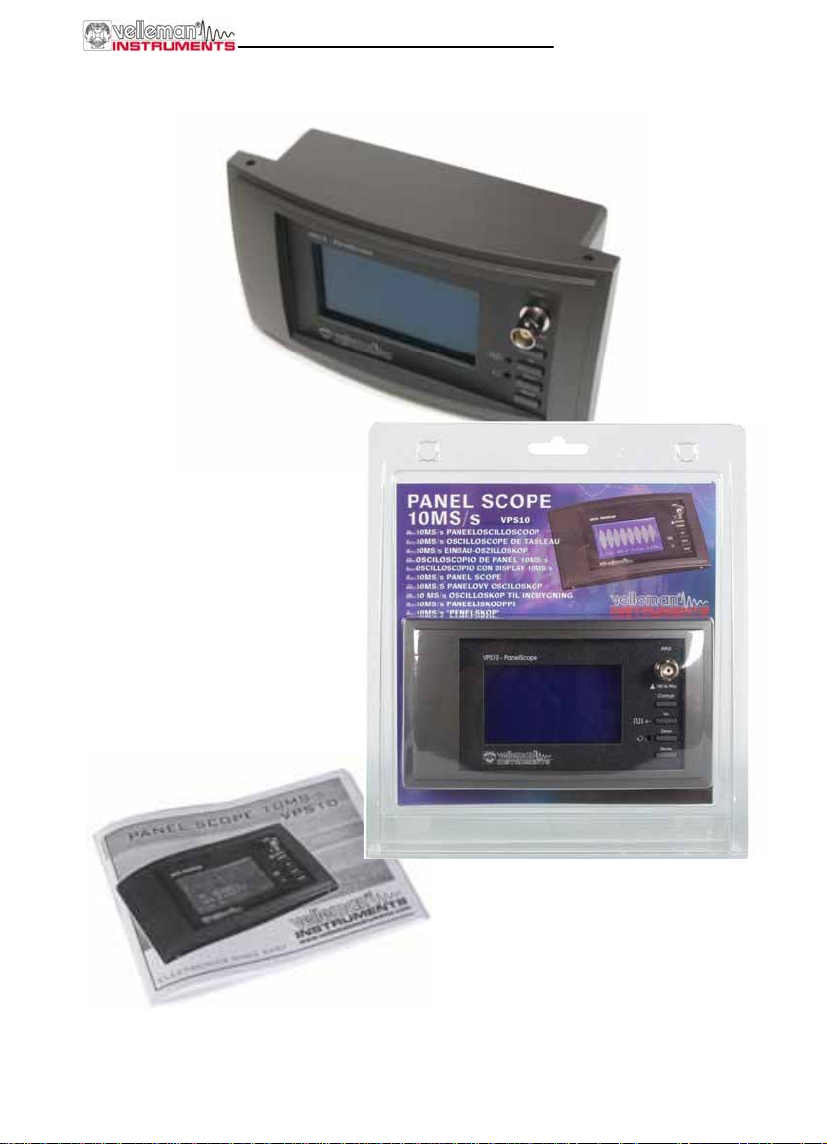
IN THE PACKAGE:
VPS unit
User Manual
UK, NL, D, FR, SP
VPS10 Technical Doc
Page 4
VPS10 Technical Doc
A division of Velleman Components
SAMPLE FOR APPROVAL
Model type :
Description :
Sample number:
Customer :
VPS10
Panel Scope
Remarks / modifications to previous sample:
Includes:
Prepared by: Approved by: Customer acceptance by:
Please return signed copy
DATE : DATE : DATE :
Page 5

VPS10 Technical Doc
Declaration of Conformity
We, Manufacturer
Velleman Components
Legen Heirweg 33
9890 Gavere
Belgium
declare that the product
VPS10 Panel Scope
if used according the instructions included with the unit meet the directives
in accordance with 89/336/EEC-EMC Directive
and
EN 55022 Limits and methods of measurement of radio interference characteristics of informa-
tion technology equipment (CISPR22 limits)
EN 50082-1 Electromagnetic Compatibility - Generic immunity standard
IEC 1010-1 Safety requirements for equipment for measurement, control and laboratory use (*)
(*) if equipment used with safety measurement probe
FCC Part 15 Part B Unintentional radiators
For the manufacturer
Date: 10/02/2005
Signature: _____________________________
Name: Stephan Santens
R&D manager
Page 6
VPS10 Technical Doc
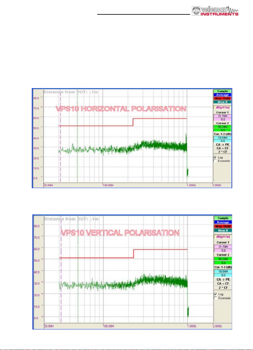
VELLEMAN Instruments
VPS10 1 CH Panel Scope
EN55022 Field strenght
Start frequency: 30MHZ
End frequency: 1GHz
30dB Probe correction attenuation
Page 7

VPS10 Technical Doc
DATE REVISION OVERVIEW
290904F initial release
100205F fix: sampling stops after store default setting
Page 8

VPS10 Technical Doc
VPS10 Panel Scope 10MS/s
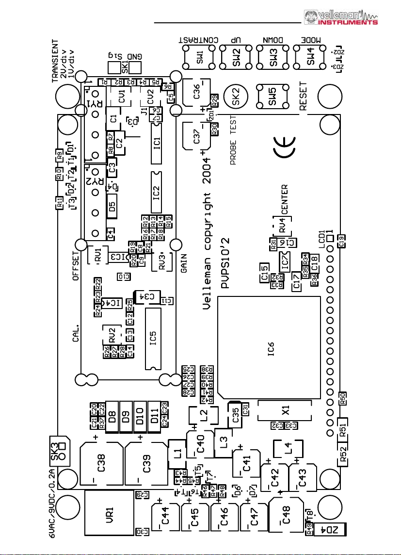
_ASSEMBLY Assembly components for VPS10
_FSVPS10 Polycarbonate front for VPS10
_PANHEADSCREW Screw for PCB fixation
_PV/1 Pan head screw 2,2x6.5mm DIN7981 For BEZEL fixation
_SCREENVPS10 Metal screen for VPS10
_SERIALNR production serial nr (YY-MM- 00000)
_STICK VPS10 Back side info sticker VPS10
BEZEL Universal bezel (top + box)
_CAP_VPS10 Capacitors for VPS10
_100µ/16V smd electrolytic capacitor 16V C36, C37, C40...C47
_100µ/25V smd electro lytic capacitor 25V C48
_100N smd capacitor C4, C10...C14, C19...C31
_10N smd capacitor C5
_1N5/200V smd capacitor 200V C2
_20P/TRIM smd ceramic capacitor trimmer CV1
_22P smd capacitor C32, C33
_27P smd capacitor C8, C9
_330µ/16V smd electrolytic capacitor 16V C38, C39
_330P smd capacitor C6
_4µ7 smd tantalum capacitor C34, C35
_470N smd capacitor C15...C18
_47N/200V smd capacitor 200V C1
_47P smd capacitor C7
_4P7/200V smd capacitor 200V C3
_50P/TRIM smd ceramic capacitor trimmer CV2
_CHOKE_VPS10 Chokes for VPS10
_150µH smd RF choke L1...L4
_CON_VPS10 Connectors for VPS10
_BATCON Male connector on PCB SK3
_BT30300 M3 bolt pan head 3X30mm galvanized SK2
_BTWF2 Wired connector ( idem HPS10) SK3
_CBNC06 BNC female for chassis SK1
_HDR20MAL Male header 20 pole connector 18mm LCD1
_MR3 M3 nut galvanized SK2
_RM3K M3 serrated lock washer (DIN6798AZ) SK2
_DIODE_VPS10 Diodes for VPS10
_BAS45AL smd low-leakage diode D5
_BAT54S smd Schottky barrier double diode D6, D7
_BAV70 SMD high speed double diode D2
_BAV99 SMD high speed double diode D1, D3, D4
_PRLL4001 smd rectifier diode D8...D11
_DISPLAY_VPS10 Display assembly for VPS10
_BT25050 Bolt M2.5x5mm galvanized LCD1
_BUS25FF16 Spacer 16mm - M2.5 LCD1
_HDR20FEM Female header 20 pole connector LCD1
PG12864WRM Blue LCD with backlight for HPS10SE / VPS10 LCD1
_IC_VPS10 IC's for VPS10
_44PLCC LEADLESS CHIP CARRIER 44P IC6
_LM311D SMD Voltage comparator IC4
_LM358D SMD low power dual opamp IC7
_MC14052B SMD analog multiplexer (Motorola) IC2
_MC74HC4052 SMD analog multiplexer/demultiplexer (Motorola) IC1
Page 9

VPS10 Technical Doc
_OPA604AU SMD FET-Input, Audio Operational Amplifier IC3
_TLC5510INSR SMD 8-bit high-speed A/D Converter IC5
VKVPS10 Programmed µcontroller for VPS10 IC6
_PCB_VPS10 Printed circuit board for VPS10
_PVPS10'2 Dual layer pcb for VPS10
_QUARTZ_VPS10 Crystal, oscillator for VPS10
_10MHZ SMD watch crystal X1
_REG_VPS10 Voltage regulators for VPS10
_LM2940S-5.0 smd 5V/1A low dropout voltage regulator VR1
_RELAY_VPS10 Relays for VPS10
_VR05R051AS Reed relais 5VDC / 0.5A / 50mW SIL 1 FORM A RY1...RY3
_RES_VPS10 Resistors for VPS10
_10 (1206) smd resistor R51, R52
_100 (0603) smd resistor R7, R28
_100/1% (0603) smd resistor 1% R5
_100/TRIM smd resistor trimmer (4mm) RV3
_100K (0603) smd resistor R8
_10K (0603) smd resistor R9...R11, R22, R26, R27,
_180/1% (0603) smd resistor 1% R16
_1K (0603) smd resistor R20, R23, R29, R30, R45,
_1M (0603) smd resistor R24
_22K (0603) smd resistor R31
_27/1% (0603) smd resistor 1% R12
_270K (0603) smd resistor R34
_2K2 (0603) smd resistor R37
_2K4/1% (0603) smd resistor 1% R6, R17
_33K (0603) smd resistor R38...R41
_39K/1% (0603) smd resistor 1% R1
_47/1% (0603) smd resistor 1% R14, R15
_47K (0603) smd resistor R32, R33, R35, R36
_47K/1% (0603) smd resistor 1% R4
_47K/TRIM smd resistor trimmer (4mm ) RV1, RV4
_4K7 (0603) smd resistor R42
_4K7/1% (0603) smd resistor 1% R19, R21
_4R7 (0603) smd resistor R25
_500/TRIM smd resistor trimmer (4mm) RV2
_510/1% (0603) smd resistor 1% R3
_560/1% (0603) smd resistor 1% R18
_750/1% (0603) smd resistor 1% R13
_910K/1% (0603) smd resistor 1% R2
_SWITCH_VPS10 Switches for VPS10
_KRS06012 TACTILE SWITCH 6 X 6mm H : 12mm SW1...SW4
_KRS06205 TACTILE SWITCH 6 X 6mm H : 20mm SW5
_TRANS_VPS10 Transistors for VPS10
_PMBT2222A smd npn switching transistor T1...T3, T5...T7
_PMBT2907A smd pnp switching transistor T4, T8
_ZENER_VPS10 Zener diodes for VPS10
_BZD27-C10V smd zener diode 10V/1,3W ZD4
_PLVA2656A Double SMD zener diode 5V6/180mW ZD1...ZD3
Page 10
VPS10 Technical Doc
Page 11
VPS10 Technical Doc
ATT5
ATT4
4K7
R42
+V1
AGND
13
X
Y3A10B
MC14 052B
VDD
16
+V4
X012X114X215X311Y01Y15Y22Y3
IC2
AD IN
27p
C9
AGND
C4
1K
R20
6
47K
RV1
OFFSET
1
OPA60 4UA
IC3
74
+V2
C10
100n
T3
PMBT2222 A
D2
BAV70
+V1
D1
BAV99
VR05R051AS
RY1
+V1
IN1
RY2
AC/DC
10K
R9
PMBT2 222A
DGND
T1
IN2
SK1
5
3
2
AGND
D5
BAS45AL
+V6
IN11
DGND
C3
VR05R051AS
4P7/200V
1K
R29
+V6
IN9
1n5/ 200V
C2
100K
R8
R7
IN12
C1
BNC
39K/ 1%
R1
100
47n/ 200V
AGND
100n
AGND
27p
C8
4K7/ 1%
R19
100
RV3
GAIN
-V2
R21
4K7/ 1%
BAV99
R11
10K
RY3
16
C36
100µ /16V
R2
TRANS 2V/div
ATT1
AGND
10K
R10
T2
13
X
Y3A10B
VDD
MC74 HC4052
X012X114X215X311Y01Y15Y22Y3
IC1
AGND
BAV99
910K /1%
R3
510/ 1%
J1
IN5
IN4
D4
VR05R051AS
IN10
+V4
IN3
CV1
22p
47/1 %
R15
YPOS
ATT2
DGND
PMBT2222 A
R38
AGND
D3
IN6
CV2
50p
C7
47p
C6
330p
27/1 %
R12
180/ 1%
R16
ATT3
33K
R39
33K
9
4
47K/ 1%R4100/ 1%R52K4/ 1%
TRANS 1V/div
C28
33K
R41
100n
33K
R40
100n
9
C27
VEE
VSS
INH
4
47/1 %
R14
750/ 1%
R13
560/ 1%
R18
2K4/ 1%
R17
C26
100n
DGND DGND
100n
C25
VEE
7
VSS
8
DGND
INH
6
AGND
IN8
10n
C5
IN7
-V2
DGND DGND
1K
R30
7
8
DGND
6
R6
AGNDAGND
PLVA2656A
ZD1
AGND
C37
100µ/ 16V
2.0
Eddy De Cocker
4
3
AGND
VPS1 0
Number RevisionSize
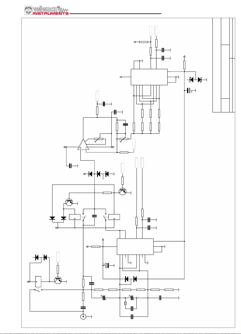
Panel Scope: Anal og sect ion
A4
Title
Date: 16/09/2004 Sheet of
File: C:\Documents and Settings\..\VPS10 Personal Scope Analog Input Section.scDraw n By:
Page 12
VPS10 Technical Doc
YPOS
1
84
IC7A
+V2
3
22K
R31
470n
C16
RV4
47K
CENTER
C15
47K
R32
470n
AGND
47K
R33
7
LM358
IC7B
-V2
2
5
6
AGND
DGND
DATAB US[DB0...DB7 ]
+V1
LM358
DGND
17
18
19
RC1/T1OSI/CCP2
VDD
VDD
RA0/AN03RA1/AN14RA2/AN2/ VREF-5RA3/AN3/ VREF+
AC/DC
SW5
RST
RC2/CCP1
ATT1
VDD
D/I4CS115CS2
16
25
26
20
27
RC5/SDO
RC6/TX/CK
RC4/SDI/SDA
RC3/SCK/SCL
RA4/T0CKI
RA5/SS/LVDIN8RB0/INT036RB441RB2/INT238RB3/CCP239RB1/INT137RB542RB643RB7
6
7
ATT2
ATT3
ATT4
ATT5
RESET
KRS0 611
1K
R23
CONTRAST
LCD1
DB07DB18DB29DB310DB411DB512DB613DB7
E
6
DB0
29
RD0/PSP021RD1/PSP122RD2/PSP223RD3/PSP324RD4/PSP430RD5/PSP531RD6/PSP632RD7/PSP7
RC7/RX/DT
DGND
C18
270K
R34
C17
47K
R35
PWM
47K
R36
X1
+V1
3
470n
2
+V1
100n
C19
1K
R50
470n
DGND
15
16
22p
C33
10Mc
RC0/T1OSO/T1CKI
OSC2 /CLKOUT /RA6
35
12
OSC1 /CLKIN
MCLR/VPP
2
14
C32
22p
DGND DGND
DGNDDG ND
C31
100n
4µ7
C35
+V1
GND
20
VEE
14
DB6
DB7
33
44
VSS
R/W
5
10
9
RE0/RD/AN5
NC1NC17NC28NC
DGND
Up
18
-V1
1
DGND
LCD-P G1286 4
AD OE
AD CLK
11
RE2/CS/AN7
RE1/WR/AN6
VSS
34
VSS
13
DGND
40
DGND
PLVA2656 A
ZD3
PLVA2656A
SW4
SW3
SW2
Mode
Down
A19K
DB1
DB2
DB3
DB4
DB5
IC6
PIC18LF452/L(44)
ZD2
SW1
2.0
4
Eddy De Cocker
4
VPS1 0
Number Revisi onSize
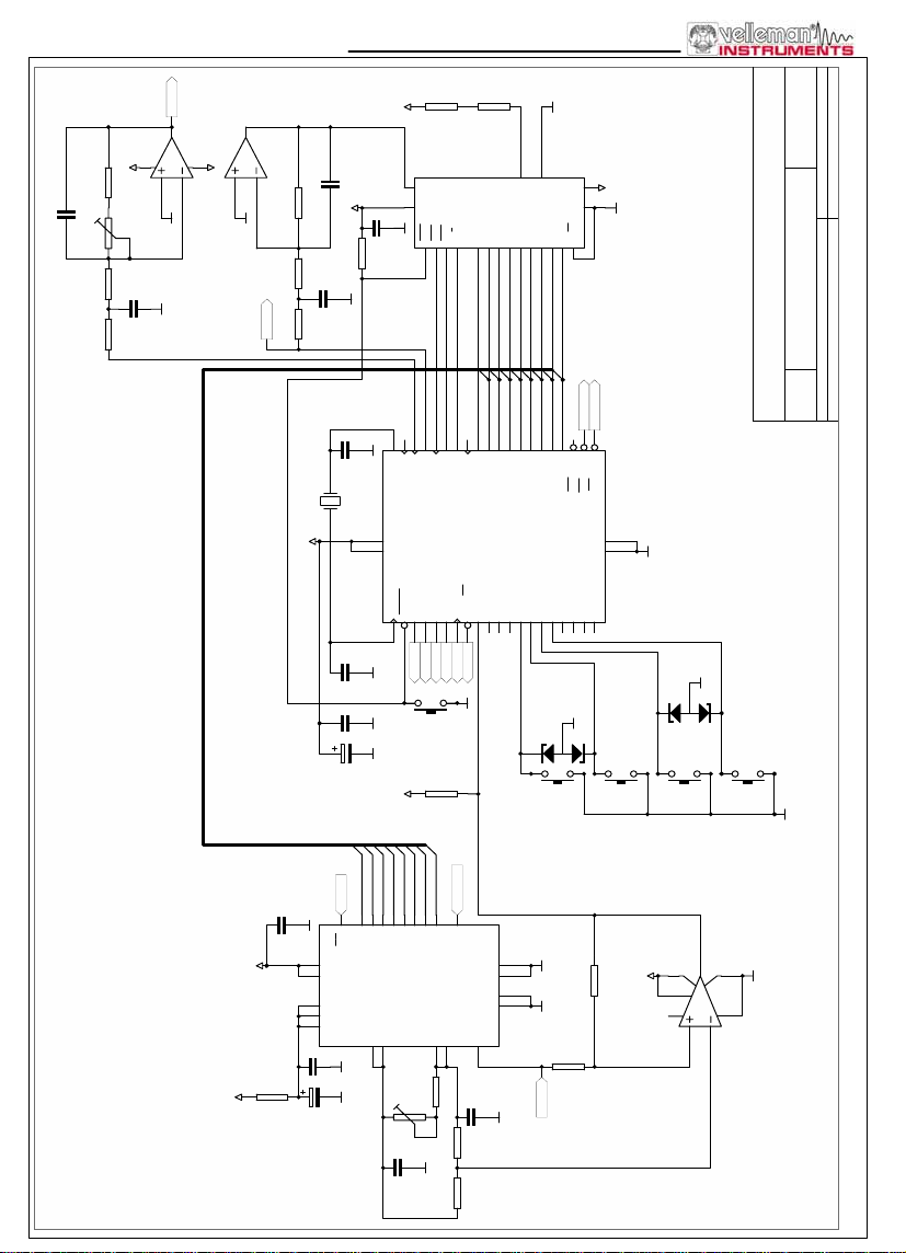
Panel Scope: Digit al Sect ion
A4
Titl e
Da t e : 16/09/2004 Shee t of
File: C:\Documents and Settings\..\VPS10 Personal Scope Digital Section.schDraw n By:
Contrast
DGND
10
R51
10
R52
DB0
DB1
DB2
DB3
DB4
DB5
DB6
DB7
AD OE
1
100n
C11
DGND
OE
DB03DB14DB25DB36DB47DB58DB69DB7
VDDD
13
+V1
4.7
R25
+V6
VDDD
11
VDDA
18
VDDA
15
VDDA
14
C34
REFTS16REFT
C12
17
100n
AGND AGND
4µ7
AD CL K
12
10
CLKIN
DGND
24
DGND
2
IC5
TLC5510INS
CALIBRATION
500
RV2
100n
C13
AGND
21
AGND
20
AN IN
REFB23REFBS
19
22
C14
100
R28
100n
AGND
10K
R27
AGND
10K
R26
1M
R24
AGND DG ND
R22
10K
AD IN
84
+V1
6
5
2
7
DGND
LM311
IC4
1
3
Page 13
VPS10 Technical Doc
+V1
+V6
+V2
-V2
-V1
2.0
Eddy De Cocker
C42
150µ
L4
100µ/16V
C43
100µ/16V
GND
4
2
C44
100µ/16V
AGND
150µ
L1
C40
100µ/16V
3
100n
C29
OUT
GND
4
GND
2
IN
LM2940S-5.0
VR1
C30
1
100n
+V7
L2
0
JP2
L3
150µ
GND AGNDDGND
0
JP1
T8
PMBT2907A
C46
C41
150µ
100µ/16V
AGND
T4
10K
R44
10K
R43
C38
330µ/16V
C39
330µ/16V
C45
PMBT2907A
1K
R45
PMBT2222A
GND GND
ZD4
1K
R49
100µ/16V
100µ/16V
T5
PMBT222 2A
BZD27-C10V
C48
D7
100µ/25V
BAT54S
GND GND GND AGND
C47
D6
100µ/ 16V
BAT54S
GND
T6
PMBT2222A
GND
GND
1K
R46
T7
GND
10K
R48
10K
R47
PWM
GND
VPS10
Number RevisionSize
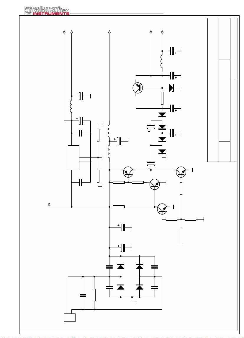
Panel Scope: Power Supply Section
A4
Titl e
Date: 1 6/09/2004 She et of
File: C:\Documents an d Settings\. . \VPS10 Personal Scope Power Supply Section.s chDrawn By:
100n
100n
C24
D10
C20
100n
100n
C21
2K2
R37
-
+
SK3
6VAC or 9VDC/200mA
D8
D11
PRLL4001
D9
PRLL4001
C23
PRLL4001
100n
C22
PRLL4001
GND
Page 14
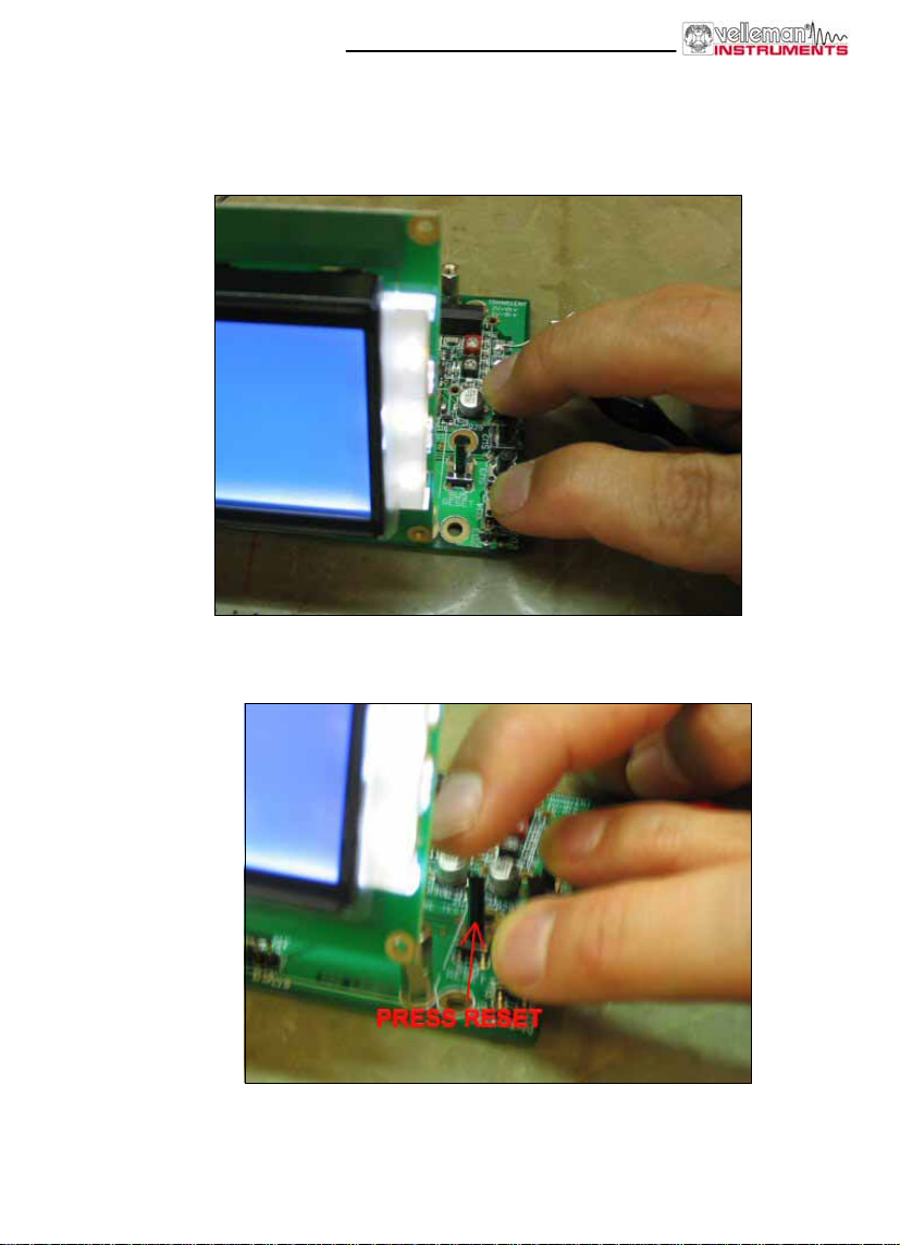
VPS10 Technical Doc
TO START DIAGNOSTIC:
PRESS “MODE” + “CONTRAST” KEYS:
2--PRESS “RESET” AND RELEASE
3 - RELEASE “MODE” + “CONTRAST” BUTTONS
Page 15
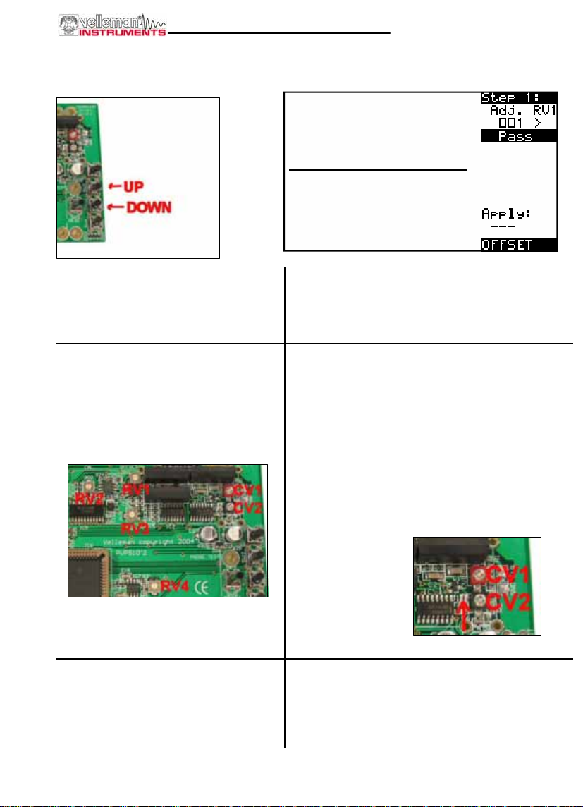
NOW SCOPE IS IN DIAGNOSTIC MODE
Connect signal box to scope input
Set trimpotentiometers RV1… RV4 In center.
1- Offset adjust :
If necessary adjust RV4 to set line in center of
screen
2– 3 Transient adjust:
VPS10 Technical Doc
Adjust offset RV1 until line is stable and display indicates
PASS
Press UP button (display indicates transL)
Connect Transient Test signal (probe test)
If necessary adjust RV3 to get signal in screen
4- DC input selection test: Press UP button (display indicates ac-dc)
Connect
* Adjust contrast for suitable level
Adjust CV1 untill display indicates PASS
Press UP button (display indicates TRANS-H)
Adjust CV2 untill display indicates PASS
REM: if CV2 range is not sufficient, make next solder
BRIDGE connection:
Normal open
Wait until display indicates PASS
Page 16

VPS10 Technical Doc
5 - 6 Input amplifier calibration Press UP button (display indicates call.)
Apply 100mV / 1KHz sine
Apply 100mV / 1KHz sine Press UP button (display indicates gain)
7– 10 Input selector test
Apply 100mV / 1KHz sine
Apply 1V / 1KHz sine
11- Center adjust
Short circuit input
Adjust RV2 (CAL) until display indicates PASS
Adjust RV3 (GAIN) until display indicates PASS
Press UP button: 0.2V/div test
Check PASS
Press UP button: 0.4V/div test
Check PASS
Press UP button: 1V/div test
Check PASS
Press UP button: 2V/div test
Check PASS
Press UP button (display indicates center)
Adjust RV4 (CENTER) until display indicates PASS
12– End
Page 17

VPS10 Technical Doc
SAMPLE RATES
Timebase Sampling interval Samplerate Sample Method
0.2µs/div 0.1µs 10MS/s 4 x oversampling + Sinx/x interpolation
0.5µs/div 0.1µs 10MS/s 4 x oversampling + lin. interpolation
1µs/div 0.1µs 10MS/s 4 x oversampling (2.5 real time)
2µs/div 0.2µs 5MS/s 2 x oversampling (2.5 real time)
5µs/div 0.5µs 2MS/s Real time sampling
10µs/div 1µs 1MS/s Real time sampling
20µs/div 2µs 500kS/s Real time sampling
50µs/div 5µs 200kS/s Real time sampling
0.1ms/div 0.01ms 100kS/s Real time sampling
0.2ms/div 0.02ms 50kS/s Real time sampling
0.5ms/div 0.05ms 20kS/s Real time sampling
1ms/div 0.1ms 10kS/s Real time sampling
2ms/div 0.2ms 5kS/s Real time sampling
5ms/div 0.5ms 2kS/s Real time sampling
10ms/div 1ms 1kS/s Real time sampling
20ms/div 2ms 500S/s Real time sampling
50ms/div 5ms 200S/s Real time sampling
0.1s/div 0.01s 100S/s Real time sampling
0.2s/div 0.02s 50S/s Real time sampling
0.5s/div 0.05s 20S/s Real time sampling
1s/div 0.10s 10S/s Real time sampling
2s/div 0.20s 5S/s Real time sampling
5s/div 0.5s 2S/s Real time sampling
10s/div 1s 1S/s Real time sampling
20s/div 2s 0.5S/s Real time sampling
30s/div 3s 0.333S/s Real time sampling
1min/div 6s 0.166S/s Real time sampling
2min/div 12s 0.0833S/s Real time sampling
5min/div 30s 0.03333S/s Real time sampling
0.25h/div 90s 0.01111S/s Real time sampling
0.5h/div 3min 0.00555S/s Real time sampling
1h/div 6min 0.00277S/s Real time sampling
Page 18

VPS10 Technical Doc
Supply voltage 6Vac or 9VDC/ min 200mA (unregulated) 12VDC possible (see user manual)
Operating temperature 0 to 50°C (32 to 122°F)
Input sensitivity range in 12 steps 5mV to 20V/division at X1- 50mV to 200V/div at X10
Probe calibration output Approx. 2KHz / 5Vpp
Peak to peak AC range (sinewave reference) 0.1mV to 160V (1mV to 1000V with x10 probe) 2% accuracy
Timebase range in 32 steps 0.2µs to 1hour / division
LCD Graphics 64 x 128 pixels / reverse / white backlight
Signal storage 256 samples, max. 125 samples visible (256 using X shift)
dBm measurement (0dBm= 0.775V in 600ohm)
dBV measurements (0dBV= 1V)
True-rms measurement From 0.1mV to 80V (up to 400Vrms with X10 probe) 2.5% accuracy
Trigger modes Run, Normal, Roll mode for 1s/div and slower timebase
SPECIFICATIONS
Maximum sample rate 10MS/s for repetitive signals (2MS/s for single shot events)
Maximum input amplifier bandwidth 2MHz ( -3dB at 50mV, 1V & 20V /div x1 setting)
Input impedance 1Mohm // 20pF (standard oscilloscope probe)
Maximum input voltage 100Vpeak (AC + DC), 200Vpeak-peak (AC only)
Input coupling DC, AC and GND (GND for auto zero reference)
Vertical resolution
From -73dB tot +40dB (up to 60dB with X 1 0 pr o be) + 0.5dB accuracy
From -75dB tot +38dB (up to 58dB with X 1 0 pr o be) + 0.5dB accuracy
8 bit + 1bit linearity
Page 19
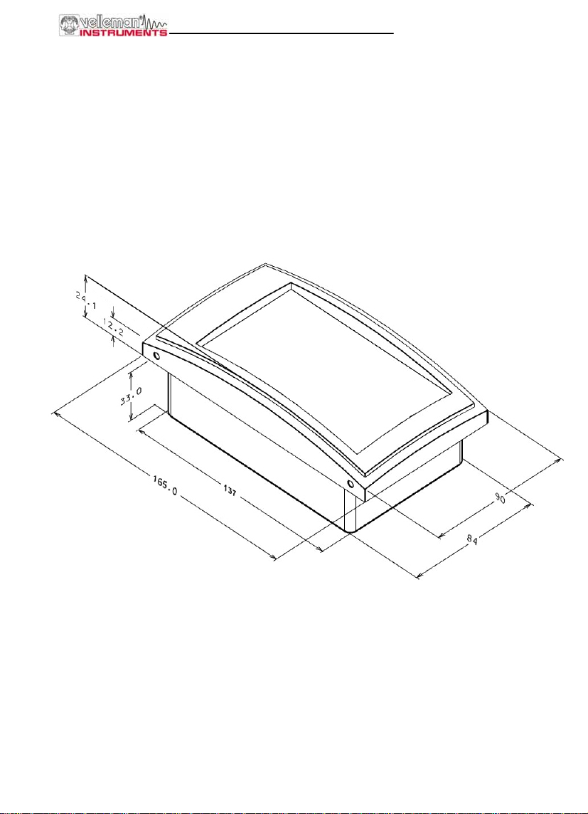
DIMENSIONS
VPS10 Technical Doc
Page 20

A division of Velleman® Components
Legen Heirweg 33
9890 Gavere
BELGIUM Europe
www.vellemaninstruments.com
VPS10 TD1.0
 Loading...