

Buffer
ESD Diodes
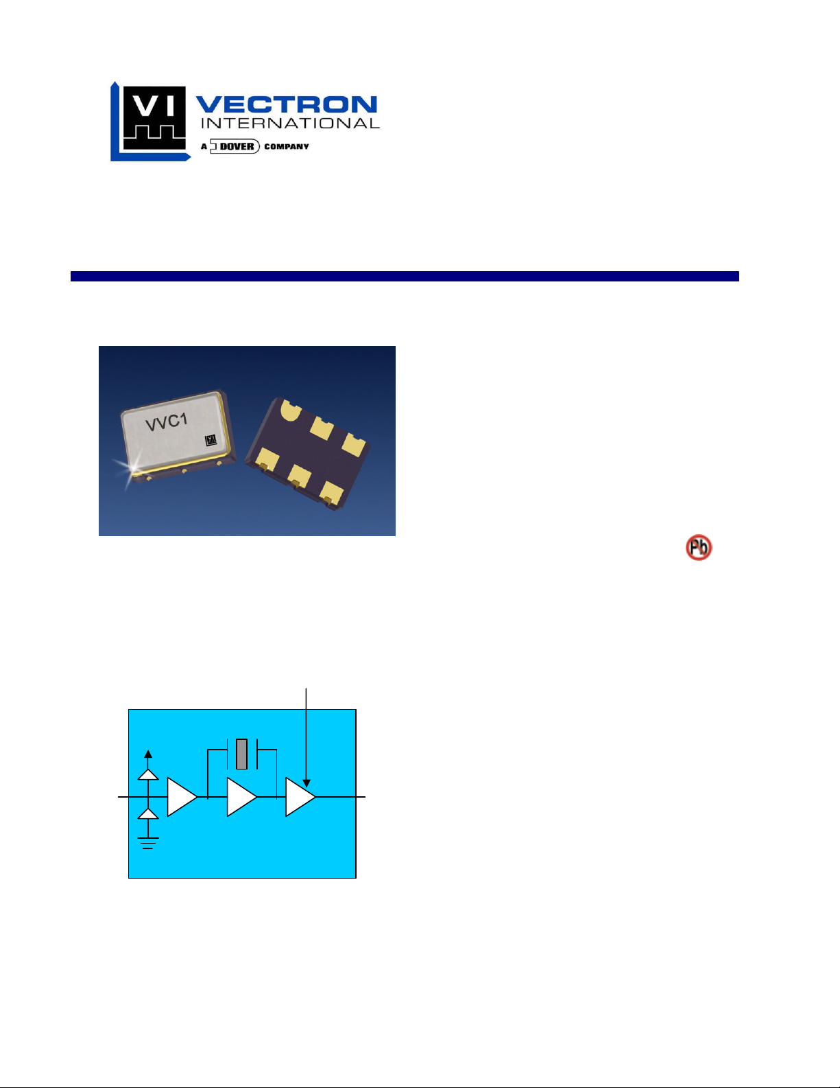
The VVC1 Voltage Controlled Crystal Oscillator
Vc
Input
Output
Buffer /
Tri-state
VVC1/VVC2
Voltage Controlled Crystal Oscillator
Features
• VCXO with a CMOS output
• Small 5.0 X 7.0 X 1. 8 mm package
• Output frequencies to 66 MHz
• 5.0 or 3.3 V operation
• Low Jitter < 6 pS rms, fo>12MHz
• Tri-State Output for test and board debug
• 0/70 or –40/85 °C operating temperature
• Hermetically sealed ceramic SMD package
• Product is compliant to RoHS directive
and fully compatible with lead free assembly
Applications
• SONET/SDH/DWDM
• Ethernet, Gigabit Ethernet
• xDSL/PCMCIA cards
• Digital Video
• Broadband Access
Description
fO
Vectron’s VVC1 Voltage Controlled Crystal
Oscillator (VCXO) is a quartz stabilized square
wave generator with a CMOS output and is tested
at CMOS and TTL (5.0 volt operation) logic levels.
The VVC1 uses fundamental crystals resulting in
low jitter performance and a monolithic IC which
improves reliability and reduces cost.
Vectron International 267 Lowell Road, Hudson NH 03051 Tel: 1-88-VECTRON-1 e-mail: vectron@vectron.com
VVC1 Voltage Controlled Crystal Oscillator
tFt
-
4
3
256
1
1.8k
Performance Characteristics
Table 1. Electrical Performance
Parameter Symbol
Frequency fO 1.544 65.536 MHz
Supply Voltage 1 (+ 5.0 V)
(+3.3 V)
Supply Current (+5.0 V)
(+3.3 V)
Output Logic Levels
Output Logic High2
Output Logic Low2
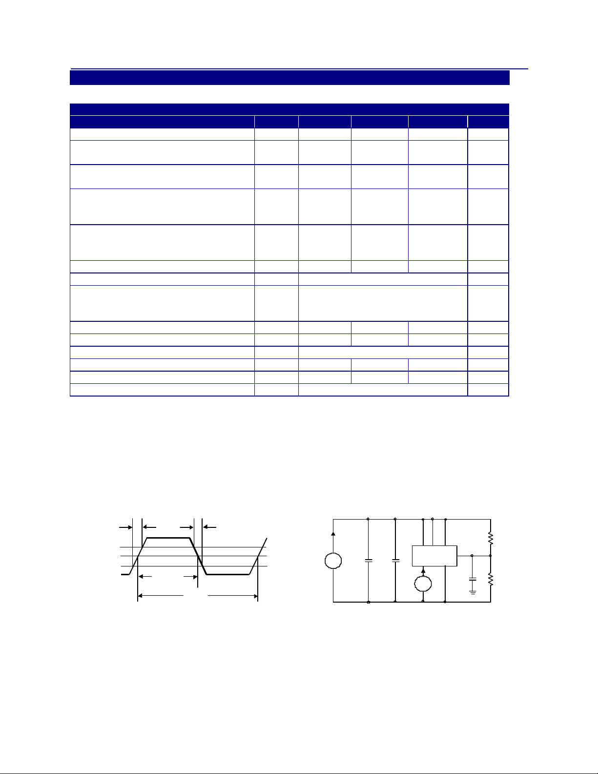
Transition Times
Rise Time2
Fall Time2
V
DD
I
DD
VOH
VOL
tR
tF
Symmetry or Duty Cycle3 SYM 45 50 55 %
Operating temperature (ordering option) 0/70 or –40/85 °C
Total Pull Range (ordering option)
±50, ±100 or ±150
Or
Absolute Pull Range
Test Conditions for APR (+5V option) VC 0.5 4.5 V
Test Conditions for APR (+3.3V option) VC 0.3 3.0 V
Gain Transfer (See Figure 3) Positive ppm/V
Control Voltage Leakage Current I
±1 uA
VCXO
Control Voltage Bandwidth (-3dB) BW 10 kHz
Package Size 5.0 x 7.0 x 1. 8 mm
1. A 0.01uF and a 0.1uF capacitor should be located as close to the supply as possible (to ground) is recommended.
2. Figure 1 defines these parameters. Figure 2 illustrates the equivalent five gate TTL load and operating conditions under which
these parameters are tested and specified.
3. Symmetry is defined as (ON TIME/PERIOD with Vs= 1.4 V for TTL and Vs=2.5 V for CMOS, 5 volt operation, and Vs=1.65V
for 3.3 Volt operation.
Min Typical Maximum Units
4.750
3.135
5.0
3.3
5.250
3.465
55
40
0.9*VDD
0.1VDD
5
5
±50, ±80 or ±100
V
mA
V
V
ns
ns
ppm
R
%
80
Vs
20%
On Time
Period
I
DD
+
µ
.1
-
F .01µF
I
C
+
V
C
V
DD
650Ω
15pF
Figure 1. Output Waveform Figure 2. Typical Output Test Conditions (25±5°C)
Vectron International 267 Lowell Rd, Hudson NH 03051 Tel: 1-88-VECTRON-1 e-mail: vectron@vectron.com

VVC1 Voltage Controlled Crystal Oscillator
Outline Diagram, Pad Layout and Pin Out
Inch/[mm}
Pin # Symbol Function
1 VC Control Voltage
2 NC or Tri-state No Connect or Tri-state
3 GND Ground
4 fO Output Frequency
5 Tri-state or NC Logic low disables output
Logic high or no connection enables output waveform
6 VDD Supply Voltage
Tape and Reel
J
F
CD
A
E
G
B
I
L
KH
Tape and Reel Dimensions (mm)
Tape Dimensions Reel Dimensions # Per
Product A B C D E F G H I J K L Reel
VVC1
12 5.5 1.5 4 8 1.78 20.6 13 55 6 12.4 178
Vectron International 267 Lowell Rd, Hudson NH 03051 Tel: 1-88-VECTRON-1 e-mail: vectron@vectron.com
500

VVC1 Voltage Controlled Crystal Oscillator
Frequency Pull (ppm)
Absolute Maximum Ratings
Stresses in excess of the absolute maximum ratings can permanently damage the device. Functional
operation is not implied at these or any other conditions in excess of conditions represented in the
operational sections of this data sheet. Exposure to absolute maximum ratings for extended periods may
adversely affect device reliability.
Table 2. Absolute Maximum Ratings
Parameter Symbol Ratings Unit
Power Supply VDD 6 Vdc
Storage Temperature Tstorage -55/125 °C
Voltage Control Range VC Gnd to VDD V
200.0
150.0
100.0
50.0
0.0
-50.0
-100.0
-150.0
-200.0
0.30 0.60 0.90 1.20 1.50 1.80 2.10 2.40 2.70 3.00
Control Voltage (volts)
Figure 3. Typical Frequency Pull versus Control Voltage, 35.328MHz Output, 3.3 Volt Supply
Vectron International 267 Lowell Rd, Hudson NH 03051 Tel: 1-88-VECTRON-1 e-mail: vectron@vectron.com

VVC1 Voltage Controlled Crystal Oscillator
Reliability
The VVC1 is capable of meeting the following qualification tests.
Table 3. Environnemental Compliance
Parameter Conditions
Mechanical Shock MIL-STD-883 Method 2002
Mechanical Vibration MIL-STD-883 Method 2007
Solderability MIL-STD-883 Method 2003
Gross and Fine Leak MIL-STD-883 Method 1014
Resistance to Solvents MIL-STD-883 Method 2016
Handling Precautions
Although ESD protection circuitry has been designed into the the VVC1, proper precautions should be taken
when handling and mounting. VI employs a Human Body Model and a Charged-Device Model (CDM) for
ESD susceptibility testing and design protection evaluation. ESD thresholds are dependent on the circuit
parameters used to define the model. Although no industry wide standard has been adopted for the CDM, a
standard HBM of resistance = 1.5kohms and capacitance = 100pF is widely used and therefore can be
used for comparison purposes.
Table 4. ESD Ratings
Model Minimum Conditions
Human Body Model 1500 MIL-STD-883 Method 3115
Charged Device Model 1000 JESD 22-C101
Suggested IR profile
Devices are built using lead free epoxy and can also be subjected to standard lead free IR reflow conditions.
Vectron International 267 Lowell Rd, Hudson NH 03051 Tel: 1-88-VECTRON-1 e-mail: vectron@vectron.com

VVC1 Voltage Controlled Crystal Oscillator
)
Standard Frequencies (MHz)
1.544 2.048 4.096 8.192 10.000
12.000 12.288 12.352 13.000 14.318
15.440 16.000 16.384 18.432 19.440
20.000 20.480 24.576 24.704 27.000
30.000 32.000 32.768 34.368 35.328
38.880 40.000 40.960 44.736 51.840
52.000 62.208 65.536
Other frequencies may be available upon request. Standard frequencies are frequencies which the crystal has been designed
and does not imply a stock position.
Ordering Information
VVC1-BGE – xxMxxx
Product Family Frequency
VC=VCXO example: 44M736= 44.736MHz
Package Temperature Range/Stability(for TPR)
5x7x2 B: 0/70 C, ±50 ppm
TriState D: -40/85 C, ±50 ppm
1=Pin 5 E: 0/70 C, ±25 ppm
2=Pin 2 F: -40/85C, ±25 ppm
Power Supply, Linearity Absolute Pull Range
A: 5.0V , 20% Linearit y G: ±50 ppm APR
B: 3.3V, 20% Linearity N: ±80 ppm APR
C: 5.0V, 10% Linearity H: ±100 ppm APR
F: 3.3V, 10% Linearity or Total Pull Range
1: ±50 ppm
2: ±100 ppm
3: ±150 ppm
NOTE: Not all combinations of options are available. Higher frequencies have less pull capability, especially at +3.3 volts
supply, and higher pull can result in 20% linearity instead of 10%. Consult factory or your local sales representative with
application requirements.
www.vectron.com
Vectron International reserves the right to make changes to the product(s) and/or information contained herein without notice. No liability is assumed
as a result of their use or application. No rights under any patent accompany the sale of any such product(s) or information. VVC1 (June 26 2005
USA: Vectron International • 267 Lowell Road, Hudson, NH 03051
• Tel: 1-88-VECTRON-1 • Fax: 1-888-FAX-VECTRON
EUROPE: VI Telefilter · Potsdamer Straße 18, 14513 Teltow, Germany
Tel: 49 (0) 3328 4784 17 • Fax: 49 (0) 3328 4784 30
ASIA: Vectron Asia Pacific Sales 1F~2F. No.8 Workshop No.308 Fenju Rd., WaiGaoQiao
Free Trade Zone, Pudong New Area Shanghai, China 200131
•Tel: 8621 50480777 • Fax: 8621 50481881
For Additional Information, Please Contact:
Vectron International 267 Lowell Rd, Hudson NH 03051 Tel: 1-88-VECTRON-1 e-mail: vectron@vectron.com
 Loading...