

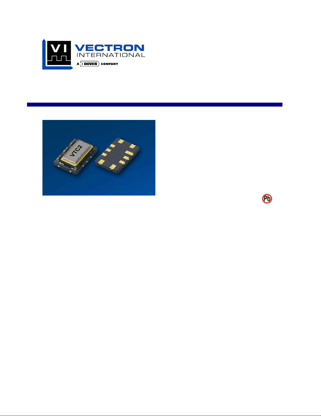
VTC2 series
Voltage Controlled Temperature Compensated Crystal Oscillator
The VTC2, VCTXCO
Features
• CMOS Square Wave Output
• Enable Disable Feature
• Output Frequencies to 30 MHz
• Fundamental Crystal Design
• Optional VCXO function available
• Gold over nickel contact pads
• Hermetically Sealed Ceramic SMD package
• Product is compliant to RoHS directive
and fully compatible with lead free assembly
Applications
• FPGA’s
• A/D’s
• DSL Head End
• Wireless Communications
• Base Stations
• Point to point radios
• Broadband Access
• Test Equipment
Description
Vectron’s VTC2 Temperature Compensated
Crystal Oscillator (TCXO) is a quartz stabilized,
CMOS squarewave , temperature compensated
oscillator, operating off either 2.8, 3.0, 3.3 or 5.0
volt supply.
Vectron International 267 Lowell Road, Hudson NH 03051 Tel: 1-88-VECTRON-1 e-mail: vectron@vectron.com
VTC2 Data sheet
Performance Characteristics
Table 1. Electrical Performance
Parameter Symbol
Min Typical Maximum Units
Frequency fO 10.000 30.000 MHz
Supply Voltage 3.3V ±10% or +5V ±5% VDC
Maximum Supply Voltage 6 VDC
Supply Current , +3.3V IDD 10.0 mA
Output Level
Logic High
Logic Low
Drive High
Drive Low
2
VOH
V
OL
IOH
IOL
0.9*V
4
DD
0.1*V
-4
DD
V
V
mA
mA
Output Load 15pf
Duty Cycle, @ 50% 45/55 %
Control Voltage Impedance ZVc 100 Kohm
Control Voltage to reach pull 0.5 2.5 V
Pull Range
TPR ±5, ±8 ppm
Ordering option, see last page
Temperature Stability
±0.5 to ±5.0 ppm
Ordering option, see last page.
Initial Accuracy, “No Adjust” option ±1.0 ppm
Power Supply Stability ±0.3 ppm
Load Stability ±0.2 ppm
Aging ±1.0 ppm/year
Enable/Disable3
Output Active
Output Disabled
Operating temperature
0.8*VDD
V
0.2*VDD
0/55, -10/60, -20/70, -30/80, -40/85 °C
Ordering option, see last page
Phase Noise, 12.800MHz
10 Hz offset
100 Hz offset
1 kHz offset
10 kHz offset
100 kHz offset
-93
-123
-147
-155
-158
dBc/Hz
Start-up time 2 ms
1. A 0.01uF and a 0.1uF capacitor should be located as close to the supply as possible (to ground) is recommended.
2. Output is DC coupled.
3. Output is active if E/D is open.
Vectron International 267 Lowell Rd, Hudson NH 03051 Tel: 1-88-VECTRON-1 e-mail: vectron@vectron.com
VTC2 Data sheet
VCXO Functional Description
VCXO Feature : The VTC2 can be ordered with a VCXO function for applications were it will be used in a
PLL, or the output frequency needs fine tune adjustments. This is high impedance, 1 Mohm, input and can
be driven with an op-amp or terminated with adjustable resistors etc. Pin 1 should not be left floating on
the VCXO optional devices.
“No Adjust” Feature : In applications were the VTC2 will be not be used in a PLL, or the output frequency
does not fine tune adjustments, the best device to use would be a VTC2-x0xxx. By using the “no adjust”
option, the circuit is simplified as Vc does not need to adjusted or set to a predetermined voltage and pin 1
should be grounded or left open (but not set to a voltage such as the supply).
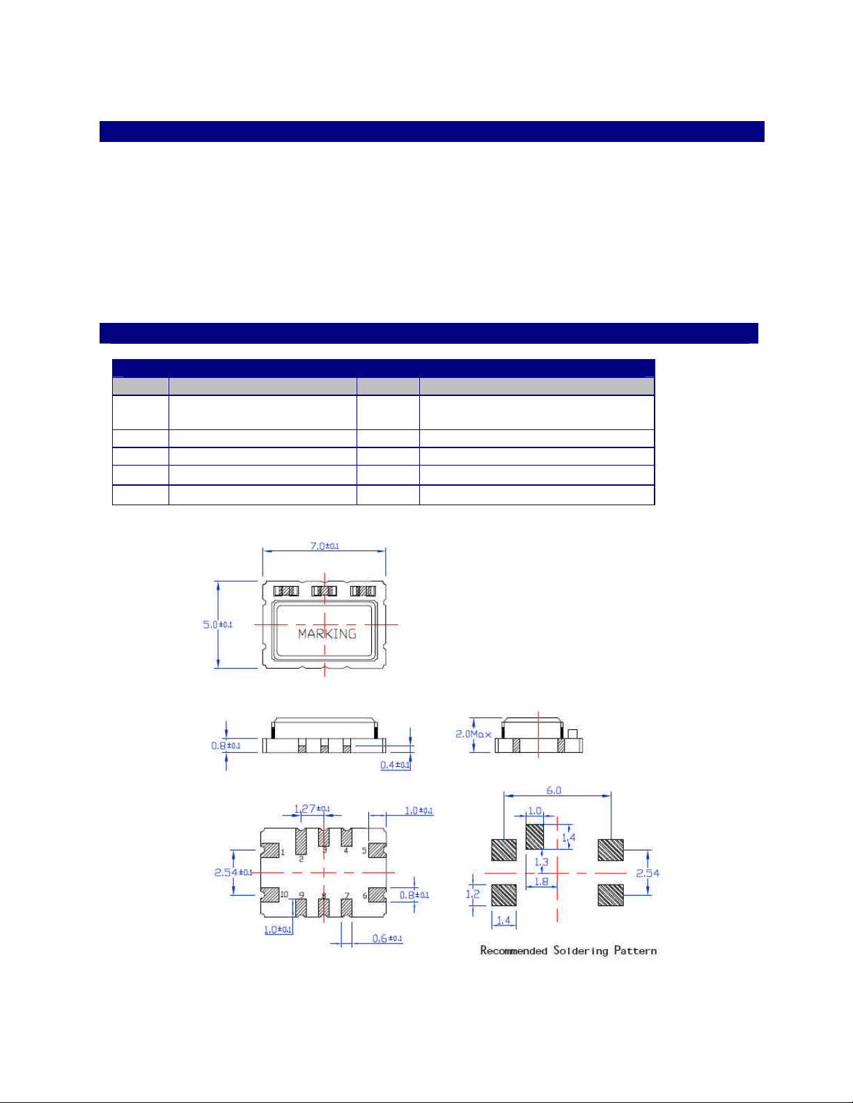
Outline Diagrams, Pad Layout and Pin Out
Table 2. Pinout
Pin # Function Pin # Function
1 No Connect (VTC2-x0xx)
or VCXO Control Voltage
2 Make No Connection 9 Enable/Disable
3 Make No Connection 8 Make No Connection
4 Make No Connection 7 Make No Connection
5 Electrical Ground 6 Output Frequency
NOTE: Additional pads are used to program and adjust the TCXO during manufacturing and should be left
open; do not terminate these to the supply voltage.
10 Supply Voltage
Contact Pads are gold over nickel
Figure 2, Package drawing
Vectron International 267 Lowell Rd, Hudson NH 03051 Tel: 1-88-VECTRON-1 e-mail: vectron@vectron.com

VTC2 Data sheet
Tape and Reel
Table 3. Tape and Reel Dimensions (mm)
Tape Dimensions Reel Dimensions # Per
Product A B C D E F G H I J K L Reel
VTC2
16 7.5 1.5 4 8 1.5 20.2 13 60 2 16.4 180
J
F
CD
A
E
G
B
I
L
KH
1000
Absolute Maximum Ratings
Stresses in excess of the absolute maximum ratings can permanently damage the device. Functional
operation is not implied at these or any other conditions in excess of conditions represented in the
operational sections of this data sheet. Exposure to absolute maximum ratings for extended periods may
adversely affect device reliability.
Table 4. Absolute Maximum Ratings
Parameter Symbol Ratings Unit
Storage Temperature Tstorage -55/125 °C
Reliability
The VTC2 qualification tests have included:
Table 5. Environnemental Compliance
Parameter Conditions
Mechanical Shock MIL-STD-883 Method 2002
Mechanical Vibration MIL-STD-883 Method 2007
Temperature Cycle MIL-STD-883 Method 1010
Solderability MIL-STD-883 Method 2003
Gross and Fine Leak MIL-STD-883 Method 1014
Resistance to Solve nts MIL-STD-883 Method 2015
Moisture Sensitivity Level 1
Contact Pads Gold over Nickel
Vectron International 267 Lowell Rd, Hudson NH 03051 Tel: 1-88-VECTRON-1 e-mail: vectron@vectron.com

VTC2 Data Sheet
Handling Precautions
Although ESD protection circuitry has been designed into the the VTC2, proper precautions should be taken
when handling and mounting. VI employs a Human Body Model and a Charged-Device Model (CDM) for
ESD susceptibility testing and design protection evaluation. ESD thresholds are dependent on the circuit
parameters used to define the model. Although no industry wide standard has been adopted for the CDM, a
standard HBM of resistance = 1.5kohms and capacitance = 100pF is widely used and therefore can be
used for comparison purposes.
Table 6. ESD Ratings
Model Minimum Conditions
Human Body Model 1500 MIL-STD-883 Method 3115
Charged Device Model 1000 JESD 22-C101
Suggested IR profile
Devices are built using lead free epoxy and can also be subjected to standard lead free IR reflow conditions,
Table 7 shows max temperatures and lower temperatures can also be used e.g. peak temperature of 220C.
Table 7. Reflow Profile (IPC/JEDEC J-STD-020B)
Parameter Symbol Value
PreHeat Time
Ramp Up
t S 150 sec Min, 200 sec Max
R
3 oC/sec Max
UP
Time Above 217 oC t L 60 sec Min, 150 sec Max
Time To Peak Temperature
Time At 260 oC (max)
Time At 240 °C (max)
Ramp Down
t
480 sec Max
AMB -P
t P 10 sec Max
tp2 60 sec Max
R
6 oC/sec Max
DN
Vectron International 267 Lowell Rd, Hudson NH 03051 Tel: 1-88-VECTRON-1 e-mail vectron@vectron.com
5

VTC2 Data Sheet
Ordering Information
Table 8. Standard Frequency List
10.000 12.800 16.000 18.000 19.200 20.000 24.000 25.000
26.000 27.000
VTC2 - -
Product Family Output Frequency
TCXO, 5x7 In MHz
Voltage Options Temperature Options
H: +5.0 Vdc ±5%, CMOS Output A: 0 to 55°C
J: +3.3 Vdc ±10%, CMOS Output B: -10 to 60°C
C: -20 to 70°C
Pulling Range D: -30 to 80°C
0: Fixed TCXO, no adjust E: -40 to 85°C
1: ±5ppm
2: ±8ppm Stability Options
A: ±0.5ppm
1: ±1.0ppm
B: ±1.5ppm
2: ±2.0ppm
C: ±2.5ppm
J
0 C
2
10M000
3: ±3.0 ppm
Note: Not all combinations are available: D: ±3.5ppm
±0.5 ppm is available over 0 to 55 °C only 4: ±4.0ppm
±1.0 ppm to ±5.0 ppm is available on all temperature ranges 5: ±5.0ppm
USA: Vectron International • 267 Lowell Road, Hudson, NH 03051
• Tel: 1-88-VECTRON-1 • Fax: 1-888-FAX-VECTRON
EUROPE: Landstrasse, D-74924, Neckarbischofsheim, Germany •
Tel: 49 (0) 7268 8010 • Fax: 49 (0) 7268 801281
www.vectron.com
Vectron International 267 Lowell Rd, Hudson NH 03051 Tel: 1-88-VECTRON-1 e-mail vectron@vectron.com
ASIA: Vectron Asia Pacific Sales 1F~2F. No.8 Workshop No.308 Fenju Rd.,
WaiGaoQiao Free Trade Zone, Pudong New Area Shanghai, China 200131
•Tel: 8621 50480777 • Fax: 8621 50481881
6
For Additional Information, Please Contact:
March 26, 2007
 Loading...